Electrical measurements - UiO
62
1 KJM-MENA 4010 Electrical measurements Emphasising simple methods and instruments, materials aspects, electrochemistry, and impedance spectroscopy Truls Norby Department of Chemistry, University of Oslo FERMIO Gaustadalléen 21 NO-0349 Oslo, Norway
Transcript of Electrical measurements - UiO

1
KJM-MENA 4010
Electrical measurements
Emphasising simple methods and instruments, materials aspects, electrochemistry, and
impedance spectroscopy
Truls Norby
Department of Chemistry, University of Oslo
FERMIO
Gaustadalléen 21
NO-0349 Oslo, Norway

2
Welcome to KJM-MENA4010, Module 2; Electrical measurements
In this module we will learn the most important principles of making electrical
measurements in general, i.e., to obtain voltages and currents using the appropriate
instruments and connections, and to understand and minimize sources of error.
Furthermore, we will discuss selected electrical measurement methods used to obtain
chemical and physical information of liquids, solids, and interfaces. In addition to DC
methods we will focus on AC measurements and impedance spectroscopy.
As practical skills we aim at the end of the course to
- Be able to perform simple electrical measurements of voltage, current, and
resistance, as well as more sophisticated, scientific electrical measurements,
- master handheld and more accurate stationary multimeters and understand their
differences,
- have some knowledge of use of AC signals, AC generators, and an oscilloscope,
- have some knowledge of use of a potentiostat/galvanostat,
- have some knowledge of use of impedance spectrometers.
The course is considered passed when the student has fulfilled all of the following:
- attended a major part of the lectures,
- done all exercises, filled in the result forms, and had them accepted by the
lecturer,
- calculated the electrical response of a hypothetical sample or a circuit as provided
by the lecturer, and presented the result in a short (2-3 page) report,
or
deconvoluted an impedance spectrum measured by the student or provided by the
lecturer using EQUIVCRT software.
Supervision will be available during the exercises, calculations and deconvolutions.

3
Contents
Electrical measurements ..................................................................................................... 1
Welcome to KJM-MENA4010, Module 2; Electrical measurements ............................ 2
Contents .......................................................................................................................... 3
Some definitions relating to voltage and current ............................................................ 5
Voltage and current..................................................................................................... 5
Mobility, conductance, resistance, Ohm’s law ........................................................... 5
Direct and alternating current (DC and AC)............................................................... 7
Electrical circuit elements and circuits ........................................................................... 8
Passive electrical circuit elements............................................................................... 8
Parallel and series connections ................................................................................. 10
Active and non-linear electrical circuit elements...................................................... 11
Symbols for circuit elements..................................................................................... 13
Measurements of voltage, current and impedance........................................................ 13
Voltage...................................................................................................................... 14
Current ...................................................................................................................... 15
Impedance – basic principles and methods............................................................... 15
AC impedance........................................................................................................... 17
Error and accuracy ........................................................................................................ 20
Thermal and other offsets ......................................................................................... 20
Noise ......................................................................................................................... 21
Accuracy ................................................................................................................... 21
Parasitic impedances and admittances ...................................................................... 22
Correction for sample geometry in impedance measurements ................................. 23
Grounding, guarding, screening.................................................................................... 25
Floating and grounded measurements....................................................................... 25
Guarding ................................................................................................................... 26
Shielding ................................................................................................................... 27
DC voltammetry and related techniques ....................................................................... 29
Electrochemical processes at electrode-electrolyte interfaces .................................. 29
Semiconductor junctions........................................................................................... 33
Impedance spectroscopy ............................................................................................... 34
General ...................................................................................................................... 34
Generation and representation of example model spectra ........................................ 34
Physical systems and equivalent circuits .................................................................. 36
Deconvolution and fitting of measured spectra ........................................................ 42
Further considerations of data from impedance spectroscopy.................................. 43
Some specialties of advanced impedance spectrometers .......................................... 44
Combining impedance spectrometers with other units; electrochemical interfaces,
boosters, dielectric interfaces.................................................................................... 45
Some related techniques ........................................................................................... 46
Selected special techniques........................................................................................... 46
Seebeck coefficients.................................................................................................. 46

4
Concentration cells and transport number measurements......................................... 46
Measurements of conductivity etc. on thin films...................................................... 46
Coulometric titration................................................................................................. 46
High frequency measurements and use of transmission lines................................... 46
Exercises ........................................................................................................................... 47
Equipment ..................................................................................................................... 47
Exercise 1: Simple instruments, measurements, and terms ............................................ 1
Identify and check fuses.............................................................................................. 1
Measure DC voltage.................................................................................................... 1
Measure DC current .................................................................................................... 1
Measure resistance ...................................................................................................... 2
Exercise 2: Capacitors..................................................................................................... 2
Exercise 3: Diodes and transistors .................................................................................. 3
Exercise 4: Input and output resistance........................................................................... 4
Exercise 5: AC voltage and current ................................................................................ 4
Exercise 6: Impedance measurements; 2 and 4 wires, 2 and 4 electrodes ...................... 5
Exercise 7: AC impedance measurements ...................................................................... 6
Series circuit; AC impedance...................................................................................... 6
Parallel circuit; AC admittance................................................................................... 6
Parallel circuit represented as impedance ................................................................... 7
Exercise 8: Error sources ................................................................................................ 7
Contact potentials and contact resistance.................................................................... 7
Thermal offsets ........................................................................................................... 8
Static charging and noise ............................................................................................ 8
Parasitics ..................................................................................................................... 9
Exercise 9: Grounding, guarding, shielding.................................................................. 10
Grounding ................................................................................................................. 10
Guarding ................................................................................................................... 11
Shielding ................................................................................................................... 11
(Optional) Exercise 10: Voltammetry........................................................................... 12
Voltammetry (chronovoltammetry) .......................................................................... 12
Exercise 11: Impedance spectroscopy........................................................................... 13
Generate a spectrum.................................................................................................. 13
Deconvolute the spectrum......................................................................................... 13
Deconvolute a given spectrum.................................................................................. 14
Calculate the electrical response of a given sample.................................................. 14

5
Some definitions relating to voltage and current
Voltage and current
Voltage, U, is the difference in electrical potential, φφφφ, between two locations: U = ∆φ =
φ2 - φ1. The unit for voltage U is V (volt).
Electrical field, E, is the negative of the gradient in electrical potential, i.e. it is
defined to be directed from positive to negative pole: E = -dφ/dx. If the gradient is linear
and homogeneous, the voltage over a length L is U = -EL.
Current, I, results from the flux of charged particles. The unit for current is A
(ampere). 1 A = 1 C/s (coulomb per second). There are 96485 C/mol of elemental charges
(e.g. electrons). Consequently 1 A corresponds to ca 10-5
mol/s (of charges).
1 A over a voltage of 1 V gives a power P = UI = 1 W (watt). 1 W for 1 s gives 1
J (joule) of energy.
Figure 1. Schematic illustration of potential, voltage, field, current, and power in relation to current
passing through a resistor.
Mobility, conductance, resistance, Ohm’s law
In the following we derive some simple relationships between voltage and current valid
for constant voltage and current in homogeneous media (conductors).
If a particle has charge ze, it feels a force F = zeE in the electrical field E. This
gives rise to a velocity v = BzeE, where B is the mechanical mobility of the particle. If we
define a charge mobility u = Bze, then v = uE. The flux density of particles then
becomes j = cv = cuE, where c is the volume concentration of particles. The current

6
density is obtained by multiplying the flux density by the particles’ charge: i = zej =
zecuE. Current is then obtained by multiplying by the cross-sectional area A: I = iA. By
replacing E with U/L we finally get I = zecuUA/L.
The product of concentration x charge mobility x charge is called conductivity σσσσ:
σ = zecu (1.)
and when multiplied with area and divided by length we get conductance G:
G = σA/L (2.)
Conductance, G is a property that relates to a particular sample, and has unit S (siemens)
while conductivity σ (often called specific conductivity) is a materials property with unit
S/m. Because samples typically are of sizes in the cm-range, tradition has made it
common to use S/cm rather than the SI unit S/m.
The inverse of conductance is resistance R = 1/G and the inverse of conductivity
is resistivity ρρρρ = 1/σ. Obviously, R = ρL/A. The unit for resistance is ohm (=1/S).
We can now from the above equations and definitions express the current as
I = UG = U/R (3.)
known as Ohm’s law.
We have not said anything about the physical basis for mobility of charge carriers.
It can be derived from various formalisms, e.g. diffusion or collisions, depending on the
type of transport and the traditions in different fields of application and science.
Moreover, we have not said anything about the concentration of charge carriers, which
depends on materials, temperature and composition. While these are the interesting
parameters for us as chemists, physicists or materials scientists, this course is not so much
about that. Instead it is about the methodology to measure electrical properties as part of
what may be needed to get hold of those parameters.
Figure 2. Schematic illustration of terms relating to current and resistance

7
Direct and alternating current (DC and AC)
The voltage and resulting current can be constant with time and are then referred to as DC
(from “direct current”).
The voltage can also be varied in numerous ways, e.g. referred to as sine, square
or sawtooth waves, noise, etc. Most important, and the only we will treat here, is the sine
voltage, resulting in sine current and thus referred to as AC (from “alternating current”).
The sine voltage is characterized by its frequency f and angular frequency ωωωω = 2πf as
well as its amplitude U0:
tUU ωsin0= (4.)
The amplitude can also be specified as the peak-to-peak voltage, Up-p = 2U0 or the root
mean square (rms) voltage Urms = U0/√2 = Up-p/(2√2).
The term tω is called the phase angle. A sinusoidal AC current resulting from the
applied AC voltage will have the same frequency as the voltage, but may have different
amplitudes and phase angles:
)sin(0 θω += tII (5.)
The phase shift θ results from capacitive (non-ohmic) elements in the circuit.
A sine AC voltage or current can be superimposed on a DC voltage Ub or current
Ib. The DC part of the voltage or current is called bias, and shifts the AC curve off
symmetry around zero voltage or current.
Figure 3. Left: AC voltage and current. Right: Biased AC voltage.
Sine waves can be troubled by harmonics (usually overharmonics; presence of
voltage and current components that is a multiple of the fundamental frequency) or
distorsion (deviations from ideal sinusoidal curve form). These are usually generated by
the AC source itself or by non-ideal electronic components in the electric pathway.
We will treat AC signals in more detail later, under impedance spectroscopy.

8
Electrical circuit elements and circuits
Passive electrical circuit elements
We now consider some passive electrical circuit elements, in the form of discrete
components. This is partly because we need to understand electrical circuits and drawings
of them, partly because we need to know and to use some of them in our exercises
onwards, and partly because we need to know their behaviour as a function of frequency.
Resistors (conductors)
A resistor (or conductor) is an element with long-range transport of charge carriers. The
number of charges, concentration, and mobility of the charge carriers give rise to
conductance G and resistance R = 1/G as we have discussed earlier. In an ideal resistor,
voltage gives rise instantly to current and vice versa. Thus, AC voltage and current in a
resistor are in phase. Power (heat) is dissipated in the resistor, and via integration of
P=UI over one period it turns out to be:
2sin
11 00
0
2
00
0
UItdtUI
TUIdt
TP
TT
=== ∫∫ ω (6.)
The resistance is given as
0
0
0
0
sin
sin
I
U
tI
tU
I
UR ===
ωω
(7.)
i.e. identical to the DC case. Note that the resistance of a resistor is independent of the
frequency.
Resistors for electronic circuitry come in many fashions. Computers would
nowadays have many of the resistors built into chips or integrated circuits. When using
single (discrete) resistors, we need to deal with the nominal value and perhaps accuracy,
power rating, and temperature coefficient. A colour coding scheme is in use for small
discrete resistors with small power ratings (typically ¼ W). For low-accuracy resistors
this is given as 2 rings for value and one ring for the number of additional zeros. The
colours are black=0, brown=1, red=2, orange=3, yellow=4, green=5, blue=6, violet=7,
gray=8, white=9. For instance, brown-black-red means 10 + 2 zeros = 1000 ohm = 1
kohm and brown-green-blue means 15 000 000 = 15 Mohm. In addition, a fourth ring
may signify the accuracy: Silver=10%, Gold=5%.
Exercise at this stage: 1. Simple instruments, measurements, and terms

9
Capacitors
A capacitor comprises an ideal insulator between two conductors. Most typically it is
constructed as parallel plate conductors separated by vacuum, a gas, or dielectric material.
The plates can be charged by applying a voltage over them; a current flows in the leads to
the plates, and the charges end up in the plates where they are attracted to the opposite
charges in the other plate. The larger the area and the shorter the distance between the
plates, the smaller is the voltage needed to store a certain charge. The capacitance is
defined as C = Q/U and has unit F (farad). The charge Q has unit C (coulomb). Thus, a
capacitor has capacitance 1 F if 1 C of charge gives 1 V over the plates.
If a polarizable medium is placed between the plates, the dipoles of that medium
becomes directed according to the electrical field set up by the voltage. The orienting of
the dipoles depolarizes the field between the plates and reduces the voltage over them.
Thus, the capacitance increases. The ratio between the new capacitance and the
capacitance without a medium (vacuum) is called the relative permittivity εr of the
medium, and in general the capacitance of a capacitor is given as
d
AC rεε0= (8.)
where εr is the permittivity of vacuum, A is the area and d the distance between the plates.
Figure 4. Depolarisation of a capacitor by dipoles in the dielectricum.
Since the current to a capacitor is the change in its charge Q with time, we have I
= dQ/dt = C dU/dt. With an applied AC voltage as above, we further get
)2
sin(cos)sin(
00
0 πωωωω
ω+=== tCUtCU
dt
tUdCI (9.)
The current over a capacitor is thus phase-shifted π/2 (or 90°) ahead of the AC voltage
over it.
The power dissipated over the capacitor is zero:
0cossin1
0
2
0
0
=== ∫∫TT
tdttT
CUUIdt
TP ωω
ω (10.)

10
The ratio between the peak voltage and peak current when an AC voltage is
applied over a capacitor is RC = 1/(ωC) and is called the capacitive resistance. We shall
see later that it is not a real resistance. However, we may note that it is inversely
proportional to the frequency.
Discrete capacitors come in various types. Small capacitances are obtained using
e.g. ceramic dielectrics. Larger ones are accomplished by so-called electrolytic capacitors
having very thin electrochemical double-layers between an electrolyte and the electrode.
An important parameter for capacitors is the maximum voltage rating before breakdown.
For electrolytic capacitors this is usually modest, and is furthermore directional, i.e. the
capacitor only tolerates voltage in one direction, not backwards.
Inductors
The last linear (passive) circuit element we shall mention here is the inductor. This is
ideally simply a length (straight or coiled) of an ideal conductor with no resistance. If a
sinusoidal current passes in the conductor, a corresponding magnetic field is set up
around it, and this in turn induces an AC voltage UL over the conductor. The AC voltage
U that was applied originally to pass the current must have been equal and oppositely
directed as UL:
)2
sin(cos)sin(
00
0 πωωωω
ω+====−= tLItLI
dt
tIdL
dt
dILUU L (11.)
where L is the inductance of the inductor. The unit for inductance is henry, H. Thus, here
the voltage is π/2 (or 90°) ahead of the current. Also here, the dissipated power is zero.
The inductive resistance is RL = ωL (i.e. proportional to frequency).
There is in principle no difference between a coil and a normal conductor with
respect to it acting as an inductor, the coil is just a more efficient way of packing a long
length of conductor. The inductance is proportional to the susceptance of the medium that
the magnetic field is set up in, and placing a material with high susceptance as the core in
a coil gives the coil a high inductance.
Parallel and series connections
Electrical circuits consist of connections of various elements, in series and/or in parallel.
In order to deal properly with circuits we need to know the laws of summation of currents
and voltages.
Kirchhoff’s 1st law says that the sum of currents flowing into a branching point is
equal to the sum of currents flowing out in the branches. In other words, the total current
equals the sum of currents in all parallel pathways; current is summed in parallel. Since
Exercise at this stage: 2. Capacitors
11
the voltage over each parallel branch is the same, the current flowing in each is
proportional to the conductance (or inversely proportional to the resistance) of that
branch.
Kirchhoffs 2nd
law says that the sum of all potential changes (voltages) in a chosen
direction around a closed circuit is zero. In other words, voltages are summed in series.
Since the current is the same in all serial parts of the circuit, the voltage over each part is
proportional to the resistance of that part.
Active and non-linear electrical circuit elements
Among many other types of elements representing discrete components as well as
physical or chemical processes in materials and interfaces, we shall only mention
rectifying junctions, such as in diodes and transistors made from semiconductors. This is
because some knowledge of them enables understanding of how electrical instruments
affect the measured signals. They are also representative of non-linear components.
Diodes
A diode is a connection between a p-type and an n-type semiconductor; a p-n junction.
On the interface between the two we have a depletion zone, where neither holes or
electrons are present for conduction.
When current flows in a direction where electrons move away from the depletion
zone (and holes similarly move away in the opposite direction), the junction becomes
insulating; this is the blocking direction of a diode. If, on the other hand, the current is
reversed, electrons and holes flow into the depletion zone, making the junction
conducting. The diode now conducts. In effect, the diode is a rectifier.
Figure 5. Illustration of a pn junction and its conducting and blocking actions under forward and reverse
bias.
Transistors
A transistor contains an assembly of three layers of semiconductors: n-p-n or p-n-p. The
first junction in each is put under forward bias, while the next is blocked (reverse bias).

12
However, charge (voltage) is supplied to the central layer (base) to counteract the
depletion of the second junction and causing current to flow. The current is proportional
to the input voltage on the base, and a small DC or AC or otherwise modulated signal can
thus be amplified to a large current.
Figure 6. Illustration of a pnp transistor and its use as an amplifier.
Transistor-based amplifiers are used both to generate electrical voltages and
currents, and to measure voltages. In generators, the impedance of the transistor should be
low, so that the circuit connected does not change significantly the output voltage.
Correspondingly, the input stage of an amplifier used for voltage measurements should
have a high resistance so that it does not draw significant currents from the circuit being
probed. As a general rule in voltage measurements, an output stage should have much
smaller resistance than the following input stage.
Figure 7. Schematical illustration of the internal resistance Ri of a DC voltage source (generally any
generator, transistor, battery, fuel cell, etc.) and the input load resistance Rl of an input stage (e.g.
voltmeter, amplifier).
The introduction of so-called Metal Oxide Field Effect Transistors (MOSFETs)
enabled input stages that draw only minute amounts of charge, i.e. with very high input

13
resistances. This has, in turn, enabled faster and less power-consuming digital computer
circuits, but also voltmeters that can probe voltages generated over large internal
resistances.
Figure 8. In this MOSFET transistor, the p.type channel is normally depleted and thus blocking because of
its neighbouring n-type substrate. However, input signals to the gate charges the channel electrostatically
through the thin insulating oxide layer. This opens the otherwise depleted channel and allows current to
pass between source and drain.
Symbols for circuit elements
The figure below shows some common elements and typical symbols used for them in
circuit diagrams.
Figure 9. Symbols for resistor (R), capacitor (C), inductor (L), DC voltage source (U), diode (D),
transistors (T).
Measurements of voltage, current and impedance
We will now deal with the actual measurements of voltage and current, and, in turn,
impedance. We will only partially touch the actual physics of the measuring equipment,
as this is highly sophisticated and complex electronics in most cases. All three parameters
may be direct or indirect measures of the thermodynamics of a chemical reaction, the
Exercise at this stage: 3. Diodes and transistors
14
difference in potential of electrons, the number and flux of charged chemical or physical
species, the mobility of the same, etc. Here we will however generalize, and deal with the
measurements as such.
Voltage
Originally, voltage - DC voltage that is - was measured by electrometers; here the
voltage to be measured was contacted to two objects in vacuum, e.g. a fixed one and a
foil. The deflection of the foil indicated the charge and thus the voltage on the objects.
Since no current could float through the vacuum, the device had infinitely high resistance.
Therefore, high input resistance voltmeters are today also sometimes referred to as
electrometers.
In more modern times it became more practical to use voltmeters where the
voltage created a tiny current through the coil of an electromagnet on an indicator and
caused the indicator to move on a panel against a very soft spring force. This is used in
many simple handheld analog multimeters and panel instruments. The input impedance of
such instruments is usually modest, e.g. 10 kohm, and the accuracy also poor. They are
thus only useful for simpler test and service applications. Multimeters and other simple
analog instruments can measure AC voltages by rectifying them over one or more diodes
before measuring the resulting DC voltage as above. This makes the AC measurement
less sensitive, and correct only over a rather restricted frequency range. The various
voltage ranges of analog instruments come about by attenuating the voltage over
selectable voltage dividers (with selectable ratios of resistors).
Modern hand-held (battery-powered) multimeters use electronic circuitry to
measure voltage, and display the result digitally. The input amplifiers may have
reasonably high resistances, e.g. 1 Mohm. They thus measure various voltage sources
with better reliability than analog ones, and with better accuracy and resolution, typically
four digits or 0.01 %.
Instrumentation (stationary) multimeters are not necessarily much different than
hand-held digital ones, but being associated with higher cost and power consumption they
usually have more features, larger measurement ranges, and computer communication.
More importantly for us, they have higher input resistances, typically 109 – 10
12 ohm (1-
1000 Gohm) or even higher in the case of electronic electrometers. Moreover, they can
typically reach a resolution of 6 digits or 1 ppm. They may have features like filtering or
averaging that take some noise or variations out of DC measurements. Another useful
feature is the auto-ranging that lets you automatically get the highest available resolution.
We finally mention the oscilloscope. This device measures a voltage and displays
it graphically versus time or versus another voltage. The time base can be selected freely
or one may use the AC component of the voltage to trigger the time base and thus display
the voltage as a standing wave. The oscilloscope is useful for displaying combined DC
and AC signals as well as the actual wave-forms, i.e. noise, over-harmonics, distortion,
phase-relationships etc.
Exercise at this stage: 4 Input and output resistance

15
Current
For all practical purposes we can assume that current is measured by passing the current
over a standard resistor and measuring the voltage generated in the same manner and by
the same instruments as listed under voltage measurements. Thus, current can be
measured by simple analog instruments and multimeters, and by stationary multimeters
and electrometers. Both AC and DC currents can be measured. The quality of the
measurement follows that of the voltage measurement and of the standard resistors. The
current ranges are set by selecting resistor and/or voltage divider, but these processes are
usually hidden to the user.
In the voltage measurements we have discussed above, the input resistance should
be as high as possible. In current measurements the resistance (the standard resistor)
should be as small as possible in order to affect the current as little as possible.
Impedance – basic principles and methods
Impedance is a more general expression for what we have called resistance up to now.
While resistance mainly is used for DC conditions, impedance covers both AC and DC. It
is the ratio of voltage over current. It has units of ohm. Measuring it is thus a matter of
measuring voltage and current – it’s as simple as that.
That is, it is that simple today, since we benefit from automated and intelligent
devices that measure both voltage and current with ease and accuracy, as described above.
Earlier impedance measurements were done by Wheatstone’s bridges; devices where
current was run in two parallel paths, and components on one side changed manually until
they accurately matched that of the sample, as monitored by measuring the voltage
developed between the two paths. We will not deal any further with such devices here.
Nowadays we measure the impedance of a test object by
1) Generating a voltage (AC or DC) that is applied to the circuit of which the
object is part, thereby getting a current through the circuit,
2) measuring the voltage UD developed over the device under test, and
3) measuring the current I in the device by measuring the voltage Us generated
over a standard resistor Rs placed in the circuit.
We divide the numbers and obtain the impedance; ZD = UD/I = UD/(Us/Rs). If we
wish, we may multiply by the cross-sectional area A of the object or test cell in order to
get area-specific impedance, and further divide with the length l (distance between
electrodes) if we want to get the (volume-)specific impedance.
The accuracy of the overall measurement is best if the standard resistor has a
value of the same order of magnitude as the sample. In the following, we will not discuss
in any further detail the selection of standard resistors - we assume this is something you
do manually, or the impedance measuring device does automatically.
Exercise at this stage: 5 AC voltage and current

16
Handheld instruments use battery power to supply a DC signal, while stationary
instruments may supply higher quality DC or AC signals. It may be noted that the current
or voltage output from the instrument to the sample need not be constant or at a particular
value, as long as the actual current is measured. For instance, the sample may well have a
lower resistance than the output stage of the instrument, so that the actual voltage output
is lower than nominal – without causing a problem. Many instruments have feedback
circuitry that ensures that the output voltage or the voltage developed over the sample
stays at a predefined value (potentiostatic mode) or that the current stays at a predefined
value (galvanostatic mode).
Impedance devices may have a number of terminals, varying between 2 and
something like 6. However, the standard is to have 4 terminals: Two for the current loop
(including generator and internal current measurement) and two for the measurement of
voltage over the object. If it has only two, then the voltage is measured over the object at
the terminals of the current loop. If it has 6 terminals, then the two last ones may be used
for measuring the current over an external standard resistor placed in the current loop.
In addition to these terminals, instruments may also have a range of shield and
ground terminals; we shall come back to their functions later.
The main concern in impedance measurements is to ensure that the voltage you
measure is the one developing over the part of the object that you are interested in, and
that the current you measure is the current running in the part of the object that you are
interested in. The former is usually our biggest concern, and we shall deal with that in
some detail in the following.
There are numerous impedances in series with the object under test. They all
develop voltage by the current in the loop. Where we measure the voltage – i.e., where we
attach the voltage probes in the current loop - will determine which contributions we get
included in our impedance result.
2-wire 2-electrode measurements: If the instrument has only 2 terminals or if the
current and voltage terminals are connected close to the instrument, the measurement
effectively includes the impedances of the wires (and any bad contacts on the way), the
electrodes and the sample. This mode is only acceptable in simple test routines or if the
sample or object under test exhibits a large impedance compared with the other
contributions. Simple hand-held multimeters operate in this mode, and cannot measure
accurately resistances (impedances) below, say, 1 ohm.
Figure 10. Schematical principle of resistance measurements using 2 electrodes and 2 wires. Left: 2-
terminal instrument (typical handheld).Right: 4-terminal instrument. In both cases the wires to the device
(D) contribute to the voltage drop and thus to the resistance. The terminology IH, UH, UL, IL for the four
terminals is typical, reflecting current and voltage terminals in order of going from high to low potential.
17
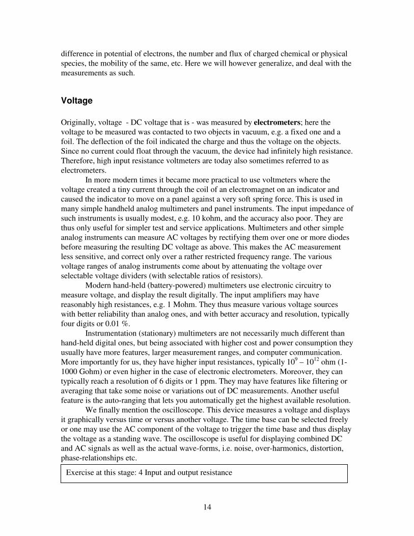
4-wire 2-electrode measurements: By letting the voltage probe wires run
separately all the way to the object under test, we eliminate the resistance in the current
wires, and need in principle not worry about poor contacts or too thin, resistive wires. The
measurement then includes only the electrodes (contacts) and the sample.
4-electrode (often called 4-point) measurements: By letting the voltage wires
probe the voltage using separate electrodes on the sample, also the impedance of the
current electrodes are eliminated. The measurement then includes only the sample
substance.
Figure 11. 4-terminal instruments used with 4 wires. Left: 2-electrode measurement (sample and
electrodes). Right: 4-electrode measurement (sample material only).
3-electrode measurements: This mode is a combination of the 2- and 4-electrode
modes, and is used to study electrode impedances. One electrode is used as both current
and voltage probes, and the impedance of this electrode is thus included in the
measurement. This electrode is called the Working electrode. The two other are the
Counter electrode for current and the Reference electrode for voltage. Since the reference
electrode is free of current, its impedance is excluded from the measurement. 3-electrode
measurements may use 3 or 4 wires, i.e., the working electrode may be contacted by one
or two wires.
AC impedance
.
As we have seen previously, AC voltage and current may be out of phase with each other.
Thus, the ratio between the two has a phase angle.
In AC impedance measurements, current and voltage are measured as sinusoidal
voltages, one over the sample and one over a reference resistor. In addition to the
magnitude of the two voltages, the device measures the phase angle between the two.
Alternatively, the current may be taken to have two components; one that is in
phase with the voltage, and one that is 90° degrees out of phase, and the impedance-
measuring device may work by splitting the current into those two components. The
Exercise at this stage: 6 Impedance measurements; 2 and 4 wires, 2 and 4 electrodes

18
result is thus given as one impedance which is the voltage divided by in-phase component
of current, and one which is the voltage divided by the 90° out of phase component of
current.
The in-phase part of the impedance is called the real part. This reflects that it
comprises real, impeded transport of charge carriers through the impedance element and
that it gives rise to heat dissipation when AC current passes. The real part of an
impedance is called resistance, R. A resistor is an example of a component with real
impedance.
The 90° out of phase component of impedance is called the imaginary part. This
may reflect that charge carriers are not really transported through the impedance (only
stored there temporarily, as in an ideal capacitor) or are not really impeded (as in an ideal
coil). Imaginary parts of impedance do not give rise to heat dissipation when AC current
flows through it. The imaginary part of the impedance is denoted reactance, X.
Figure 12. Representation of complex impedance (left) and complex admittance (right) in Cartesian
coordinates.
The total impedance may now be taken as a vector in the two-dimensional real-
imaginary space. The impedance Z is then represented as a complex number – the
complex impedance Z*:
Z* = Z
/ + jZ
// = R + jX (12.)
We recall from the introduction of resistors, capacitors and inductors (coils) that they
have resistances given by R, RC=1/(ωC), and RL=ωL. The first is real, while the two latter
are imaginary. Moreover, the actual division of voltage by current in an ideal capacitor
comes out as -RC = -(1/ωC) such that the impedance of a series connection of a resistor, a
capacitor, and a coil is
LjC
jRL
CjRZ ω
ωω
ω+−=+
−+= )
1(* (13.)
The inverse of impedance is admittance: Y* = 1/Z
*. It is obtained as the ratio
between current and voltage, and is similarly to admittance a complex number. The real
part of admittance is called conductance, G, and the imaginary part is called
susceptance, B:

19
Y* = Y
/ + jY
// = G + jB (14.)
An ideal resistor is also an ideal conductor and for this we have G = 1/R. For an ideal
capacitor we have BC = -1/XC = ωC and for an ideal inductor (coil) we have BL = -1/XL =
-1/(ωL). A parallel connection of a resistor (conductor), a capacitor and a coil thus has
three contributions to admittance – one real and two imaginary:
L
jCjG
LCjGY
ωω
ωω −+=
−++= )
1(* (15.)
Let us briefly look at the conversion from impedance to admittance:
22222222*
*
)())((
11
XR
jX
XR
R
XR
jXR
jXR
jXR
jXRjXR
jXR
jXRZY
+−
+=
+
−=
−
−=
−+−
=+
==
(16.)
Similarly,
2222*
* 1
BG
jB
BG
G
YZ
+−
+== (17.)
We see that the transformation leads to a new complex number based on the
components of the other representation. However, the transformation between R in the
series representation to G in the parallel representation is not a straightforward inversion
as one might perhaps have thought. Only when there are no significant contributions from
the imaginary parts (B or X are zero) is G = 1/R.
It may be mentioned that the term immitance, I*, is used to denote impedance and
admittance together.
A device measuring AC impedance or admittance does not and cannot know how
to interpret the result. It only knows the ratio of voltage and current and the phase angle.
This it can calculate into Z* = R + jX or Y
* = G + jB. In order to interpret it further, it
must know whether the real part of the impedance or admittance is connected in series or
parallel with the imaginary parts. Many instruments have the possibility to choose
automatically one or the other. For this it uses the total impedance; if it is high it assumes
a parallel connection (between something you probably are interested in and something
else adding up in parallel). If it is low it assumes a series connection. The reasoning
behind this will become clearer in later sections.
If a series connection is chosen (by the instrument automatically or by you
manually) the instrument uses Z* to obtain R and X and in turn calculate the capacitance C
or inductance L of the element that is in series with the real part R. Again, there is in
principle no possibility to separate C and L, so you have to tell which one you want. The
sign of X does however change, depending on which one you have or which one

20
dominates, so that you or the impedance measuring device can make a judgment based on
this. Circuit elements interpreted from an AC impedance measurement based on a series
connection model are denoted Rs, Cs, and Ls.
Similarly, if you tell the device that you have a parallel connection, it uses Y* to
obtain G and B and interprets them in terms of Gp, Cp and Lp. The real part Gp can also be
expressed as parallel resistance Rp = 1/Gp.
We have here described how an AC impedance measurement can be interpreted as
a simple series or parallel connection of one real and one imaginary impedance or
admittance element. If this with sufficient accuracy describes the real situation, then we
have a useful result. A good sign of a correct interpretation is that the element values R,
or G and C or L remain constant independent of applied frequency.
If we don’t know how the elements are connected, or if we may assume that the
circuit is more complicated than a simple connection of two elements, we may measure
complex impedance or admittance over a range of frequencies, and in that way rule out
some combinations. This is what we do in impedance spectroscopy, which we shall deal
with in more detail later on.
Error and accuracy
Thermal and other offsets
Voltages may be introduced in a circuit by contact potentials between different materials
and by thermal asymmetries. These may affect measurements of DC voltage, but also of
DC resistance measurements. For instance, if one attempts to check the state of an
operating thermocouple by measuring its resistance with a multimeter, the thermoelectric
voltage imposed by the thermocouple may well overshadow the voltage set up over the
sample by the current from the instrument. Thus, the reading of resistance will be erratic
and moreover change a lot (e.g. from plus to minus) depending on which direction one
measures in.
Thermal variations and offsets can be attempted reduced by using cables and
components with materials that create small thermoelectric forces. In particular, the two
voltage probes of measurements should be kept symmetric in terms of materials and
temperature gradients.
Stable remaining offsets can often be subtracted by adjusting zero-points of
voltmeters, or in the post-measurement treatment of data.
Offsets can also be part of the instabilities in the measuring instrument itself.
Exercise at this stage: 7 AC impedance measurements

21
Noise
Noise – instabilities in the electrical signals and readings - may have several sources.
Electromagnetic fields may induce voltage and currents in the sample and
measuring circuit. The source may be communication signals (radio, TV etc.), fields from
displays, lamps, and neighbouring scientific equipment, and from the electric currents
used to heat or cool the sample. Noise from external sources thus cover a wide frequency
range, from radio-frequency to hum (50 or 60 Hz). Such noise can thus be reduced by
appropriate filtering or screening.
Many measurements, instruments and circuitry have limited high frequency
response, and are thus insensitive to radio frequency noise.
External noise has to pass an impedance to enter the sample or measuring circuit
whereafter it experiences the impedance of the sample and circuitry; it is attenuated by
the voltage divider consisting of the transfer impedance and sample+circuitry impedance.
Therefore, the lower the impedance of the sample and the circuitry, the smaller the
residual external noise that enter the measurement: A sample with low impedance short-
circuits noise.
Noise may also come from the sample itself. This is thermally generated noise –
fluctuations in the concentrations and energy of charge carriers. Such noise is generated
with a statistical distribution in frequency and level and thus in principle covers all
frequencies.
Finally, noise is also part of the measuring instruments, for the same reasons as
above. Thus, as the measured value approaches zero, some level of noise will inevitably
remain, depending on the quality of the instrument.
Accuracy
Electrical instrumentation (voltmeters and amperemeters) are in general quite
accurate, and often, this accuracy is not the limiting factor in electrical measurements, but
rather factors such as stability, dimensions or composition of the system to be
investigated, or other physical measurements that enter the overall investigation, e.g. for
temperature or chemical potentials.
Resolution is a property of the measuring instrument, e.g. to be able to give the
result with 4, 5, or 6 significant digits. This is eventually reduced by noise.
Precision is related to the zero-level (offsets), which we have treated above, and
which is relatively easy to correct for, by applying zero volts, zero current, zero
impedance or zero admittance – all situations that are fairly easy to realize as long as one
does not ask for extremes.
Accuracy has to do with the slope in actual value vs displayed response, often
called amplification in many electrical measurements. This is where it is more difficult to
check the instrument and where we usually trust it. If we don’t then here is where the
most difficult part of calibration comes in. In order to check a voltmeter you need a
calibration voltage source. In order to check an amperemeter you need basically a
standard resistor above which you measure the voltage with your calibrated voltmeter. In

22
order to check impedance measuring equipment you again need standard resistors as a
minimum.
Other parameters may also affect the accuracy; linearity and, not least,
temperature stability. Most measuring equipment specify the limits of error as a function
of temperature or deviations in temperature. Keep this in mind; note the ambient
temperature in your log-book, check that the fan of the equipment works, and that the fan
and instrument interior is not clogged by dust.
Parasitic impedances and admittances
When measuring impedances we have to be aware of things that add to the impedance,
i.e. things that act in series with our device or sample under test, but are not intended to
be part of the result. These are called parasitic impedances. We also have to be aware of
things that are adding to the admittance of the measurement – things that are in parallel
and thus contribute parasitic admittances. The figure below illustrates the action of
parasitic impedances and admittances. One may object that the connection points of the
two with respect to each other is not obvious, but in practice only one makes a significant
contribution at a time, and then the order of connection is not an important issue.
Figure 13. Parasitic impedance Zp in series and admittance Yp in parallel with a device D.
Parasitic impedances comprise the resistance and inductance in the wires that lead
to the sample. The resistance is typically of the order of an ohm or less. They can be
eliminated by 4-wire measurements. Next we have spreading resistance in the electrode,
contact resistance to the material or electrochemical resistance in the case of an ionic
conductor. If these are not part of the measurement of interest, they can be eliminated by
using 3- or 4-electrode measurements. Finally, resistance and inductance remain as two
elements that make up the impedance of the sample or component under test.
Figure 14. Parasitic impedance elements; resistance and inductance.
Parasitic admittances are parallel to the sample and thus comprise all possibilities
that current has to flow between the two sides of the sample. In DC measurements this
includes transport on and in insulators. In particular, adsorbed humidity on surfaces
provides some conduction. In AC measurements, signals may furthermore be transmitted
between wires across the capacitance in air or insulators. These sources of parasitic

23
admittances are usually attempted eliminated by shielding the conductors from each other
(see below). Parasitic admittance furthermore includes transport on the surface of the
solid samples or components themselves. The latter may be eliminated in some cases by
surface guards (see below). At high temperatures even the gas phase around the sample
provides some conduction; this may be eliminated by physical hinders. The interior of a
solid may provide conduction on the surfaces of open pores, a problem that cannot be
eliminated by other means than to use more dense samples.
Figure 15. Parasitic admittance elements; conductance and capacitance.
Be aware that your hands provide a considerable parasitic admittance if you hold
both terminals of a sample. In the exercises you can measure it with a multimeter or
impedance spectrometer.
In summary, parasitic impedances trouble measurements of low impedances, they
usually have resistive or inductive origins, and are combated using measurements with 4
wires and 3- or 4-electrodes. Using sample geometries that increase the sample’s own
impedance decreases the problem. Similarly, parasitic admittances trouble measurements
of low admittances (high impedances), they usually have conductive or capacitive origins
and are combated using physical or electrical shields and guards. Using sample
geometries that increase the sample’s own admittance decreases the problem.
In a normal measurement of a normal impedance at DC or a normal AC frequency
and with normal demands for accuracy you may often disregard parasitics. When you
move in the direction of low or high impedances you may have to start considering
parasitic impedances or parasitic admittances, respectively, but usually not both.
When you have residual parasitics that you cannot remove but have to correct for,
the parasitic has to be known, estimated, or measured. Often, parasitics can be delineated
by impedance spectroscopy (see below) or by varying a dimension of the sample.
Correction for sample geometry in impedance measurements
In impedance measurements it is usually required to recalculate the results from measured
values into materials specific values. For this we need to correct for the sample’s
geometry and sometimes also microstructure. In measurements on liquids the geometry of
the measurement cell remains constant, and can be measured once and for all or
calibrated against a known standard. The corrections are often collected in a cell constant
that translates e.g. a measured conductance or capacitance into a specific conductivity or
Exercise at this stage: 8 Error sources

24
capacity, that can be used to calculate for instance concentrations of ions or the relative
dielectric constant.
For solids, it is more tricky, since each sample in principle is different, and we
shall consider a few factors of importance.
For disks (2-electrode measurements) the relevant length of the measurement is
the thickness. For bars (4-electrode measurements) the relevant length is the distance
between the voltage probes. Both are straightforward to identify, but usually not easy to
measure with a great deal of accuracy.
For bar samples the relevant cross-sectional area is the one for the part of the
sample that lies between the voltage probes, again straightforward to identify, and
possible to measure with reasonable accuracy.
For disk samples the cross-sectional area may or may not be equal to the
superficial area of the electrodes. This is certainly the case if the electrodes are well
conducting (no spreading resistance) and cover all of two identical surfaces on both sides.
If the electrodes do not cover all of the surface, one may as a first approximation
still use the superficial area if the electrodes are placed symmetrically and the disks are
thin compared to the electrode dimensions. If the electrodes are of different areas one may
then also take the average of the areas.
For symmetrically placed electrodes that are considerably smaller than the sample
area, one may take into account the spreading of the current so as to get a larger effective
area. This becomes increasingly important as the ratio between sample thickness and
electrode dimensions increases.
If the electrodes are not well conducting, the outer parts (away from the contact of
the wires) may contribute less, and a complicated situation will arise. Simply seen, the
effective cross-sectional area becomes smaller than the superficial area. A particular
warning may be issued against having the current and voltage wires contacting different
areas of a poorly conducting electrode; if the current goes in part of the sample and the
voltage is measured elsewhere, the impedance results surely becomes erratic. Thus the
seeming similarity with the 4-point contact mode makes no sense in this case, and it is
better to ensure that the two wires are in good contact with each other and with as much
as possible of the electrode.
After such correction for external sample geometry, one may have to consider its
microstructure, notably porosity. In the following we assume that the pores is an ideally
insulating phase distributed in the matrix of the material whose specific conductivity we
want to obtain. Clearly, the pores affect the measured conductivity depending on how
they are distributed. If they were all laying as planes or coloumns parallel to the current,
the conductivity would be decreased simply according to the volume fraction of pores. If
they were planes normal to the current, the measured conductivity would be zero. In real
samples the effect of pores accordingly vary with their volume fraction (porosity) and
distributions on size, shape, connectivity, and directions (texture), and ends up in between
the two extremes mentioned. For a real sample we must thus rely on empirical
relationships established for that particular type of material. Such relationships are in
general not established at present, and we commonly use a very general one, that seems to
give reasonable corrections for fairly low porosities:

25
σmeasured = σ (1-p)2 = σ d
2 (18.)
where p is the pore fraction and d is the relative density. Thus, a material with 10%
porosity (90% density) is estimated to exhibit only 81% of the true conductivity of dense
material. A measured conductivity is thus to be corrected by division of 0.81 to obtain the
estimate of true material conductivity.
Grounding, guarding, screening
Floating and grounded measurements
A hand-held multimeter in a plastic housing clearly has no sense of ground or other
reference potentials around it. When a voltage is output in a resistance measurement or a
voltage is measured in a voltage measurement, neither of the voltages at the two terminals
is defined with respect to any other voltage in the surroundings. We know the difference
in potential between the two terminals, but we do not know the individual potentials, and
we do not put any restrictions on it. The voltage and the instrument float.
Similarly, a sample may have terminals that are insulated from the surroundings
and thus floating.
Advanced electrical instruments like stationary multimeters and impedance
spectrometers have one or several ground levels. These may comprise the neutral terminal
of the mains power supply (varies between countries), the earth terminal of the mains
power supply, the chassis of the instrument, the zero-voltage of the DC power supply and
electronics of the instrument, and a reference level or zero-potential of the measurement
signals. In general, those of these that are present are more or less connected to each
other, passively or actively, so that they are mostly at the same potential. It is thus usually
sufficient to think of all these as “ground”, but certain applications are sensitive to
currents running between the different physical parts relating to these potentials. In
particular one should be aware that if mains power earth contact is made through several
power chords, external factors may cause currents to flow in our ground system – we
have unwanted earth-loops. Similarly, physical contacts to the laboratory building etc.
may provide loops to the electrical earth system. Thus, one may try to contact earth
through only one physical connection (chord) in a collection of instruments.
In some instances it is useful to make contact between one of our sample’s
terminals and ground. We refer to this as grounded measurements. In this case, the
voltages measured refer to ground potential, and one is zero. Usually, the reason for using
grounded measurements is that the instrument is designed for this or uses this as default.
Grounding changes the potential of the sample and circuitry with respect to potentials of
noise sources – sometimes to the better, sometimes to the worse. Grounding may be
needed to reduce high voltages that otherwise bother amplifier inputs etc., arising from
static electricity, induction from high currents in the surroundings, etc.

26
Figure 16. Floating and grounded measurements (schematical). The input of the measuring unit is
represented by a so-called differential operation amplifier (the symbol of which is a triangle as here). The
input adds the voltage on “+” and subtracts that at “-“ and amplifies the result (U) before it is output. UPS
is the power supply voltage (e.g. 12 or 24 V DC). In the floating case both inputs are disconnected from
Earth and both have a high impedance to Earth, so that the input potentials can float freely. In the
grounded case the “-“ input is connected to Earth, pulling all potentials down to “zero” as reference.
Instrumentation usually comprises pairwise terminals where one is already closer
to ground than the other (e.g. “high” vs “low” or vs “ref.”). It is then important to ensure
that the terminal closest to ground – if any - is the one that is grounded.
Be aware that oscilloscopes often are grounded by default; the reference
(“negative”) terminal of the input is internally connected to chassis and power supply
chord ground.
We summarise simply by repeating that grounding consists of connection one of
the sample terminals to ground, thereby moving all involved potentials close to and in
reference to ground (earth) potential.
Guarding
Often, current flows in considerable amounts in a path that we do not want to be included
in our measurement of admittance. If we can insert a contact in that path, we can connect
it to a guard terminal. The guard terminal is usually what we can consider a zero-potential
of the instrument, and it is often simply a “ground” terminal (but not always). Being at
zero potential, no net current flows to this point, the currents flowing to this point from
the two current terminals are canceled and not measured by the current measuring
circuitry. Thus, the admittance of the guarded path is excluded from the measurement.
We give two examples of the immediate use of guarding: You may want to
measure the resistance of a resistor within an electronic circuit, but without removing it
from the circuitry. By connecting points in parallel paths to the guard terminal they are
eliminated and the remaining path measured as desired.
The second example is the surface conduction of a material that may dominate the
measured conductivity of a high impedance sample. If the rim of a disk sample is
equipped with a guard electrode, this can be contacted to the guard terminal and all
conduction over the edge surface eliminated. In this case, also some volume conduction is
lost to the guard, and the effective geometric factor of the measurement may be changed

27
and should be determined by a separate measurement under other conditions (usually
higher temperature) where volume conduction dominates.
Figure 17. Guarded measurements to obtain the impedance of an element D in a circuit including other
elements D’ and D’’ (left) and to eliminate the surface conduction of a solid sample using a ring electrode
on a disk (right). Arrows in the latter indicate currents.
Shielding
As mentioned under our discussion of noise and parasitic admittances, these can be
reduced by shielding. (Screening and shielding are terms used interchangeably for the
same process.) This consists of metallic or other conducting shields around or close to the
terminals of the measurements. The shields are connected to an earth or ground terminal.
They thus function as to catch currents otherwise floating between the measurement
wires. In this respect they work the same way as in guarding described above. They also
reduce the intrusion of fields from external noise sources.
In simple instrumentation, using only two-wire connections to the sample, the
“low” or reference terminal is often used to form a screen around the “high” terminal so
as to prevent noise from reaching the “high” terminal.
Figure 18. Simple representation of shielding principles. Left and right: Shields connected to ground in 2-
and 4-wire setups, thereby acting as guards against crossover signals (capacitive and conductive). Right:
A simpler setup in which the “low” (here grounded) is as a shield around the “high” conductor. This does
not guard against crossover between the two (!) but merely shields against intrusion of external signals.

28
For very noise-sensitive measurements one may enclose the entire setup in a so-
called Faraday cage – a box or entire room with grounded walls made of a metal suitable
for catching all electromagnetic disturbance.
Exercise at this stage: 9 Grounding, guarding, shielding

29
DC voltammetry and related techniques
Electrochemical processes at electrode-electrolyte interfaces
Here we will consider red-ox processes taking place on electrodes-electrolyte interfaces.
Some types of such systems are shown in the figure below.
Figure 19. Some types of electrode-electrolyte interfaces. a) Example of electron transfer between
electrolyte and inert electrode (W), including also reference (R) and counter (C) electrodes. b) example of
ion transfer between electrode and electrolyte, c) oxygen reduction with electron conducting electrode on
solid oxygen-ion conducting electrolyte, d) oxygen reduction with mixed conducting electrode on solid
oxygen-ion conducting electrolyte .In all cases except the las, the electron transfer can be said to take
place across the double layer between electrode and electrolyte (dashed lines). In d) electron transfer takes
place at a surface while only ion diffusion takes place across the double layer to the electrolyte.
Some of the aspects of electrode systems can also be transferred to surface kinetics as
such, but we will not discuss that here.
When a solid, a liquid, or an interface (solid-solid, liquid-solid, solid-liquid-gas
triple phase boundary, or solid-solid-gas triple phase boundary) is in equilibrium, equal
currents and mass flows pass in both directions. If we perturb this with small electrical or
chemical potential gradients, we perturb slightly the flows so as to create a net flow in
one direction. As long as the net flow is small compared to the overall flows, the system
is considered linear; the net flux is proportional to the gradient. If the gradient is an
electrical field, Ohm’s law applies. This is fulfilled as long as we stay below a few
millivolts across interfaces at room temperature. At higher temperatures we can apply
several tens of millivolts. (In bulk we generally need not worry about this, as the distances
are too big and the resulting fields too small.)

30
For those who may need it as a reference in their work, we put up relations
between small overvoltages η and the current density i and the various parameters that
express the kinetics of interfacial charge transfer:
csr
i
ne
kT=
ck
i
ne
kT
i
i
ne
kTiR=
i0i0
e 22 )()(==η (19.)
ηηηη
kT
necsr=
kT
neck
kT
nei
Ri i0i0
e
22 )()(=== (20.)
Here, Re is the area specific charge transfer resistance, i0 is the exchange current density
(resulting from thermal energy), ki is the exchange rate constant, c is the concentration of
charge carriers in the interface, r0 is the exchange rate, and si is the thickness of the
interface.
If we apply higher overpotentials, the net flux becomes significant and eventually
dominating, so that the reverse flux can be disregarded, we enter into the non-linear
domain. Here, Ohm’s law does not apply, and the net flux and current instead increase
exponentially with the electrical field. For an interface between an electronically
conducting electrode and an ionically conducting electrolyte, the electrical field is given
by the overpotential, and the non-linear current may be given by the Butler-Volmer
equation:
−=
− ηα
ηα
kT
ne
kT
ne
0
Ca
eeii (21.)
Here, αa and αc are the anodic and cathodic transfer coefficients, respectively. (We recall
that anodic refers to oxidation – loss of electrons, while cathodic refers to reduction –
gain of electrons.) We usually assume that αc = 1- αa and often also that αc = αa = 0.5.
When this is assumed, it may be shown that the Butler-Volmer equation approaches the
linear case for small overpotentials.
In a linear plot of current versus overpotential, we may recognize a shift from the
linear regime that we have around zero overpotential, to an exponential regime.
-0,002
0
0,002
0,004
0,006
0,008
0,01
0,012
0,014
-0,1 -0,05 0 0,05 0,1 0,15 0,2 0,25 0,3
Overpotential, V
Cu
rren
t d
en
sit
y,
A/m
2
Figure 20. Current density vs overpotential for a system with i0=0.0001 A/m2, n=1, αa = αc =0.5, T=298 K

31
In order to study the exponential regime we may plot log |i| versus overpotential in
a so-called Tafel plot. A Tafel plot will have a curved region at low current densities
(linear regime) and straight lines at the anodic and cathodic sides at high current densities
(Tafel regime). By assuming that the anodic or cathodic current dominate, we can
rearrange the Butler-Volmer equation into
a
a0a
kT
neii η
α3.2
loglog += (22.)
)(3.2
log)log( c
c0c
kT
neii η
α−+=− (23.)
The slopes of the plots in the anodic and cathodic directions are thus a function of the
transfer coefficient and the number of electrons in the rate-limiting charge transfer
reaction, and may thus be used to obtain one or both of these.
0,0000001
0,000001
0,00001
0,0001
0,001
0,01
0,1
-0,3 -0,2 -0,1 0 0,1 0,2 0,3
Overvoltage, V
|i|, A
/m2
Figure 21. Tafel plot for the same parameters as in the previous plot (i0 = 0.0001 A/m2)
The above considerations assume that the chemical potentials are constant at the
electrode, such that the open circuit (Nernst) voltage remains constant. This may be
fulfilled in buffered systems, where all reactants and products are present in excessive
amounts. However, there are also many examples of the opposite. For instance, a fuel cell
fed with dry fuel such as H2 will have a large open circuit potential. However, as soon as
current is passed in the forward direction of the fuel cell, water is generated and the cell
voltage drops considerably. This may therefore look like a polarization, but it is not
related to kinetics. It is called concentration polarization.
At high currents, we usually run into a new region, where the current levels off
toward a constant value regardless of overpotential. This is caused by mass transport

32
limitations, such as limited transport of reactants to the electrode or of products from the
electrode. It is thus also a kind of concentration polarization.
Figure 22. Plots illustrating effects of concentration polarization and mass transport limitations. Left:
current density i vs overpotential. Right: Typical i vs U curve for a fuel cell: The open circuit voltage UOCV
falls by concentration polarization; as the electrodes get stable concentrations of products, the curve
relates to a new open circuit voltage U’OCV. Mass transport limiting current density is denoted il.
Studies of the different aspects of electrochemical reactions and electrodes is a
field with rich traditions, and a number of methods have been established which are all
basically different ways of exploring the current-voltage characteristics. In many of these
measurements we may choose to set a voltage and measure the current or to set the
current and measure the voltage. The former is called potentiostatic control, while the
latter is called galvanostatic. We commonly use instruments capable of both types of
control; potentiostat-galvanostats.
In order to measure a true DC voltage-current curve, we may measure individual
points along the curve by stepping the voltage or current and reading the current or
voltage. This simple way is called chronovoltammetry or chronoamperometry. We may
instead program a continuous linear variation of voltage with time, and record the current
using a recorder or computer. This should then be done slowly enough to represent steady
state and thus DC characteristics. The method is called linear sweep voltammetry (LSV).
A number of other methods utilize time dependencies in the response after
changes in the excitation of the electrode. The programming of the methods and
interpretation of results are usually done by software developed for this kind of research,
and accompanying the commercial potentiostats-galvanostats on the market.
Electrochemical measurements are usually done with a working electrode, a
counter electrode and a reference electrode, representing what we earlier have referred to
as a three-electrode setup. In aqueous systems, the reference electrode can be a standard
hydrogen electrode (SHE) or a standard calomel electrode, such that the electrode
potential of the working electrode is well defined (measured with respect to the standard
electrode).
In solid state electrochemistry, a similar standard is not established. It would
require a separate definition for each solid electrolyte.
In solid state electrochemistry one should also be aware that charge transfer and
rate-limiting steps of the electrochemical reaction need not necessarily take place at the

33
electrode-electrolyte interface. This is especially true for mixed conducting electrodes. In
such a case, the situation may be altered from the relatively simple relationships given by
the Butler-Volmer equation.
In the present treatment we have up to now concentrated on the overpotential of
an electrode. Needless to say, a two-electrode measurement will include overpotentials in
both electrodes plus the voltage drop through the electrolyte. Such a setup is thus not very
useful for characterization of electrodes. A three-electrode setup on the other hand
eliminates the overvoltage of one electrode (the counter electrode) and includes only that
of the working electrode plus the part of the electrolyte between the reference electrode
and the working electrode. The voltage drop in the electrolyte, the so-called IR-drop,
must be subtracted before the overvoltage can be analysed in a meaningful way for the
electrode. The IR-drop can be found e.g. by its time constant being shorter than for the
electrode. This can be done by impedance spectroscopy. Potentiostats/galvanostats have
various ways of compensating it away already during measurements – refer to the manual
of each model.
Semiconductor junctions
To be considered for inclusion in later revisions.
Exercise at this stage: (Optional) 10 Voltammetry

34
Impedance spectroscopy
General
In impedance spectroscopy we measure complex impedance over a range of frequencies.
This enables us to assign the results to a number of discrete circuit elements, or physical
processes, if we know or have a model of their electrical response.
Most commonly, the impedance spectrum is taken with a small AC voltage or
current imposed on the sample under zero DC current conditions. In this case, the AC
signal probes the linear responses of the sample. How small the signal needs be depends
on which process one is interested in. If we want primarily information about volume
impedances, we can use a large signal in order to get a good signal-to-noise ratio. If we
are interested in electrode responses, we better use a much smaller signal, so that the
electrode processes remain linear.
The frequency is typically stepped logarithmically through the range. Early
spectrometers were limited in frequency upwards or downwards or both, while modern
ones typically cover all frequencies you and your system can take. For instance, a
Solartron 1260 FRA delivers from 10-5
to 3.2*106 Hz (10 µHz to 32 MHz) The lowest of
these require extreme patience by the user and stability of the sample and system, since
each oscillation at 10 µHz takes 30 hours. Thus, 0.1 or 0.01 Hz is a practical lower limit
in most cases.
In the other end, normal samples and sample holders/cells often limit the highest
frequencies to 1-10 MHz due to parasitics and to the finite wavelength of the current at
these frequencies. The electrons have the speed of light and a wavelength depending on
the frequency. At 1 Hz and 100 kHz the wavelength is 3*108 and 3000 m, respectively,
both long enough that the AC current reaches the sample and the AC voltage reaches the
instrument without any displacement of the phase of the two. But at 10 MHz the
wavelength is only 30 m and the length of the leads starts to make a significant error in
the phase angle measurement.
Below, we will first generate a few example spectra based on what we learned
about certain discrete components and their frequency dependences. Then we will do the
same for some physical systems and introduce some new circuit elements for this
purpose. Finally, we will look at the process of using measured spectra to propose
equivalent circuits and fitting them to obtain the parameters that we are interested in.
Generation and representation of example model spectra
Assume a circuit consisting of one resistor and one capacitor in series. The complex
impedance spectrum looks as in the figures below, so-called Nyquist plots. The
impedance has two contributions; one real from the resistor and one imaginary from the
capacitor. Thus, the Nyquits diagram will consist of a straight vertical line; the real part is

35
constant, while the imaginary part becomes increasingly negative as frequency decreases.
At infinitely high frequencies, the capacitor has zero impedance.
RC (1000 ohm, 1 nF)
0,00E+00
2,00E+12
4,00E+12
6,00E+12
8,00E+12
1,00E+13
1,20E+13
1,40E+13
1,60E+13
1,80E+13
0 200 400 600 800 1000 1200
R (ohm)
-X (
oh
m)
RC ( 1000 ohm, 1 nF)
0,00E+00
1,00E-04
2,00E-04
3,00E-04
4,00E-04
5,00E-04
6,00E-04
0,00E+00 2,00E-04 4,00E-04 6,00E-04 8,00E-04 1,00E-03 1,20E-03
G ( S )
Figure 23. Nyquist-type impedance and admittance plots of a series circuit of one resistor and one
capacitor, over a frequency range of 10-5
to 3*107 Hz (the range of a Solartron 1260). The impedance plot
has –X as the y-axis according to common practice to get capacitive elements appear in the 1st quadrant.
We next plot the same circuit in an admittance diagram (of real and imaginary
admittance). We may do this mathematically, but here we will take a simple intuitive and
qualitative approach: At zero frequency, the admittance of the capacitor is zero; it
dominates the total impedance of the series circuit, and the total admittance of the circuit
is zero; the curve is at origo. At increasing frequency, the capacitor starts to conduct and
at a resonance frequency they both contribute equally much to the total impedance. The
admittance now has as much real as imaginary components and has come to the top of a
semicircle starting from origo. As frequency continues to increase, the capacitor gets
higher admittance, and eventually contributes none to the total impedance. The
impedance is then given only by the resistor, and in the admittance plot, we are now back
on the real axis, the value being the conductance of the resistor.
We note that the series connection gets a simple and intuitive representation in the
impedance plot (straight line), and a more complex shape (semicircle) in the admittance
plot.
Next, assume a parallel (lumped) connection of the same two circuit elements, a
resistor and a capacitor. A similar exercise as above reveals that such a parallel circuit is
represented by a simple vertical line in the admittance plot; where the real value is
conductance of the resistor, and the imaginary part is zero at zero frequency and increases
as the frequency increases. In this case, we get a semicircle in the impedance plot; the
impedance is zero (origo) at infinitely high frequency where the capacitor is conducting.
At zero frequency the capacitor does not contribute, and the impedance of the circuit is
only given by the resistance of the resistor, and thus is at the real axis. In between there is
a semicircle with a top where the two components contribute equally much.
We now note that a parallel connection thus gets a straight line in the admittance
plot, and a semicircle in the impedance plot.

36
(RC) (1000 ohm, 1 nF)
0,00E+00
1,00E+02
2,00E+02
3,00E+02
4,00E+02
5,00E+02
6,00E+02
0,00E+00 2,00E+02 4,00E+02 6,00E+02 8,00E+02 1,00E+03 1,20E+03
R (ohm)
-X (
oh
m)
(RC) (1000 ohm, 1 nF)
0,00E+00
5,00E-02
1,00E-01
1,50E-01
2,00E-01
2,50E-01
0 0,0002 0,0004 0,0006 0,0008 0,001 0,0012
G (S)
B (
S)
Figure 24. Nyquist-type impedance and admittance plots of a parallel circuit of one resistor and one
capacitor, over a frequency range of 10-5
to 3*107 Hz.
Physical systems and equivalent circuits
The parallel circuit of a resistor and capacitor is a typical representation of a solid or
liquid conductor with a not too high conductivity, such as semiconductors, insulators, and
ionic conductors.
The resistor represents the long-range transport of charge carriers. The
conductivity contained in this element is the total conductivity – the sum of all
conductivities of the various charge carriers. Each conductivity is the product of the
charge, volume concentration, and mobility of the charge carrier.
The capacitor is what we call the geometric, or bulk, capacitance of the
material, resulting from all dipoles present in it. These comprise electron-core dipoles,
cation-anion-dipoles, and more complex dipoles relating to defects, reorientation of
defect clusters, etc. These processes can for normal AC investigations be considered fast
enough that the capacitor behaves ideally; the polarization and depolarization is
instantaneous. However, the polarization of the electron-core dipoles is not infinitely fast,
and may give dispersions at frequencies of light. Cation-anion dipoles are slower, and
reorientation of defects even slower, sometimes appearing in the normal AC ranges.
The geometric capacitance of condensed phases is characterized by typical relative
dielectric constants of between 1 and 10, giving typical samples (e.g. 1 cm2 area, 1 mm
thickness) capacitances in the range of 10 pF. Some ionic liquids and solids with
particular dipole mechanisms have much higher relative dielectric constants.
A conductor also contains an inherent inductor, since current through the sample
may induce electromagnetic fields. This element is to be seen in series with the
resistance. It will become dominating over the capacitance for highly conducting
materials such as metals. Thus, impedance spectra of good conductors may look simply
like a straight line, from a point at the real axis (the series resistance) and increasing into
positive imaginary values as the impedance of the inductor increases. In –X vs R plots
this is a line pointing straight down. For intermediate resistances, both the inductive and
capacitive properties of a sample may come into play in the same impedance spectrum,
such that the impedance spectrum looks like a semicircle, but at some point on the arc
deviating into the line going straight down.

37
L(RC) (2E-6 H, 1000 ohm, 50 pF)
-4,00E+02
-3,00E+02
-2,00E+02
-1,00E+02
0,00E+00
1,00E+02
2,00E+02
3,00E+02
4,00E+02
5,00E+02
0,00E+00 2,00E+02 4,00E+02 6,00E+02 8,00E+02 1,00E+03 1,20E+03
R (ohm)
-X (
oh
m)
L ( R C ) ( 2 E - 6 H , 1 0 0 0 o h m, 5 0 p F )
-1,00E-02
-5,00E-03
0,00E+00
5,00E-03
1,00E-02
1,50E-02
0,00E+00 2,00E-03 4,00E-03 6,00E-03 8,00E-03 1,00E-02 1,20E-02 1,40E-02
G ( S )
Figure 25. Nyquist impedance and admittance diagrams of the circuit L(RC) representing a bulk sample
with conductance G=1/R, geometric capacitance C, and inductance L (real or parasitic). The points on the
strange high frequency part of the curve in the admittance plot is in fact part of a circle.
Grain boundaries may be regions of higher or lower conductivity than the bulk.
They may probably even have boundary cores that are highly conducting and space
charge layers that are depleted of charge carriers, or vice versa. Highly conducting grain
boundaries in polycrystalline materials cannot be identified by impedance spectroscopy;
they come out as an extra lumped (RC) circuit element in parallel with that of bulk and in
this way merges into the bulk element. However, highly resistive grain boundaries form
an extra lumped (RC) element in series with bulk element. While the specific capacitance
may be similar to that in bulk, the thickness is widely different. The grain boundary (RC)
element thus gives rise to a new semicircle in the impedance diagram, occurring at lower
frequencies. The zero frequency case contains the sum of the two resistances (bulk and
grain boundaries). The two semicircles adding up illustrates why the impedance diagram
is so popular in solid state ionics although an admittance diagram in principle gives a
simpler curve for parallel circuits (one semicircle and one vertical line).
L(RC)(RC) (2E-6 H, 1000 ohm, 50 pF, 1000 ohm, 10 nF)
0,00E+00
1,00E+02
2,00E+02
3,00E+02
4,00E+02
5,00E+02
6,00E+02
0,00E+00 5,00E+02 1,00E+03 1,50E+03 2,00E+03 2,50E+03
R (ohm)
-X (
oh
m)
Figure 26. Nyquist impedance plot of an L(RC)(RC) circuit typical of a ceramic with bulk and ideal grain
boundary contributions to the impedance.

38
Each grain boundary that the current passes adds to the observable grain boundary
impedance. In this way, the resistance becomes the sum of the individual resistances,
while the capacitance becomes smaller the more grain boundaries. However, the time
constant of the peak of the grain boundary semicircle remains constant – independent of
the number of grain boundaries. If all boundaries are identical in characteristics, we
should get a perfect semicircle, like we mostly do for the bulk impedance. However, the
boundaries are not identical; they represent different angles of mismatch (giving different
charging, space charges, and effective thicknesses) and they are differently oriented with
respect to the current. Therefore, the resistance as well as capacitance of the individual
boundaries vary, and the total grain boundary impedance becomes a result of a
distribution of these parameters and of the time constants. This gives rise to a depression
of the semicircle into an arc, as shown in the figure below.
(RC) (1000 ohm, 10 nF) + same dispersed + (RQ) (1000 ohm, Y0=10E-8, n=0.75)
0,00E+00
1,00E+02
2,00E+02
3,00E+02
4,00E+02
5,00E+02
6,00E+02
0,00E+00 2,00E+02 4,00E+02 6,00E+02 8,00E+02 1,00E+03 1,20E+03
R (ohm)
-X (
oh
m)
Figure 27. Impedance plot of various representations of a total resistance of 1000 ohms in parallel with a
capacitance of 10 nF, typical of the grain boundaries in a polycrystalline ceramic sample. The uppermost
curve is the ideal (RC) circuit representing one grain boundary or an ensemble of identical grain
boundaries in series (RC)(RC)(RC)….The intermediate curve is drawn by calculating the response of four
grain boundaries in series (R1C1) (R2C2) (R3C3) (R4C4) assuming a distribution in thickness and
corresponding R and C values, but with the same total resistance. The lowermost curve is calculated for an
(RQ) circuit with R = 1000 ohms, and Q having Y* = 10-8
(jω)0.75
.
One way of simulating a dispersion in time constants is to assign a constant
phase element, CPE or Q, to the capacitance. A CPE has admittance
Y = Y0 (jω)
n
where n is an exponent that in physical cases can vary between –1 and +1. If n = 1 it is
clear that the expression is the same as for an ideal capacitor, with Y0 being the
capacitance.
If n = 0 it is furthermore clear that the CPE represents a pure conductor (resistor)
with Y0 being the conductance.

39
If n = -1 then the CPE represents a pure inductor, Y0 being the inverse of the
inductance.
In intermediate cases, CPEs have both real and imaginary components, and in
general their admittance Y* = Y’ + jY’’ can be expressed with
)2
sin()2
cos()(* 000
πω
πωω
njY
nYjYY
nnn +== (24.)
CPEs can emulate a number of processes and having distributed time constants,
by varying n between the integer values. A system of many grain boundaries is often well
represented by a resistor (being the sum of all resistances) in parallel with a CPE having
an n of ca. 0.75 (“capacitor-like”).
L(RC)(RQ) (2E-6 H, 1000 ohm, 50 pF, 1000 ohm, 10E-7, 0,75)
-4,00E+02
-3,00E+02
-2,00E+02
-1,00E+02
0,00E+00
1,00E+02
2,00E+02
3,00E+02
4,00E+02
5,00E+02
6,00E+02
0,00E+00 5,00E+02 1,00E+03 1,50E+03 2,00E+03 2,50E+03
R (ohm)
-X (
oh
m)
Figure 28. Nyquist impedance plot of an L(RC)(RQ) circuit typical of bulk+grain boundary impedances in
a real ceramic.
An electrode is a contact between two different phases, of which one is typically a
metal and the other an ionic conductor or a semiconductor (or mixed conductor). Firstly,
the interface comprises an interface layer of a particular kind (whatever properties). In
aqueous electrochemistry, this is the so-called double-layer. Regardless of system, such a
layer may comprise adsorbed species. We assign a capacitance to this layer and denote it
the double-layer capacitance. The layer is typically only a few atom layers thick, and its
capacitance therefore very high. Unlike grain boundaries we only have one (or two)
electrodes, so that the electrode double-layer capacitance becomes big, typically of the
order of 1 µF/cm2.
Next, the electrode or contact has a charge transfer conductance (or charge
transfer resistance) which represents the path electrons or ions use to jump the barrier,
or, for electrode-electrolyte interfaces, the combined electrochemical process where both
chemical species and electrons are involved. The charge transfer resistance is in parallel
with the double-layer capacitance. Together they may thus form another semicircle in an
impedance diagram, typically at much lower frequencies than the grain boundary and
bulk semicircles.
Several transport processes may take place in series with a charge transfer at an
electrode. This includes adsorption – desorption, diffusion in condensed phases and gases
or on materials surfaces, and reactions. This gives rise to a wealth of behaviours and
corresponding electrical “equivalents”. We cannot go through them all, but only mention

40
a few characteristics. Firstly, these processes give rise to capacitances much larger than
bulk, a grain boundary or a double-layer. This may be ascribed to chemical storage
(actually chemical polarization); buildup of chemical species in condensed phases or on
surfaces or interfaces, or in gas volumes. The capacitances typically reach and exceed the
mF/cm2 range. In parallel with this storage diffusion and reaction processes take mass to
the actual charge transfer step. Along the way, charge carriers have the possibility to
move on or to settle down. This gives a behaviour like RC-blocks connected like in a
ladder of series resistances (diffusion) with parallel capacitors (storage). Such a ladder is
well represented by a CPE with n = 0.5, and is called a Warburg element W. We may
differentiate between two types of overall behaviour: A transport or reaction process
forwards the electrode process past the storage processes and gives rise to steady (DC)
reactions. This is represented by a resistor in parallel with the chemical polarization
capacitance. The resistance may be large or small. For simplicity we may refer to this
element as diffusion resistance Rd. It may be the representation of the mass transport
limitations that we discussed earlier under DC techniques. The diffusion resistance is to
be seen in parallel with a chemical polarization CPE Qd and its n will most typically be
around 0.5, i.e. close to a Warburg element.
If the diffusion resistance is infinitely large, we have a blocking electrode. The
impedance then ends up, at low frequencies, with the typical Warburg “look”; a straight
line with a constant phase angle of 45°, sending the impedance to infinity at zero
frequency (DC). The causes of the blocking can be many, e.g. a gas without reactants,
infinitely slow surface reaction kinetics, infinitely slow solid state diffusivity.
All in all, electrodes of a conductor in contact with an electrolyte (solid-liquid or
solid-solid) can often be represented by the so-called Randle’s circuit: (Cdl(Rct(RdQd)))
while a blocking version of the same would be (Cdl(RctQd)) or (Cdl(RctWd)).
Figure 29. Typical equivalent circuits for non-blocking (left) and blocking (right) electrodes.

41
(C(R(RQ))) (1 uF, 100 ohm, 1000 ohm, 0.001, 0,5)
0,00E+00
5,00E+01
1,00E+02
1,50E+02
2,00E+02
2,50E+02
0,00E+00 2,00E+02 4,00E+02 6,00E+02 8,00E+02 1,00E+03 1,20E+03
R (ohm)
-X (
oh
m)
Figure 30. Nyquist plot of a Randle’s circuit for a typical poor, but not blocking electrode.
( C( R ( RQ) ) ) ( 1 uF, 10 0 ohm, 1 M ohm, 0 . 0 0 1, 0 ,5 )
0,00E+00
5,00E+02
1,00E+03
1,50E+03
2,00E+03
2,50E+03
3,00E+03
3,50E+03
0,00E+00 5,00E+02 1,00E+03 1,50E+03 2,00E+03 2,50E+03 3,00E+03 3,50E+03 4,00E+03
R ( ohm)
Figure 31. Nyquist plot of a Randle’s circuit for a typical almost blocking electrode (Cdl(Rct(RdQd))), with
Rd = 1 Mohm. Lowest frequencies omitted for clarity of illustration. Circuit effectively corresponds to
(Cdl(RctWd)).
L(RC)(RQ)(C(R(RQ)))
-5,00E+02
-4,00E+02
-3,00E+02
-2,00E+02
-1,00E+02
0,00E+00
1,00E+02
2,00E+02
3,00E+02
4,00E+02
5,00E+02
0,00E+00 2,00E+02 4,00E+02 6,00E+02 8,00E+02 1,00E+03 1,20E+03 1,40E+03 1,60E+03 1,80E+03 2,00E+03
R ( ohm)
Figure 32. Nyquist impedance plot for a typical ceramic sample.

42
Contacts between two electronic conductors may have both contact layer
capacitance and charge transfer resistance. However, most often they have much lower
resistances than electrode-electrolyte combinations, and they do not have the large
chemical capacitances. Therefore, the most typical representation of a sample with mixed
ionic-electronic conduction and electrodes would be one with two pathways, one ionic
and one electronic. The ionic is terminated at the electrodes with Randle’s circuits, while
the electronic to a first approximation could be assumed to make direct contact, or have
much smaller charge transfer resistances.
Figure 33. Equivalent circuit that may apply to a typical sample of a mixed ionic– electronic conductor.
For simplicity, electronic conductivity assumed not to have grain boundary impedance.
Grain boundary resistance may also enter differently for different charge carriers.
In many cases, the placement of elements in the equivalent circuit is not obvious.
For instance, the geometric capacitance was earlier placed in parallel with the bulk
resistance. However, it might well have been placed in parallel with everything – it would
hardly differ in the behaviour of the circuit. When we deal with mixed conductors it is
natural to place the geometric capacitance in parallel with both the ionic and electronic
paths, .i.e., in parallel with “everything”.
Deconvolution and fitting of measured spectra
Now, we turn to the reverse process; the deconvolution of an impedance or admittance
spectrum that we may not know a priori how to interpret. Our job is to identify possible
equivalent circuits that reproduce the spectrum reasonably well, and to fit the values of
the elements in that circuit.
First, it must be clear that several different circuits may create the same spectrum.
The deconvolution can thus not unambiguously identify one circuit as the right one, it can
only say how good one circuit is, and it can identify circuits that by no means fit.
In the deconvolution process we combine the possibility of differentiating
between possible and impossible circuits with our intuition for which physical processes
we may have and how their impedance behave, with reference to the preceding section.
The procedure we will adopt is that of the Equivalent Circuit (“EQUIVCRT” or
“EQ”) software by Bernhard Boukamp of the University of Twente, The Netherlands. The
procedure consists of several steps.
43
The first step is to inspect the spectrum in impedance and admittance modes and
remove permanently data sets that are obviously spurious. Such data are usually a result
of incidences in the lab during the impedance sweep, frequencies laying outside the range
that the equipment otherwise can handle, noise, interference with other signals, etc. Often,
one or two or three points around the hum frequency (50 or 60 Hz) are spurious and can
be discarded. It may be a good idea to store the cleansed spectrum so that the process
need not be reproduced.
The second step is the “crunching” of the data; the process of roughly determining
how the equivalent circuit may look like. This consists of 3 subprocedures:
First, identify in the spectrum something reflecting a part of the equivalent circuit
that is in series or in parallel with all the rest. This is the most difficult part of the whole
thing, a handicraft that develops with training and experience, and with trial and error. In
order to identify such parts of the circuit, pick out a feature of the spectrum such as a line
or an arc or semicircle - usually at the high frequency end. If it is a line in the impedance
spectrum, it is a series subcircuit. If it is a semicircle, it is a parallel subcircuit. The
opposite is true for an admittance spectrum. Also note whether it is on the inductive or
capacitive side.
When you have identified a subcircuit, fit it to the most relevant part of the
spectrum (partial fit).
Finally, subtract the subcircuit (or part of it) from the spectrum. This means that
the remaining spectrum will represent the rest of the circuit. If the subcircuit found was
reasonable, the remaining spectrum should look physically sound, except for possible
scatter of data in the frequency range where the subtraction was effectively done.
As you subtract elements, a subtracted circuit develops.
Now, go back and repeat the three steps until only random scatter remains – this
signifies that a reasonable circuit has been built up by the elements you have subtracted.
When the circuit is established, move on to fit of the whole circuit to the whole
spectrum – a full non-linear least squares (NLLS) fit.
If this converges, you next judge the result by comparing a simulated spectrum
based on the circuit to the measured spectrum. The most effective plot is the error in real
and imaginary components vs frequency. If this contains only random scatter, the fitted
circuit is plausible. If it contains systematic (e.g. sine) errors, the final circuit is not
optimal and possibly incorrect.
Further considerations of data from impedance spectroscopy
Parameters found from fitting impedance spectra to models circuit are often used in
finding temperature dependencies (activation energies) or dependencies on chemical
activities, e.g. partial pressures of component gases. The latter may elucidate defect
structures or electrode reaction mechanisms. If the fitting of the spectra gives
uncorrelated parameters, they can be used as is. However, if they are strongly correlated,
it should be a practice to redo all the fits, with parameters considered constant fixed at a
Exercise at this stage: 11 Impedance spectroscopy

44
value which may be for instance an average of the fitted values. For instance, the grain
boundary impedance may come out with scatter in both the R and Q values as a function
of temperature. It is reasonable to assume that R varies exponentially with temperature,
while Q and its n should remain constant. Thus, a refit with fixed Q parameters may give
less scattered R vs temperature.
The bulk data (bulk conductivity and geometric capacitance) may be corrected
using sample dimensions into specific values. However, for the grain boundary and
electrode impedances, the same correction makes little sense. The electrode parameters
could be recalculated into area-specific parameters.
For grain boundaries we may do the following: If we assume that the grain
boundaries have the same relative dielectric constant as the bulk, a brick-layer model for
the bulk and grain boundaries, and that we know the average grain size, then we can
calculate the effective grain boundary thickness from the ratio between the bulk and the
grain boundary capacitances. Once this is done, the measured grain boundary resistance
can be recalculated into specific resistivity for the grain boundary phase.
Some specialties of advanced impedance spectrometers
Impedance spectrometers such as the Solartron 1260 FRA and HP 4192A pass current not
only through the current wires, but also through the shields of the current wires, in such a
manner that the currents in the wire and its shield pass in opposite directions. This makes
the induced fields of the two currents cancel, and the currents therefore, in turn, induce
much less signal into other wires, e.g. the voltage wires. In order to accomplish this,
current leaves the generator output, goes through the sample, enters the low current
terminal and the current measuring circuit from this it exits through the shield of the wire
it just came in through and goes back through this shield towards the sample. As close as
possible to the sample, the shield must be connected to the shield of the generator output
wire, so that it can follow this shield back to the generator, again canceling the fields of
the current in the generator output. Connecting the shields of the current wires is thus the
first thing to remember when using such impedance spectrometers. Also the voltage wires
may be connected to the rest of the shields, but this is not essential.
Understanding the options in terms of averaging and integration of results is
important. On the HP 4192A you can average 1, 2 or 10 measurements – an un-advanced
and foolproof procedure. On the SI 1260FRA you can choose to measure until the
standard deviation is less that 10 or 1 % for the current or voltage, within a maxiumum
time. Or you can measure for a specified time and get the result irrespective of standard
deviation. This gives great possibilities to get better measurements, but also to give so
hard requirements (e.g. 1% deviation on a don-stable system) that you never get a result.
The spectrometers also have other options. For instance, the HP4192A applies a
correction for the wave-length of electrons assuming that the wires to the sample are 0 or
1 m (selectable). The SI 1260FRA can apply a capacitor on the voltage inputs that filter
out DC components of the voltage, thereby increasing the sensitivity of the voltmeter.
This would affect low-frequency measurements, so you can select the frequency above
which the capacitor is applied.

45
Combining impedance spectrometers with other units; electrochemical interfaces, boosters, dielectric interfaces
An impedance spectrometer measures the slope of the voltage-to-current curve. If this is
straight, as it usually is close to the open circuit voltage (zero current), the impedance is
linear and follows ohm’s law as we have pointed out earlier.
However, at larger currents and overpotentials, the curve may become curved, and
it is of interest to use impedance spectroscopy to see what parts of the impedance
spectrum and equivalent circuit that responds non-linearly. This can help identify rate
limiting steps and mass transport limitations and to assign characteristic parameters to
these (e.g. activation energies).
Impedance spectrometers can usually apply bias – DC voltage or current –
superimposed on the AC signal, and to some extent bring the measurements into regions
of non-linear behaviour. However, their capability to keep DC voltage or current stable at
the sample is limited, and there is also little possibility to monitor this. Therefore, it is
common to apply and analyse the AC signal of the spectrometer through a
galvanostat/potentiostat. All galvanostat/potentiostats thus have inputs for AC
perturbation. Some are designed to work in pairs with spectrometers, such as the
Solartron 1286 and 1287 – in this case therefore called Electrochemical Interfaces. In
other systems such as Gamry potentiostats the impedance spectrometers and potentiostat
are one unit and cannot be separated. We will not go into more detail here, but just list the
pros and cons of electrochemical interfaces/potentiostat/galvanostats hooked onto
impedance spectrometers: They give much better DC control and they provide usually
much higher input impedance for the voltmeter function. However, they restrict the useful
frequency range upwards to typically 300 kHz.
Impedance spectrometers typically manage up to 0.1 A of DC bias current.
Potentiostats/galvanostats manage from one to a few amperes. For studies of fuel cells,
electrolysers and large battery systems more current is required (both for the DC and AC
parts) to operate under realistic loads and to measure significant voltages. For this
purpose one may use boosters – devices that amplify the applied voltages and currents,
and handle tens or hundreds of amperes. For testing large fuel cell systems one also has
something called electronic loads, that can drain high, constant currents from the system
to be evaluated.
Dielectric interfaces specialize in providing super-high input resistances to
impedance spectrometers, and are beneficial for measuring the conductivity and
capacitance of insulators and other dielectrics.
46
Some related techniques
In this section we will briefly mention some methods that are more or less related
to impedance spectroscopy.
In impedance spectroscopy we have been mainly interested in resistance or
conductance and we define these as real components since they produce or consume real
energy when current passes. However, had we primarily been interested in the
capacitance of a sample, and considered conductance as a side-effect, we could have
chosen a different framework, and this is what is done in dielectric spectroscopy. The
instrumentation and data measured are basically the same, but the parameters obtained are
real and imaginary parts of the dielectric constant rather than of the impedance. Data from
the two frameworks are mutually convertible.
In impedance spectroscopy we choose one frequency after another and record the
current and voltage and the impedance. We could instead apply all frequencies at once, as
noise (noise spectroscopy), record the voltage and current noise spectra over the sample,
and obtain the real and imaginary impedances vs frequency by Fourier transformation.
We could also charge the sample by passing a certain current through it until the
voltage was constant. Then the current is interrupted (e.g. using a fast switch in a
galvanostat) and the voltage recorded vs time. This drops according to the discharge of all
the “capacitors” in the sample; the bulk geometric capacitance is small and drops fast, the
grain boundaries come next, and finally the electrodes. Analysis of the decaying curve of
such a current interruption gives in principle the same information as impedance
spectroscopy.
In cyclic voltammetry we are basically back at a DC technique, but the voltage is
cycled back and forth, and behaviours (peaks) of the current recorded reveals processes
taking place at the electrodes. Variations with cycling speed give information of tiem
constants for processes – much like the low-frequency information on electrodes obtained
in impedance spectroscopy.
Selected special techniques
For future versions
Seebeck coefficients
Concentration cells and transport number measurements
Measurements of conductivity etc. on thin films
Coulometric titration
High frequency measurements and use of transmission lines

47
Exercises
Equipment
Handheld multimeter (variable quality is OK – however battery must be OK)
Stationary multimeter
4 banana-plug cables each with one crocodile clip for each multimeter
Oscilloscope
Impedance spectrometer (HP 4192A and/or SI 1260 FRA)
DC source or 4.5 V battery or 9 V battery with clip contact (or use potentiostat)
AC+DC source (or use the generator of an impedance spectrometer)
3 resistors of 0.1 ohm or other values < 1 ohm
3 resistors of 1 ohm
3 resistors of 1 kohm
3 resistors of 1 Mohm
3 assorted capacitors, from the pF to the µF range.
3 assorted diodes and (non-MOSFET) transistors
A thermocouple (e.g. type K)
Pieces or wires of various metals
Soldering iron + tin

1
Name: ___________________________________________
Exercise 1: Simple instruments, measurements, and terms
In this exercise we will familiarize ourselves with the simplest instruments,
measurements and the terms voltage, current and resistance. For multimeters this is for
instance a matter of knowing how to use the different input terminals, selecting the
parameter to be measured, etc. We also want to get a general feeling for the reliability of
such instruments and of discrete components.
Identify and check fuses
Identify fuses that limit the current through the instrument. For handheld instruments the
fuse(s) may be inside (open the case) while for stationary instruments it may be in a
socket on the rear panel, for instance. Check that the fuse(s) are OK, and replace if
necessary.
Measure DC voltage
Pick a battery or set a DC voltage source to ca. 5 V. Set the voltmeter to a suitable DC
voltage range, then connect the battery or voltage source. Measure this voltage using one
handheld and one stationary multimeter. Use the best range and other optimizations
where applicable. Conclude/comment on resolution and reliability of such DC voltage
measurements. Why is the mode and range set before connecting the voltage source?
Instrument Reading
Conclusion/comment:
Measure DC current
Pick a battery or set a DC voltage source to ca. 5 V. We will connect a resistor of 1 kohm
over it. Calculate the current that will flow __________ and the power that will be
dissipated __________ Think about whether the resistor will get too hot to survive or to
be touched. Connect the resistor, with a multimeter in series with it. Measure the current
using as before one handheld and one stationary multimeter. Use the best range and other
optimizations where applicable. How is the reading of the current compared with the
calculated one? What are possible reasons for deviation? What might have happened if
you connected the instrument in current mode directly over the voltage source?

2
Instrument Reading
Conclusion/comment:
Measure resistance
Pick a resistor in the range 1 kohm to 1 Mohm. Measure its resistance using one handheld
and one stationary multimeter. Use the best range and other optimizations where
applicable. Conclude/comment on resolution and reliability of such DC resistance
measurements.
Instrument Reading
Conclusion/comment:
Select the most accurate of the instruments. Heat or cool the resistor slightly. Try to give
an account of the new temperature _________ and the temperature coefficient (dR/R)/dT
_______________________________________________________________________.
Pick a number of resistors (e.g. 3) nominally of the same value (in the range 1 kohm to 1
Mohm). Measure their resistances using one of the handheld or stationary multimeters.
Conclude/comment on the deviations in the series of resistors, compared to the accuracy
rating of the resistors.
Resistor no. Reading
Conclusion/comment:
Exercise 2: Capacitors
3
Connect various capacitors to a multimeter in resistance-mode. Try different ranges.
What is the general behaviour, and how do you rationalize it?
(For electrolytic capacitors, short-circuit its terminals after the test).
Connect various capacitors to a DC voltage source set at a few volts. If it is an electrolytic
capacitor, be sure to connect the “+” terminal of the capacitor to the positive voltage side.
Next, disconnect it. Measure the voltage using a multimeter. What do you observe, and
how do you account for it?
Exercise 3: Diodes and transistors
In this exercise we will familiarize ourselves with rectifying semiconductor junctions, to
see how they behave when measured using DC multimeters, and perhaps just to take
some of the mystery out of them.
Measure the resistance of a diode in both directions and with different ranges using a
hand-held multimeter. Also, measure using the “diode buzzer” range if there is one.
Conclude on rectification and linearity.
Range Forward reading Reverse reading
Conclusion/comment:
Select a transistor _________ and determine whether it is an npn or pnp type using its
rectifying characteristics.

4
Exercise 4: Input and output resistance
Set up the equivalent of a voltage source (of ________ V) with high output (internal)
resistance by connecting it in series with a high (e.g. 1 Mohm) resistor __________.
Measure the voltage using various multimeters and the oscilloscope. Calculate the input
resistance of the various devices from the knowledge of the output resistance and the
voltage readings.
Instrument Reading Input resistance
Conclusion/comment:
Exercise 5: AC voltage and current
Measure the AC voltage of a low-voltage AC source at an intermediate frequency using
the oscilloscope. Note the peak-to-peak voltage. Measure the same voltage using
multimeters. Comment on the accuracy and on whether the multimeters display peak-to-
peak or rms values.
Instrument Reading Comment
Oscilloscope p-t-p:
Multimeter
Conclusion/comment:
Measure the voltage of a low-voltage AC source at varying frequencies and determine
approximately the frequency range that each instrument can handle with reasonable
accuracy. Use e.g. as threshold the frequency where the error exceeds 10 %.
Instrument Lower frequency Upper frequency

5
Conclusion/comment:
Connect a 1 kohm resistor over the AC generator at an intermediate frequency and
measure the AC current by inserting a multimeter in series in the circuit.
Instrument AC current Comment
Conclusion/comment:
Exercise 6: Impedance measurements; 2 and 4 wires, 2 and 4 electrodes
Measure resistance of a 0.1 ohm resistor, using handheld and stationary multimeters.
Where possible, make both 2-wire and 4-electrode measurements.
Instrument 2-wire 4-electrode Comment
Conclusion/comment:
Measure resistance of a ca 1 m long metal wire of type ________, diameter ________ and
length ________ using both 2-wire, 4-wire 2-electrode, and 4-electrode measurements.
Conclude on the specific conductivity of the material from the best measurement and the
wire dimensions.
Instrument 2-wire 4-wire 2-
electrode
4-electrode Comment

6
Conclusion/comment:
Exercise 7: AC impedance measurements
Series circuit; AC impedance
Connect a 1 kohm resistor in series with a ca. 10 nF capacitor. Connect this circuit to the
AC generator at an output voltage of 1 volt. For frequencies of 1 kHz, 10 kHz, and 100
kHz, calculate the real and imaginary parts as well as the total impedance |Z| and the
phase angle of the impedance. Then verify the parameters using an impedance
spectrometer. Be sure to set the spectrometer to provide series R. Finally, calculate the
(resonance) frequency at which the phase angle is 45°.
Frequency R calc R
meas
X
calc
X
meas
|Z| calc |Z| meas Phase
angle
calc
Phase
angle,
meas
Resonance frequency:
Conclusion/comment:
Parallel circuit; AC admittance
Connect a 1 kohm resistor in parallel with a ca. 10 nF capacitor. Connect this circuit to
the AC generator at an output voltage of 1 volt. For frequencies of 1 kHz, 10 kHz, and
100 kHz, calculate the real and imaginary parts as well as the total admittance |Y| and the
phase angle of the admittance. Then verify the parameters using an impedance
spectrometer. Finally, calculate the (resonance) frequency at which the phase angle is 45°.

7
Frequency G calc G
meas
B
calc
B
meas
|Y| calc |Y|
meas
Phase
angle
calc
Phase
angle,
meas
Resonance frequency:
Conclusion/comment:
Parallel circuit represented as impedance
Use the same parallel connection; a 1 kohm resistor in parallel with a ca. 10 nF capacitor,
but repeat the calculations and measurement of impedance as in the first case above.
Frequency R calc R
meas
X
calc
X
meas
|Z| calc |Z| meas Phase
angle
calc
Phase
angle,
meas
Conclusion/comment:
Exercise 8: Error sources
Contact potentials and contact resistance
SKIP Measure the voltage and resistance (forward and reverse) between different pairs of
metal-metal and metal-semiconductor. Ensure that other parts of the circuit than the
junction you are studying are well connected. Comment on differences and examples of
significant voltages or resistances:

8
Thermal offsets
For illustrating thermal offsets we will use a thermocouple. We will measure both voltage
over it and the resistance in it by a multimeter (as accurate as possible). First, have all
parts at room temperature (RT).
Measure the voltage and note any offset. Null(Zero) the meter if possible.
Measure the DC resistance in the thermocouple, both ways.
Heat one of the contacts between one thermocouple and the contact to the meter slightly
(e.g. with your hand). Repeat all measurements.
Heat the thermocouple tip using a flame. Repeat all measurements.
Measurement. Reading Comments
U
U(after zero adjustement)
R (forward)
R (reverse)
U (one contact heated)
R (forward, one contact heated)
R (reverse, one contact heated)
U (tip heated)
R (forward, tip heated)
R (reverse, tip heated)
Conclusions/comments:
Static charging and noise
Use a high impedance voltmeter (model ___________, impedance ______________ ) to
measure the open circuit DC and AC voltages that develop over the contacts and over a
largest possible resistor ( _________ ohm) and a 1 kohm resistor.
Resistor U, DC U, AC Comment
Open circuit
Large resistor
1 kohm

9
Conclusion/comment:
Use the oscilloscope to investigate the noise over the same impedances as above.
Comment:
Use the oscilloscope to characterize its own open circuit signals. Connect a wire as
antenna to the input of the oscilloscope and repeat. Comment:
OPTIONAL: Connect the oscilloscope to a high impedance sample kept at high
temperature in a measurement cell, if available. What are the typical features of the
signal?
OPTIONAL: If you have access to a system with high input impedance connected to an
amplifier and loudspeaker or headphones, listen to the noise in the above cases. (You may
use a capacitor in series with the input to filter out suspected DC components.) Comment
on what you hear:
Parasitics
In an earlier exercise we saw the effect of parasitic impedances and learned to eliminate
them by using 4-terminal measurements in DC measurements. Measure the impedance of
a 1 ohm resistor using an impedance spectrometer and 4 wires. Start at 1 kHz. Increase
the frequency until the impedance is doubled or the phase angle is 45°. The impedance

10
reading is now very affected by the parasitic inductance of the resistor. The problem can
be resolved by splitting the impedance in a resistive and inductive (imaginary) part.
Frequency: Inductance:
Measure the resistance of a highest possible resistor using a device you select for the
purpose. Breathe damp air onto the resistor and measure again.
Resistance dry: Resistance wet:
Conclusion/comment:
Measure the effective impedance or admittance of yourself by making contact on two
spots. Use both a DC multimeter and an impedance spectrometer set to 50 mV oscillating
voltage and 1 kHz. Comment on the typical values for parasitics contributed by hands
holding a sample and touching the electrodes.
Are the readings affected by wetting the contacts by salt solution? (I.e. do they work
effectively as a lie detector?)
Exercise 9: Grounding, guarding, shielding
Grounding
OPTIONAL: Measure the AC and DC voltage of a measurement cell under realistic
conditions, e.g. a high temperature cell, using a stationary multimeter. First connect the
cell in a floating state, then ground the “low” terminal and measure again. Do the same
with a 2-terminal DC resistance measurement. Comment.
Measurement Floating Grounded
DC voltage
AC voltage

11
Resistance
Conclusion/comment:
Guarding
Connect two 1 kohm resistors in series. In parallel connect a third 1 kohm resistor.
Measure the resistance of the whole circuit, using a stationary multimeter and an
impedance spectrometer (e.g. 1 kHz, 100 mV). Now, connect a guard electrode to the
connection between the two series-connected resistors and lead it to the instrument’s
guard terminal – “earth” if it does not have any specially assigned terminal. Measure
again, and see if you were able to measure the 1 kohm resistor correctly in the circuit by
eliminating the parallel pathway.
Instrument Unguarded Guarded
Conclusion/comment:
Shielding
Measure the admittance (Rp and Cp) of a 1 Mohm or higher resistor using an impedance
spectrometer in 2- or 4-wire mode (e.g. using 100 kHz, 1 V). First measure with two
relatively long unshielded wires as part of the 2 wires or as part of the voltage wires in a
4-wire setup. During the measurement, let the wires be entangled. Then replace these
with shielded (e.g. coaxial) wires, but do not contact the shields to the instrument’s shield
terminals. Finally, contact the shields to the instrument’s shield terminal.
Conditions Rp Cp
Bare wires
Shield not grounded
Properly shielded
Conclusion/comment:

12
(Optional) Exercise 10: Voltammetry
Voltammetry (chronovoltammetry)
Use an electrochemical cell with an electrolyte (solid or liquid) and three electrodes. The
system may be a proper one, or simply 3 fairly inert metal wires in a salt or dilute acid
solution. Connect the three as working, reference, and counter electrodes to a potentiostat,
using 3 or 4 wires (1 or 2 on the working electrode). Record the currents for potentials
from –2 to +2 V in steps of 0.1 V (0.01 V below 0.1 V). Correct for IR loss if possible.
Comment on concentration polarization and mass transport limitations. Extract i0 (from
both linear and Tafel plots) and α*n.
System:
Comments:
i0 : _________________________________________
α*n: _________________________________________
Comments/conclusions:

13
Exercise 11: Impedance spectroscopy
Generate a spectrum
Calculate and plot the impedance (-X vs R) and admittance (B vs G) spectra over
frequencies logarithmically from 10-5
to 107 Hz of the circuit R1(R2C2) (R1 in series with
a parallel connection of R2 and C3) with R1 = 200 ohm, R2 = 300 and C2 = 10 nF.
Save the spectrum as a text file of format
A (arbitrary information)
B (arbitrary information)
C (arbitrary information)
D (arbitrary information)
E (arbitrary information)
N (number of data points)
f1 G1 B1
f2 G2 B2
.
.
fN GN BN
Deconvolute the spectrum
Open the spectrum in EQUIVCRT (DOS or Windows version) and deconvolute it
according to the circuit you entered.
R1 = ______________
R2 = ______________
C3 = ______________
Next, deconvolute the same spectrum, but assume that it represents the circuit (R1(R2C3))
(R1 in parallel with a series connection of R2 and C3).
Does it fit? ____________________________________
R1 = ______________
R2 = ______________
C3 = ______________
Conclusions/Comments:

14
Deconvolute a given spectrum
Get one of the example spectra EqFile##.ise
or
a spectrum measured during the course (e.g. of a two- or three-electrode sample or
electrochemical cell)
Deconvolute the spectrum using EQUIVCRT and write a ca. 2-page separate report about
it.
Calculate the electrical response of a given sample
You will be given a description of a given sample and measurement configuration. Based
on the information and instructions, calculate and plot the impedance spectrum or the
temperature dependency (at fixed frequency), and report the result over ca. 2 pages.

15