Electrical and Thermal Finite Element Modeling of Arc...
33
SANDIA REPORT SAND2012-0743 Unlimited Release Printed January 2012 Electrical and Thermal Finite Element Modeling of Arc Faults in Photovoltaic Bypass Diodes Jay Johnson, Ward Bower, and Michael Quintana Prepared by Sandia National Laboratories Albuquerque, New Mexico 87185 and Livermore, California 94550 Sandia National Laboratories is a multi-program laboratory managed and operated by Sandia Corporation, a wholly owned subsidiary of Lockheed Martin Corporation, for the U.S. Department of Energy's National Nuclear Security Administration under contract DE-AC04-94AL85000. Approved for public release; further dissemination unlimited.
Transcript of Electrical and Thermal Finite Element Modeling of Arc...

SANDIA REPORT SAND2012-0743 Unlimited Release Printed January 2012
Electrical and Thermal Finite Element Modeling of Arc Faults in Photovoltaic Bypass Diodes
Jay Johnson, Ward Bower, and Michael Quintana
Prepared by Sandia National Laboratories Albuquerque, New Mexico 87185 and Livermore, California 94550
Sandia National Laboratories is a multi-program laboratory managed and operated by Sandia Corporation, a wholly owned subsidiary of Lockheed Martin Corporation, for the U.S. Department of Energy's National Nuclear Security Administration under contract DE-AC04-94AL85000. Approved for public release; further dissemination unlimited.

2
Issued by Sandia National Laboratories, operated for the United States Department of Energy
by Sandia Corporation.
NOTICE: This report was prepared as an account of work sponsored by an agency of the
United States Government. Neither the United States Government, nor any agency thereof,
nor any of their employees, nor any of their contractors, subcontractors, or their employees,
make any warranty, express or implied, or assume any legal liability or responsibility for the
accuracy, completeness, or usefulness of any information, apparatus, product, or process
disclosed, or represent that its use would not infringe privately owned rights. Reference herein
to any specific commercial product, process, or service by trade name, trademark,
manufacturer, or otherwise, does not necessarily constitute or imply its endorsement,
recommendation, or favoring by the United States Government, any agency thereof, or any of
their contractors or subcontractors. The views and opinions expressed herein do not
necessarily state or reflect those of the United States Government, any agency thereof, or any
of their contractors.
Printed in the United States of America. This report has been reproduced directly from the best
available copy.
Available to DOE and DOE contractors from
U.S. Department of Energy
Office of Scientific and Technical Information
P.O. Box 62
Oak Ridge, TN 37831
Telephone: (865) 576-8401
Facsimile: (865) 576-5728
E-Mail: [email protected]
Online ordering: http://www.osti.gov/bridge
Available to the public from
U.S. Department of Commerce
National Technical Information Service
5285 Port Royal Rd.
Springfield, VA 22161
Telephone: (800) 553-6847
Facsimile: (703) 605-6900
E-Mail: [email protected]
Online order: http://www.ntis.gov/help/ordermethods.asp?loc=7-4-0#online
3
SAND2012-0743
Unlimited Release
Printed January 2012
Electrical and Thermal Finite Element Modeling of Arc Faults in Photovoltaic Bypass Diodes
Jay Johnson, Ward Bower, and Michael Quintana
Sandia National Laboratories
P.O. Box 5800
Albuquerque, New Mexico 87185-0352
Abstract
Arc faults in photovoltaic (PV) modules have caused multiple rooftop fires. The arc generates a
high-temperature plasma that ignites surrounding materials and subsequently spreads the fire to
the building structure. While there are many possible locations in PV systems and PV modules
where arcs could initiate, bypass diodes have been suspected of triggering arc faults in some
modules. In order to understand the electrical and thermal phenomena associated with these
events, a finite element model of a busbar and diode was created. Thermoelectrical simulations
found Joule and internal diode heating from normal operation would not normally cause bypass
diode or solder failures. However, if corrosion increased the contact resistance in the solder
connection between the busbar and the diode leads, enough voltage potential would be
established to arc across micron-scale electrode gaps. Lastly, an analytical arc radiation model
based on observed data was employed to predicted polymer ignition times. The model predicted
polymer materials in the adjacent area of the diode and junction box ignite in less than 0.1
seconds.

4
ACKNOWLEDGMENTS
This work was funded by the US Department of Energy Solar Energy Technologies Program.
5
CONTENTS
1. INTRODUCTION ..................................................................................................................... 9
2. ELECTRICAL AND THERMAL MODELING OF A BYPASS DIODE ............................ 12 2.1 Diode in Normal Operation .......................................................................................... 15 2.2 Joule and Diode Heating ............................................................................................... 17
2.3 Diode Degradation ........................................................................................................ 20
3. PHYSICS OF ARCING ............................................................................................................ 24 3.1 Polymer Burn Times ..................................................................................................... 25
4. CONCLUSIONS....................................................................................................................... 27

6
FIGURES
Figure 1. Arc faults in two different PV modules. ...........................................................................9 Figure 2. Fictitious module design showing locations where there may be arc faults because
of corrosion or conductor discontinuities. ...............................................................................10 Figure 3. PV bypass diode concept and an example solid-state Si diode. .....................................11
Figure 4. Example solid-state 600-volt, 6-amp Si diode. ..............................................................11 Figure 5. Dimensions in the geometric model for the diode. Dual dimensions are in
[inches] meters. ........................................................................................................................12 Figure 6. Meshed diode model.......................................................................................................13 Figure 7. Electric potential, excluding 0.45 V diode voltage drop, in the diode subdomain
with 5 amps passing through the bus. ......................................................................................16 Figure 8. (a) Normal current density (A/m
2) of the diode model and (b) electron traces
through the diode. ....................................................................................................................16 Figure 9. The current vector field in the diode leads. The greatest current density is in the
gull-wing leads. ........................................................................................................................17 Figure 10. Steady state temperature profile of the diode model ....................................................17
Figure 11. Temperature distribution from Joule and internal ........................................................19 Figure 12. Transient diode thermal model reaching steady state...................................................19 Figure 13. Location of contact resistance from corrosion. ............................................................20
Figure 14. The voltage drop over the solder connection with a 5-amp bus current.
Horizontal lines show the threshold where arcing will begin to occur in air for different
gap sizes. ..................................................................................................................................21 Figure 15. Transition from diode acting as a conducting path to the plastic back sheet. ..............22 Figure 16. The steady state temperature of the diode due to increasing ohmic losses. .................23
Figure 17. Voltage characteristics of an arc across a gap [30,31]. ................................................24
Figure 18. Time to surface ignition versus power density and burn-through times for
different arc powers when the arc is encapsulated by the polymer sheath [34]. .....................25 Figure 19. Radiation model and view factor parameters. ..............................................................26
Figure 20. View factors for different values of w and h, given that r ≤ h. ....................................26
TABLES
Table 1. Electrical and Thermal Material Properties Used in the Model. .....................................13 Table 2. Transient Model Material Properties. ..............................................................................18

7
NOMENCLATURE
AC Alternating Current
AFCI Arc Fault Circuit Interrupter
CTE Coefficient of Thermal Expansion
Cu Copper
DC Direct Current
DOE Department of Energy
FEA Finite Element Analysis
Pb Lead
PV Photovoltaic
Si Silicon
Sn Tin
SNL Sandia National Laboratories
STP Standard Temperature and Pressure
A Area of emitting or receiving radiative surface [m2]
Cp Heat capacity [J/kg-K]
D Electric displacement field [C/m2]
d Thickness of the corrosion layer or gap [m]
E Electric field [V/m]
h Height of radiation source and irradiated surface [m]
i Current [A]
J Current density vector [A/m2]
Jexternal Externally applied current density vector [A/m2]
k Thermal conductivity [W/m-K]
n Normal vector
Q Heat generation [W/m3]
R Resistance []
T Temperature [K]
t Time [s]
v Electric potential at a point [V]
w Width of irradiated surface [m]
x x coordinate [m]
y y coordinate [m]
z z coordinate [m]
ε0 Electric constant [F/m]
εr Relative static permittivity [-]
Density [kg/m3]
Electrical Conductivity [Siemens/m]
Vector differential operator

8

9
1. INTRODUCTION
Photovoltaic (PV) arc faults have led to a number of rooftop fires that have caused significant
property damage and threatened the safety of building occupants [1-3]. Series arc faults in PV
systems are the result of a discontinuity in the electrical path because of corrosion, diurnal
thermal cycling, damage from rodents or weather, or other failure modes. Extensive failure
analysis is undertaken to identify the failure modes in reported arc fault cases, but does not
always identify the arc initiation site. The discontinuity can occur in connections in the array
(e.g., fuses, connectors between modules, inverters, or combiner boxes) or within the module
itself (e.g., junction boxes, bypass diodes, cell-to-cell collector ribbon connections, or collector
ribbons-to-bus connections) [4-9]. Figure 1 shows modules before and after an arc has occurred
in two different places. In one Sandia National Laboratories (SNL) study [10], a solder bond
failed in a junction box, which caused the module to drop in and out of the string intermittently.
This condition is a precursor to an arcing event, because the continuity of the electrical system is
maintained by physical containment of the potting material in the junction box.
Figure 1. Arc faults in two different PV modules.
Within the module there are dozens of connections that can fail, shown in Figure 2. These
connections should be designed to ensure (1) there is limited coefficient of thermal expansion
(CTE) mismatch, (2) surrounding materials are fire-resistant, (3) there is an absence of galvanic
reactions or other electrochemical corrosion, and (4) the manufacturing process is consistent.
There is limited published work on thermal, electrical, and mechanical effects of arc faults within
PV modules. Strauch et al. investigated the transient effects of arcing between a collector ribbon
and busbar in a crystalline silicon (Si) module by first demonstrating that the ionization of air
X-ray image of a Junction Box with Two Bypass
Diodes
Polycrystalline Module Design
Burned Module after Arc Fault Junction Box after an Arc Fault

10
was possible with typical PV module voltages across a 5-micron gap, and then performing a
thermomechanical analysis assuming a 5000 K plasma at the arcing location [11]. Because of
the large number of failed bypass diodes in the field [12] and a relatively well-publicized
junction box arc fault issue [13], the bypass diodes were selected for additional analysis.
Figure 2. Fictitious module design showing locations where there
may be arc faults because of corrosion or conductor discontinuities.
Diode solder connections to bus
Connections between buses,
collector ribbons, and cell leads
Connector
interfaces
Solder connection between
connector and bus

11
As shown in Figure 3, the bypass diode is activated when the PV module is shaded because of
the voltage mismatch with illuminated modules (details in References 14-16). An example diode
is shown in Figure 4. It has been postulated that in installations where there is frequent shading,
the bypass power diodes are regularly activated and are more likely to cause arc fault fires [17].
Although the anecdotal evidence is inconclusive, high-temperature excursions because of Joule
heating would accelerate failure in conducting bypass diodes. The first study investigated the
thermal behavior from Joule heating in the diode when there is no corrosion or gap in the
electrical conductor. Results show a temperature increase from resistive heating is less than
20 °C, so the diode heating does not significantly contribute to the degradation of the connection.
Figure 3. PV bypass diode concept with nameplate and electrical polarities.
Figure 4. Example solid-state 600-volt, 6-amp Si diode.
Cathode (+)
Ref
Anode (-)
+ -
+ PV - + PV -
- + - +
Shaded Sunny
Current
Sunny PV Shaded PV
+ - - +
Current
+ -
Nam
epla
te
Po
lari
ty
Ele
ctri
cal
Pola
rity
- +

12
Since normal Joule heating would not cause diode failures alone, it was speculated that corrosion
may also play a role in the cyclic heating and subsequent failure of the diode. To simulate diode
corrosion, the contact resistance was increased at the diode solder connections to determine the
change in voltage drop and temperatures. Finite element analysis (FEA) simulations showed that
when the solder connection conductivity is reduced to 0.2% of the conductivity of solder, the
voltage drop becomes large enough to arc across 1-m gaps; and at 0.01% of the original
conductivity arcs can bridge 10-m gaps. Lastly, assuming an arc has been initiated, polymers
in the assembly were analyzed for ignition and burn-through times. Based on the proximity of
the connection to the polymeric back sheet and estimated radiation power densities, the arc
would ignite the back sheet in less than 0.1 second.
2. ELECTRICAL AND THERMAL MODELING OF A BYPASS DIODE
A solid model of a bypass bus with a diode and the high-voltage output bus was created in
SolidWorks. The external dimensions of the model are shown in Figure 5. This geometry was
imported into COMSOL Multiphysics 4.1 for the arc fault simulations. The finite element mesh
is shown in Figure 6.
Figure 5. Dimensions in the geometric model for the diode.
Dual dimensions are in [inches] meters.

13
Figure 6. Meshed diode model.
The buses and diode are modeled as 50/50 tin plating on copper, the back sheeting material is a
generic thermoplastic, and the solder is assumed to be 60Sn-40Pb. The fidelity of the diode
model could be greatly improved with information about the semiconductor and molding
compound. The heating within the diode will be underpredicted in this model because the
thermal conductivity of the package is lower than tin-plated copper; however, since this
component is a commercial off-the-self microelectronics package, the diode is expected to
survive the thermal loading and its internal temperature profile is not studied here. The
associated material properties are shown in Table 1. The values for tin-plated copper busbar were
determined as an average of tin and copper.
Table 1. Electrical and Thermal Material Properties Used in the Model.
Material Electrical Conductivity
[S/m]
Relative Permittivity
εr [-]
Thermal Conductivity
k [W/m-K]
Thermoplastic = 0.004 S/m r = 2.25 k = 0.5 W/m-K
Sn-plated Cu = 3.43x10⁷ S/m r = 1.00 k = 234 W/m-K
60Sn-40Pb Solder = 6.67x10⁶ S/m r = 1.00 k = 50 W/m-K
Close-up of solder bond (blue)

14
Two electrical simulations were performed:
1. The diode in forward bias with 5-amp current, representing a PV string with one shaded
module. The goal of the simulation was to quantify the Joule and diode heating during
normal operation and determine if this power dissipation could result in solder bond
failures.
2. The contact resistance between the solder and the bus was adjusted to represent different
solder connection qualities (e.g., perfect conductivity, reduced conductivity from
corrosion, open-air gap between the solder and the bus). By increasing the resistance, the
voltage increased across the corroded region until arcing occurred. This study showed
significant connection degradation is required to arc across a 5-micron gap.
In the simulations, the electrical behavior of the system is governed by the current conservation
equation,
0 J , (1)
where J is the current density in A/m2 and the system is at steady state. Ohm’s law is
represented by
externalJEJ , (2)
where is the electric conductivity of the materials, and Jexternal is the externally applied current
density. The continuity equation for the electric potential is given by
vE , (3)
where E is the electric field intensity in V/m, and v = v(x,y,z) is the electric potential at point
(x,y,z). There is also a constitutive relation between the relative permittivity and the
displacement current. The electric field for dielectric materials is described by
D = orE, (4)
where D is the electric displacement field, ε0 is the electric constant, and εr is the relative static
permittivity of the material.
When the contact resistance is included in the model, the current at the boundary is described by
211 vv
d
Jn
(5)
122 vv
d
Jn
(6)
where d is the thickness of the layer, σ is the conductivity, indices 1 and 2 refer to the two sides
of the boundary, and n is the normal vector.
15
The heating in the steady state case is calculated from the heat equation,
diodejoule QQTk 2, (7)
where T = T(x,y,z) is the temperature field, k is the thermal conductivity of the material, and Q is
the heat generation from power dissipation (i2R losses) in W/m
3 due to Joule heating and
forward-biased diode self-heating.
2.1 Diode in Normal Operation
In order to determine the diode heating during normal bypass operation, the current density to
produce a total of 5 amps was generated at the end of the bypass bus. The current density
boundary condition is given by
busJ Jn , (8)
where Jbus is 5 amps divided by the cross-sectional area of the bus, or approximately 2.58 × 10⁶
A/m2. The current density boundary condition was selected because PV modules are current
sources and the voltage drop across the entire bus was unknown. The generic module design has
the connectors in this version attached at the center of the positive and negative buses, so the
positive bus within the model subdomain is open and carries no current.
The bypass diode will produce heat under normal conducting operations. The power dissipated
by the diode can be estimated by the product of the diode current and the turn-on voltage of the
diode. The turn-on voltage is nearly constant for all conducting currents so this is estimates the
diode voltage drop well. The voltage drop depends on the bandgap of the semiconducting
material and the current and voltage ratings of the diode. For high-power Si Schottky diodes on
the market, the turn-on voltage is often between 0.4 and 0.5 volts [16]. Here we assume the
diode voltage drop is 0.45 volts. Since the current through this module is 5 amps, the forward-
biased self-heating power dissipated by the diode is 2.25 watts. This dissipative power is
modeled by a power source uniformly generating heat within the diode volume.
As shown in the results of the simulation in Figure 7, there were low resistive losses from the bus
and diode materials, and the voltage drop through the model excluding the diode voltage drop
was 4.3 mV. The high-voltage output bus has low electrical resistance, so the voltage was
maintained at a uniform 2.15 mV. The current density was uniform along the bypass bus, but
once it reached the diode leads it increased to 1.1 × 10⁷ A/m
2, as shown in Figure 8.
Furthermore, as illustrated by the vector field traces and surface current vector field in Figure 8
and Figure 9, the current is concentrated through the gull-wing leads, which results in higher
Joule heating in those regions.

16
Figure 7. Electric potential, excluding 0.45 V diode voltage drop, in the diode subdomain with 5 amps passing through the bus.
(a)
(b)
Figure 8. (a) Normal current density (A/m2) of the diode model and (b) electron traces through the diode.

17
Figure 9. The current vector field in the diode leads. The greatest current density is in the gull-wing leads.
2.2 Joule and Diode Heating
The exterior polymer walls and busbar end faces were set to 20 °C to calculate the steady state
temperature of the diode and bypass busbar during forward biasing. Convective and radiative
heat transfer were not included because the diode was assumed to be in a junction box or other
enclosure. The diode heated to 0.32 ºC above ambient with resistive power dissipation alone, but
the diode internal heating from the semiconductor voltage drop increased the diode temperature
an additional 68.05 ºC above ambient, as shown in Figure 10. Thus, the diode heating from the
forward-biased voltage drop in the semiconductor accounted for the 99.5% of the heating. The
thermal increase is consistent with field measurements showing diodes in junction boxes
reaching as much as 150 to 200 ºC during shading events in the field [15], where ambient is often
30-40 ºC and the difference in module temperature and ambient can reach 40 ºC or larger [18].
(a) Joule heating with diode heating
Diode temperature: 88.37 ºC
(b) Joule heating without diode heating
Diode temperature: 20.32 ºC
Figure 10. Steady state temperature profile of the diode model (a) with and (b) without diode heating.
18
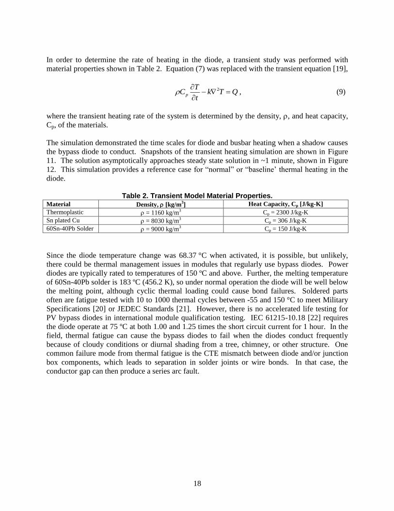
In order to determine the rate of heating in the diode, a transient study was performed with
material properties shown in Table 2. Equation (7) was replaced with the transient equation [19],
QTkt
TCp
2 , (9)
where the transient heating rate of the system is determined by the density, , and heat capacity,
Cp, of the materials.
The simulation demonstrated the time scales for diode and busbar heating when a shadow causes
the bypass diode to conduct. Snapshots of the transient heating simulation are shown in Figure
11. The solution asymptotically approaches steady state solution in ~1 minute, shown in Figure
12. This simulation provides a reference case for ―normal‖ or ―baseline’ thermal heating in the
diode.
Table 2. Transient Model Material Properties.
Material Density, [kg/m3] Heat Capacity, Cp [J/kg-K]
Thermoplastic = 1160 kg/m3 Cp = 2300 J/kg-K
Sn plated Cu = 8030 kg/m3 Cp = 306 J/kg-K
60Sn-40Pb Solder = 9000 kg/m3 Cp = 150 J/kg-K
Since the diode temperature change was 68.37 °C when activated, it is possible, but unlikely,
there could be thermal management issues in modules that regularly use bypass diodes. Power
diodes are typically rated to temperatures of 150 ºC and above. Further, the melting temperature
of 60Sn-40Pb solder is 183 ºC (456.2 K), so under normal operation the diode will be well below
the melting point, although cyclic thermal loading could cause bond failures. Soldered parts
often are fatigue tested with 10 to 1000 thermal cycles between -55 and 150 °C to meet Military
Specifications [20] or JEDEC Standards [21]. However, there is no accelerated life testing for
PV bypass diodes in international module qualification testing. IEC 61215-10.18 [22] requires
the diode operate at 75 ºC at both 1.00 and 1.25 times the short circuit current for 1 hour. In the
field, thermal fatigue can cause the bypass diodes to fail when the diodes conduct frequently
because of cloudy conditions or diurnal shading from a tree, chimney, or other structure. One
common failure mode from thermal fatigue is the CTE mismatch between diode and/or junction
box components, which leads to separation in solder joints or wire bonds. In that case, the
conductor gap can then produce a series arc fault.

19
t = 0.1 s, Tmax = 293.79 K
t = 1 s, Tmax = 299.24 K
t = 10 s, Tmax = 339.39 K
t = 50 s, Tmax = 358.63 K
Figure 11. Temperature distribution from Joule and internal heating of the diode for different simulation times.
Figure 12. Transient diode thermal model reaching steady state with thermal measurements taken at diode leads.
290
300
310
320
330
340
350
360
0 50 100 150 200
Tem
pe
ratu
re (
K)
Time (s)
Transient Response from Diode Heating in Diode Leads

20
2.3 Diode Degradation
In order to simulate corrosion and electrical degradation of the diode, contact resistance was
added to the model between the bus and the diode, shown in Figure 13. In the previous section,
there was a low voltage drop (4.3 mV) through the diode when the bypass diode was conducting
properly. This voltage drop increases as the solder bond degrades because the electrical
conductivity of 60Sn-40Pb solder is 6.5 × 10³
S/m but the electrical conductivity of air is
~5.5 × 10⁻¹⁵
S/m [23]. This analysis investigated the thermoelectrical behavior of the diode
subdomain for conductivities between that of a good solder bond to an open connection, though,
even without a catastrophic solder failure, thermal cycling can decrease the thermal conductivity
of the soldered joints [24].
Figure 13. Location of contact resistance from corrosion.
A parametric study was performed taking the conductivity of the contact resistance from air
(5.5 × 10⁻¹⁵
S/m) to solder (6.5 × 10³
S/m) and up to Cu/Sn (3.5 × 10⁷
S/m) using Equations (5)
and (6). The results are shown in Figure 14 for an assumed gap distance d = 5 m. There is a
low voltage drop from = 10 to 1 × 10⁷ S/m, but the voltage drop increases to 7.16 volts at 1
S/m. This is less than 0.02% of the electrical conductivity of solder so there would be significant
degradation of the solder joint to achieve this voltage across the gap. The dielectric strength of
air is 3000 V/mm or 3 V/m [25,26] at standard temperature and pressure (STP). When a gap
size, d, has a potential v = |v1-v2| = 3 V/m across it, air will ionize and form an arc. Therefore,
based on the voltage across the gap, the minimum safe (non-arcing) gap in microns is
μm/V3
vd , (10)
though, in the case of the actual diode, the gap will not contain pure air, but rather a combination
of outgassed organics (e.g., hydrocarbons from adhesives) and, in some modules, encapsulant
material inside the junction box. These materials and gasses will have different dielectric
strengths, and therefore will not arc at the same gap potential.
21
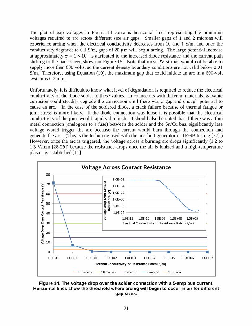
The plot of gap voltages in Figure 14 contains horizontal lines representing the minimum
voltages required to arc across different size air gaps. Smaller gaps of 1 and 2 microns will
experience arcing when the electrical conductivity decreases from 10 and 1 S/m, and once the
conductivity degrades to 0.1 S/m, gaps of 20 m will begin arcing. The large potential increase
at approximately = 1 × 10⁻⁵
is attributed to the increased diode resistance and the current path
shifting to the back sheet, shown in Figure 15. Note that most PV strings would not be able to
supply more than 600 volts, so the current density boundary conditions are not valid below 0.01
S/m. Therefore, using Equation (10), the maximum gap that could initiate an arc in a 600-volt
system is 0.2 mm.
Unfortunately, it is difficult to know what level of degradation is required to reduce the electrical
conductivity of the diode solder to these values. In connectors with different materials, galvanic
corrosion could steadily degrade the connection until there was a gap and enough potential to
cause an arc. In the case of the soldered diode, a crack failure because of thermal fatigue or
joint stress is more likely. If the diode connection was loose it is possible that the electrical
conductivity of the joint would rapidly diminish. It should also be noted that if there was a thin
metal connection (analogous to a fuse) between the solder and the Sn/Cu bus, significantly less
voltage would trigger the arc because the current would burn through the connection and
generate the arc. (This is the technique used with the arc fault generator in 1699B testing [27].)
However, once the arc is triggered, the voltage across a burning arc drops significantly (1.2 to
1.3 V/mm [28-29]) because the resistance drops once the air is ionized and a high-temperature
plasma is established [11].
Figure 14. The voltage drop over the solder connection with a 5-amp bus current. Horizontal lines show the threshold where arcing will begin to occur in air for different
gap sizes.
0
10
20
30
40
50
60
70
80
1.0E-01 1.0E+00 1.0E+01 1.0E+02 1.0E+03 1.0E+04 1.0E+05 1.0E+06 1.0E+07
Vo
ltag
e D
rop
Ove
r C
on
tact
Re
sist
ance
(V
)
Electical Conductivity of Resistance Patch (S/m)
Voltage Across Contact Resistance
20 micron 10 micron 5 micron 2 micron 1 micron
1.0E-04
1.0E-02
1.0E+00
1.0E+02
1.0E+04
1.0E+06
1.0E-15 1.0E-10 1.0E-05 1.0E+00 1.0E+05Vo
ltag
e D
rop
Ove
r C
on
tact
R
esi
stan
ce (
V)
Electical Conductivity of Resistance Patch (S/m)

22
= 1 × 10⁻³
S, d = 5 × 10⁻⁶
m, contact conductivity = /d = 200 S/m2
= 1 × 10
-5, d = 5 × 10
-6 m, contact conductivity = /d = 2 S/m
2
= 1 × 10
-7, d = 5 × 10
-6 m, contact conductivity = /d = 0.02 S/m
2
Figure 15. Transition from diode acting as a conducting path to the plastic back sheet.

23
If an arc did not form from the large voltage gap, the temperature profile would closely match
the voltage drop profile. The diode temperatures with electrical conductivities below 1 S/m
increase significantly because of i2R losses, shown in Figure 16. The /d term in Equations (5)
and (6) defines the electrical conductivity between the bus and diode, and since the electrical
conductivity is the reciprocal of electrical resistance (1/S = ), the electrical resistance and,
hence, Joule heating are linearly dependent on d and 1/.
Figure 16. The steady state temperature of the diode due to increasing ohmic losses.
375
380
385
390
395
400
405
410
415
420
425
1.0E-01 1.0E+00 1.0E+01 1.0E+02 1.0E+03 1.0E+04 1.0E+05 1.0E+06 1.0E+07
Tem
pe
ratu
re (
K)
Electical Conductivity of Resistance Patch (S/m)
Temperature from Joule Heating
1.0E+00
1.0E+02
1.0E+04
1.0E+06
1.0E+08
1.0E+10
1.0E-15 1.0E-10 1.0E-05 1.0E+00 1.0E+05
Tem
pe
ratu
re (
K)
Electical Conductivity of Resistance Patch (S/m)

24
3. PHYSICS OF ARCING
As shown above, sufficient degradation of the solder connections in PV systems will cause an
arc to initiate. The arc is a plasma column between two electrodes of opposite polarity,
established when the dielectric strength of the atmosphere is exceeded. While initially the
atmosphere is an excellent insulator, the ionized plasma is an excellent conductor and the voltage
drop across the gap decreases from 3000 V/mm to 1.2 V/mm. A diagram of the voltage drop
across the arc gap is shown in Figure 17. With the arc established, the anode and cathode drop
is relatively consistent for different electrode materials. Generally this voltage drop is 20 to 40
volts (for example, it is 23.5 V for copper, 26.5 V for steel, and 36 V for tungsten [30-31]).
Figure 17. Voltage characteristics of an arc across a gap [30,31].
The initiation and sustainment of the arc is dependent on a number of material and geometric
considerations. Stokes and Oppenlander report, ―the minimum voltage needed to maintain an arc
depends on current magnitude, gap width, and orientation of the electrodes‖ [32]. Direct current
(DC) arcs do not pass through zero current every half cycle like alternating current (AC) arcs so
they are much more difficult to extinguish. However, the arc can be extinguished with arc-
suppressing atmospheric conditions or an increasing gap distance. Unfortunately, PV arc faults
often start in coated wiring, or around organic-based adhesives and epoxies. When exposed to
the high temperatures of the arc plasma, these materials pyrolyze and release combustible
hydrocarbons that subsequently start PV fires [27]. With fire-retardant materials [33] the fire
risk can be reduced. Hastings found that DC arcs will self-extinguish when the atmospheric
conditions include flame-retardant chemistries [34]. The second option for self-extinguishing an
arc is by burning the electrodes apart from each other. The arc resistance is linearly proportional
to the arc gap for a given arc current [32]. As the gap widens, the resistance of the arc grows and
eventually breaks the plasma column.

25
3.1 Polymer Burn Times
One of the biggest hazards from PV arc faults is igniting a fire in the PV materials, which can
spread to the building. The 5000 to 7000 K arc will melt metals and quickly vaporize and burn
polymers that are in direct contact with the arc. However, it will also ignite materials that are
separated from the arc itself through radiative heating. It is difficult to estimate the time required
to burn distanced PV materials, but some researchers have developed analytical relationships
between arc wattage and burn times. In Figure 18, Hastings extrapolated surface ignition times
from References 35 and 36 and estimated burn-through times based on arc radiation power
densities. Hastings also determined an equation for burn-through times versus power density,
though empirical results varied because of the chaotic nature of arcs [34].
Figure 18. Time to surface ignition versus power density and burn-through times for different arc powers when the arc is encapsulated by the polymer sheath [34].
The power density from Joule heating is not the same as the incident arc radiation on the
materials, so the power density cannot be taken directly from the simulation. To estimate the
power in the PV arc, the voltage change during an experimental arc is multiplied by the string
current. Experimentation at SNL showed that a single string operating at 4 amps experienced
roughly a 25-volt drop in string voltage during an arc [37]. Therefore, based on the conservation
of energy, it is expected that 100 watts of radiation was generated by the arc. (This is one-third
the power required for the arc tests in UL 1699B [38], but nearly five times the arc power of
some arc fault circuit interrupter (AFCI) tests [39].) Assuming the arc is initiated at the interface
between the diode lead and busbar, there is a small gap between the arc and the plastic back
sheet. The area directly below the arc will be exposed to the greatest amount of radiation, so a
representative patch is used to calculate the incident radiation. To calculate the view factor the
arc is modeled as a semi-infinite horizontal cylinder and the patch has infinite depth, shown on
the right of Figure 19. The view factor from area A1 to area A2 is [40]
h
wF
2/tan
1 1
21
. (11)

26
The view factor is 0.041 for this geometry, meaning that 4.1% of the radiation produced by the
arc will be incident on the 1-mm subdomain of the back sheet directly below the arc. Thus, the
square (1 mm2) region below the arc will experience approximately 4.1 watts of arc radiation, or
4100 kW/m2. Based on this power density and extrapolating the data on the left side of Figure
18, the back sheet would ignite in less than 0.1 second. As the height decreases and the width
increases, the view factor and incident radiation increase, as shown in Figure 20. As expected, if
the arc was generated farther away from the plastic material it would take more time to combust.
However, if the diode was potted, the radiation view factor would be essentially 1.0 for the
encapsulant because all the radiation energy would be absorbed by the surrounding material and
ignite in less time. Thus, regardless of the geometry, materials in the vicinity of the arc fault will
burn or melt in extremely short time periods.
Figure 19. Radiation model and view factor parameters.
Figure 20. View factors for different values of w and h, given that r ≤ h.
Arc Column
Incident
Radiation
h = 3.81 mm
r A1 = semi-
infinite cylinder
w = 0.5 mm
A2 = planar surface
Back Sheet
Surface
(black body)

27
4. CONCLUSIONS
Arc faults in rooftop PV systems have caused residential and commercial building fires. Due to
the 2011 National Electrical Code standard requiring arc fault detection [41], there has been an
expanded effort to understand the root cause and behavior of series arcs in PV systems. Series
arcs result from the current bridging a conduction discontinuity in the electrical system. The
discontinuity can form in modules, inverters, connectors, disconnects, or other connections. This
study selected a bypass diode as a potential area for arcing because bypass diodes have been
known to fail and there are documented cases of arcing in junction boxes.
To determine if frequent use of the bypass diode could lead to premature failure, the Joule and
internal forward-bias heating in a diode was studied with a finite element model in COMSOL.
The study determined that there is a 68.37 °C temperature increase from diode use in
approximately 1 minute—but not enough to cause accelerated failures in diodes under normal
operating conditions occurring from shading of modules. Next, corrosion was simulated at the
diode solder connection to determine the correlation between contact resistance, gap voltage
drop, and Joule heating. The arc will only jump the gap if there is enough electrical potential to
cause the dielectric breakdown of the atmosphere between the electrodes. It was determined that
for an air atmosphere, the resistance of the solder bond would have to increase 1000 times to
create an arc across a 1-m gap. However, once the arc is formed, the high-temperature plasma
irradiates the surrounding material, igniting polymers and melting metals. A calculation using
empirical measurements found that the polymeric back sheet would ignite in less than 0.1
second.
This simulation studied the electrical and thermal behavior of one connection in a PV module.
Additional simulations and experimental tests are needed to fully characterize the arc fault
dangers in PV systems and identify how these hazards can be ameliorated or eliminated.
Further, experimental validation is required to corroborate these simulations. The physical
trends shown in this report are based on thermoelectric physics mechanisms included in the
simulations; however, the qualitative values need to be validated with experimental data.

28
5. REFERENCES
[1] H. Haeberlin, Arc Detector as an External Accessory Device for PV Inverters for Remote
Detection of Dangerous Arcs on the DC Side of PV Plants, European Photovoltaic Solar Energy
Conference Valencia, Spain 2010.
[2] L. Ji, PV Fire: Experience and Studies, International Photovoltaic Reliability Workshop II,
Tempe, AZ, July 31, 2009.
[3] P. Jackson, Target Roof PV Fire of 4-5-09, City of Bakersfield, California, Development
Services/Building Department Memorandum, April 29, 2009.
[4] J. Johnson, ―Overview of Arc-Faults and Detection Challenges,‖ Arc Fault Detection and
Mitigation Webinar, Solar ABCs, February 8, 2010. Available from:
http://www.solarabcs.org/about/publications/meeting_presentations_minutes/2011/02/pdfs/Johns
on_Presentation.pdf
[5] S. Kurtz, J. Granata, and M. Quintana, Photovoltaic-Reliability R&D Toward a Solar-
Powered World, Society of Photographic Instrumentation Engineers (SPIE) Solar Energy &
Technology Conference, San Diego, California, August 2-6, 2009.
[6] A.M. Ricaud and R.C. Petersen, Environmental stress tests: acceleration of corrosion, in
Proceedings of the 8th European Commission PV Solar Energy Conference, Florence, Italy,
1988, pp. 549-553.
7] T.J. McMahon and G.J. Jorgensen, Adhesion and thin-film module reliability, in Proceedings
of the 4th World Conference on PV Energy Conversion, Waikoloa, Hawaii, USA, 2006, pp.
2062-2065.
[8] G.J. Jorgensen, K.M. Terwilliger, J.A. DelCueto, S.H. Glick, M.D. Kempe, J.W. Pankow,
F.J. Pern, and T.J. McMahon, Moisture transport, adhesion, and corrosion protection of PV
module packaging materials, Solar Energy Materials & Solar Cells, Vol. 90, pp. 2739-2775,
2006.
[9] C. Whitaker, PG&E’s perspectives on module reliability, in NREL/DOE Photovoltaic
Performance and Reliability Workshop.
[10] J. Johnson, J. Strauch, S. Kuszmaul, D. Schoenwald, and W. Bower, Characterizing PV
Arcing Conditions with Impedance Spectroscopy and Frequency Response Analysis, 26th
European Photovoltaic Solar Energy Conference and Exhibition, Hamburg, Germany, 2011.
[11] J. Strauch, M. Quintana, J. Granata, S. Kuszmaul, and J. Johnson, PV Module Arc Fault
Modeling and Analysis,‖ Photovoltaic Module Reliability Workshop, Golden, CO, February
2011. Presentation available from: http://www1.eere.energy.gov/solar/pdfs/pvmrw2011_30_csi
_strauch.pdf

29
[12] G. TamizhMani, B. Li, T. Arends, J. Kuitche, B. Raghuraman, W. Shisler, K. Farnsworth, J.
Gonzales, A. Voropayev, and P. Symanski, Failure analysis of design qualification testing: 2007
VS. 2005, 33rd IEEE Photovoltaic Specialists Conference, May 11-16, 2008. DOI:
10.1109/PVSC.2008.4922768.
[13] A. Schlumberger, A. Kreutzmann, Brennendes Problem – Schadhafte BP-Module können
Feuer entfachen, Photon, August 2006, pp. 104-106 (in German).
[14] J.W. Bishop, Computer Simulation of the Effects of Electrical Mismatches in Photovoltaic
Cell Interconnection Circuits, Solar Cells, Vol. 25, pp. 73-89, 1988.
[15] S.A. Fahrenbruch, Solar bypass diodes: Then and now, Solar, A PV Management Magazine,
Vol. VI, pp. 21-26, 2010.
[16] D. Roche, H. Outhred, and R. John Kaye, Analysis and Control of Mismatch Power Loss in
Photovoltaic Arrays, Progress in Photovoltaics: Research and Applications, Vol. 3, pp. 115-127,
1995.
[17] T. Zgonena, L. Ji, and D. Dini, Photovoltaic DC Arc-Fault Circuit Protection and UL
Subject 1699B, Photovoltaic Module Reliability Workshop, Golden, CO, February 2011.
Presentation available from: http://www1.eere.energy.gov/solar/pdfs/pvmrw2011_p06_gen_ji.
[18] M.C. Alonso García, J.L. Balenzategui, Estimation of photovoltaic module yearly
temperature and performance based on Nominal Operation Cell Temperature calculations,
Renewable Energy, vol. 29, issue 12, October 2004, pp. 1997-2010.
[19] F.P. Incropera and D.P. DeWitt, Introduction to Heat Transfer, 4th
Ed., John Wiley & Sons,
New York, NY, 2002.
[20] MIL-STD-883G, Department of Defense Test Method Standard: Microcircuits, Test Method
1010, United States Department of Defense, February 28, 2006.
[21] JEDEC Standard JESD22-A104, Temperature Cycling, May 2005.
[22] International Electrotechnical Commission, International Standard 61215, 2nd
Ed.,
Crystalline silicon terrestrial photovoltaic (PV) modules – Design qualification and type
approval, 2005.
[23] S.D. Pawar, P. Murugavel, and D.M. Lal, Effect of relative humidity and sea level pressure
on electrical conductivity of air over Indian Ocean, Journal of Geophysical Research, Vol. 114,
D02205, 2009.
[24] F. Guo, J.G. Lee, T. Hogan, and K.N. Subramanian, Electrical conductivity changes in bulk
Sn, and eutectic Sn-Ag in bulk and in joints, from aging and thermal shock, Journal of Materials
Research, Vol. 20, Issue 2, pp. 364-374, 2005.

30
[25] P.A. Tipler, College Physics, Worth, p. 467, 1987.
[26] J.S. Rigden, Macmillan Encyclopedia of Physics, Simon & Schuster, pp. 353, 1996.
[27] D. Dini, P. Brazis, and K.-H. Yen, Development of Arc-Fault Circuit-Interrupter
Requirements for Photovoltaic Systems, 37th
Photovoltaic Specialists Conference, Seattle, WA,
June 19-24, 2011.
[28] T.E. Browne, The electric arc as circuit element, J. Electrochem. Soc., Vol. 102, No. 27,
1955. DOI:10.1149/1.2429985.
[29] A.P. Strom, Long 60-cycle arcs in air, Trans. Amer. Inst. Elect. Eng., Vol. 65, pp. 113-117,
1946.
[30] V.P. Ignatko, Electric characteristics of ac open heavy-current arcs,‖ in Proc. 3rd Int. Symp.
Switching Arc Phenom., pp. 98-102, 1977.
[31] R.F. Ammerman, T. Gammon, P.K. Sen, and J.P. Nelson, DC-Arc Models and Incident-
Energy Calculations, IEEE Transactions on Industry Applications, Vol. 46, No. 5, pp.1810-1819,
September-October 2010. DOI: 10.1109/TIA.2010.2057497.
[32] A.D. Stokes and W.T. Oppenlander, Electric arcs in open air, J. Phys. D, Appl. Phys., Vol.
24, No. 1, pp. 26-35, January 1991.
[33] A.B. Morgan and M. Bundy, Cone calorimeter analysis of UL-94 V-rated plastics, Fire and
Materials, Vol. 31, pp. 257-283, 2007. DOI: 10.1002/fam.937.
[34] J.K. Hastings, M.A. Juds, C.J. Luebke, and B. Pahl, A study of ignition time for materials
exposed to dc arcing in PV systems, 37th
Photovoltaic Specialists Conference, Seattle, WA, June
19-24, 2011.
[35] V. Babrauskas, Ignition Handbook, Fire Science Publishers, 2003.
[36] V. Babrauskas, and I. Wetterland, Comparative Data from LIFT and Cone Calorimeter
Tests on 6 Products, Including Flame Flux Measurements, SP Report 1999:14, Swedish National
Testing and Research Institute, Borås.
[37] J. Johnson, B. Pahl, C.J. Luebke, T. Pier, T. Miller, J. Strauch, S. Kuszmaul, and W. Bower,
Photovoltaic DC arc fault detector testing at Sandia National Laboratories, 37th Photovoltaic
Specialists Conference, Seattle, WA, June 19-24, 2011.
[38] Underwriters Laboratories (UL) Subject 1699B, Outline of Investigation for Photovoltaic
(PV) DC Arc-Fault Circuit Protection, April 29, 2011.

31
[39] C.J. Luebke, T. Pier, B. Pahl, D. Breig, and J. Zuercher, Field Test Results of DC Arc Fault
Detection on Residential and Utility Scale PV Arrays, 37th Photovoltaic Specialists Conference,
Seattle, WA, June 19-24, 2011.
[40] M.F. Modest, Radiative heat transfer, 2nd Ed., Academic Press, San Diego, CA, 2003.
[41] National Electrical Code, 2011 Edition, NFPA70, National Fire Protection Association,
Batterymarch, MA.
32
DISTRIBUTION
External distribution
1 U.S. Department of Energy
Solar Energy Technology Program
Attn: Kevin Lynn
950 L’Enfant Plaza
Washington, DC 20585
Internal distribution
1 MS0352 Jay Johnson 01718
1 MS0352 W. Kent Schubert 01718
1 MS0734 Ward I. Bower 06111
1 MS0951 Michael Quintana 06124
1 MS0951 Bruce King 06112
1 MS1033 Sigifredo Gonzalez 06112
1 MS1033 Abraham Ellis 06112
1 MS1033 Jennifer E. Granata 06112
1 MS1033 Charles J. Hanley 06112
1 MS1078 Wahid L. Hermina 01710
1 MS1079 Gilbert V. Herrera 01700
1 MS1082 Anthony L. Lentine 01727
1 MS1104 Rush D. Robinett III 06110
1 MS1108 Ross Guttromson 06113
1 MS0359 D. Chavez, LDRD Office 01911
1 MS0899 RIM-Reports Management 09532 (electronic copy)