ELECTRICAL AND MECHANICAL PROPERTIES OF MWCNT FILLED ...
57
University of Kentucky University of Kentucky UKnowledge UKnowledge University of Kentucky Master's Theses Graduate School 2009 ELECTRICAL AND MECHANICAL PROPERTIES OF MWCNT FILLED ELECTRICAL AND MECHANICAL PROPERTIES OF MWCNT FILLED CONDUCTIVE ADHESIVES ON LEAD FREE SURFACE FINISHED CONDUCTIVE ADHESIVES ON LEAD FREE SURFACE FINISHED PCB's. PCB's. Keerthi Varma Mantena University of Kentucky, [email protected] Right click to open a feedback form in a new tab to let us know how this document benefits you. Right click to open a feedback form in a new tab to let us know how this document benefits you. Recommended Citation Recommended Citation Mantena, Keerthi Varma, "ELECTRICAL AND MECHANICAL PROPERTIES OF MWCNT FILLED CONDUCTIVE ADHESIVES ON LEAD FREE SURFACE FINISHED PCB's." (2009). University of Kentucky Master's Theses. 613. https://uknowledge.uky.edu/gradschool_theses/613 This Thesis is brought to you for free and open access by the Graduate School at UKnowledge. It has been accepted for inclusion in University of Kentucky Master's Theses by an authorized administrator of UKnowledge. For more information, please contact [email protected].
Transcript of ELECTRICAL AND MECHANICAL PROPERTIES OF MWCNT FILLED ...

University of Kentucky University of Kentucky
UKnowledge UKnowledge
University of Kentucky Master's Theses Graduate School
2009
ELECTRICAL AND MECHANICAL PROPERTIES OF MWCNT FILLED ELECTRICAL AND MECHANICAL PROPERTIES OF MWCNT FILLED
CONDUCTIVE ADHESIVES ON LEAD FREE SURFACE FINISHED CONDUCTIVE ADHESIVES ON LEAD FREE SURFACE FINISHED
PCB's. PCB's.
Keerthi Varma Mantena University of Kentucky, [email protected]
Right click to open a feedback form in a new tab to let us know how this document benefits you. Right click to open a feedback form in a new tab to let us know how this document benefits you.
Recommended Citation Recommended Citation Mantena, Keerthi Varma, "ELECTRICAL AND MECHANICAL PROPERTIES OF MWCNT FILLED CONDUCTIVE ADHESIVES ON LEAD FREE SURFACE FINISHED PCB's." (2009). University of Kentucky Master's Theses. 613. https://uknowledge.uky.edu/gradschool_theses/613
This Thesis is brought to you for free and open access by the Graduate School at UKnowledge. It has been accepted for inclusion in University of Kentucky Master's Theses by an authorized administrator of UKnowledge. For more information, please contact [email protected].

ABSTRACT OF THESIS
ELECTRICAL AND MECHANICAL PROPERTIES OF MWCNT FILLED CONDUCTIVE ADHESIVES ON LEAD FREE SURFACE FINISHED PCB’s.
Electrically conductive adhesives (ECA) are an alternative to tin/lead solders for attaching Surface Mount Devices (SMD) in electronic assemblies. ECAs are mixtures of a polymer binder (for adhesion) and conductive filler (for electrical conductivity). They bring more conductivity, higher strength, less weight and longer durability than metal alloys. ECAs can offer numerous advantages such as fewer processing steps, lower processing temperature and fine pitch capability. Multi walled carbon nanotubes (MWCNT) were used as conductive fillers in this research because of their novel electronic and mechanical properties.
The high aspect ratio of the nanotubes makes it possible to percolate at low loadings to obtain good electrical and mechanical properties. Replacing the metal filler with CNTs in the adhesive made the ECA light weight, corrosion resistant, reduced processing temperature, lead free, electrically conductive and high mechanical strength. The MWCNTs at different loadings were mixed with epoxy and epoxy: heloxy to form a composite mixture. Different loadings, additives and mixing methods were used to obtain good electrical and mechanical properties and pot life. Pressure dispensing, screen and stencil printing were the processing techniques used for making the samples. The volume resistivity, contact resistance, die shear and lap shear tests were conducted on different surface finished Printed Circuit Boards (PCB) like silver, tin and Electro less Nickel Immersion Gold (ENIG). The results are summarized and compared with traditional methods. KEYWORDS: Carbon nanotubes(CNTs), Electrically conductive adhesives(ECAs),Multi walled carbon nanotubes (MWCNTs), Printed Circuit Boards (PCB),epoxy, heloxy.
Keerthi Varma Mantena
7/17/2009

ELECTRICAL AND MECHANICAL PROPERTIES OF MWCNT FILLED CONDUCTIVE ADHESIVES ON LEAD FREE SURFACE FINISHED PCB’s.
By
Keerthi Varma Mantena
Director of Thesis
Dr.Janet K Lumpp
Dr.Stephen Gedney
Director of Graduate Studies
(Date)
07/17/2009

RULES FOR THE USE OF THESIS
Unpublished thesis submitted for the Master’s degree and deposited in the University of
Kentucky Library are as a rule open for inspection, but are to be used only with due
regard to the rights of the authors. Bibliographical references may be noted, but
quotations or summaries of parts may be published only with the permission of the
author, and with the usual scholarly acknowledgments.
Extensive copying or publication of the dissertation in whole or in part also requires the
consent of the Dean of the Graduate School of the University of Kentucky.
A library that borrows this dissertation for use by its patrons is expected to secure the
signature of each user.
Name Date
________________________________________________________________
________________________________________________________________
________________________________________________________________
________________________________________________________________
________________________________________________________________
________________________________________________________________
________________________________________________________________
________________________________________________________________
________________________________________________________________
________________________________________________________________

THESIS
Keerthi Varma Mantena
The Graduate School
University of Kentucky
2009

ELECTRICAL AND MECHANICAL PROPERTIES OF MWCNT FILLED CONDUCTIVE ADHESIVES ON LEAD FREE SURFACE FINISHED PCB’s.
THESIS
A thesis submitted in partial fulfillment of the requirements for the degree of “Master of Science in Electrical Engineering in the College of Engineering” at the
University of Kentucky
By
Keerthi varma Mantena
Lexington, Kentucky
Director: Dr. Janet K Lumpp, Professor
Electrical and Computer Engineering
Lexington, Kentucky
2008
Copyright ©
Keerthi Varma Mantena 2009

DEDICATION
To My Parents and Family

iii
ACKNOWLEDGEMENTS
I would like to take this opportunity to express my sincere thanks and heartfelt
gratitude for my advisor and thesis chair Dr Janet K. Lumpp for her guidance, support
and continuous encouragement throughout my thesis. I would also like to thank Dr. Jing
Li for training and passing on his knowledge on this subject to me.
I would also like to thank Dr. Mark Meier at Center for Applied Energy Research
(CAER) , university of Kentucky for supplying us with the material which was needed
for the thesis. I wish to thank Mr. Larry Rice for his help in SEM micrographs. Most
importantly, I extend my appreciation to Naveen Velicheti, Midhun Jasti and Poojitha
Sirigiri for their incessant aid in the lab.
I owe my sincere appreciation to my family, friends, and relatives, who have
supported, encouraged, guided and loved me throughout my life. Most importantly I
would like to thank my wife, Richa, for her support and encouragement in my life.
Last I would like to thank my thesis committee members Dr. Yuan Liao and Dr.
Jinshan Li for their time and consideration.

iv
Contents
ACKNOWLEDGEMENTS………………………………………………………….. iii
List of tables………………………………………………………………………………vi
List of Figures…………………………………………………………………………....vii
Chapter 1 Introduction ........................................................................................................ 1
Chapter 2 Background…………………………………………………………………….3
2.1 Conductive Adhesives ............................................................................................. 3
2.1.1 Isotropic and Anisotropic Conductive Adhesives ............................................. 4
2.1.2 Percolation and Conductivity in ICA ................................................................ 5
2.2 Carbon Nanotubes ....................................................................................................
2.2.1 Geometry of Carbon nanotubes……………………………………………….6
6
2.2.2 Single walled nanotubes (SWNTs)……………………………………………8
2.3 Multi walled Carbon Nanotubes (MWCNTs)…………………………………...9
2.2.4 Properties of Carbon nanotubes……………………………………………….9
2.3 Different Surface finishes of Printable Circuit Boards (PCBs)…………………..10
2.3.1 Electroless Nickel Immersion Gold………………………………………….10
2.3.2 Immersion Tin………………………………………………………………..11
2.3.3 Immersion Silver……………………………………………………………..11
Chapter 3 MWNT Epoxy and Epoxy/Heloxy Composite Preparation…………….... 12
3.1 Materials ................................................................................................................ 12
3.2 MWCNT-Epoxy composite preparation...………………………………………..12
3.3 SMWCNT-Epoxy composite preparation…………...……………………………13
3.4 MWCNT-epoxy: Heloxy composite preparation ………………………….……..14

v
Chapter 4 Experimental Setup ………………………………………….….………..14
4.2 Contact Resistance Measurement…………………………………………….......17
4.1 Volume Resistivity Measurement………………………………………..…..…..14
4.3 Lap Shear Strength Measurement ……………………………………………….18
4.4 Die shear Test Measurement……………………………………………………..19
4.5 Aging Experiments…………………….…………………………………………21
Chapter 5 Results and Discussion……………….……………………………………….21
5.1 Volume resistivity Results…………….…….…………………………………….21
5.1.1 MWCNT Loadings with Epoxy composite vs. Volume Resistivity…..…….21
5.1.2 SMWCNT Loadings with Epoxy composite vs. Volume Resistivity………..22
5.1.3 MWCNT Loadings with Epoxy/Heloxy composite vs. Volume Resistivity…25
5.2 Contact Resistance Results and Discussion……………………………………....26
5.2.1 Contact resistance results for MWCNT epoxy composite…………………...26
5.2.2 Contact resistance results for MWCNT epoxy: heloxy composite……….….28
5.3 Lap shear Results and Discussions………………………………………………32
5.4 Die Shear Results and Discussion………………………………………………...37
5.5 Aging Experiments Results and Discussion……………………………………...37
Chapter 6 Conclusion and Future Work………………………………………………....40
References……………………………………………………………………………….42
Vita………………………………………………………………………………………44

vi
List of Tables Table 1:
.
Measured Volume resistivity for epoxy/MWNT composites for Different
MWNT loadings ……………………………………………………………………….. 22
Table 2:
...................................................................................................
Contact resistance on different surface finished PCBs for different MWNT
(wt%)-Epoxy composite 27

vii
List of Figures
Fig 1: Conduction Mechanism in conductive adhesives …...…………………………..…5
Figure 2: Unrolled hexagonal lattice of a carbon nanotube…………………….………....7
Figure 3: Three distinctive arrangements of carbon in SWNTs…………………….….…7
Fig 4: Single walled and Multi walled Carbon Nanotubes………………………….…....8
Figure 5: Scanned Electron Microscopic image of a shatter milled MWCNT……….....13
Figure 6: Volume Resistivity Pattern …………………………………………………....15
Figure 7: Schematic of four point probe ……………………………………………..….16
Figure 8: Contact resistance Measurement test board……………………………….......17
Figure 9: Lap shear test sample……………………………………………………….…19
Figure 10: Schematic of die shear test sample………………………………………......20
Figure 11: Average Volume resistivity vs. weight percentage of MWNT in Epoxy
Mixtures………………………………………………………………………………….23
Figure 12: Average volume resistivity vs. weight percentage of SMWCNTs in Epoxy
mixture………………………………………………………………………………...…24
Figure 13: Average volume resistivity versus Epoxy to Heloxy ratio and weight
percentage of MWCNT in Epoxy-Heloxy mixture……………………………………...25
Figure 14: Average Contact resistance on different surface finished PCBs with 8wt%
MWCNT loading and varying epoxy-Heloxy ratios………………………………….…29
Figure 15: Average Contact resistance on different surface finished PCBs with 12wt%
MWCNT loading and varying epoxy-Heloxy ratios……………………………….…....30
Figure 16: Average Contact resistance on different surface finished PCBs with 14wt%
MWCNT loading and varying Epoxy-Heloxy ratios……………………………….…..31
Figure 17: Lap shear Strength for different MWNT loadings on Gold, Silver and Tin with
Epoxy composite…………………………………………………………………….….33
Figure 18: Lap shear Strength for different MWNT loadings on Gold with different
Epoxy: Heloxy composite ratio………………………………………………………....34
Figure 19: Lap shear Strength for different MWCNT loadings on Silver with different
Epoxy: Heloxy composite ratio………………………………………………………....35
viii
Figure 20: Lap shear Strength for different MWCNT loadings on Tin with different
Epoxy: Heloxy composite ratio………………………………………………………...36
Figure 21: Die shear Strength for different MWCNT loadings on Gold, Silver, and Tin
with Epoxy composite…………………………………………………………………..38
Figure 22: Variation of volume resistivity with aging experiments on 12% MWCNT/
Epoxy: heloxy composite……………………………………………………………....39

1
Chapter 1 Introduction
Lead based solder materials have been in use for the interconnection of electronic
components on printed circuit boards (PCBs) for a long time now. As the environmental
awareness in increasing, there is a great deal of pressure on the industry to eliminate or
try to reduce the usage of lead. The policies and legislations have been proposed
worldwide to ban and reduce the use of lead in solders through RoHS, and the United
States is also taking the restrictions seriously. There has been a great effort with in the
industry to develop lead-free and environment friendly solder materials to replace the
lead-based solders.
An alternative to the lead based solder are the lead free electrically conductive
adhesives (ECAs). ECAs consist of polymer binder which provides mechanical strength,
and conductive fillers, that offer electrical conduction. ECAs provide environment
friendly solution for interconnection in electronic applications. ECAs also have some
potential advantages over the conventional solder techniques which include low
temperature processing , finer pitch and simple processing [1][2]. From these the ECAs
are considered as the next generation interconnection materials for electronic packaging.
This interconnection technology is relatively new when compared to other technologies
so it does have some limitations and drawbacks. The reliability issues that include limited
impact resistance [3], increased contact resistance and weak mechanical strength in some
climatic conditions [4] [5] are some of the major drawbacks that are preventing ECAs
from replacing the solder in certain electrical applications. It is necessary to understand
the mechanisms underlying these problems, and to improve the electrical properties of
the conductive adhesives before ECAs can be widely used as solder replacement.
Integrated chip packaging is the first level packaging which provides mechanical
strength, environment protection, heat dissipation and electrical connections for the
semiconductor devices. The second level packaging is system level packaging which
provides interconnection of the devices on the system level board as well mechanical
support and heat dissipation for the system. The important package interconnection
technologies presently in the market are wire bonding, flip chip bonding and tape
automated bonding [6].
2
The IC packaging processes make individual electrical components ready to be
handled; Printed Wiring Assembly processes integrate different electrical components
into fully functional units. The two major PWB assembly technologies are through-hole
assembly and surface mount assembly. In through assembly, leads of the components are
inserted into the conducting plated through holes and soldered on the back side of the
PWB. Where as in surface mount assemble the components can be placed on either side
of the board and soldered. Due to the fact that surface mount assembly utilizes both sides
of the board and size of surface mount components is usually smaller than comparable
through-hole components, surface mount assembly has grown in popularity [6].
In this thesis, we focused on the electrical and mechanical properties of carbon
nanotube adhesives on the commercially available surface finishes in the market. We also
modified the adhesive by using a heloxy, which is a viscosity modifier. We tested this
composite in five different variations on all the three surface finishes gold, silver and tin.
Replacing the MWCNTs with metal fillers have the advantages of being lead free,
resistant to corrosion, light weight and good mechanical strength.
3
Chapter 2 Background
2.1 Conductive adhesives
Electrically conductive adhesive (ECA) technology is one of the lead free
alternatives to solder technology. ECAs consist of a polymer binder and conductive filler.
The polymer based adhesives are widely used in the industry. They are used as insulators
due to their excellent dielectric properties. Conductive filler particles are mixed into the
polymer adhesive to provide electrical continuity. Metal filled isotropic conductive
adhesives were commercially available in the market even before RoHS. ECAs can be
classified as thermoplastic or thermosetting, based on their physical properties upon
curing. The two main classifications of ECAs are isotropic conductive adhesive (ICA)
and anisotropic conductive adhesive (ACA).
ICAs can be either thermoplastic or thermosetting. Thermoplastics have a long
linear molecular structure which gives them the ability to melt even after curing when
heated to a particular melting point without altering their intrinsic properties[b]. They are
based on conductive filler particles mixed in a solvent and dispersed in a polymer matrix.
Thermoplastic adhesives have unlimited shelf life at room temperature. Thermoplastic
adhesives are rework able [7]. One main disadvantage is it has a longer curing time when
compared to most of thermosetting adhesives [8].
Thermosets have a three dimensional polymer structure. Thermosets undergo
chemical reactions and form chemical cross links between the polymer chains. Due to
these they resist deformation even at very high temperatures. Most of the thermosets do
not require solvents. Due to the reduced use of solvents, there is a minimum possibility of
formation of bubbles and voids due to emissions during curing. The main drawbacks of
thermosets are limited shelf life and poor rework ability.
ECAs can offer numerous advantages such as fewer processing steps which
reduce processing cost, lower processing temperature which makes the use of heat-
sensitive and low cost substrate possible, and fine pitch capability. The main limitations
of the ICA technology are lower conductivity, unstable contact resistance with non-noble
metal finished components, and poor mechanical impact performance [9].
4
2.1.1 Isotropic and Anisotropic Conductive Adhesives
Isotropic conductive adhesive
Isotropic conductive adhesives consist of polymer resin such as epoxy and
conductive fillers particles such as silver flakes. Most of the commercial ICAs are based
on thermosetting resins [10]. The most common binders are thermoset epoxies due to
their properties, such as excellent adhesive strength, good chemical and corrosion
resistances and low cost, while thermoplastics are usually added to allow softening and
rework under moderate heat [10]. Most commonly used conductive fillers are silver,
gold, nickel, copper and carbon in various sizes and shapes. The conductive fillers
provide the composite with electrical conductivity through contact between the
conductive particles. Silver flakes are the most commonly used conductive fillers because
of the high conductivity, simple process and the maximum contact with flakes. Nickel-
and copper-based conductive adhesives generally do not have good resistance stability,
because both nickel and copper are easily oxidized. Even with antioxidants, copper-based
conductive adhesives show an increase in bulk resistivity after aging, especially under
high-temperature and -humidity conditions. The conductive fillers in the ICA composite
make contact with each other and form a conductive path to provide electrical
conductivity. To ensure good electrical conductivity the volume fraction loading of the
conductive filler particles must be higher than the percolation threshold. The conductive
filler provides the electrical conductivity and the polymer resin gives the mechanical
strength between the component and the substrate. An increase in loading will result in
better electrical conductivity; on the other end it decreases the mechanical strength of the
polymer resin. In a typical ICA the volume fraction loading conductive fillers is about
25% to 30% [11]. For silver the corresponding weight percent is 78% to 82%.
Anisotropic conductive adhesive
Anisotropic conductive adhesives are pastes or films of thermoplastics. The
volume fraction of filler in ACAs is 0.5% to 5% which is far below the percolation

5
threshold, thus there is no continuous electrically conductive path in ACAs before
bonding. The component terminations are pressed against the corresponding pads on the
substrate in order to compress the conductive particles trapped between the component
terminations and substrate pads in order to form the electrically conductive path during
bonding. ACAs require high heat and pressure during the bonding process. After bonding
the ACAs become electrically conductive in one direction and remain insulating the other
direction. The use of ECAs is a no-clean process, since there is no flux involved in the
assembly process, The ECAs work well with all types of board finishes [12].
2.1.2 Percolation and Conductivity in ICA
There are two conductive pathways for isotropic conductive adhesives as shown
in Figure 1. One is genuine conduction, caused by particle-to-particle contact within the
polymer matrix. The other is percolation, which involves electron transport brought about
by quantum-mechanical electron tunneling between particles close enough to allow
dielectric breakdown of the matrix [12]. The conductivity of isotropic conductive
adhesives depends on uniform dispersion of the filler particles to form a conductive path
in the polymer matrix. Most of the traditional metal filled conductive adhesives require
25 to 30% volume fraction to overcome the percolation threshold and ensure electrical
conductivity [11]. However for less than 1% volume fraction of carbon black in the resin
can cause electrical conduction. The largest reduction in volume resistivity is observed
at0.25 wt% which means the percolation threshold is less than 0.25 wt% [20].
1(a) Particle-to-particle 1(b) electron tunneling
Fig 1: Conduction Mechanism in conductive adhesives [12]

6
2.2 Carbon Nanotubes
Carbon nanotubes are added as conductive fillers in the ECA. High aspect ratio, large
surface area multiwall carbon nanotubes (MWCNTs) have the potential as ICA filler
particles to reach the percolation threshold with small volume fraction loading compared
to silver filled adhesives. The MWCNT used in the present study have aspect ratios of
2500:1.
Carbon nanotubes are molecular-scale tubes of graphitic carbon with outstanding
properties. They are among the stiffest and strongest fibers known, and have remarkable
electronic properties and many other unique characteristics. They are chemically stable,
mechanically very storing and conduct electricity. For this reason they open up new
perspectives for various applications, such as nanotransistors in circuits, field emission
displays, artificial muscles or added reinforcements in alloys. They exhibit extraordinary
strength and unique electrical properties and are efficient conductors of heat [13].
2.2.1 Geometry of Carbon nanotubes
An ideal nanotube is a hexagonal network of carbon atoms that has been rolled up to
make a seamless cylinder. Just nanometer across, the cylinders can be tens of microns
long, and each end is "capped" with half of a fullerene molecule. Single-wall nanotubes
have a fundamental cylindrical structure, and these form the building blocks of both
multi-wall nanotubes and the ordered arrays of single-wall nanotubes called ropes. The
atoms in CNT are arranged in hexagons, the same arrangement as in graphite. In graphite
the hexagons lie in flat sheets on top of each other while in a nanotube, the sheet is rolled
into a tube [14].

7
Figure 2: Unrolled hexagonal lattice of a carbon nanotube [14].
.There are three unique geometries of carbon nanotubes. They are also referred to
as flavors. The three flavors are armchair, zigzag, and chiral [e.g. zigzag (n, 0); armchair
(n, n); and chiral (n, m)]. These flavors can be classified by how the carbon sheet is
wrapped into a tube as shown in the below figure 3.
Figure 3: Three distinctive arrangements of carbon in SWNTs [14].
8
Shown in Figure 3 is a (5, 5) armchair nanotube (top), a (9, 0) zigzag nanotube
(middle) and a (10, 5) chiral nanotube. The diameter of the nanotubes depends on the
values of n and m [14].
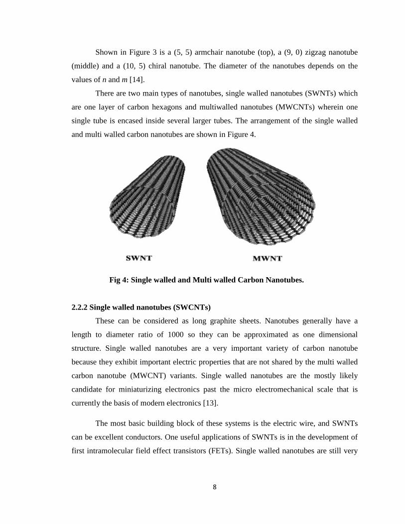
There are two main types of nanotubes, single walled nanotubes (SWNTs) which
are one layer of carbon hexagons and multiwalled nanotubes (MWCNTs) wherein one
single tube is encased inside several larger tubes. The arrangement of the single walled
and multi walled carbon nanotubes are shown in Figure 4.
Fig 4: Single walled and Multi walled Carbon Nanotubes.
2.2.2 Single walled nanotubes (SWCNTs)
These can be considered as long graphite sheets. Nanotubes generally have a
length to diameter ratio of 1000 so they can be approximated as one dimensional
structure. Single walled nanotubes are a very important variety of carbon nanotube
because they exhibit important electric properties that are not shared by the multi walled
carbon nanotube (MWCNT) variants. Single walled nanotubes are the mostly likely
candidate for miniaturizing electronics past the micro electromechanical scale that is
currently the basis of modern electronics [13].
The most basic building block of these systems is the electric wire, and SWNTs
can be excellent conductors. One useful applications of SWNTs is in the development of
first intramolecular field effect transistors (FETs). Single walled nanotubes are still very

9
expensive to produce, and the development of more affordable synthesis techniques is
vital to the future of carbon nanotube technology [13].
2.2.3 Multi walled Carbon Nanotubes (MWCNTs)
Multi walled nanotubes consist of multiple layers of graphite rolled in on them to
form a tube shape. These can be considered as a collection of concentric SWNTs with
different diameters, lengths and properties. Multi walled nanotubes consist of multiple
layers of graphite rolled in on them to form a tube shape. The distance between each
layer is approximately 0.34 nm, slightly larger than the interlayer distance of graphite
sheets and the layers are coupled to each other through van der Waals forces [13].
High aspect ratio, large surface area multiwall carbon nanotubes (MWCNTs)
have the potential as ICA filler particles to reach the percolation threshold with small
volume fraction loading. The MWCNT used in the present study have aspect ratios of
2500:1. MWCNT are electrically conductive independent of synthesis method and have
extremely high strength to weight ratio offering the potential to improve the stiffness of
the polymer matrix. The unique mechanical and electronic properties of multiwall
nanotubes are proving to be a rich source of new physics and could also lead to new
applications in materials and devices.
2.2.4 Properties of Carbon nanotubes
Multiwall carbon nanotubes (MWCNT) are metallic, whereas single wall carbon
nanotubes (SWCNT) may be metallic or semiconducting depending on the chirality of
the grapheme walls. The measured electrical conductivity of metallic carbon nanotubes is
in the order of 104 S/cm [15]. The thermal conductivity of carbon nanotubes at room
temperature can be as high as 6600 W/mK [16]. Carbon nanotubes have a Young's
modulus of approximately 1 TPa and a maximum tensile strength of nearly 30 GPa [17].
The density of MWCNT is 2.6 g/cm3 and the density of SWCNT range from 1.33 g/cm3
to 1.40 g/cm3 depending on the chirality [18]. Carbon nanotubes are the strongest and
stiffest materials on earth, in terms of tensile strength and elastic modulus respectively.

10
Blending the extreme properties of carbon nanotubes into polymer matrix composites has
tremendous potential for increasing strength, strength to weight ratio, thermal
conductivity and electrical conductivity of the bulk polymer.
2.3 Different Surface Finishes of Printed Circuit Boards (PCBs)
RoHS directive impacts not only the solder alloys that one is permitted to use, but
also many other aspects of the electronics assembly process, including the selection and
compatibility of board fabrication materials. The selection of an appropriate surface
finish plays an important role in printed circuit board manufacturing to ensure solder
ability, reliability and high yield assembly of through whole and surface mount products.
Surface finish is applied to copper pads and exposed traces for protection during storage
and transportation from the time of board manufactured to the time the circuit is
assembled. Therefore, the surface finish must maintain the solder ability of the board and
protect the metal areas from contamination and oxidation, thus increasing its shelf-life.
PCB Surface Finishes vary in price, availability, shelf life, reliability and assembly
processing. While each finish has its own benefits, in most cases, the process, product or
environment will dictate the surface finish that is best suited for the application. All
Printed Circuit Boards (PCBs) have copper finishes on their surface. If the copper finish
is left unprotected the copper will oxidize and deteriorate, there are various protective
finishes available. The most prevalent are; Hot Air Solder Leveling (HASL), Organic
Solder Preservative (OSP), Electroless-Nickel Immersion Gold (ENIG), Immersion
Silver and Immersion Tin. We carried out the tests on Immersion Silver, Immersion Tin
and Electro less-Nickel Immersion Gold [19].
2.3.1 Electroless Nickel Immersion Gold
ENIG coatings have been used with great success on many boards despite the high per
unit cost. It has a flat surface and excellent solder ability. The main drawback is that the
electroless nickel layer is brittle and has been found to break up during mechanical stress.
This effect is known in the industry as 'black pad' or 'mudflat cracking'.

11
The advantage of ENIG is excellent solder ability, coplanar - flat surface,
excellent shelf life and withstands multiple reflows. The disadvantages are higher cost,
'black pad' issue, manufacture process uses cyanide and other hazardous chemicals [19].
2.3.2 Immersion Tin
Immersion tin is a newer alternative surface finish, with many similar characteristics to
its silver counterpart. However, there are major health and safety issues to consider. It is
mainly used in Europe and Asia whilst its use in the US is restricted due to the concern
over the thiourea used in tin solution (a suspected carcinogen).
The advantages of immersion tin are good solder ability, flat surface area and
relatively low cost. The disadvantages are health and safety concerns and limited number
of heat cycles [19].
2.3.3 Immersion Silver
Immersion silver is a relatively recent addition to the PCB finish. Its main use has been in
Asia and is gaining popularity in North America. Europe now has an emerging market.
During the soldering process the silver layer dissolves into the solder joint leaving a
tin/lead/silver alloy on the copper which provides very reliable solder joints for Ball Grid
Array (BGA) packages. The contrasting color makes it easy to inspect, as opposed to
OSP. It has also been a drop in replacement for HASL for soldering operations. There is
although an underlying issue over silver 'migration'.
The advantages of immersion silver are good solder ability, coplanar - flat
surface, and 'drop in' replacement for HASL. The disadvantages are insufficient data as it
is recently added to the market.

12
Chapter 3 MWCNT Epoxy and Epoxy/Heloxy Composite Preparation
3.1 Materials
The epoxy resin and viscosity modifier used for the experiments were diglycidyl
ether bisphenol-F (Epon 862, Shell Chemical, USA) and neopentyl glycol diglycidyl
ether (Miller-Stephenson Chemical, USA), respectively. The curing agent used is methyl
hexahydro phthalic anhydride (MHHPA, Miller-Stephenson Chemical, USA).
Cyanoethyl-2-ethyl-4 methylimidazole is used as a catalyst (2E4MZ-CN, Shikoku
Chemical, Japan). Multiwall carbon nanotubes grown by chemical vapor deposition were
obtained from University of Kentucky Center for Applied Energy (CAER). As grown
MWCNT have an average length of 50 µm and diameter of 20 nm. Shatter milled
MWCNT were processed at CAER by grinding for 10 minutes in a shatter mill.
3.2 MWCNT-Epoxy composite preparation
The resin to curing agent to catalyst ratio is 100:85:0.5 for each batch of
conductive adhesive. Each component in a 20 gram batch is added by weight to a
polyethylene container and a Thinky AR-250 planetary mixer blends the adhesive. The
planetary mixer generates large continuous centripetal forces (up to 400G) by compound
motion of the revolving centrifuge and the counter-rotation of the material container. The
high shear mixing action achieves uniform distribution and removes air bubbles from the
mixture. No blending tool is required and each batch is mixed in a new clean container to
prevent cross contamination. First, the resin, curing agent and catalyst are added to the
sample container and then the desired weight percent loading of MWCNT are added.
Each mixing cycle includes five minutes at 800 rpm rotation and 2000 rpm revolution
rates followed by a three minute defoaming cycle at 60 rpm rotation and 2200 rpm
revolution rates. Batches are stored in a refrigerator at 40°C. At room temperature, the
mixtures have a pot life of approximately 72 hours. Formulations are allowed to come to
room temperature and remixed prior to sample fabrication using a 3 minute mix and 2
minute defoam cycle. Pads are stencil printed onto the ceramic substrates using an
Aremco 3230B screen printer. All samples are held at 80°C for 4 hours to evaporate the
solvents in the epoxy and then cured at 150°C for 45 minutes.

13
3.3 SMWCNT-Epoxy composite preparation:
Shatter milled MWCNT were processed at CAER by grinding for 10 minutes in a
shatter mill. The Nanotubes thus formed were shorter than the as grown nanotubes. The
SEM picture of the shatter milled MWCNTs are as shown in the Figure 5. The length of
the SMWCNTs is approximately halved when compared to the original MWCNT.
Figure 5: Scanned Electron Microscopic image of a shatter milled MWCNT.
The preparation of this composition is same as that of the MWCNT- epoxy composite
preparation.

14
3.4 MWCNT-epoxy: Heloxy composite preparation
While the epoxy resin has a room temperature viscosity of 25-45 P, the Heloxy
viscosity modifier has a viscosity of 13-18 cP. The resin portion of the formulation was
varied to include Heloxy modifier at epoxy to Heloxy ratios of 30:70, 40:60, 50:50, 60:40
and 70:30. First, the epoxy and Heloxy modifier are taken in required proportions and are
mixed with the curing agent and catalyst in desired weight ratio in a clean container.
Then the total weight of the mixture is measured and then the corresponding weight of
MWCNTs for desired %loading is calculated and CNTs are added to this mixture. Now
the total weight along with the container is determined and that weight is compensated in
the Thinky mixer. Thus 8wt%, 12wt%, 14wt% MWCNT mixtures are prepared with
varying epoxy-Heloxy compositions as 2:3, 3:7, 1:1, 3:2,7:3 for each wt % except for 14
wt% which was limited only to 2:3, 1:1, 3:2 ratio of epoxy-Heloxy.
Chapter 4 Experimental Setup
4.1 Volume Resistivity Measurement
The electrical conductivity of a conductive adhesive is often evaluated as the volume
resistivity (ohm-cm) of the material. For bulk material, volume resistivity can be
measured by the method shown in Figure 21. In Figure 21, the bulk material is placed
between the two electrode plates. A digital ohmmeter is connected to the two electrode
plates and reading is taken once the display stabilized. Volume resistivity can be
calculated using the following formula:
Rvol =Where
(R × l × w) / t
Rvol
R = measured resistance (ohm)
= volume resistivity (ohm-cm)
l = length of the electrode plate (cm)
w = width of the electrode plate (cm)
t = thickness of the conductive adhesive (cm)

15
To measure the volume resistivity, the mixed epoxy/MWCNT composites can be
either injection molded to make in bar shape and use the method discussed above or
printed as a film and use four-point probe method. In our experiment, MWCNT/epoxy
composites were stencil-printed onto aluminum oxide substrates (4 inches × 4 inches,
CoorsTek, USA) to form uniform film samples. On the stencil pattern were six 1 cm ×
1cm Figure 6 square openings and two substrates were printed for each epoxy/MWCNT
loading, thereby ten squares for each loading were printed. Samples were held at 80 °C
for 4 hours to out gas and then cured at 150 °C for 30 minutes. The volume resistivity of
each sample was calculated by multiplying the sheet resistance by the average thickness
of the epoxy/MWCNT composite layer.
Figure 6: Volume Resistivity Pattern
A four-point probe tester (Signatone, USA) was used to record the voltage drop with the
injected current. The sheet resistance (Rs) is proportional to the ratio of the voltage, V to
the current, I. The schematic of the four point probe is shown in Figure 7.
Rs
C=4.53 (for infinite film)
= C.V/I

16
A stylus profilometer (Alpha-Step 500, Tencor, USA) was used to scan each
square in four directions to achieve the average thickness, t. Figure 22 illustrates the
volume resistivity measurement sample and arrows indicate scan directions for stylus
profilometer thickness measurements. The sheet resistance was converted to volume
resistivity, ρv by multiplying by thickness, t (in cm). Volume resistivity for each of the
ten squares was calculated and averaged to determine the volume resistivity for each
loading.
ρv =
4.53 × (V/I) × t
Figure 7: Schematic of four point probe

17
4.2 Contact Resistance Measurement
To measure the contact resistance of MWCNT filled ICAs, initially the adhesive
is stencil printed using a stencil printer on to the pads of chosen printed circuit board and
later,1206 size zero ohm resistors are mounted on the pads using a pick and place
machine which uses a vacuum tip to hold the resistors. These resistors are mounted in
daisy chain patterns. There are 10 zero ohm resistors on each daisy chain and 4 such
daisy chains are fabricated onto the test board [22]. During the curing process, certain
amount weight was placed on the sample for applying pressure. The weight enlarges the
contact area while the height between the pads is reduced so that more contact points
between pads and MWCNT are achieved there by reducing the contact resistance. The
sample is placed in a heated oven for 240 minutes at a temperature of 85 oC and then the
temperature is adjusted to 1500
C and sample is cured for 40 minutes. Then the oven is
turned off and sample is taken out for resistance measurement. The schematic of the
Contact resistance pattern is shown in the Figure 8.
Figure 8: Contact resistance Measurement test board.

18
A digital multimeter RSR MAS830 is used to measure the resistance for each
daisy chain and the resistance for each daisy chain is calculated and divided by 20 to
obtain the average contact resistance for each set of 10 resistors. Hence the reported
contact resistance is calculated by averaging the resistance values for 4 daisy chains.
Samples on different surface finishes (silver, gold, tin) are prepared and each with
different %MWCNT loadings such as 2 wt% MWCNT to 6 wt% MWCNT and different
mixtures of epoxy and different epoxy and heloxy (E: H) ratios.
4.3 Lap Shear Strength Measurement
To evaluate the mechanical degradation of the polymer matrix caused by adding
MWCNT, a lap shear test was conducted by using an Instron 4442 tensile tester (Instron,
USA). The test sample was prepared by attaching two copper clad printed circuit board
tabs using the epoxy/MWCNT composite. The lap area was 0.25 inch × 0.25 inch. Figure
9 illustrates the test sample. The amount of adhesive dispensed on the contact area was
controlled by using a pressure dispenser. The tensile tester grips the 1×1 inch tabs and
pulls until the composite attached lap area fails. The break force was recorded and
divided by the lap area to calculate the lap shear strength (psi). Five samples were
prepared to determine the average lap shear strength for each loading of MWCNT. Tabs
were milled from bare printed circuit boards using a MITS FP-21T milling machine. To
prepare the samples, tabs were attached by MWCNT/epoxy composite and
MWCNT/epoxy/heloxy composite [23].

19
Figure 9: Lap shear test sample
4.4 Die shear Test Measurement
Die shear testing is usually used to determine the adhesion strength between the
semiconductor die and the package substrate. In this test, the whole assembly is tightly
fastened, force parallel to the substrate is gradually applied on the edge of the die, the
break force is measured for each die-substrate assembly and the type of failure is
determined by visual examination of the residual. Mil-Std-883 Method 2019 [21] is the
most widely-used die shear test standard. To conform to this test standard, the following
requirements for the test equipment must be fulfilled. First, the tool contacting the die
should uniformly distribute the force to the full length of an edge of die. Second, the

20
contact tool must be perpendicular the die attach plan. Third, a rotational substrate
holding fixture is needed to ensure the die edge and contact tool are parallel. Forth, a
binocular microscope (10X min magnification) and lighting system is needed to observe
the die and contact tool interface while the test is being performed. The direction of the
applied force must be perpendicular to the die edge and parallel to the substrate plane.
The contact tool must only contact with the die edge and avoid contacting the die attach
material or the substrate. There are three die separation modes: the die cracks and die
residual remains, die separates from the die attach material and die attach material
separates from the substrate. Schematic of the die shear test board with 32 pads is shown
in Figure 11 below.
Figure 10: Schematic of die shear test sample
MWCNT filled conductive adhesive is stencil printed according to the pattern shown in
Figure. A manual pick and place machine is used to place the silicon die on the metal
pads and the assembly is cured. The silicon die size is 0.06 inch × 0.05 inch = 0.003
inch2
. Testing for the Die shear samples were performed at the NASA jet propulsion
laboratory.

21
4.5 Aging Experiments
The aging experiments were conducted on the volume resistivity samples. The
samples were tested in order to see how time and temperature effect the volume
resistivity of the samples. The samples were tested after 24 hours at 85°C in an oven and
72 hours at 85°C in an oven.
All the experiments were conducted on the 12% MWCNT loading across all the
epoxy : heloxy compositions.
Chapter 5 Results and Discussion
5.1 Volume resistivity Results
5.1.1 MWCNT Loadings with Epoxy composite vs. Volume Resistivity
The volume resistivity was measured for varying weight percentages of MWCNT
loadings in MWCNT/Epoxy composition. Table 1 shows the measured volume resistivity
of the epoxy/MWCNTs composites with different loadings. As the weight percentage of
MWCNTs was increased, it was observed that the resistivity decreased. As it can be seen
in Figure 12. It was observed that the viscosity of the epoxy/MWCNT composite
increases with the increase in loadings. And above 12 wt% the composite becomes too
viscous to process by screen printing, stencil printing or pressure dispensing.
From the Figure 12 it can be observed that the volume resistivity decreases with
the increase in the MWCNT loading. I was also observed that the value does not change
much from 8% to 12% loadings, which means the processability is limited above 8%.
Increasing the weight percentage of MWCNT reduces the resitivity as expected. Contact
between nanotubes form conductive paths through the composite structure. As more
nanotubes are added the number of conductive paths increases. The variance also
decreases with increased loading indicating that the resistivity measurement becomes
more reliable with increased loading. In those formulations an upper limit of
approximately 12 wt% MWCNT was observed, beyond which the mixtures were too
viscous to process by printing or dispensing.

22
5.1.2 SMWCNT Loadings with Epoxy composite vs. Volume Resistivity
The SMWCNTs were shatter milled in University of Kentucky Center for
Applied Energy (CAER). They are grinded in shatter mill for 10 minutes and the length is
almost reduced to half of the original length.
Volume resistivity of the shatter milled multiwall nanotubes was also observed.
The volume resistivity was measured at higher load percentages of SMWCNTs. The high
resistivity at the lower percentages of SMWCNT could be due to the lower aspect ratio
making them less likely to contact each other to form an electrical path. Higher loadings
are possible due to the lower viscosity and increased process ability of the SMWCNT.
But it was observed that the resistivity was much higher than MWCNT/epoxy composite.
Table 1: Measured Volume resistivity for epoxy/MWCNT composites for Different
MWCNT loadings
Loading (Wt %) Volume resistivity Standard deviation
2% 16.79 4.34
3% 11.73 4.94
4% 8.82 1.46
5% 4.61 0.88
6% 4.46 0.82
7% 3.37 0.61
8% 2.72 0.38
12% 2.62 0.32
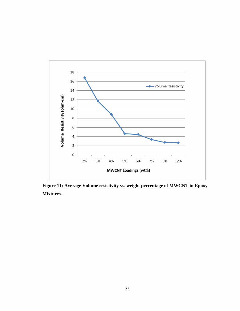
23
Figure 11: Average Volume resistivity vs. weight percentage of MWCNT in Epoxy
Mixtures.
0
2
4
6
8
10
12
14
16
18
2% 3% 4% 5% 6% 7% 8% 12%
Volume Resistivity
MWCNT Loadings (wt%)
Vol
ume
Res
isti
vity
(ohm
-cm
)

24
Figure 12: Average volume resistivity vs. weight percentage of SMWCNTs in Epoxy
mixture.
0
5
10
15
20
25
30
35
40
15% 18% 20%
stddeviation
resistivity
Vol
ume
Resi
stiv
ity ρ(Ω
-cm
)
SMCWNT loading(wt%)

25
5.1.3 MWCNT Loadings with Epoxy/Heloxy composite vs. Volume Resistivity
The volume resistivity was also measured by varying Epoxy-Heloxy composition.
The heloxy is a viscosity modifier which when added decreases the viscosity of the
composite. We then varied the weight proposition of the epoxy heloxy from 40:60, 50:50,
and 60:40 for 14% loadings of MWCNTs. The 70:30 and 30:70 was limited to 12%
MWCNTs. The variation of the resistivity for different weight percentages and the
proportion of Epoxy-Heloxy composition are plotted as shown in the Figure 14. The 1:1
composition demonstrates a decreasing resistivity with increasing MWCNT loading,
while the 2:3 and 3:2 ratios show minimum resistivities at 12 wt%.
Figure 13: Average volume resistivity versus Epoxy to Heloxy ratio and weight percentage of MWCNT in Epoxy-Heloxy mixtures.
0
0.5
1
1.5
2
2.5
3
8% 12% 8% 12% 14% 8% 12% 14% 8% 12% 14% 8% 12%
3:07 2:3 1:1 3:2 7:03
std deviation
ρ(Ω-cm)
Vol
ume
Res
isti
vity
(ohm
-cm
)
Epoxy : Heloxy

26
5.2 Contact Resistance Results and Discussion
5.2.1 Contact resistance results for MWCNT epoxy composite
Contact resistance measurement tests were conducted with 50um long MWCNT.
The following table shows the experimental results for contact resistance measurements
for various loadings on three different metals likely tin, gold and silver. This set of results
is taken immediately after curing the sample. The results obtained from the experiments
are shown in Table 2.
Although the contact resistance daisy chains allow us to average 80 contact points
per test board, the results are often dominated by a few high resistance joints. The
resulting data includes large standard deviations from various sample combinations. All
three surface finishes silver, tin and gold displayed the extreme variance leading us to
focus on tin coated boards as the least expensive test circuits. Unlike the volume
resistivity graphs, the data presented in Figure 15 for average contact resistance does not
show a clear trend as a function of loading wt%.
One explanation for the variability in the contact resistance data may be the absence of
flux. Lead-tin and lead free solders contain thermally activated flux compounds to
remove native oxides from the circuit board pads and component leads at temperatures
below the melting point of the solder. The MWCNT filled adhesives do not contain a
fluxing agent and rely primarily on pressure applied during curing to form electrical
contacts between the component leads, nanotubes and circuit board pads. Conversely,
MWCNT filled adhesives do not produce flux residues and therefore eliminate the need
for cleaning and reduce long term corrosion of printed circuit assemblies.
It is observed that applying pressure on zero ohm resistors during curing
dramatically improves conductivity. It is also observed that the contact resistance is
variable with % loading and surface finishes. All the values are high for use as a solder
replacement. In general, the obtained values from figure 15 indicate that contact
resistance for gold is highest and for silver is least in the order Rag > Rsn > RAu.
A shift in contact resistance is also observed for each of these samples after room
temperature storage illustrating that contact resistance increases with aging time. This
may be because of galvanic corrosion of metal after moisture penetrated into cured

27
polymer matrix and condensed at the interface between ECA and metal surface. Galvanic
corrosion happens only under wet conditions with the presence of an electrolyte solution.
Moisture absorbed by the cured ECA diffuses into the interface between the ECA and the
non noble metal and forms an electrolyte solution. Metal oxide formation caused by
galvanic corrosion of the non noble metal at the interface is responsible for the contact
resistance increase.
Table 2: Contact resistance on different surface finished PCBs for different
MWCNT (wt%)-Epoxy composite.
Loading (wt %)
Silver tin gold Average
resistance Std
Deviation Average
resistance Std
Deviation Average
resistance Std
Deviation
2% 127.5 73.6 239.625 73.5 X X
3% 361.125 77.9 387.5 381.5 906.667 100.5
4% 216 102.9 665 325.1 550 317.4
5% 258.25 137.1 478.75 192.6 488.75 99.53
6% 211.25 88.4 353.75 36.1 812.5 238.5

28
5.2.2 Contact resistance results for MWCNT epoxy: heloxy composite:
The contact resistance values for the epoxy composite were svery high so we tried
additional formulations using the heloxy, viscosity modifier. The combinations were
30:70, 40:60, 50:50, 60:40, and 70:30, as before. The MWCNT loadings that we tested
were 8%, 12% and 14%. All the loadings were tested on three different PCB surface
finishes silver, tin and gold. The values are represented in the following graphs. There are
a many values so for better understanding the data were grouped by MWCNT loading..
The graphs are shown in Figure 15, Figure 16 and Figure 17 for 8, 12 and 14%
respectively.
From the above figures, it is clear that by adding Heloxy to the composition, the
contact resistance values are reduced by 1/10 of the previously observed results obtained
with epoxy-MWCNT composition. As Heloxy acts as viscosity modifier of Resin, the %
loading of the MWCNTs in the mixture is able to be increased. Previously, the % loading
is limited to 12% with only epoxy, but by adding Heloxy, the loading limit is increased to
14 wt%. Above the loading limit, the MWCNTs do not disperse well and the adhesive is
not processable by screen printing. It is observed that of all metals, tin has shown least
contact resistance with E-H composition. The minimum contact resistance with least
variability for all the metals for 8% loading is observed at 2:3 ratio of epoxy-Heloxy, for
12% loading at 3:2 Composition and for 14% at 3:2.
It can also be observed that silver has shown least contact resistance of all the
three metals. Gold has the highest value. Tin has shown consistent values at 12 wt%
loading. This type of behavior from gold is seen at 14 wt% loading. Silver has shown
decreasing contact resistance with increase in Heloxy ratio for 14 wt%. Though the
obtained values are not consistent enough for applications, these variations in the values
may be due to outlier contacts in the chain. This presence of faulty resistance may
increase the average value of the chain, thus increasing the resistance per contact on the
whole. The variations in resistance for same batch of mixture for all the three metals may
be because of the pot life of the mixture and its process ability after it is stored.

29
Figure 14: Average Contact resistance on different surface finished PCBs with
8wt% MWCNT loading and varying epoxy-Heloxy ratios.
0
200
400
600
800
1000
1200
1400
1600
Tin Silver Gold Tin Silver Gold Tin Silver Gold Tin Silver Gold Tin Silver Gold
3–7 2–3 1–1 3–2 7–3
30 40 50 60 70
cont
act r
esis
tanc
e in
ohm
s
Epoxy----------------------------------------------------------------------------------------------------> <----------------------------------------------------------------------------------------------------Heloxy
8% MWCNT loading
Standard deviation
Contact Resistance(Ω)

30
Figure 15: Average Contact resistance on different surface finished PCBs with
12wt% MWCNT loading and varying epoxy-Heloxy ratios.
0
100
200
300
400
500
600
700
800
900
Sn Ag Au Sn Ag Au Sn Ag Au Sn Ag Au Sn Ag Au
3–7 2–3 1–1 3–2 7–3
cont
act r
esis
tanc
e in
ohm
s
Epoxy------------------------------------------------------------------------------------------------><--------------------------------------------------------------------------------------------Heloxy
12% MWCNT
Standard deviation
Contact Resistance(Ω)

31
Figure 16: Average Contact resistance on different surface finished PCBs with
14wt% MWCNT loading and varying Epoxy-Heloxy ratios.
0
200
400
600
800
1000
1200
Sn Ag Au Sn Ag Au Sn Ag Au
2–3 1–1 3–2
Epoxy----------------------------------------------------------------------------------------><------------------------------------------------------------------------------------------Heloxy
14% MWCNT
Standard deviation
Contact Resistance(Ω)
cont
act r
esis
tanc
ein
ohm
s

32
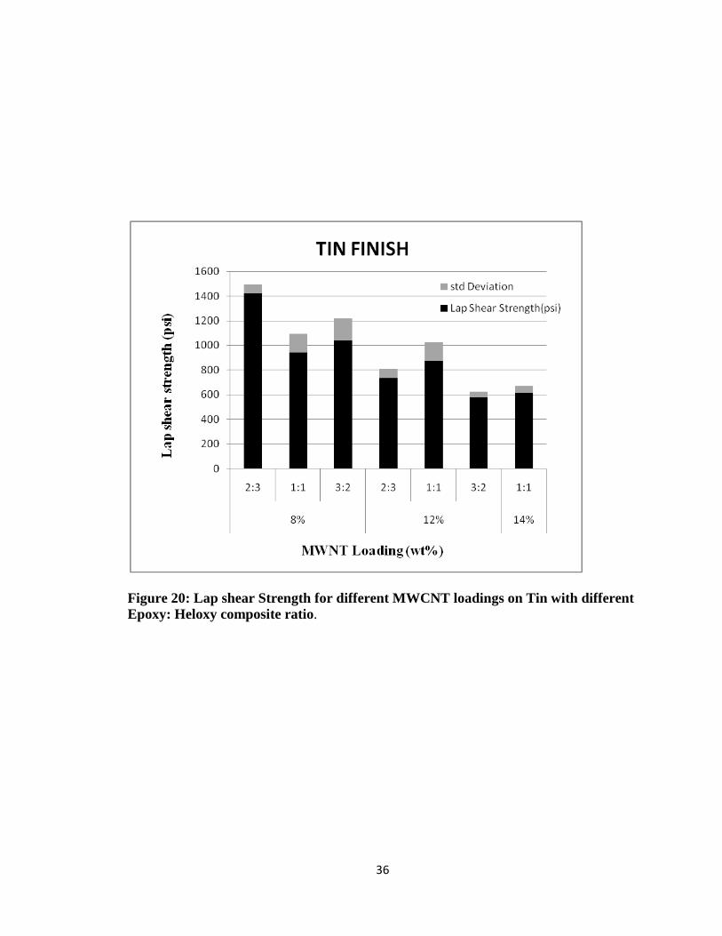
5.3 Lap shear Results and Discussions:
The lap shear strength for the samples was tested on silver, tin and gold for the
loadings of 2%, 3%, 4% and 8% with the epoxy composite. The strength was measured in
pound per square inch (psi). The lap shear strength was observed to be very high when
compared to the Ag filled adhesive which is of the order of 200 psi. The values obtained
for different metals for different loadings are presented in a graphical plot as shown in
Figure 18.
From the graph we can observe that the lap shear strength for gold is higher the
silver and tin finishes. The trend shows that the lap shear strength decreases with the
increase in the loading of MWCNTs. The lap shear strength is way higher when
compared to the Ag filled adhesive.
The next step was the addition of the heloxy, a viscosity modifier to the epoxy
composite to help improve the electrical properties. Different epoxy and heloxy
combinations were used like 2:3, 1:1, and 3:2. The loadings that were tested on the
composite were 8%, 12%, 14%. The tests were conducted on the tin, silver and gold
metals. The figures 19, figure 20 and figure 21 show the results of the strengths of all the
three metals individually.
From the results obtained we observe that the lap shear strength is high at lower
MWCNT loadings and decreases with the increase in the loadings. The best values
obtained are at 8% loadings for gold at 2:3 composite ratio, for silver at 1:1 composite
ratio and tin at 2:3 composite ratio.

33
Figure 17: Lap shear Strength for different MWCNT loadings on Gold, Silver and
Tin with Epoxy composite.
0
500
1000
1500
2000
2500
3000
silver gold tin silver gold tin silver gold tin silver gold tin
2% 3% 4% 8%
std deviation
lap shear strength(psi)
lap
she
ar s
tren
gth
(psi
)
MWCNT loading (wt %)

34
Figure 18: Lap shear Strength for different MWCNT loadings on Gold with
different Epoxy: Heloxy composite ratio.

35
Figure 19: Lap shear Strength for different MWCNT loadings on Silver with different Epoxy: Heloxy composite ratio.
36
Figure 20: Lap shear Strength for different MWCNT loadings on Tin with different Epoxy: Heloxy composite ratio.

37
5.4 Die Shear Results and Discussion:
The experiment that was conducted on a test board which had 32 pads
each of a different surface finish. The MWCNT/epoxy was dispensed on to the pads by
an air pressure dispenser. A manual pick and place a place machine was used to attach
the dies on to the pads. The size of the die is 0.06 inch ×0.05 inch = 0.003 inch2
The Figure 22 shows the shear strength values obtained for different surface
finishes at different MWCNT loadings. It was observed that the values obtained are
higher than the minimum requirement. Compared to all the three surface finishes silver
has the high die shear strength for all the loadings. The high standard deviation shows
there is a large variance in the die shear strength. It may be due to the variance in the
amount of composite being dispensed and the adhesion of the die on to the pad.
.
According to the Mil-Std-883 Method 2019, the minimum strength for this die is 2.5Kg.
5.5 Aging Experiments Results and Discussion:
The aging experiments were done all the 12% MWCNT/ Epoxy: Heloxy
composite samples. The results indicate that the volume resistivity of the samples
increased and decreased for different ratios of Epoxy: Heloxy. It is show in Figure 23
below. We observe for 7:3 there is very slight variation in the values.

38
Figure 21: Die shear Strength for different MWCNT loadings on Gold, Silver, and
Tin with Epoxy composite.
0
5
10
15
20
25
silver tin gold silver tin gold silver tin gold silver tin gold silver tin gold
2% 3% 4% 5% 6%
Std Deviation
Shear Strength (KG)
MWCNT Loading (wt%)
Die
She
ar S
tren
gth
(Kg)

39
Figure 22: Variation of volume resistivity with aging experiments on 12% MWCNT/
Epoxy: heloxy composite.
0
0.2
0.4
0.6
0.8
1
1.2
3:7 2:3 1:1 3:2 7:3
before
24hrs at 85c
72hrs at 85c
Vol
ume
Res
istiv
ity (o
hm-c
m)
Epoxy : Heloxy Composite ratio
12% MWCNT Loading
40
Chapter6 Conclusion and Future Work
The research focuses on the potential of replacing metal fillers with MWCNTs in
electrically conductive adhesives with good electrical and mechanical properties and
testing the conductive adhesives on different surface finishes like gold, silver and tin.
Electrical conduction and mechanical strength of the MWCNT/epoxy composite and the
MWCNT/epoxy: heloxy composite were analyzed.
The results for the epoxy/MWCNT composite shows that the volume resistivity
decreases with the increase in the loading. Above 12% loading the epoxy composite is
not processable. The volume resistivity for the epoxy:heloxy/MWCNT composite was
reduced even more when compared to the epoxy/MWCNT composite. SMWCNT/epoxy
composite gave very high values, although higher loadings up to 20% were possible.
Contact resistance values were very high for the epoxy/MWCNT composite. The contact
resistance reduced by 10 times for the epoxy:heloxy/MWCNT composite when compared
to the epoxy/MWCNT. However, the volume resistivity and contact resistance are not
comparable to the commercially available metal filled ICAs.
The results for lap shear strength with epoxy/MWCNT on different metals was
high when compared to the metal filled ICAs. The lap shear strength decreased with the
usage of heloxy in the composite but was still higher than the metal filled ICAs. The
results for the die shear strength for the epoxy/MWCNT composite were higher than the
standards. The MWCNT filled adhesive has good mechanical properties than the metal
filled ICAs.
The preparation of the composite involved the usage of epoxy, curing agent,
heloxy and catalyst. The pot life for the composite was observed to be 72 hrs. The
composite was able to be reused when refrigerated. The MWCNT filled adhesives were
compatible with oven curing, pressure dispensing and stencil printing.

41
Based on the results from the thesis, the possible directions to extend this research can be
as follows:
The rework of the conductive adhesives which is analogous to desoldering of
solder paste.
A detailed study of chemical reactions involved between the surface finishes and
epoxy mixtures used.
Investigate the properties of the composite by mixing the MWCNTs with Ag
flakes and carrying out electrical and mechanical properties.
Even though gold does not form oxides we obtained a large value of contact
resistances. This can be due to Ni coating on copper pads before gold is coated. A
deeper study into the chemical reactions is needed.
A good detailed study of the accelerated aging tests using the environmental
chamber is a good topic.

42
REFERENCES [1] J. Liu, K. Gustafsson, Z. Lai and C. Li, “Surface Characteristics, Reliability, and Failure Mechanisms of Tin/Lead, Copper, and Gold Metallizations”, IEEE Transactions on Components, Packaging, and Manufacturing Technology, Part A, 20, 21-30, 1997. [2] D. Lu and C. P. Wong, “Development of Conductive Adhesives Filler with Low-melting point Alloy Fillers”, International Symposium on Advanced Packaging Materials, Port Erin, Isle of Man, British Isles, 7-13, 2000. [3] S. Xu and D. A. Dillard, “Environmental Aging Effects on Thermal and Mechanical Properties of Electrically Conductive Adhesives”, The Journal of adhesion ISSN 0021-8464 vol. 79, no
7, pp. 699-723, 2000.
[4] S. Xu and D. A. Dillard, Environmental Aging Effects on the Durability of Conductive Adhesive Joints, International Journal of Adhesion and Adhesives ,Volume 23, Issue 3, 2003, Pages 235-250. [5] M. Zwolinski, J. Hickman, H. Rubin, Y. Zaks, S. McCarthy, T. Hanlon, P. Arrowsmith,A. Chaudhuri, R. Hermansen, S. Lau, and D. Napp, “Electrically Conductive Adhesives for Surface Mount Solder Replacement,” IEEE Transactions on Components, Packaigng,and Manufacturing Technology, Part C, 19, 241-250. 1996. [6] Daniel F. Baldwin, Fundamentals of Microsystems Packaging, edited by Rao R. Tummala, McGraw Hill, New York, 2001.
[7] L. Ying, A reworkable high reliability thermoplastic die attach adhesive, Proceedings international symposium on microelectronics (1986) 621-631
[8] K. Harry, Organic solder - a new type of adhesive/conductor for electronics, 1st International SAMPE electronics conference - Electronic materials and processes, (1987) 168-179
[9] Daoqiang Daniel lu and C.P.Wong, Recent Advances in developing Performance Isotropic Conductive Adhesives, Journal of Adhesion science and technology 22(2008)835-851.
[10] Yi Li, C.P. Wong, Recent advances of conductive adhesives as a lead-free alternative in electronic packaging: Materials processing, reliability and applications, Materials Science and Engineering: R: Reports, Volume 51, Issues 1-3, 30 January 2006,
Pages 1-35.
[11] John H. Lau, C. P. Wong, Ning Cheng Lee, S. W. Ricky Lee, Electronics Manufacturing with Lead-free, Halogen-free & Conductive Adhesive Materials, McGraw Hill, New York, 2003.
[12] Shuangyan Xu, Evaluating Thermal and Mechanical Properties of Electrically
43
Conductive Adhesives for Electronic Applications, Dissertation submitted to the faculty of the Virginia Polytechnic Institute and State University, April, 2001, Blacksburg, Virginia. [13] Krätschmer, W. (1990). "Solid C60: a new form of carbon". Nature 347: 354 - 358.
[14] http://physicsworld.com/cws/article/print/1761.
[15] Andreas Thess, Roland Lee, Pavel Nikolaev, Hongjie Dai, Pierre Petit, Jerome Robert, Chunhui Xu, Young Hee Lee, Seong Gon Kim, Andrew G. Rinzler, Daniel T. Colbert, Gustavo Scuseria, David Tománek, John E. Fischer, Richard E. Smalley, "Crystalline Ropes of Metallic Carbon Nanotubes", Science 273, 483 (1996). [16] Savas Berber, Young-Kyun Kwon, and David Tomànek, "Unusually High Thermal Conductivity of Carbon Nanotubes", Phys. Rev. Lett. 84 (2000). [17] Min-Feng Yu, Bradley S. Files, Sivaram Arepalli, and Rodney S. Ruoff, "Tensile Loading of Ropes of Single Wall Carbon Nanotubes and their Mechanical Properties", Phys.Rev. Lett. 84 (2000). [18] Guanghua Gao, Tahir Cagin, and William A. Goddard III, "Energetics, Structure, Mechanical and Vibrational Properties of Single Walled Carbon Nanotubes (SWNT)", Nanotechnology 9 184-191 (1998).
[19] Jon O'Connell, “Study and recommendations into using lead free printed circuit board finishes at manufacturing in circuit test stage”, Agilent Technologies UK Ltd, Automated Test group. [20] J.Li, J.K. Lumpp, R. Andrews, D. Jacques, “Aspect Ratio and Loading Effects of Multiwall Carbon Nanotubes in Epoxy for Electrically Conductive Adhesives”, Journal of Adhesion Science and Technology, Volume 22, Number 14, 2008 , pp. 1659-1671(13). [21] Die shear strength MIL-STD-883E NOTICE 5 Method 2019.7, 07 March 2003. [22] Keerthivarma Mantena, Jing Li, Lumpp, Janet K., “Electrically Conductive Carbon Nanotube Adhesives on Lead Free Printed Circuit Board surface Finishes”, Proc. IEEE Aerospace Conference, Big Sky, MT, March 2008 [23] Keerthivarma Mantena, Dr. Janet K. Lumpp, Naveen Velicheti, Midhun Jasti, Poojitha Sirigiri, “Electrical and Mechanical Properties of Carbon Nanotube Filled Adhesives on Lead Free PCB Surface Finishes”, Proc. International Microelectronics and Packaging Symposium,Providence, RI, October 2008

44
VITA
Keerthivarma Mantena was born on October 4, 1983 in Hyderabad, Andhra Pradesh, India. He received the Bachelors of Engineering degree in Electrical and Electronics Engineering from Anna University, Chennai, Tamilnadu , India, in 2005. His research is extending the carbon nanotube filled conductive adhesive work to evaluate lead free surface finishes. In 2006 he began to study in department of Electrical Engineering at University of Kentucky. Publications:
• Keerthivarma Mantena, Jing Li, Lumpp, Janet K., “Electrically Conductive Carbon Nanotube Adhesives on Lead Free Printed Circuit Board surface Finishes”, Proc. IEEE Aerospace Conference, Big Sky, MT, March 2008.
• Keerthivarma Mantena, Dr. Janet K. Lumpp, Naveen Velicheti, Midhun Jasti, Poojitha Sirigiri, “Electrical and Mechanical Properties of Carbon Nanotube Filled Adhesives on Lead Free PCB Surface Finishes”, Proc. International Microelectronics and Packaging Symposium,Providence, RI, October 2008.