
Electric field drives the nonlinear resonance of a piezoelectric nanowire
6
Solid State Communications 144 (2007) 118–123 www.elsevier.com/locate/ssc Electric field drives the nonlinear resonance of a piezoelectric nanowire Jun Zhou a , Zhonglin Wang a , Anton Grots b , Xiaoling He b,* a School of Materials Science and Engineering, Georgia Institute of Technology, Atlanta, GA 30332-0245, USA b Mechanical Engineering, University of Wisconsin, Milwaukee, WI 53211, USA Received 1 May 2007; accepted 10 August 2007 by E.G. Wang Available online 22 August 2007 Abstract This paper studies the nonlinear vibration of a ZnO nanowire driven by an external electric field. The equation of motion for the nanowire with a nonlinear elastic deformation is formulated. The numerical computation results reveal the nonlinear vibration behaviors of the nanowire subject to the applied electric field with the piezoelectric field effect. The results agree with the experimental observations in the nanowire deflection behaviors. It is demonstrated that the nanowire is in a finite periodic oscillation subject to the applied field strength, with bifurcations leading to resonance recurrence. Published by Elsevier Ltd PACS: 05.45.–a; 85.35.–p; 81.07.–b; 85.85.+j; 77.84.–s Keywords: A. Nanostructures; C. Piezoelectricity; D. Elasticity 1. Introduction Piezoelectric nanowires and nanobelts have shown promise as sensors and actuators for manipulation, detection, scanning and motion control at nano- to micro-scales [1–4]. ZnO nanobelts and nanowires are the most typical quasi-one- dimensional structures used for these applications as gas sensors, semiconducting Schottky diodes and piezoelectric generators, among others [5,6]. The non-toxic property of ZnO also makes the nanowire a good candidate for implantable devices in biomedical applications. The functionality of a piezoelectric device is largely based on its resonance characteristics, similar to micro-electro-mechanical system (MEMS) devices. Therefore, predictable mechanical behavior of the nanostructures is key to ensure their controlled functionality for reliable applications. Different forms of ZnO morphologies in a single-crystal structure have been synthesized by physical and chemical vapor deposition, including nanodisks, nanowires and nanobelts etc. [3,7]. Experimental studies have demonstrated that a ZnO nanowire presents elastic deformations subject to an alternating current (AC) or a direct current (DC) electric field. The large * Corresponding author. Fax: +1 414 229 6958. E-mail address: [email protected] (X. He). degree of nanowire deformation falls into the nonlinear regime, since the deflection is larger than the critical dimension in terms of the nanowire radius in a hexagonal cross-section [8–10]. In addition, the deformation of the ZnO nanowire invokes the piezoelectric effect due to the disposition of the electrons along with the deflection of the nanowire [11]. This effectively makes the nanowire a nanogenerator energized by the mechanical deformation or vibration. Note that the nonlinear mechanical vibration of the nanowire can also be invoked by the acoustic waves, or by other forms of the driving force other than the electric field [12] that causes the mechanical deflection of the nanowire. The ZnO nanowire that demonstrated the nonlinear deformation with the piezoelectric effect, as demonstrated in the experiments [10], was synthesized by a vapor–solid growth process. The AC and DC fields applied an electric potential of V AC = 10 V and V DC = 28 V to the nanowire, which caused the ZnO nanowire to vibrate. Fig. 1(a) and (b) show the frequency responses of a nanowire cantilever with a length L = 109 μm and a diameter a = 305 nm. It is evident that the deformation is nonlinear since the deflection is about 2–14 μm, which is much larger than the diameter a = 305 nm. Driven by the applied electric field, the piezoelectric effect generates a potential along the axis due to the polarized surfaces at the top and the bottom of the hexagonal surfaces [13]. 0038-1098/$ - see front matter Published by Elsevier Ltd doi:10.1016/j.ssc.2007.08.011
Transcript of Electric field drives the nonlinear resonance of a piezoelectric nanowire

Solid State Communications 144 (2007) 118–123www.elsevier.com/locate/ssc
Electric field drives the nonlinear resonance of a piezoelectric nanowire
Jun Zhoua, Zhonglin Wanga, Anton Grotsb, Xiaoling Heb,∗
a School of Materials Science and Engineering, Georgia Institute of Technology, Atlanta, GA 30332-0245, USAb Mechanical Engineering, University of Wisconsin, Milwaukee, WI 53211, USA
Received 1 May 2007; accepted 10 August 2007 by E.G. WangAvailable online 22 August 2007
Abstract
This paper studies the nonlinear vibration of a ZnO nanowire driven by an external electric field. The equation of motion for the nanowire witha nonlinear elastic deformation is formulated. The numerical computation results reveal the nonlinear vibration behaviors of the nanowire subjectto the applied electric field with the piezoelectric field effect. The results agree with the experimental observations in the nanowire deflectionbehaviors. It is demonstrated that the nanowire is in a finite periodic oscillation subject to the applied field strength, with bifurcations leading toresonance recurrence.Published by Elsevier Ltd
PACS: 05.45.–a; 85.35.–p; 81.07.–b; 85.85.+j; 77.84.–s
Keywords: A. Nanostructures; C. Piezoelectricity; D. Elasticity
1. Introduction
Piezoelectric nanowires and nanobelts have shown promiseas sensors and actuators for manipulation, detection, scanningand motion control at nano- to micro-scales [1–4]. ZnOnanobelts and nanowires are the most typical quasi-one-dimensional structures used for these applications as gassensors, semiconducting Schottky diodes and piezoelectricgenerators, among others [5,6]. The non-toxic property of ZnOalso makes the nanowire a good candidate for implantabledevices in biomedical applications. The functionality ofa piezoelectric device is largely based on its resonancecharacteristics, similar to micro-electro-mechanical system(MEMS) devices. Therefore, predictable mechanical behaviorof the nanostructures is key to ensure their controlledfunctionality for reliable applications.
Different forms of ZnO morphologies in a single-crystalstructure have been synthesized by physical and chemicalvapor deposition, including nanodisks, nanowires and nanobeltsetc. [3,7]. Experimental studies have demonstrated that a ZnOnanowire presents elastic deformations subject to an alternatingcurrent (AC) or a direct current (DC) electric field. The large
∗ Corresponding author. Fax: +1 414 229 6958.E-mail address: [email protected] (X. He).
0038-1098/$ - see front matter Published by Elsevier Ltddoi:10.1016/j.ssc.2007.08.011
degree of nanowire deformation falls into the nonlinear regime,since the deflection is larger than the critical dimension in termsof the nanowire radius in a hexagonal cross-section [8–10].In addition, the deformation of the ZnO nanowire invokes thepiezoelectric effect due to the disposition of the electrons alongwith the deflection of the nanowire [11]. This effectively makesthe nanowire a nanogenerator energized by the mechanicaldeformation or vibration. Note that the nonlinear mechanicalvibration of the nanowire can also be invoked by the acousticwaves, or by other forms of the driving force other than theelectric field [12] that causes the mechanical deflection of thenanowire.
The ZnO nanowire that demonstrated the nonlineardeformation with the piezoelectric effect, as demonstrated inthe experiments [10], was synthesized by a vapor–solid growthprocess. The AC and DC fields applied an electric potential ofVAC = 10 V and VDC = 28 V to the nanowire, which caused theZnO nanowire to vibrate. Fig. 1(a) and (b) show the frequencyresponses of a nanowire cantilever with a length L = 109 µmand a diameter a = 305 nm. It is evident that the deformation isnonlinear since the deflection is about 2–14 µm, which is muchlarger than the diameter a = 305 nm. Driven by the appliedelectric field, the piezoelectric effect generates a potential alongthe axis due to the polarized surfaces at the top and the bottomof the hexagonal surfaces [13].

J. Zhou et al. / Solid State Communications 144 (2007) 118–123 119
(a) The first resonance.
(b) Frequency response and resonance.
(c) Experimental setup.
Fig. 1. Experimental frequency response.
The ZnO nanowire in a single-crystal Wurzite structure withan atomic radius of a = 3.25 A, c = 5.205 A generallygrows to a cross-sectional dimension in the micrometer range,e.g., a = 305 nm. For a micro-sized beam of ZnO of sucha dimension, it contains an accumulated single crystal ofZnO of about 1000 × 625 units in the cross-section. Treatingthe closely packed discrete crystal structure as a continuumeffectively links the dynamics of the ZnO nanowires to themicrobeam dynamics. In addition, the nanowire beam can beviewed as being quasi-isotropic. This is because there is a minordifference between the vertical and the horizontal directions ofthe cross section in their elastic properties. Studies confirmedthat the Young’s modulus of the vertical and the horizontaldirection of the cross-section are almost identical, i.e., about8% different [8]. Such a quasi-isotropic property in the cross-section gives rise a homogeneous hexagonal beam for the singlemode deflection. This justifies reducing a two-dimensionalelastic plate theory to the one-dimensional beam theory, or aplate-strip theory, to describe the nanowire dynamics. Despitethe similarities of the nanowire to a microbeam, the single-crystalline structure and the piezoelectric field effect distinguishthe nanowire from an elastic microbeam in the following twoaspects: on the one hand, the discrete atomic structure requiresconsiderations of energy balance when applying the continuumelastic theory to study the single-crystal structure vibration. On
the other hand, the piezo-electric effect produces electric fieldgradients along the beam axis and transverse to the axis, whichtranslates into in-plane forces and the bending moment actingon the beam.
Prior studies on the nonlinear vibration of the microbeamor the plate-strip have been based largely on the von Karmanstrain field in nonlinear plate theory by reducing the plate toa one-dimensional belt. In this approach, Younis and Nayfehinvestigated an isotropic microbeam behavior subject to theelectrostatic force generated by the AC and DC electricfields [14]. Their reduction of the governing equation of motionby using the Galerkin method led to the Duffing equation for themicrobeam vibration in the single mode response. Resonancewas characterized by the perturbation method in multiplescales. Pamidighantam et al. studied the nonlinear effect on theelectro-statically actuated microbeam structure with differentboundary conditions [15]. Their study focused on the effectivenonlinear spring stiffness influenced by the electric chargeredistribution, the boundary condition and the electric fieldfringing effect associated with the capacitor model that theyadopted. The results refined the prior studies in determiningthe pull-in voltage of the MEMS devices. In a separate study,Awrejcewicz et al. studied the bifurcation behaviors of theplate strip by examining the stabilities due to variations inthe load [16,17]. A closely related work by Li et al. on themicrobeam nonlinear dynamics concerns the probe response ofthe atomic force microscopy that exhibits bifurcations arisingfrom either the intermittent forcing or a nonlinear forcingfunction, rather than from the large deflection of a beam [18].
Although the experimental observations reveal the nano-wire’s large deformation, little is known about the nanowire’snonlinear dynamics behavior to explain the experimentalobservations of the recurrence of resonance and to describethe oscillation characteristics that is potentially associated withbifurcations and chaos. In this paper, we develop a nonlinearelastic model for the nanowire dynamics in a clamped-freeboundary condition subject to an AC or DC electric field.To this end, we apply the von Karman plate theory andthe Galerkin method to obtain the equation of motion. TheDuffing equation obtained from such a reduction incorporatesthe elastic properties of the single-crystal structure nanowire forthe fundamental mode response. In addition, the polarizationeffect of the nanowire is considered by relating the deformationto the piezoelectric field potential. To characterize the responseof the nanowire subject to the electric field, the fourth-order Runge–Kutta method is employed in the numericalcomputation to demonstrate the frequency response and thetransient response in Poincare maps. Our purpose is to developa model to characterize the experimental response. Therefore,we compare the computation results and the experimentalobservations to validate our model.
2. Theoretical modeling
2.1. Nanowire subject to an electric field
The nanowire under investigation is in a clamped-freeboundary condition subject to AC and DC electric fields, as de-scribed in the experimental setup in [10]. Fig. 1(c) illustrates
120 J. Zhou et al. / Solid State Communications 144 (2007) 118–123
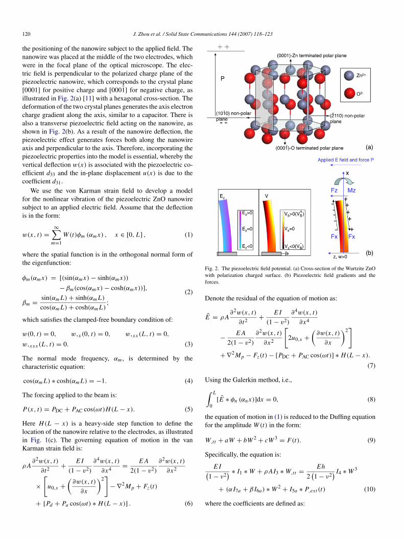
the positioning of the nanowire subject to the applied field. Thenanowire was placed at the middle of the two electrodes, whichwere in the focal plane of the optical microscope. The elec-tric field is perpendicular to the polarized charge plane of thepiezoelectric nanowire, which corresponds to the crystal plane[0001] for positive charge and [0001] for negative charge, asillustrated in Fig. 2(a) [11] with a hexagonal cross-section. Thedeformation of the two crystal planes generates the axis electroncharge gradient along the axis, similar to a capacitor. There isalso a transverse piezoelectric field acting on the nanowire, asshown in Fig. 2(b). As a result of the nanowire deflection, thepiezoelectric effect generates forces both along the nanowireaxis and perpendicular to the axis. Therefore, incorporating thepiezoelectric properties into the model is essential, whereby thevertical deflection w(x) is associated with the piezoelectric co-efficient d33 and the in-plane displacement u(x) is due to thecoefficient d31.
We use the von Karman strain field to develop a modelfor the nonlinear vibration of the piezoelectric ZnO nanowiresubject to an applied electric field. Assume that the deflectionis in the form:
w(x, t) =
∞∑m=1
W (t)φm (αm x) , x ∈ [0, L] , (1)
where the spatial function is in the orthogonal normal form ofthe eigenfunction:
φm(αm x) = [(sin(αm x) − sinh(αm x))
− βm(cos(αm x) − cosh(αm x))],
βm =sin(αm L) + sinh(αm L)
cos(αm L) + cosh(αm L);
(2)
which satisfies the clamped-free boundary condition of:
w(0, t) = 0, w,x (0, t) = 0, w,xx (L , t) = 0,
w,xxx (L , t) = 0. (3)
The normal mode frequency, αm , is determined by thecharacteristic equation:
cos(αm L) ∗ cosh(αm L) = −1. (4)
The forcing applied to the beam is:
P(x, t) = PDC + PAC cos(ωt)H(L − x). (5)
Here H(L − x) is a heavy-side step function to define thelocation of the nanowire relative to the electrodes, as illustratedin Fig. 1(c). The governing equation of motion in the vanKarman strain field is:
ρ A∂2w(x, t)
∂t2 +E I
(1 − v2)
∂4w(x, t)∂x4 =
E A2(1 − v2)
∂2w(x, t)∂x2
×
[u0,x +
(∂w(x, t)
∂x
)2]
− ∇2 Mp + Fz(t)
+ [Pd + Pa cos(ωt) ∗ H(L − x)] . (6)
Fig. 2. The piezoelectric field potential. (a) Cross-section of the Wurtzite ZnOwith polarization charged surface. (b) Piezoelectric field gradients and theforces.
Denote the residual of the equation of motion as:
E = ρ A∂2w(x, t)
∂t2 +E I
(1 − v2)
∂4w(x, t)∂x4
−E A
2(1 − v2)
∂2w(x, t)∂x2
[2u0,x +
(∂w(x, t)
∂x
)2]
+ ∇2 Mp − Fz(t) − [PDC + PAC cos(ωt)] ∗ H(L − x).
(7)
Using the Galerkin method, i.e.,∫ L
0[E ∗ φn (αn x)]dx = 0, (8)
the equation of motion in (1) is reduced to the Duffing equationfor the amplitude W (t) in the form:
W,t t + aW + bW 2+ cW 3
= F(t). (9)
Specifically, the equation is:
E I(1 − ν2
) ∗ I1 ∗ W + ρ AI3 ∗ W,t t =Eh
2(1 − ν2
) I4 ∗ W 3
+ (α I7a + β I6a) ∗ W 2+ I5a ∗ P ext (t) (10)
where the coefficients are defined as:

J. Zhou et al. / Solid State Communications 144 (2007) 118–123 121
I1 = φ,xxxx ∗ φ; I2 =(φ,xx ∗ φ
);
I3 = φ ∗ φ; I4 =
(φ2
,x
)∗
(φ,xxφ
);
I5a = φ ,x φ; I6a = φ2,xφ;
I7a =
(φ,2
xx φ + φ,x φ,xxx φ)
.
(11)
2.2. The piezoelectric effect
The coefficients α and β are associated with the piezoelectricforces. Using a parallel capacitor model [19], the deflectionw(x), the piezoelectric potential Vmax and the piezoelectricconstant d33 have a relation as follows:
Vmax =T2d
θmax, V =T θ
2d=
T2d
w,x =T2d
w,x . (12)
For convenience, we used d instead of d33 in the above and theensuing formulations. Note that the effect of d31 is negligibledue to the applied field that is transverse to the nanowireaxis, which generates a negligible electric charge due to d31.The surface charge density is mainly due to the transverseelectric field Ez . The electric field gradients Ez and Ex can bedetermined as:
Ez =VT
=1
2dw,x , Ex =
VL
=
√3a
2d Lw,x . (13)
Referring to [13], the piezoelectric field gradient has a positivecharge on the stretched surface and a negative charge on thecompressed surface. In addition, the field gradient increasesfrom the clamped end to the free end due to a larger deflectionalong the polarization axis. This generates an axial force Fxalong the two charged surfaces and a transverse force Fz , asillustrated in Fig. 2(b). The increasing gradient along the axisdefines that the axial force produces a moment that opposes thedeflection caused by the external electric field. This force ofunit length is given by:
fx =12σ Ex =
12
Ez Exε =εa1
4Ld2 θ2=
√3εa
8Ld2 w2,x . (14)
The accumulated in-plane force Nx is:
Nx = fx ∗ aL =
√3εa2
8d2 w2,x . (15)
Nx produces a bending moment as:
M = −Nx ∗ 2a1 = −
√3εa3
8d2 w2,x = −αw2
,x ,
α =εa2
1a4d2 =
3εa3
8d2 , a1 =
√3
2a. (16)
A transverse force is generated by the transverse electricgradient Ez , which is in the same direction as the applied field.The transverse force is:
Fz =12σ Ez ∗ a =
12
aε(α
d
)2=
aε
8
(θ
d
)2
=aε
8d2 w2,x = βw2
,x ; β =aε
8d2 . (17)
The transverse force due to the applied electric field is describedby:
PE a = γ w,x [Ed + Ec cos(Ω t)], γ =aε
4d. (18)
Therefore, the Duffing equation in (10) can be re-arranged as:
W,t t + C1W + C4a W 2+ C2 ∗ W 3
= C3a ∗ [Ed + Ec cos(Ω t)] = [Pd + Pa cos(Ω t)] .
C1 =E I ∗ I1(
1 − ν2)ρ AI3
; C4a = −(α I7a + β I6a)
ρ AI3;
C2 = −Eh ∗ I4
2(1 − ν2
)ρ AI3
; C3a =γ1 I5a
ρ AI3.
(19)
Using I1 = α4 I3, the natural frequency of the system, ωn , isexpressed as:
ωn =
√C1 =
√E I ∗ I1(
1 − ν2)ρ AI3
=
(αm L
L
)2√
E I(1 − ν2
)ρ A
. (20)
Therefore, the natural frequency is inversely proportionalto the square of the cantilever length, as has been observedfrom nanowire vibration experiments [10]. The characteristicEq. (4) determines the modal frequency in terms of αm L as:αm L = 1.8751, 4.6941, 7.8548 for m = 1, 2, 3, respectively.
The formula for the nanowire’s nonlinear dynamics appliesto the case when the nanowire is subject to an electric fieldforce or other driving forces. In either case, the piezoelectriceffect is present due to the nanowire deflection. Therefore, thenanowire dynamics subject to the acoustic wave can readily bedescribed by replacing the forcing function of the acoustic waveby Pa cos(Ω t), where the force Fa applied is Fa = ρ APa .
2.3. The discrete crystal structures vs. the continuum beamtheory
When applying a continuum mechanics theory to describea nanostructure such as nanowires or nanotubes, an importantconsideration is the energy conservation between the discretecrystal structure and the continuum media. This means that thearea moment of inertia of the discrete structure and that of thecontinuum in a uniform mass should be equivalent for the sameenergy. This effectively renders the moment of inertia one thirdthat of a uniform mass, i.e., I = 5 ∗
√3a4/48 for the nanowire
crystal structure with a hexagonal cross-section for the aboveformulations.
3. Computational characterization
We study a nanowire with the dimensions a = 0.325 µmand L = 109 µm for the response subject to an electric field,as described in the experiment earlier. The material propertiesof the nanowire are determined from the prior experimentalresults, i.e., the Young’s modulus is E = 45 MPa and thedensity is ρ = 5700 kg/m3. The piezoelectric coefficient comesfrom the study by Zhao et al. [11], where d33 is tested in the

122 J. Zhou et al. / Solid State Communications 144 (2007) 118–123
(a) k = [0 10].
(b) k = [0 30].
Fig. 3. Frequency response.
range d = 14.3–26.7 [pm/V]. We choose d = 20 [pm/V] forthe computation results in the following section.
3.1. The piezoelectric effect
The applied electric field is a combination of the direct andalternating currents in the form E = Ed + Ea cos(Ω t) [V].Specifically, E = 28 + 10 cos(Ω t) [V] between the twoelectrodes at a distance of 150 µm apart. The computation alsoindicates that the axial force is much less than the transverseforce, by the order of 103. This reflects that the piezoelectricfield gradient is weaker along the nanowire axis than thattransverse to the axis. The difference in dimensions a andL , as well as the difference in the piezoelectric coefficientsd33 > d31, causes such a disparity.
3.2. Frequency response
The computation of the Duffing equation for the fundamen-tal mode response is shown in Fig. 3(a) for the frequency di-agram subject to the applied electric field. The load factorin the figure, Fload = 1, corresponds to a field strength ofE = 28 + 10 cos(Ω t) [V]. Other load factors are also used forscaling purposes in reference to the above applied field.
The AC forcing frequency is simulated in the range Ω =
kωn, k = [0, 10] . The excitation frequency is the same as thenatural frequency at k = 1. The fundamental mode’s naturalfrequency is ωn = 19.9 kHz. We observe the first resonance atabout Ω = 19 kHz or at k = 0.9 with a resonance amplitude of15 µm. This agrees quantitatively with the resonance amplitude
and frequency observed experimentally in Fig. 1(a) atΩ = 22 kHz, with an error in the range of 15%. A simulationat an extended frequency range shown in both Fig. 3(a) fork = [0, 10] and Fig. 3(b) for Ω = kωn, k = [0, 30] indicates arepeated recurrence of resonance at higher frequencies. Eachresonance has a similar amplitude of about 15 µm, whereasthe non-resonant responses at different frequencies have anamplitude between 4 and 15 µm. The repeated resonance spansover a wide frequency range in a period-doubling bifurcation,whereas each resonance occurs also in a symmetry-breakingbifurcation, i.e., they appear in pairs at excitation frequenciesof k = 5.4 and 7.2; 11.5 and 13.3; 17.6 and 19.4; 23.5 and 25.3etc. Compared to the experimental results shown in Fig. 1(b)for the responses at Ω = 75, 100, 125, 130, 133, 136, 140and 150 kHz, for both the resonant and non-resonant responses,the deflection observed from the experiments is comparableto the computation results. For example, at Ω = 130 kHz,or at k = 6.53, the computation result for the resonanceamplitude is about 8.5 µm, whereas the experimental result isabout 8–10 µm, measured by using the angle and the lengthof the nanowire. Such an agreement exists for other frequencyresponses. The resonance bifurcation behavior is in contrast tothat of the linear resonance, where only one single resonancepeak can occur. The resonance in both the symmetry breakingand period-doubling bifurcations is a typical behavior of theDuffing equation subject to the harmonic excitation [20,21].
3.3. Transient response
Although the resonance and the frequency response can beidentified clearly from both the experimental data and the com-putation results, the higher-frequency oscillation makes a closecapture of the transient oscillation behavior barely possible bymeans of a CCD camera. This is because the speed of the imagetaken by the camera is much less than the oscillation frequencyof the nanowire, which means that each exposure as shown inFig. 1(b) may contain multiple nanowire deflection traces. Asa result, it is impossible to distinguish the response betweenchaos and a periodic response, or other patterns.
To determine the oscillation pattern for periodic, quasi-periodic or chaotic conditions, we computed the Poincaremap for the resonance subject to different field strengths andexcitation frequencies. The Poincare map is formed by taking aperiodic trace of the phase diagram at the natural frequency, ωn ,with a computation step of h = 1e−5s or h = 1e−4s. Fig. 4(a)shows the Poincare map at k = 1 and F load = 1, wherethe transient response is in a finite periodic oscillation with alimit cycle. These periodic orbits form three symmetric islands,representing a three-fold symmetry in the response periods. Byreducing the applied electric field strength, for example at afield strength of Fload = 0.8 and at the frequency k = 5.4,the response remains in finite periods, as shown in the multipleisland formation in Fig. 4(b) for the Poincare map. Fig. 4(b)shows discontinuous periods or islands in the periodic loop. Asingle loop in a limit cycle itself, as shown in Fig. 4(c) for thePoincare map, could also occur when k = 1 and F load =
0.5. Some extensive computations indicate that the periodic

J. Zhou et al. / Solid State Communications 144 (2007) 118–123 123
(a) k = 1, F load = 1.
(b) k = 5.4, F load = 0.8.
(c) k = 1, F load = 0.5.
Fig. 4. Poincare maps subject to different forcing frequency and magnitude.
responses persist with moderate variations of the field strengthwhile within a wide range of excitation frequencies. However, alarge load could introduce instability and chaos due to the highnonlinearity of the Duffing equation in the cubic term.
4. Discussion and conclusion
The computation results confirmed the experimentalobservations of the resonance recurrence in the frequencydomain with bifurcations in a nonlinear vibration. In themeantime, the computation model uncovers the transientbehaviors of the nonlinear oscillation which are hardly possibleto describe from the experiments.
In addition, we found that a large strain deformation due tothe in-plane deformation u,x exists on a scale comparable to
that caused by (w,x )2/2. These two strain components form
the longitudinal strain field in terms of the von Karman strainεx = u,x + (w,x )
2/2. The large in-plane strain deformationis consistent with the clamped–free boundary condition, whichdoes not have any constraint on the in-plane deformation.
As indicated earlier, the formulation and the results arealso applicable to the nanowire vibration subject to acousticwave forcing or other forcing functions. The Duffing equationrepresented well the nanowire dynamics subject to the multi-physics interactions. The agreement between the experimentaland computational results for the nanowire behaviors, such asthe transient response and the resonance frequencies suggeststhat the fundamental mode of the Duffing equation derived byusing Galerkin’s method gives a close representation of thenanowire nonlinear dynamics.
In conclusion, the formulation developed in this study forthe nonlinear vibration of the ZnO nanowire captures thefundamental characteristics of the nanowire dynamics with apiezoelectric field effect. By considering the ZnO nanowireas a microbeam, this model incorporates the single-crystalnanostructure properties and the piezoelectric properties intoa continuum model. Effectively, the model bridges the gapbetween the continuum mechanics in the nonlinear elasticityand the nanostructure dynamics subject to multi-field forces.The model allows for identifying the response behaviors inchaotic, finite-periodic oscillations, as well as the bifurcationbehaviors of the nanowire subject to different forcingand physical parameters. Such characterizations reveal thenanowire’s functionality for sensors and device applications.
References
[1] Z.L. Wang, Annual Review of Physical Chemistry 55 (2004) 159–196.[2] Z.L. Wang, Progress in Natural Science 10 (2000) 481–496.[3] Z.L. Wang, Advanced Materials 15 (2003) 432–436.[4] Z.L. Wang, Journal of Physics-Condensed Matter 16 (2004) R829–R858.[5] Z.L. Wang, J.H. Song, Science (April) (2006) 242–246.[6] C.S. Lao, J. Liu, P.X. Gao, L.Y. Zhang, D. Davidovic, R. Tummala,
Z.L. Wang, Nano Letters 6 (2006) 263–266.[7] Z.L. Wang, International Journal of Nanoscience 1 (2002) 41–51.[8] X.D. Bai, P.X. Gao, Z.L. Wang, E.G. Wang, Applied Physics Letters 82
(2003) 4806–4808.[9] S.X. Mao, M.H. Zhao, Z.L. Wang, Applied Physics Letters 83 (2003)
993–995.[10] J. Zhou, C.S. Lao, P. Gao, W. Mai, W.L. Hughes, S.Z. Deng, N.S. Xu,
Z.L. Wang, Solid State Communications 139 (2006) 222–226.[11] M.H. Zhao, Z.L. Wang, S.X. Mao, Nano Letters 4 (2004) 587–590.[12] X. Wang, J. Song, J. Liu, Z.L. Wang, Science 316 (2007) 102–105.[13] J.H. Song, J. Zhou, Z.L. Wang, Nano Letters (2006).[14] M.I. Younis, A.H. Nayfeh, Nonlinear Dynamics 31 (2003) 91–117.[15] S. Pamidighantam, R. Puers, K. Baert, H.A.C. Tilmans, Journal of
Micromechanics and Microengineering 12 (2002) 458–464.[16] J. Awrejcewicz, V.A. Krysko, G.G. Narkaitis, Nonlinear Dynamics 32
(2003) 187–209.[17] V.A. Krys’ko, J. Awrejcewicz, G.G. Narkaitis, Communications in
Nonlinear Science and Numerical Simulation 11 (2006) 95–124.[18] S.-I. Lee, S.W. Howell, A. Raman, R. Reifenberger, Nanotechnology 15
(2004) 416.[19] D.J. Griffiths, Introduction to Electrodynamics, Prentice Hall, Upper
Saddle River, 1999.[20] A.H. Nayfeh, B. Balachandran, Applied Nonlinear Dynamics, John Wiley
and Sons, Inc., New York, 1995.[21] X. He, Journal of Acoustics and Vibration 128 (2006) 429–438.


