Electret properties of polypropylene with surface chemical ...
133
Electret Properties of Polypropylene with Surface Chemical Modification and Crystalline Reconstruction Wang, Jingwen Institute of Physics and Astronomy University of Potsdam Dissertation submitted for the degree of Dr. rer. nat. in Applied Soft Matter Physics Date of defence: 28th April 2020
Transcript of Electret properties of polypropylene with surface chemical ...

Electret Properties of
Polypropylene with Surface
Chemical Modification and
Crystalline Reconstruction
Wang, Jingwen
Institute of Physics and Astronomy
University of Potsdam
Dissertation submitted for the degree of
Dr. rer. nat.
in Applied Soft Matter Physics
Date of defence: 28th April 2020

This work is licensed under a Creative Commons License: Attribution 4.0 International. This does not apply to quoted content from other authors. To view a copy of this license visit https://creativecommons.org/licenses/by/4.0/ Supervisors: 1st Supervisor: Prof. Dr. Reimund Gerhard Institute of Physics and Astronomy, University of Potsdam 2nd Supervisor: Prof. Dr. Dieter Neher Institute of Physics and Astronomy, University of Potsdam Reviewers: 1st Reviewer: Prof. Dr. Reimund Gerhard Institute of Physics and Astronomy, University of Potsdam 2nd Reviewer: Prof. Dr. Dmitry Rychkov Sustainable Polymer Engineering, Deggendorf Institute of Technology 3rd Reviewer: Prof. Dr. Gerhard Sessler Institute for Telecommunications Technology, Technical University of Darmstadt Published online in the Institutional Repository of the University of Potsdam: https://doi.org/10.25932/publishup-47027 https://nbn-resolving.org/urn:nbn:de:kobv:517-opus4-470271

Declaration
I, Jingwen Wang, formally submit my thesis
“Electret Properties of Polypropylene with Surface Chemical Modification
and Crystalline Reconstruction”
in fulfilment of the requirements set by the regulation for doctoral degree
studies in the Faculty of Science at the University of Potsdam.
I hereby declare that the content presented in this thesis is not substantially
the same as any that I have submitted or is being currently submitted to
any other institutions of higher education.
I hereby certify that the work presented in this thesis is based on the re-
search that I performed in the University of Potsdam by using only the
means and source materials as noted therein.
Signed,

ii

Acknowledgements
All work in the thesis was performed in the Department of Physics of the
University of Potsdam, Germany. The completion of the PhD program
would not have been possible without the help and support of many people.
First and foremost, I am indebted to my advisor Prof. Reimund Gerhard
for giving me the opportunity to work with a group of excellent people and
for showing me the importance of doing scientific research with integrity
and responsibility.
I would like to express my sincere appreciation to my supervisor Prof.
Dmitry Rychkov, who always helped me with more leading instead of push-
ing and guided me to overcome many obstacles in research projects.
Besides, I would like thank the reviewers, Prof. Reimund Gerhard, Prof.
Dmitry Rychkov and Prof. Gerhard Sessler for their time and interest in my
thesis. Many thanks go to the doctoral committee members, Prof. Dieter
Neher and Prof. Helmut Schlaad for their support, and Prof. Svetlana
Santer for chairing the examination process.
I am grateful for the kind help from our group members: the technical
support from Dilp.-Ing. Werner Wirges and Manuel Schulz, the stimulating
discussions with fellow PhD students Quyet Doan Nguyen, Thulasinath
Raman Venkatesan, and many former colleagues.
A very special gratitude goes to my father, mother and brother, who always
believe in me and support me in all my pursuits.
Last but not least, I would like to thank all my dear friends for their com-
panionship and support.

ii

Abstract
As one of the most-produced commodity polymers, polypropylene draws consider-
able scientific and commercial interest as an electret material. In the present thesis,
the influence of the surface chemical modification and crystalline reconstruction on
the electret properties of the polypropylene thin films will be discussed. The chemical
treatment with orthophosphoric acid can significantly improve the surface charge sta-
bility of the polypropylene electrets by introducing phosphorus- and oxygen-containing
structures onto the modified surface. The thermally stimulated discharge measurement
and charge profiling by means of piezoelectrically generated pressure steps are used to
investigate the electret behaviour. It is concluded that deep traps of limited number
density are created during the treatment with inorganic chemicals. Hence, the improve-
ment dramatically decreases when the surface-charge density is substantially higher
than ±1.2×10⁻³ C·m−2. The newly formed traps also show a higher trapping energy
for negative charges. The energetic distributions of the traps in the non-treated and
chemically treated samples offer an insight regarding the surface and foreign-chemical
dominance on the charge storage and transport in the polypropylene electrets.
Additionally, different electret properties are observed on the polypropylene films
with the spherulitic and transcrystalline structures. It indicates the dependence of the
charge storage and transport on the crystallite and molecular orientations in the crys-
talline phase. In general, a more diverse crystalline growth in the spherulitic samples
can result in a more complex energetic trap distribution, in comparison to that in a
transcrystalline polypropylene. The double-layer transcrystalline polypropylene film
with a crystalline interface in the middle can be obtained by crystallising the film in
contact with rough moulding surfaces on both sides. A layer of heterocharges appears
on each side of the interface in the double-layer transcrystalline polypropylene electrets
after the thermal poling. However, there is no charge captured within the transcrys-
talline layers. The phenomenon reveals the importance of the crystalline interface in
terms of creating traps with the higher activation energy in polypropylene. The present
studies highlight the fact that even slight variations in the polypropylene film may lead
to dramatic differences in its electret properties.

Kurzfassung
Als eines der meistproduzierten Polymere stoßt Polypropylen (PP) auch als Elek-
tretmaterial auf großes wissenschaftliches und kommerzielles Interesse. In der vorliegen-
den Arbeit wird der Einfluss chemischer Oberflachen-Modifikationen und kristalliner
Rekonstruktionen auf die Elektreteigenschaften von dunnen Polypropylen-Schichten
untersucht und diskutiert. Die nasschemische Behandlung mit Orthophosphorsaure
kann die Oberflachenladungsstabilitat der PP-Elektrete deutlich verbessern, indem
phosphor- und sauerstoffhaltige Strukturen auf der modifizierten Oberflache erzeugt
und verankert werden. Aus thermisch stimulierten Entladungsexperimenten und Ladun-
gsmessungen mit piezoelektrisch erzeugten Druckstufen ergibt sich, dass die Oberflachen-
behandlung eine begrenzte Anzahl tiefer Haftstellen vor allem fur negative Ladungen
erzeugt. Daher nimmt die Verbesserung drastisch ab, wenn die Oberflachenladungs-
dichte einen wesentlich hoheren Wert als ±1.2×10⁻³ C·m−2 hat. Die energetischen
Verteilungen der Ladungsfallen in unbehandelten und in chemisch behandelten Proben
ermoglichen Ruckschlusse auf die Oberflache und auf die wesentliche Rolle der aufge-
brachten chemischen Spezies fur Ladungsspeicherung und -transport in PP-Elektreten.
Daruber hinaus werden an dunnen Polypropylenfolien mit entweder spharolithis-
chen oder transkristallinen Strukturen deutlich unterschiedliche Elektreteigenschaften
beobachtet, was den starken Einfluss von Kristallstruktur und Molekulorientierung
auf Ladungsspeicherung und -transport in der kristallinen Phase anzeigt. Generell
fuhrt das vielfaltigere kristalline Wachstum in spharolithischen Proben oft zu komplex-
eren energetischen Verteilungen der Ladungsfallen als in transkristallinen PP-Schichten.
Zweischichtige transkristalline PP-Folien mit einer kristallinen Grenzflache in der Mitte
konnen durch beidseitige Kristallisation auf rauen Formgussoberflachen erzeugt wer-
den. Auf jeder Seite der Grenzflache in der Mitte der zweischichtigen transkristallinen
PP-Elektrete findet sich nach thermischer Polung eine Schicht von Heteroladungen,
wahrend innerhalb der transkristallinen Schichten keine Ladungen beobachtet werden.
Daraus wird die Bedeutung der kristallinen Grenzflache fur das Auftreten von Ladungs-
fallen mit hohen Aktivierungsenergien in Polypropylen deutlich. Die vorliegenden Stu-
dien zeigen, dass bereits geringe Variationen in der Nanostruktur der Polypropylenfolien
zu dramatisch unterschiedlichen Elektreteigenschaften fuhren konnen.
Contents
1 Introduction of polypropylene electrets 1
1.1 Polypropylene—a polymer material . . . . . . . . . . . . . . . . . . . . . 1
1.1.1 Brief history of polymer synthesis . . . . . . . . . . . . . . . . . . 1
1.1.2 Development of polypropylene . . . . . . . . . . . . . . . . . . . 3
1.2 Electrets . . . . . . . . . . . . . . . . . . . . . . . . . . . . . . . . . . . . 6
1.2.1 General background . . . . . . . . . . . . . . . . . . . . . . . . . 6
1.2.2 Polypropylene as electret . . . . . . . . . . . . . . . . . . . . . . 10
2 Charges in electrets 15
2.1 Theories of charge storage . . . . . . . . . . . . . . . . . . . . . . . . . . 15
2.1.1 Development of theoretical background . . . . . . . . . . . . . . 15
2.1.2 Trap-modified energy band model . . . . . . . . . . . . . . . . . 16
2.2 Charging methods . . . . . . . . . . . . . . . . . . . . . . . . . . . . . . 20
2.2.1 Thermal charging . . . . . . . . . . . . . . . . . . . . . . . . . . . 20
2.2.2 Corona charging . . . . . . . . . . . . . . . . . . . . . . . . . . . 22
3 Characterisation of electrets 25
3.1 Charge stability—Thermally stimulated discharge . . . . . . . . . . . . . 25
3.2 Charge distribution—Piezoelectrically generated pressure step . . . . . . 30
3.3 Relevant electret properties . . . . . . . . . . . . . . . . . . . . . . . . . 33
3.3.1 Compositional and structural association of traps . . . . . . . . . 34
3.3.2 Characterisation of composition and structure in polymers . . . . 36
3.3.2.1 Scanning electron microscopy . . . . . . . . . . . . . . . 36
3.3.2.2 Fourier-transform infrared spectroscopy . . . . . . . . . 38
3.3.2.3 Differential scanning calorimetry . . . . . . . . . . . . . 38
iii

CONTENTS
3.3.2.4 Polarised light microscopy . . . . . . . . . . . . . . . . 39
3.3.3 State of the art on polypropylene electrets . . . . . . . . . . . . . 41
3.4 Scope of the thesis . . . . . . . . . . . . . . . . . . . . . . . . . . . . . . 45
4 Surface chemical modification of PP electret 47
4.1 Chemical treatment on PP surface . . . . . . . . . . . . . . . . . . . . . 47
4.1.1 Treatment procedure . . . . . . . . . . . . . . . . . . . . . . . . . 47
4.1.2 Compositional and structural characteristics . . . . . . . . . . . . 48
4.2 Influence of chemical treatment on PP electret . . . . . . . . . . . . . . 52
4.2.1 Charging and thermally stimulated discharging . . . . . . . . . . 52
4.2.2 Charge distributions during thermal discharging . . . . . . . . . 59
5 Spherulitic and transcrystalline PP electrets 67
5.1 Spherulitic and transcrystalline PP . . . . . . . . . . . . . . . . . . . . . 67
5.1.1 Crystallisation of spherulitic and transcrystalline PP . . . . . . . 67
5.1.2 Spherulitic and transcrystalline PP under the microscope . . . . 69
5.1.3 Conformational and thermal chracteristics . . . . . . . . . . . . . 72
5.2 Characterisation of electret properties . . . . . . . . . . . . . . . . . . . 75
5.2.1 Charging and discharging procedures . . . . . . . . . . . . . . . . 75
5.2.2 Charge storage and transport characteristics . . . . . . . . . . . 75
6 Charge distribution in transcrystalline PP 81
6.1 Single- and double-layer transcrystalline PP . . . . . . . . . . . . . . . . 81
6.1.1 Crystallisation of double-layer transcrystalline PP . . . . . . . . 81
6.1.2 Structural and thermal characterisation . . . . . . . . . . . . . . 82
6.2 Interfacial charge distribution . . . . . . . . . . . . . . . . . . . . . . . . 85
6.2.1 Charge distribution after corona discharge . . . . . . . . . . . . . 85
6.2.2 Charge distribution after thermal poling . . . . . . . . . . . . . . 91
7 Conclusion and outlook 97
7.1 Conclusions . . . . . . . . . . . . . . . . . . . . . . . . . . . . . . . . . . 97
7.2 Outlook . . . . . . . . . . . . . . . . . . . . . . . . . . . . . . . . . . . . 99
References 101
Glossary 115
iv

CONTENTS
List of Figures 117
List of Tables 121
v

CONTENTS
vi

1
Introduction of polypropylene
electrets
1.1 Polypropylene—a polymer material
1.1.1 Brief history of polymer synthesis
As one of the most common materials in the modern world, polypropylene (PP) exhibits
a wide range of applications. The usage of this remarkable polymer material scatters
from the packaging of numerous items in the local supermarkets to the battery cases
and interior instruments of state-of-the-art automobiles. In 2010, approximately 48
million tons of PP were produced world wide. The production reached ca. 60 million
tons in the next two years [1, 2]. However, comparing to other common materials in
everyday consumer goods, such as metals, ceramics, woods, paper, etc., PP merely has
a short history of less than 70 years.
In fact, the entire industry of synthetic polymer materials has only started in the
recent one and half centuries. Although the human utilisation of the natural polymers
can be traced back to antiquity, the first man-made polymer material was not intro-
duced till the mid-19th century. The natural polymers existing in organisms, such as
cellulose and various proteins, are made under the precise guidelines of DNA with the
presence of many enzymes. To recreate the process in vitro can be a challenging task.
Therefore, the conquest of the polymer synthesis started with modifying the existing
natural polymers.
1

1. INTRODUCTION OF POLYPROPYLENE ELECTRETS
In the 1860s, Parkes discovered the solid residue of what remained from the nitric-
acid-treated cellulose after the solvent evaporation, and he patented and showcased
the material as ParkesineTM. Later the Hyatt brothers continued to experiment with
the cellulose nitrate for the billiard ball productions and coined the name “cellu-
loid” in 1872. The celluloids had quickly become a commercial success, especially
in the movie and photography film industries. But the material was discovered to
be highly flammable and later replaced by the cellulose acetate safety films [3]. In
1897, another semi-synthetic plastic material—“galalith”—was produced in Germany
via adding formaldehyde into casein (a milk protein), and this progress stimulated the
research of other resinous substances. After ten years, the first fully synthetic poly-
mer, known as BakeliteTM, was obtained from the polycondensation of phenol with
formaldehyde by Baekeland in 1907 and soon commercialised in 1909-1910. The in-
dustrial development of this phenol-formaldehyde opened the gate to the era of truly
synthetic plastics [4].
The first decades of the early 20th century witnessed the explosive development
of the polymer industry. Many of today’s major plastics were developed during this
period, including the commercial manufacture of polystyrene (PS) in 1931, the suc-
cessful plasticisation of polyvinyl chloride (PVC) in the 1920s, the synthesis of the
polyamides (PA, nylon)—nylon 66 in 1935 by Carothers at DuPont and nylon 6 in
1938 by Schlack at IG Farben, the discoveries of polytetrafluoroethylene (PTFE) in
1938 and of poly(methyl methacrylate) (PMMA) in 1933 [3, 4]. Most importantly, the
high-pressure polymerisation of ethylene was accidentally discovered in 1933 by Gibson
and Fawcett, which led to the active exploration of the polyolefins [5]. The method was
later developed into a reproducible high-pressure synthesis process by their colleague
Perrin. The first commercial production for low-density polyethylene (LDPE) was es-
tablished in 1939 [4]. The material showed excellent potential for electrical insulation.
Thus, it was investigated as a submarine cable insulator.
In the first decade after World War II, mass productions of PS and LDPE at low
cost extended their usage from expensive special purposes to cheap daily commodity
goods [3]. In the meantime, polymers were never discarded from the applications in
the high-end technology, especially in the biomedical field. Because of their excellent
adaptability and chemical stability, polymers have been widely studied and explored for
2

1.1 Polypropylene—a polymer material
their applications in polymer-based nanoscale drug-delivery systems, polymeric hydro-
gel actuators for artificial muscles or tissue engineering, and biopolymer sensors [6, 7].
1.1.2 Development of polypropylene
The industrial manufacture of polyethylene (PE) met its historical landmark in the
1950s when a series of transition-metal catalysts were invented. The catalysts, famously
known as “Ziegler-Natta catalysts”, were a group of organometallic compounds that
were capable of polymerising olefin monomers with more designed and diverse structural
forms. The catalysts were first developed by Ziegler for PE, whereas PP benefited the
most from this invention. Using this method, PP made its debut in the 1950s and
prospered as one of the most produced commodity plastic materials in the world. The
process led to semi-crystalline PP. Oligomeric and polymeric forms of propylene had
been made before, but the low-molecular-weight amorphous products were of marginal
practical value.
Because of the great contribution on the polymerisation of stereo-regular PP, Ziegler
and Natta were awarded the 1963 Nobel Prize in Chemistry. However, the US patent
for the preparation of the first crystalline PP evoked a long litigious debate between
Natta from Europe and the Phillips Petroleum company from the US. In March 1954,
Natta synthesised the crystalline PP using the type of catalysts derived from the work of
Ziegler on PE. Whereas Hogan and Banks had produced PP in its crystalline form with
a chromia-nickel oxide catalyst in an experiment conducted on June 5th, 1951—three
years earlier—at Phillips Petroleum. By the end, a definitive patent was issued to
Hogan and Banks on March 15, 1983—some 30 years after their original application.
The vast majority of global industrial output of PP (virtually 100%) was produced
with the Ziegler-Natta catalysts since the first commercial operation in 1957. Due
to the stereospecific manner of polymerisation under the control of the Ziegler-Natta
catalysts, it is possible to manipulate the configuration of the methyl groups on the
PP molecular chain, producing PP with different tacticities [1, 8]. When the methyl
side groups predominantly point in the same direction, the PP product is designated as
“isotactic”, which is the most common and first marketed industrial PP. In addition,
“syndiotactic” PP products are also commercially available, where the orientation of the
methyl groups uniformly alternates from one side to the other along the polymer chain.
3

1. INTRODUCTION OF POLYPROPYLENE ELECTRETS
The two stereoisomeric forms of PP mentioned above contain substantial crystalline
contents. A third type of the tacticity is called “atactic”. Because of the randomly
oriented side groups in this particular PP, it often appears as a rubbery amorphous
material that is less desired. The schematic structures of the three most common PP
stereoisomers are illustrated in Figure 1.1 [1, 3]. The isotacticity of commercial-grade
PP is measured in terms of isotactic index that most varies from 85% to 95%. The
degree of crystallinity is associated with the percentage of the isotactic content in a
PP product, hence its properties, including the softening point, tensile strength and
modulus, increase with the isotactic index [9].
CH3= = =CH2CH
c
b
a
Figure 1.1: Schematic diagrams of the PP molecules in different tacticities. -
(a) The isotactic structure: the methyl groups all point to one side; (b) The syndiotactic
structure: the methyl groups orientate alternatively from one side to the other; (c) The
atactic structure: the methyl groups orientate randomly along the chain.
Isotactic PP is often compared with the high-density polyethylene (HDPE) due to
the similarities. Their mechanical and thermal properties are highly influenced by the
molecular weight, purity and polymerising techniques. Both materials can frequently
be found in many household goods, packaging and fibres. Many advantages make
PP more preferable in this competition. The higher softening point of PP permits a
higher operating temperature, and it can thus be used for the iron and hairdryer cases.
Because of its ability to withstand boiling water and heat sterilisation, it is also the
4

1.1 Polypropylene—a polymer material
perfect candidate for food packaging and dishwasher appliances [9]. Moreover PP is
more transparent because of the smaller difference in density between its amorphous
(0.85 g/cm3) and crystalline (0.94 g/cm3) regions, so that it can be made into syringes
and laboratory supplies. On the other hand, PP suffers from its higher brittle point and
susceptibility to oxidation. Such shortcomings may be fixed with suitable additives.
Featured with many desired properties, PP was rapidly exploited as a commodity
plastic since its commercialisation. In 1957, it was first marketed with the trademark
MoplenTM and used in the forms of fibres, films and injection mouldings. The explosive
consumption rate sparked a production surge in the 1970s, resulting in a dramatic price
drop. In return, the abnormally low cost of the material stimulated more growth in
the usage. In just 30 years after the invention, PP moved into the third place in the
league of the plastic production [3].
However, the conventional mass and disposable applications of PP and plastics in
general have raised environmental concerns in recent years. The global plastic resin
production exceeded 288 million tons in 2012. Majority of the plastic resins were
consumed in the forms of packaging and non-durable goods. The lack of adequate
disposal methods and regulations led to severe worldwide pollutions. Among the 275
million tons of plastic waste generated in 192 coastal countries in 2010, 4.8-12.7 million
tons entered the ocean, causing harms to the marine system, wild lives and eventually
human beings [10]. In addition, the plastic industry heavily relies on the non-renewable
fossil resources, particularly the petroleum and natural gas. The anticipated depletion
of the fossil resource forces the industry to seek the alternative bio-based feedstock. But
it is also well acknowledged that the available biomass from plants is not an unlimited
resource either. A controlled and optimised harvest of the biomass must be managed
in order to achieve the ecological sustainability [11]. In the meantime, technologies for
recycling and reusing plastic materials are in high demands. New concepts of clothing
made from recycled plastics have been nicely received and supported in the market in
recent years.
Due to the better recyclability, PP is currently a promising candidate to substitute
the cross-linked polyethylene (XLPE) as the new high-voltage direct current (HVDC)
cable insulating material [12, 13, 14]. Besides, with a melting temperature above 160
◦C, the PP insulator shows the possibility for much higher cable current ratings. Fail-
ures in dielectric materials are often associated with the impurities. The better purity
5

1. INTRODUCTION OF POLYPROPYLENE ELECTRETS
allows PP to be used in high-performance electrical systems [15]. Certain prototype
networks of PP-based high-voltage cables have already been produced and installed
[16]. Another important electrical engineering application of PP is the electret, which
is the core of this thesis. Products of non-woven fabrics and cellular ferroeletrets de-
signed with PP were introduced and improved by numerous researchers. Compared
with other popular polymeric electret materials, PP has the advantage of low cost and
a less hazardous manufacture process due to the fluorine-free formula [17, 18]. More
details regarding the fundamentals and development of electrets will be introduced in
the following section.
1.2 Electrets
1.2.1 General background
An electret is defined as a piece of dielectric material exhibiting a quasi-permanent elec-
tric charge [19]. The electric charge can be “real” charges in the bulk or on the surface
of the electrets. The electret charges may also originate from the “true” polarisation.
In the case of polar materials, the elements on each side of the chemical bond can differ
significantly in terms of their electronegativity. As the electrons “redistribute” between
the atoms under their electron donating or withdrawing effects, the atoms appear to
carry equal amount of opposite charges, forming an electrical dipole [20]. When the
dipoles are aligned in the same direction, a “true” polarisation will be observed in the
electrets.
The electric field generated by these quasi-permanent charges gives the electret a
characteristic self-biased feature. It offers the possibility to omit the DC bias supply
in some devices, which was exploited in the revolutionary invention of the self-biased
condenser microphone by Sessler and West in 1962. A piece of thin-foil electret was
one-side metallised, and next to the non-metallised surface a second electrode is placed
with a thin air gap in between. The electret, the air and the two electrodes form a
parallel-plate capacitor. The vibration of the electret foil alters the thickness of the air
gap. The distribution of the compensating charges on the electrodes changes with the
capacitance, which is detected as electrical signal in the external circuit. The design is
essentially a transducer that couples the acoustical and the electrical energy. Therefore,
6

1.2 Electrets
the concept can be applied in a microphone (from acoustical to electrical signal) or a
loudspeaker (from electrical to acoustical signal). The excellent transduction quality
and low cost of the electret acoustic transducer brought the great commercial success
and mass production globally, which promoted the extensive research and industrial
exploration of the polymeric electrets [19, 21].
The electret phenomenon in general was discovered more than 2500 years ago when
the electrostatic attraction and repulsion were observed in certain amber briefly after
charging [22]. In 1732, as documented in a letter, the electret properties of some wax
and rosins were described as “perpetual attractive power” by Gray [23]. The subject
started to draw more attention in the 19th century when Faraday theorised the concept
in 1839 [24] and Heaviside coined the term “electret” in analogy to “magnet” in 1885
[25]. The term was promoted 35 years later by Eguchi who initiated the systematic
research on electrets.
Since 1919, Eguchi published a series of studies conducted on electrets, including
the thermal charging methods, the charge decay and recovery, and the influence of
X-ray, heating or chemical reagents on the charge storage in electrets. He recorded
the “permanency” or charge stability of the electrets at room temperature and experi-
mented with different wax and rosin materials as well as their mixtures [26, 27, 28]. The
electret materials suffer from the unsatisfactory charge stability at that time, especially
at elevated temperatures. Thus, they can only be utilised in certain applications where
the long-term charge storage was not involved. One typical example is the electropho-
tographic technique, commonly known as the xerography. In the 1920-1930s, methods
for charging powders of insulating materials by means of the electron or ion injection
were explored and developed by Selenyi [29, 30]. The technology subsequently led to
the invention of the xerography in 1940, which used the charged electret powder as the
toner and photosensitive material as the negative to copy images on papers. It only
requires the charges on the powdered electret to be stable during the short period of
the copying process [31, 32]. Applications that call for long-term charge stability, such
as the self-biased condenser microphone and other transducers, were eventually realised
with the polymeric electrets.
The polymers have the advantages of low ohmic conduction and low affinity to
water, particularly the non-polar polymers, giving very stable electrets. The mechanical
flexibility and easy processability allow most polymers to be available as thin foils [33].
7

1. INTRODUCTION OF POLYPROPYLENE ELECTRETS
CH2
CH3
CHn
(a)
CF2
CF3
CFn
CF2 mCF2(c)
CF2 nCF2(b)
Figure 1.2: Chemical structures of polypropylene and the TeflonTM - (a)
polypropylene (PP); (b) polytetrafluoroethylene (PTFE); (c) fluorinated ethylene and
propylene copolymer (FEP).
The original design of the electret microphone in 1962 was demonstrated with the
polyethylene terephthalate (PET) electret, and the performance was later improved by
changing the material to TeflonTM. TeflonTM is a trademark registered by DuPont,
referring to the PTFE and fluorinated ethylene and propylene copolymer (FEP). The
chemical structures of PP, PTFE and FEP are illustrated together in Figure 1.2 for
comparison. PTFE was first discovered by Plunkett in 1938 at DuPont and later a
pilot production was set up in 1943. Because of the exceptionally high melt viscosity of
PTFE, it has to be fabricated by a cold-moulding method instead of the usual melting
process. To overcome this problem, the hexafluoropropylene was added to the monomer
feed of the polymerisation. The resulting product is FEP—a fluoropolymer that can
be processed in an extruder [3, 4].
The remarkably strong carbon-fluorine bonds in the TeflonTM are able to tighten
the structure of the molecules, giving the material its outstanding chemical inertness,
water resistance, insulation characteristics, and extremely high melting temperatures
for polymers: 327 ◦C for PTFE and 290 ◦C for FEP [3]. These properties allow the
TeflonTM to work as the most stable space-charge polymeric electret. Besides the non-
polar TeflonTM materials, the polar fluoropolymers are also of great importance to
the electret community, e.g. the classic poly(vinylidene fluoride) (PVDF). The small
atomic volume of fluorine in PVDF grants more freedom in terms of the molecular move-
ments during the poling process. When the dipoles are aligned to one direction and
“frozen-in”, the large dipole moments of the individual VDF monomers will constitute
the overall spontaneous polarisation. It brings about the ferroelectricity in the PVDF
electret. The thin-foil PVDF electrets have been used in many commercial products,
8

1.2 Electrets
after the piezoelectricity and pyroelectricity were discovered in 1969 and 1971, respec-
tively [34]. In the PVDF infrared sensors, the rather small heat capacity of the thin
film makes it possible to respond quickly to even weak infrared signal. Regarding the
acoustic emission transduction, it was reported that some PVDF devices show com-
parable performance as the lead zirconate titanate (PZT) ceramic transducers in the
1980s, while holding the advantages of the versatile processability and flexibility [35].
The PVDF electret also allows the film to be locally active by the local poling process
[36].
Space-ChargeElectret Polymer
Ferro-or Piezo-Electret
Molecular-DipoleElectretPiezo- &
PyroelectricCrystal orCeramic
Piezo- &PyroelectricComposite
DielectricElastomer(or Electro-Electret) Charges
+ Springs Electro-
Activity
4
Figure 1.3: Six different types of electro-mechanical materials - The electric
charges in these electrets are from many different origins and arranged differently in the
material, but they all can provide the quasi-permanent electric bias [37].
This work mainly focuses on the polymer electrets, so the term “electret” used
here and after refers to the space-charge electrets (e.g. PTFE) and molecular-dipole
electrets (e.g. PVDF). However, one must keep in mind that there are different types
of electrets under a broader definition, as the electro-mechanical materials shown in
Figure 1.3 [37]. In the electro-electrets (dielectric elastomers), the electric charges are
9
1. INTRODUCTION OF POLYPROPYLENE ELECTRETS
in fact the opposite charges in the compliant electrodes on the surfaces of the material,
which form the “dipoles” across the elastomer film. The dipoles in the electret mate-
rials can also be provided by the highly polar fillers in the electret composites or by
certain asymmetrical crystal lattice sites in the piezo- and pyro-eletric crystals and ce-
ramics. More and more new electret materials have been discovered and developed: for
instance, the metal halide perovskite with the characteristic metastable polarisations
from its spontaneous lattice strain and the calcium hydroxyapatite (HA) ceramics as
bio-compatible electrets for the osteoblastic adhesion [38, 39]. In the meantime, some
commonly existing materials were capable of offering surprising potentials with a sim-
ple “twist” in their structures [18, 40]. The resulting type of electret materials will be
discussed in the next section.
1.2.2 Polypropylene as electret
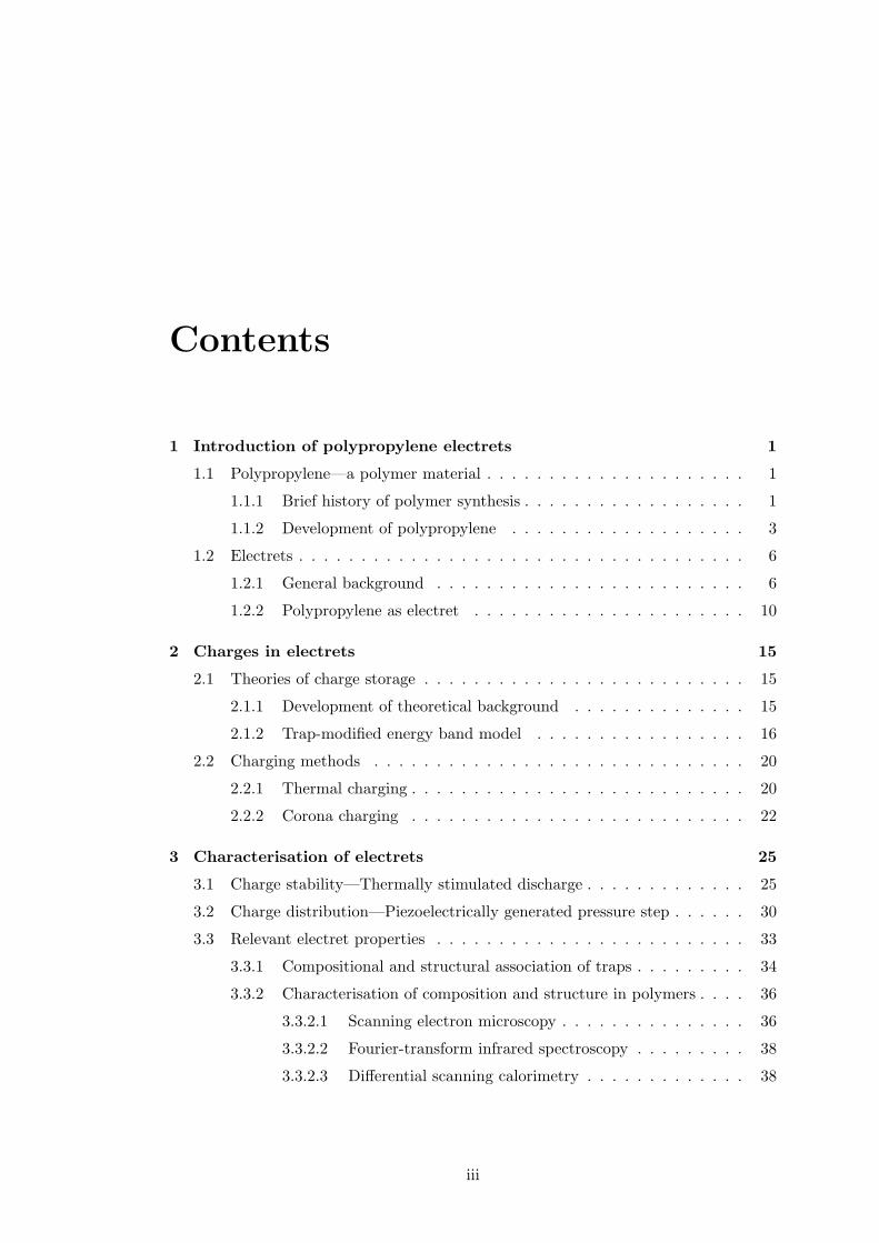
Figure 1.4: A schematic diagram of the charging process in a single void -
(A) When the charging voltage reaches the threshold value (Vthr), Paschen breakdown is
ignited. (B) At higher voltage, a second discharge may occur. (C) The reverse electric field
from captured charge may result in a back discharge as the applied voltage decreasing.[41]
An “electrothermalmechanical” film made from the cellular biaxially-oriented PP
was introduced by Savolainen and Kirjavainen in 1989 [40]. The “electrothermalme-
chanical” effect of the particular cellular PP film was essentially the ferroelectricity.
The ferroelectric property, as mentioned above, is caused by the aligned dipoles in
10

1.2 Electrets
the material. Hence, the idea of ferroelectricity in a non-polar material without any
molecular dipoles is rather counterintuitive. The secret lies in the cellular structure
of the PP films. As illustrated in Figure 1.4 [41], the Paschen breakdown occurs in
the voids when the cellular film is subjected to a sufficiently high electric field, turn-
ing the voids into small plasma chambers. Positive and negative charges travel under
the electric field to the opposite directions and are captured by the inner surfaces of
the voids. The charges of different polarities are separated by the height of the void,
forming a macroscopic dipole. This type of non-polar films with the spontaneous po-
larisation of void-dipoles are termed “ferroelectret” in order to be distinguished from
the ferroelectrics with intrinsic molecular dipoles [18].
The dipole moment (µ) in any ferroelectric material regardless of molecular or
macroscopic dipoles is the product of the separated charges (q) and the length of the
dipole (l):
µ = q · l. (1.1)
The overall spontaneous polarisation (P ) responsible for the ferroelectricity is reflected
in the sum of the dipole moments:
P = n · µ · 〈cosϑ〉, (1.2)
where n is the density of dipoles, and ϑ is the angle between P and µ. In the case
of polymer ferroelectrics, the dipoles consist of the covalent bonds between the car-
bon atoms and they are stronger than the interaction among dipoles. The external
compressing or expanding forces can only change the distance between dipoles, hence
the dipole density n. On the other hand, the contraction or expansion on the cellular
ferroeletrets primarily causes the deformation in the voids, leading to changes in the
length of the dipoles (l). Here the polarisation is decreased or increased with the dipole
moment (µ). Conversely, applying voltage across either the ferroelectric or the ferroele-
tret films can induce changes in their thickness or in the pressure that they exert onto
the adjacent space [18].
The effects of the ferroelectrics and ferroelectrets are united by Gerhard, Bauer,
and Qiu into one “charge-spring model”. The concepts of the dipole and its surround-
ings are set aside in the model, and the entire piece of the ferroelectric or ferroelectret
material is viewed as charges connected with springs of different spring constants in-
stead (illustrated with a schematic diagram in Figure 1.5). The model can predict the
11

1. INTRODUCTION OF POLYPROPYLENE ELECTRETS
piezoelectric response of the polymer ferroelectrics (PVDF), ferroelectrets (PP foam)
and even ferroelectric perovskite (PZT) with the corrected spring constant [42, 43].
In comparison to the PVDF and PZT ceramic ferroeletrics, the PP cellular ferro-
electrets have much lower density and better coupling efficiency to gases on account
of the air content in the voids. The small pyroelectric coefficient gives the PP cellular
ferroelectrets high piezoelectric sensitivity. The ferroelectret-based electronic skin and
large-area touchpad were reported. And the material is also suitable for the air-borne
ultrasound detection and nondestructive testing applications [44, 45]. The development
of the ferroelectret concept has extended to different materials and structures, the cel-
lular foam-like and tubular-channel ferroelectrets with FEP were successfully built and
investigated [46, 47, 48]. Although the charge retention ability of the PP foam is not
as excellent as that of FEP, it is still favoured for its low material cost and simpler
foaming process.
Figure 1.5: A schematic illustration of the charge-spring model for elastically
heterogeneous dielectric materials. - The piece of dielectrics consists of a matrix
phase, a dipole phase, and interface charges of opposite polarities between them [42].
Without the contribution of the cellular structure, PP can also be employed as a
space-charge electret material. Prior to the ferroeletret foam application, PP electret
was first used in the electret filters, which are gas filters consisting of fibres carrying
electric charges. It is the essential component in the particulate-filtering facepiece
respirators (e.g. the N95 type). As shown in Figure 1.6, the fibres are bipolar-charged
12

1.2 Electrets
and pressed into randomly oriented fabric webs. The electrostatic field generated by
the filter in its vicinity can attract the incoming particles with a long-range interaction
of a strong electrical force. It works in a similar way that a magnet attracts the iron
particles: the charged particles are drawn towards the electret filter by the Coulomb
force and the uncharged particles by the inductive force. This mechanism allows the PP
electret fabric webs to be made less dense than the conventional mechanical fibrous-
filters, so that the resistance to the gas stream can be reduced while the filtration
efficiency for sub-micron particles remains the same or even increases [33, 49, 50].
However, in both the cellular ferroelectret and electret filter applications, PP shows
its limitation in terms of the surface charge stability. This issue will be addressed in
chapter 4 - 6 of the thesis.
+ ++
+
+
++
+ + + +
+++
++
++
++
+
−−−
−−
−
−−
−−
− − −−
−
−−
−− − −
−+−
+−+
charged fibre
Figure 1.6: A schematic illustration of the fibrous electret filter. - The bipolar
charged PP fibres can attract particles with a long-range interaction to achieve a higher
filtration efficiency with much lower air resistance [33].
13
1. INTRODUCTION OF POLYPROPYLENE ELECTRETS
EMPTY PA
GE
14

2
Charges in electrets
2.1 Theories of charge storage
2.1.1 Development of theoretical background
Since the beginning of the systematic research on electrets in 1919, the theoretical
understandings of the charge storage in electrets have been developed along with the
applications. Shortly after Eguchi’s phenomenological investigations on the electret
behaviour in various waxes and rosins, Gemant confirmed Eguchi’s observation of the
polarity reversals in 1935 and introduced the term “homocharge” and “heterocharge” to
describe the charges of the same and opposite polarity to that of the adjacent electrode,
respectively [19]. Following their footsteps, Gross conducted a series of quantitative
experiments on carnauba wax in the 1940s. The coexistence of homo- and heterocharges
in the electret and the compensating mirror charges on the electrodes induced by the
sum of homo- and heterocharges were discussed. He also attempted to explain the
mechanism of the charge storage and found the existing theories of the ionic charge
carriers and dipole theories unsatisfactory [51, 52]. Later, Gerson and Rohrbaugh used
a collection of carnauba waxes with the different thicknesses and forming field strengths
to test the ionic space charge and dipole theories in 1955. They concluded that these
theories were not sufficient for explaining the existence of the homocharges in the
electret and proposed the “trap” theory. The theory suggested that the homocharge
carriers moved into certain “traps” simultaneously with the formation of heterocharges
and were released later upon heating. It was also pointed out that the trapping rate
15

2. CHARGES IN ELECTRETS
must show the temperature dependence [53]. The theory was first presented as a
tentative hypothesis and was later supported by Gross and Perlman [54, 55].
The electron trapping model was examined with X-ray radiated amorphous and
semi-crystalline polymers by Fowler [56]. In the same period, the theoretical fundamen-
tals of the impurity conduction in doped inorganic semiconductors were established:
an impurity conduction band was formed for the continuous charge transport, when
the concentration of the impurities was high enough to cause a strong overlap of their
states and overcame their localised characteristics. However, when the impurity con-
centration was below such threshold, a stochastic transport model of charge carrier
“hopping” from an occupied localised state to an unoccupied one was suggested by
Mott and Conwell independently in 1956 [57, 58, 59, 60, 61]. A trap-modified energy
band model for the charge storage and transport in polymer electrets was proposed by
Bauser in 1972, which combines the “trapping” and “hopping” theories [19, 62, 63].
The model is still well received today and will be introduced in section 2.1.2.
2.1.2 Trap-modified energy band model
As discussed in section 1.2, the typical origins of the electric charges in a polymeric
electret are the “true” polarisation and the “real” charge. The former is commonly
achieved by orienting the intrinsic dipoles under a sufficiently high electric field at
elevated temperatures and subsequently cooling them to freeze-in the alignment (the
so-called poling process). The total polarisation is the sum of the effective dipole
moments as shown in (1.2). Therefore, the apparent electric charges of the electret
are stored in the ordered arrangement of the dipoles, owing to the energy input during
the poling process. The aligned dipoles will thus have the tendency to relax into a
lower-energy state with a random orientation. The polarisation of the electret (Pd),
under isothermal conditions (T is constant), often decays in a classical thermodynamic
manner as a function of time (t):
Pd = Pd(t=0)exp(−α(T )t), (2.1)
in which α(T ) is the dipole relaxation frequency with a temperature dependence of
α(T ) = α0exp(Ai
kT). (2.2)
16

2.1 Theories of charge storage
The α0 and Ai are the frequency constant and dipolar activation energy, respectively
[19, 64].
It is rather straight forward to comprehend where and how the electric charges are
stored in the dipolar materials. However, when it comes to the “real” charges in the
non-polar polymeric electrets without the intrinsic charge carriers, the understanding
of charge storage and dissipation can be tricky. The excess charges deposited in the
electrets are known as the space charges (referring to both surface and bulk charges),
which can be found in the dipolar electrets as well. Hence, it is of great importance to
understand the mechanism behind the phenomenon.
In the description of the cellular PP ferroelectrets formation in section 1.2.2 and
in Figure 1.4, the term “capture” was used to refer the transfer of the positive and
negative charges from the plasma to the inner surfaces of the voids. In the trap-
modified energy band model proposed by Bauser, the space charges are captured by
the “traps” in the PP electrets [63]. The concept was derived from the energy band
theory of semiconductors. In semiconductors, when a molecular orbital is unoccupied,
it is a potential host for a negative charge; whereas if a molecular orbital is occupied
by an electron, it is a potential host for a positive charge, since a positive charge
is defined as the removal of one electron (named “hole”). The neighbouring lowest
unoccupied molecular orbitals (LUMO) will overlap to form the conduction band (Ec)
for electrons and the highest occupied molecular orbitals (HOMO) will form the valence
band (Ev) for holes. The negative (electrons) and positive (holes) charges can move to
the opposite electrodes along the conduction and valence bands, respectively, under the
electric field in an ideal semiconductor with a perfect periodic-lattice structure. But in
real semiconductors, impurities or structural defects can cause disruption of the energy
bands and perform as traps for the negative and positive charges. The trapping and
immobilisation of the charges may impair the charge transport of the semiconductor in
the photovoltaic or light-emitting diode, thus reducing the efficiency [65].
The concept of energy bands cannot be applied to the common polymeric electrets
directly, because the majority of the polymers are semicrystalline: the long chains of
polymer molecules are partially packed in a roughly ordered lamella structure in the
crystalline region and the rest are coiled randomly in the amorphous domains. Each
of the atoms or groups of atoms presents an individual state, due to the influence
of their surrounding environment. Their orbitals are not able to overlap and to act
17

2. CHARGES IN ELECTRETS
as a continuous conduction or valence band. Instead, there exists a distribution of
localised states near the mobility edges (Ev and Ec) and they behave in a very similar
way as the traps in the semiconductors. The energy diagrams for a polymeric electret
and the localised states are shown in Figure 2.1 [19, 62, 63]. To a certain extent, the
polymeric electret can be understood as a piece of semiconductor with a large amount
of “impurities” or “defects”, so that the entire continuous energy-band structure is
overthrown by the localised traps. When the electrets are poled by means of charge
injection or deposition, the excess space charges will be captured by these localised
states. The negative charges will be trapped near the Ec and the positive charges near
the Ev. The energetic difference between the trap and the nearest mobility edge (Ev
or Ec) is called the trap depth (Etrap).
Figure 2.1: The trap-modified energy band model - (a) The energy diagram for
a polymer electret; Te represents the electron traps and Th, the hole traps [63]. (b) The
density of states N(E) for a polymer electret. The localised states (traps) are shaded. Ec
and Ev are the mobility edges [19].
The space charges of the polymeric electrets are stored in the traps of “impurities”
in analogy to the semiconductors, ergo it is only sensible to use the “hopping” model
of the impurity conduction in semiconductors to describe the charge transport in the
real-charge electrets [58, 60, 63]. In Mott’s and Conwell’s models, the charges move
between the discrete traps by a hopping motion. The hopping transport of the space
charges involves the random diffusion due to the concentration gradient, the drifting
18

2.1 Theories of charge storage
process under the electric field, and the ohmic conduction. Only the drifting and ohmic
conduction are reflected by the current density (ic) through the electret:
ic = (g + µs+%s+ + µs−%s−) · E, (2.3)
where the µs± is the space-charge mobility and the %s± is the space-charge density, and
g is the ohmic conductivity. The process is driven by the internal electric field—E. The
term of the ohmic conductivity (g) in (2.3) is governed by the density of the intrinsic
charge carriers (n±) and their trap-modulated mobility (µ±) with
g = e · (n+µ+ + n−µ−). (2.4)
Both quantities are negligibly small in the electret-forming polymers, which are essen-
tially insulators. The excess space charges move under the electric field by the hopping
motion along the shallow traps near the mobility edges and are frequently captured
by the deep traps. The time (τ) of a charge spent in a particular trap before being
released is expressed as
τ = ν−1escexp(
Etrap
kT). (2.5)
The trapping time is influenced by the attempt-to-escape frequency (νesc), which is a
temperature-dependent factor, while it increases exponentially with the activation en-
ergy that is the trap depth (Etrap). Therefore, the life time of the charges is dominated
by the activation energy of the deep traps. Even if the charge first falls into a shallow
trap upon poling, it will soon escape from the shallow trap and likely be captured by
a neighbouring deep trap. As a result, the deep traps are mostly responsible for the
experimentally observed activation energy distribution in an electret [19, 66].
Commonly, the traps in the amorphous and semicrystalline polymeric electrets con-
sist of the structural and compositional disorders, which create energy barriers or dis-
ruptions with their own energy level that differs from that of their surroundings. The
traps in a piece of electret can be classified position-wise as the surface traps and bulk
(or volume) traps, and they are often associated with the impurities, morphology, and
chemical composition of the polymer molecules, etc. [66]. Furthermore, the fluctuation
of the polymer structure and conformation upon its temperature change can vigorously
impact the positional distribution and energy state of the traps. Thus, the thermal
properties of a polymer material also influence its electret behaviour [62]. The nature
of the traps in the polymers and their effect on the electret properties will be discussed
in section 3.3.
19

2. CHARGES IN ELECTRETS
2.2 Charging methods
Different charging methods are often required to obtain the dipolar and space-charge
electrets. Even with the same electret film, the result may vary significantly with
different charging conditions. The space charges in an electret can be either transferred
from the external sources or generated internally by certain stimuli. In the case of
external transfers, the low energy sources usually deposit the charges on the electret
surfaces, for instance, the triboelectrification [50], corona discharge [67], and dielectric
breakdown discharge of the cellular ferroelectrets shown in Figure 1.4 [41]. When
the high-energy electron or ion beams are employed, the charges can be injected or
bombarded into the bulk of the electrets [29, 30]. The mono-energy particle sources are
often chosen for a precise control over the penetration depth, i.e. the location of the
implanted charges.
For some electret materials, pairs of positive and negative charge carriers, i.e. the
excitons, can be generated under the harsh radiation of X-ray, β ray or γ ray. The
charge pairs are immediately separated by the electric field across the electret to avoid
the charge recombination [68]. A softer radiation source of ultraviolet or visible lights
can also generate the charge pairs in certain electrets named “photoelectrets”. The
internal charges might also originate from the impurities or triboelectrification during
the manufacturing procedures, which are screened by each other and only contribute to
the electret effect after being separated. Regardless of the origin of the charge pairs, the
separation process is otherwise the same as that of the X-ray radiated electrets [19].
The charge separation may be performed at elevated temperatures to accelerate the
process, which involves thermal charging. The principle and operation of the thermal
and corona charging will be introduced in section 2.2.1 and 2.2.2 below, respectively.
2.2.1 Thermal charging
The thermal charging is one of the oldest electret charging techniques, where an electric
field is applied to a piece of electret at a properly selected poling temperature, followed
by cooling with the field continuously present. The temperature and electric field
profiles during the thermal charging are presented in Figure 2.2. The method is widely
used for poling the dipolar electrets as discussed in section 2.1.2. For most of the
semicrystalline polymers, the poling temperature (Tp) is typically set above the glass
20
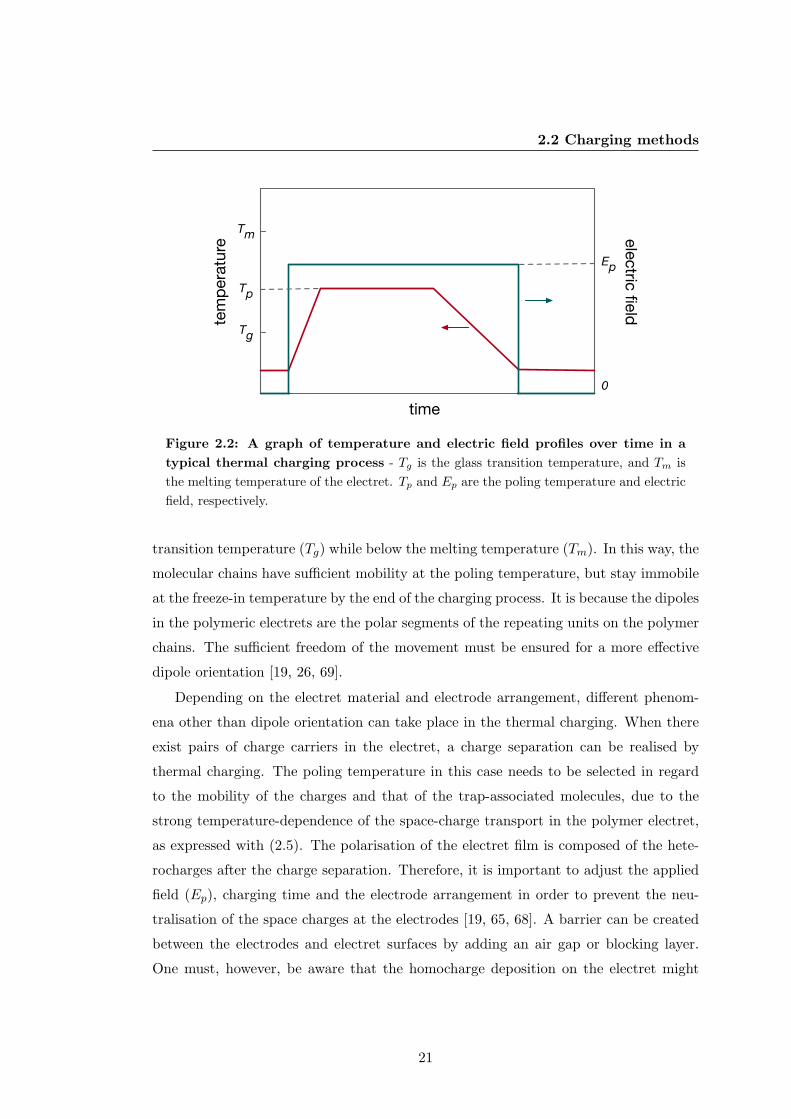
2.2 Charging methods
time
tem
pera
ture
Tm
Tg
Tp
electric field
Ep
0
Figure 2.2: A graph of temperature and electric field profiles over time in a
typical thermal charging process - Tg is the glass transition temperature, and Tm is
the melting temperature of the electret. Tp and Ep are the poling temperature and electric
field, respectively.
transition temperature (Tg) while below the melting temperature (Tm). In this way, the
molecular chains have sufficient mobility at the poling temperature, but stay immobile
at the freeze-in temperature by the end of the charging process. It is because the dipoles
in the polymeric electrets are the polar segments of the repeating units on the polymer
chains. The sufficient freedom of the movement must be ensured for a more effective
dipole orientation [19, 26, 69].
Depending on the electret material and electrode arrangement, different phenom-
ena other than dipole orientation can take place in the thermal charging. When there
exist pairs of charge carriers in the electret, a charge separation can be realised by
thermal charging. The poling temperature in this case needs to be selected in regard
to the mobility of the charges and that of the trap-associated molecules, due to the
strong temperature-dependence of the space-charge transport in the polymer electret,
as expressed with (2.5). The polarisation of the electret film is composed of the hete-
rocharges after the charge separation. Therefore, it is important to adjust the applied
field (Ep), charging time and the electrode arrangement in order to prevent the neu-
tralisation of the space charges at the electrodes [19, 65, 68]. A barrier can be created
between the electrodes and electret surfaces by adding an air gap or blocking layer.
One must, however, be aware that the homocharge deposition on the electret might
21
2. CHARGES IN ELECTRETS
occur due to the spark discharge in the air gap or blocking layer. This can be avoided
by choosing an appropriate poling field and/or a blocking layer with a higher dielectric
strength than that of the electret sample.
2.2.2 Corona charging
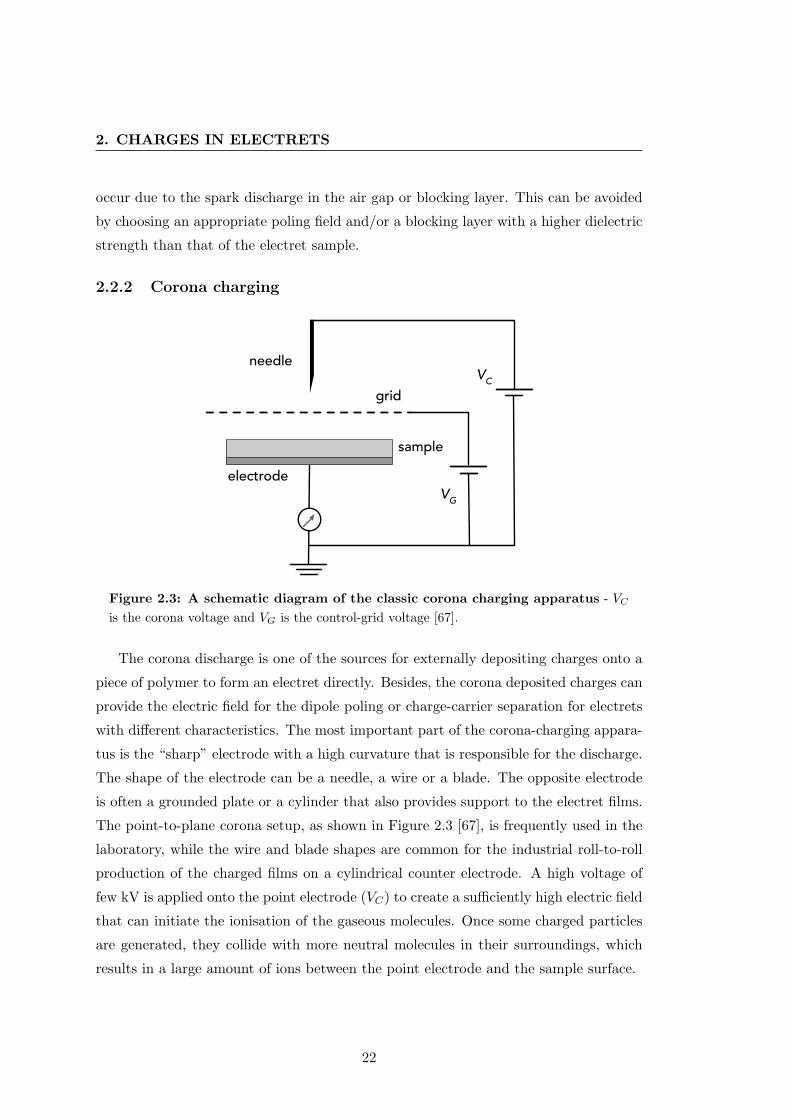
needleVC
electrode
sample
VG
grid
Figure 2.3: A schematic diagram of the classic corona charging apparatus - VC
is the corona voltage and VG is the control-grid voltage [67].
The corona discharge is one of the sources for externally depositing charges onto a
piece of polymer to form an electret directly. Besides, the corona deposited charges can
provide the electric field for the dipole poling or charge-carrier separation for electrets
with different characteristics. The most important part of the corona-charging appara-
tus is the “sharp” electrode with a high curvature that is responsible for the discharge.
The shape of the electrode can be a needle, a wire or a blade. The opposite electrode
is often a grounded plate or a cylinder that also provides support to the electret films.
The point-to-plane corona setup, as shown in Figure 2.3 [67], is frequently used in the
laboratory, while the wire and blade shapes are common for the industrial roll-to-roll
production of the charged films on a cylindrical counter electrode. A high voltage of
few kV is applied onto the point electrode (VC) to create a sufficiently high electric field
that can initiate the ionisation of the gaseous molecules. Once some charged particles
are generated, they collide with more neutral molecules in their surroundings, which
results in a large amount of ions between the point electrode and the sample surface.
22

2.2 Charging methods
The polarity of the charged particles solely depends on the polarity of the corona
voltage (VC), and the species of the ions are determined by the gas medium. When
the corona discharge is carried out in air, the prevailing negative ions are CO3−. The
positive corona can generate (H2O)nH+ in humid air (n increases with the humidity),
while (H2O)nNO+ and (H2O)n(NO2)+ begin to show dominance when the relative
humidity decreases to low values [70]. Unlike the ion beam charging method where
particles with the energy of keV magnitude strike and penetrate the electret surface,
the ions in the corona discharge only drift along the electric field extending from the
corona point to the sample surface, with energy comparable to that of the ambient
environment and a mobility of several cm2V−1s−1 [67]. Hence, the ions gently land on
the electret surface and their charges are captured by the traps on the surface, leaving
the neutralised molecules re-entering the environment. A well-controlled homogeneous
surface potential can be achieved with the aid of a wire-mesh, commonly known as the
control grid. It is positioned slightly above the electret surface with the same potential
(VG) as the desired value for the electret surface. The mesh allows the ions to pass
through, until a zero electric field condition is created between the grid and the sample
surface to prevent further charge deposition when the surface potential of the electret
is built up to the potential of the grid [19].
The ions are not able to penetrate through the surface of the electret via a corona
charging, whereas the possibility of the deposited charges migrating into the bulk of
the electret depends on the properties of the material and the charging conditions
[19]. For instance, it was reported that the charge penetration into the bulk of PP
electrets did not occur when it was corona charged at room temperature [71]. The
same observation has been made on FEP as well. However, if the corona charging of
FEP is implemented at an elevated temperature for a longer duration, the deposited
charges can drift into the electret film under the internal electric field. This can result
in a uniform charge spreading through the bulk of the FEP electret [72]. Furthermore,
the dipolar electrets like PVDF can be effectively poled with a corona setup as well
[69, 73]. These methods marry the corona charging with the thermal charging for
various outcomes. The corona charging technique can also be incorporated with the
charge and potential measurement setups in order to monitor the charging process and
charge transport in electrets [67, 74, 75].
23

2. CHARGES IN ELECTRETS
EMPTY PA
GE
24
3
Characterisation of electrets
3.1 Charge stability—Thermally stimulated discharge
After the charges are introduced in an electret with a proper charging method, the first
question at this point would be how stable the charges will be. The level of charge
stability is vital for an electret with space charges or molecular dipoles, because it
directly influences the possible life time and service conditions of the electret devices.
In the trap-modified energy-band model, the life time of each individual charge is
determined by the temperature and the activation energy (Etrap) of the trap (2.5).
When a charge acquires sufficient energy to overcome the barrier of Etrap, it can escape
the trap and drift in the local electric field. The process will lead to a current or a
potential decay in the electret as an external response of the charge dissipation. The
charge stability of an electret is a macroscopic concept, which is often described with an
energetic distribution of the traps. Generally, when the electret charges are subjected
to a scan of the input energy, a spectrum of the external current or potential decay in
respect of de-trapping energy can be obtained. The energy input is typically a photo-
or thermal-stimulation.
The photo-stimulated discharge (PSD) spectrum was used by Brodribb et al. in
1973 for the examination of the trapped charges in the single-crystal anthracene and
other insulators [76]. In the early 2000s, Mellinger employed the technique in the ultra-
violet (UV) range to measure the trapping parameters of a series of polymer electrets
[77, 78, 79, 80, 81]. The PSD method has the advantage of a wider-range energy scan
and a more precise control over the input energy resolution with the monochromatic
25

3. CHARACTERISATION OF ELECTRETS
light sources. However, it also presents several difficulties. The experiment needs to
be performed in ambient environment for the space-charge electrets, especially for the
surface-charge electrets, where the UV light is often scattered by the air. Although the
polymeric electret films are quite thin, it may still have some issue of the non-uniform
light absorption with different penetration depths [82]. In addition, it has been reported
that the photocurrent in UV range due to the photoelectric effect of the electrode can
interfere with the real current of de-trapping charges in the electret [83]. The PSD mea-
surement was initially introduced to complement the thermally stimulated discharge
(TSD) method, which had been applied extensively in electret studies [54, 55, 84].
The temperature of the electret film is increased linearly in a TSD measurement.
During the heating, the space charges become mobile and will be neutralised either at
the electrodes or within the sample. Since the 1970s, the TSD measurement was widely
used on both the dipolar and space-charge polymeric electrets. Different techniques and
better theoretical understandings were developed [33, 64, 66, 85, 86]. In a short-circuit
TSD, where the electret film is sandwiched between two connected electrodes, a current
can be detected in the external circuit as the consequence of the charge de-trapping. If
the electric charges are located on the electret surface, an open-circuit TSD can be used
to protect the surface charges. In the open-circuit TSD current measurement, one of the
electrodes is not in direct contact with the sample surface, but slightly lifted with a very
thin air gap in between. In this way the discharge can still be monitored with the change
of the compensating charges on the electrodes. The same current-temperature plots,
in principle, can be extracted with the open-circuit TSD measurement. However, the
air gap might introduce some variables and unknown factors, from which the accuracy
of the results may suffer. In the case of surface-charge electrets, the non-contact TSD
potential-decay measurement is a more reliable choice.
The TSD potential-decay setup consists of a heating system that increases the
temperature of the electret film at a constant rate and a Kelvin vibrating capacitive
sensor (Kelvin probe) as the detector of the potential decay in the sample [87]. The
Kelvin probe is essentially an electrode of small area placed near the open surface of
a single-side metallised thin-film electret, which is either mechanically excited with a
dynamic vibration or periodically shielded with a rotating shutter. The metal electrode
of the electret and the probe electrode with the electret and thin air gap in between
form a parallel-plate capacitor. Compensating charges are induced on the electrodes
26

3.1 Charge stability—Thermally stimulated discharge
due to the electric field of the electret charges. The vibrating or shielding motion alters
the electric field acting upon the probe and thus changes the induced charges on the
probe, which is detected as an AC voltage. The Kelvin probe was used to measure the
electrical polarisation of thin dielectric materials by Tyler et al. in 1955 [84]. In their
experiment, the alternating voltage was directly measured by a vacuum-tube voltmeter,
which is often referred as the dynamic-capacitor method. However, this method requires
an accurate control over the distance between the probe and the electret surface. To
overcome the limitation, instead of measuring the AC voltage directly, a DC voltage can
be applied to the probe to compensate the induced voltage and to nullify the electric
field in the air gap. By monitoring the compensating DC voltage, one can easily obtain
the value of the induced voltage on the Kelvin probe [19].
Vdc
probe
shield
metallisedelectret
heating system
Figure 3.1: A schematic illustration of the open-circuit thermally stimulated
discharge (TSD) potential measurement apparatus - Vdc is the compensation DC
voltage, which is equal to surface potential (V ) of the electret.
A general schematic diagram of the setup for the compensation TSD method is
illustrated in Figure 3.1. In this method, the voltage applied on the probe (Vdc) changes
with the potential on the tested surface (V ) and the potential decay of the electret can
be obtained as a function of temperature [88, 89]. The effective surface-charge density
27

3. CHARACTERISATION OF ELECTRETS
(σ) of the space-charge electret follows
σ = ε0εV/s, (3.1)
where ε is the relative permittivity of the measured electret material and s is the
thickness of the electret film. The discharging current (I) in the electret sample can be
calculated from the rate of the potential decay as
I = CairdV
dt= Cairβ
dV
dT, (3.2)
in which Cair is the capacitance of the air gap between the Kelvin probe and electret
surface, and β is the linear heating rate of the thermal stimulation. The non-contact
procedure of the TSD potential-decay measurement can minimise the disturbance on
the electret surface [19].
Many parameters regarding the electret properties of the measured material can be
extracted from the TSD results. For the molecular-dipole electrets, the theoretical eval-
uation and models of the TSD method were extensively studied and introduced by van
Turnhout in [64]. In the case of space-charge electrets, such as PP, the most commonly
evaluated quantities are the activation energy (Etrap), the attempt-to-escape frequency
(νesc), and the energetic trap distribution (N(Etrap)). Thermodynamic models are of-
ten used to describe the progressive charge de-trapping in polymer electrets. Almost
all such models operate on the basis of a fundamental condition: the thickness of the
electret sample (s) is much smaller than its other dimensions, so that the parameters
(electric field, charge density, etc.) are functions of the distance to the surface only.
In Kelvin probe TSD, the boundary conditions are electrical grounding at the lower
surface and zero electric field at the upper surface [88].
As introduced in section 2.1, the trap-modified energy band model considers that the
charge transport is restricted to hopping between shallow traps at the transport states
[63]. It implies that the charge transit time is much smaller than the mean characteristic
de-trapping time, so that the geometric factors can be eliminated. The potential decay
is mainly determined by the de-trapping kinetics. Another reasonable assumption
is made for the discharge models of disordered media, like polymeric electrets: the
dispersive transport regards the trapping levels as a continuous energy distribution [61].
In addition, the Etrap is considered a demarcation energy, and any contribution from
traps with energy lower than Etrap can be neglected at the corresponding temperature.
28

3.1 Charge stability—Thermally stimulated discharge
It means that the Etrap is a line between occupied deep traps and shallow traps at
transport states [90].
Numerous models were developed based on above approximations. A de-trapping
controlled space-charge decay model, introduced by Simmons and Tam in 1973 [91]
and further evaluated by Watson in 1995 [92], connected the thermally stimulated
de-trapping current (I(T )) to the energetic trap distribution (N(Etrap)) of polymeric
electrets with:
I(T ) = CairβdV
dT∝ N(Etrap). (3.3)
One can obtain the trap distribution by plotting the thermally stimulated current
(or first-order derivative of the potential decay with respect to temperature (dV/dT ))
versus the energy (Etrap) that is converted from the temperature by:
Etrap = T (a · lg νescβ
+ b)− c. (3.4)
Because a (1.92×10⁻⁴), b (3.2×10⁻⁴) and c (0.0155) are constants, the Etrap is pro-
portional to T [91]. It is a simple and straightforward model to quickly evaluate the
trap-depth distribution in some polymeric electrets, including PP. However, it was
pointed out by Watson that the model, in comparison to a detailed numerical com-
putation, underestimated the density of shallow traps, since the re-trapping influence
during the charge drifting was not considered [90, 92].
The characteristic trap depth of PP electrets has been calculated based on different
models and experimental measurements. The value is often influenced by the methods,
manufacturer and/or sample preparations. It typically falls between 1.02 and 1.11 eV
[90, 93, 94]. The characteristic trap energy of the as-received PP electret used in this
thesis was evaluated with (3.3) and (3.4) in [95], and it was 1.05 eV. The present work
mainly focuses on the influence of different treatments on the electret behaviour of the
PP films, thus the change of the trap distribution is more relevant than the absolute
value of the trap depth.
The TSD results of the polymeric electrets present the charge-decay process with
respect to temperature, which makes it possible to correlate the charge de-trapping with
different movements of the molecular chains. For example, a decay in the polymeric
electret might be from local motion of a polar side group or a start of whole-chain motion
due to glass transition. These miscellaneous processes often take place at different
29

3. CHARACTERISATION OF ELECTRETS
temperatures, resulting in current peaks or potential decays at various locations on
the TSD curves. It is important for identifying the structural or molecular association
of the traps with each particular energy level, especially for the polymeric electret
materials with both dipolar polarisations and space charges, e.g. PET [64]. The TSD
result can be influence by the heating rate, since the polymer chains need time to
respond to the temperature increase. Therefore, it is necessary to keep the heating
rate consistent for comparing different measurement results. Furthermore, the concept
of Kelvin probe has been incorporated with atomic force microscope (AFM), leading
to a Kelvin probe force microscope (KPFM). The technique is used for mapping the
charge storage and monitoring the charge transport in a nanoscale on the surface of the
electrets, semiconductors, inorganic ferroelectric crystals, etc. [96, 97]. In the thin-film
polymeric electrets, the charge distribution and transport in the thickness direction are
of a broader interest. The methods for charge profiling over the thickness-axis of the
electret films will be discussed in the following section.
3.2 Charge distribution—Piezoelectrically generated pres-
sure step
The excess charges can be deposited on the surface or injected in the bulk of the
polymeric electret films by different charging methods. The charges are later captured
in the surface or bulk traps. For many polymers, the surface and bulk portions of
the films exhibit different properties, due to the film manufacturing procedures [98].
Therefore, identifying the location of the trapped charges is important for studying
the structural and compositional origins of the traps. In addition, many charging
techniques, such as the electron-beam charging and high-temperature corona charging,
require the close monitoring of the charging depth. Methods for measuring charge
distribution in the electret have been developed to meet the demands of microscopic
investigations on the electret properties.
Gross and de Moraes used a sectioning method to study the internal charge distri-
bution of the carnauba wax: the charged wax electret samples were cut into sections
of different thickness and measured with TSD method individually to obtain a charge
distribution in respect of the depth under the samples surface [54]. It is, of course,
a coarse method that involves some problems: first of all, the sectioning may destroy
30
3.2 Charge distribution—Piezoelectrically generated pressure step
some charges that are in contact with the blade. Besides, the method is only possible
for measuring thick samples, but not suitable for the thin-film polymeric electrets with
a typical thickness ranging from tens to hundreds of micrometers. Thus, many other
techniques have been developed for profiling the charge distribution in the thickness
direction of the thin-film electrets.
Most of the charge-profiling methods rely on the concept that the electret can
be virtually dissected by activating the sample “slice-by-slice”: the inhomogeneous
excitations of the charges are established across the sample thickness by means of a
sharp pulse or sudden step of a stimulus propagating or diffusing in time through the
electret film. The application of the heat pulse was proposed by Collins [99, 100] and
Lang [101, 102]. Sessler and coworkers suggested to use a virtual electrode of an electron
beam to sweep the charges distributed in the sample [103]. A method that involves
decomposing the electret film with a pressure wave was proposed by Laurenceau et al.
in 1976 [104]. A laser-induced pressure pulse (LIPP) method was introduced in 1982.
When a short (< 1 ns) laser pulse is applied to a graphite coated surface of the electret
sample, a recoil due to the ablation of the graphite layer can launch a pressure pulse into
the sample [105]. Other than the thermal expansion method, pressure pulses generated
by acoustic methods using a shock tube [104] or a spark gap [106] and pressure steps
with a short rise time produced by a piezoelectric quartz crystal were used to probe
the charge distribution in the polymeric electrets [107]. The last method is known as
the piezoelectrically generated pressure step (PPS) measurement.
A schematic diagram of the PPS set-up is illustrated in Figure 3.2 [69, 108]. The
cable-discharge generator on the left side can produce a square voltage step with a
duration of 100 ns that drives the piezoelectric quartz to exert a pressure wave in a
step function to the sample surface. If there are surface charges on the electret sample,
a spacer is placed between the charged sample surface and the rubber electrode to
protect the surface charges. An uncharged film that is identical to the tested polymeric
electret sample is usually used as the spacer for a better acoustic coupling. Furthermore,
the quartz-oil-sample-spacer-rubber sandwich structure is slightly pressed together to
optimise the acoustic contact between different layers. In this way, the pressure step
can travel through the sample and spacer with the velocity of sound and compress the
sample volume behind the front of the step wave. The inhomogeneous compression
of the electret film causes a motion of the electric charges trapped at the location
31

3. CHARACTERISATION OF ELECTRETS
I(t)
oscilloscopepre-amplifier
rubber electrode
spacer
metallisedelectret
silicone oil
metallisedquartz
cable-dischargegenerator
R2R1
Figure 3.2: A schematic set-up of a piezoelectrically generated pressure step
(PPS) method. - Pressure steps generated by the quartz travels through the sample and
compresses the sample volume with the bounded electric charges, causing a current signal
in the circuit.
where the front of the step wave passes. The movement of the charges in the sample
brings about a temporary rearrangement of the induced charges on the electrodes,
which can be detected as a current between the rubber electrode and the grounded
quartz metallisation facing the sample. Therefore, the current signal can be plotted
as a function of time (t) since the pressure step has entered the sample. The spatial
charge distribution versus thickness (distance to the rear electrode) of the electret film
can be obtained by scaling the time domain with the propagating sound velocity (c) of
the pressure step in that particular sample material.
The mathematical relations between the current response and the desired charge or
electric-field distribution can be derived from the first principles, which was explained
in detail by Gerhard in [109]. The resulting equations are applicable for analysing
the current signal collected from the pressure steps, pressure pulses and even arbitrary
pressure profile experiments. If a step function is used, as in the PPS technique, the
electric-field distribution of the sample can be determined directly from the observed
current signal [110]. An approximate relation of the short-circuit current, I(t), and the
electric field E(x = ct) at location x in a non-polar dielectric sample was shown as
I(t) =ε0εA
s∗(4
3+ε
3− 2
3ε)p
ρ0c· E(ct), (3.5)
where p is the amplitude of the pressure step and ρ0 is the density of the tested electret
32

3.3 Relevant electret properties
material. The geometric factor A is the active area of the quartz-oil-sample-spacer-
rubber structure, which is typically controlled by the the area of the rubber electrode
with a diameter of 4.5-5 mm. The other geometric parameter s∗ is the distance between
the quartz-electrode contacting the silicone oil and the rubber electrode, that is the
thickness of the sample and spacer in sum [108, 109]. The distribution of the electric
field and the electric charges can be expressed in simpler forms:
E(ct) = C1 · I(t), (3.6)
and
ρ(ct) = C2 ·dI(t)
dt, (3.7)
respectively. C1 and C2 are the experimental constants related to the electret material
properties (ε, ρ0, c), the pressure function (p), and the geometry of the set-up (A, s∗)
[110, 111]. The values of C1 and C2 can be obtained by calibrating the measurement
system with identical samples whose charge distributions are known. However, for
tracking the changes of charge distribution on one single sample or on multiple samples
in the same material and geometry, the exact values of C1 and C2 are not necessary,
as long as the measurement conditions are consistent for all tests.
The resolution of the PPS method relies on the rise time of the pressure step, which
is approximately 1 ns for the set-up used in the present work, and it is also limited
by the sound velocity of the sample material. For a typical PPS measurement, the
resolution is around 2 µm. Thus, the method is not suitable for the ultra-thin electret
films [69, 108, 110]. Because PPS is a non-destructive method, the charge distribution
of the electret sample can be probed with many pressure steps sent in sequence. A
better accuracy can be achieved by averaging the results collected from thousands of
pressure steps.
3.3 Relevant electret properties
As discussed in previous chapters, the dipoles in the polar polymers originate from the
electron withdrawing and donating effect between atoms with different electronegativ-
ities [20]. The traps for capturing electric charges in the inorganic semiconductors are
mostly from the energetic interruptions of the impurities and structural defects on the
conduction and valence bands. The nature of the traps in the polymeric electrets is
33

3. CHARACTERISATION OF ELECTRETS
much more complex. Early theories in the 1970s [112, 113] suggested multiple trapping
levels associated with different molecular structures in polymers. Recent developments
on the computer simulation of charge storage and transport in polymer electrets agreed
with some existing theories, but also offered additional deeper understandings on the
subject.
3.3.1 Compositional and structural association of traps
On the atomic level of the polymer molecules, the trap depth and binding force to
charges with different polarities are influenced by the electronegativity and size of the
atoms. One typical example is the fluorine atoms in PTFE. Recent computations by
Sato et al. [114] showed that the electron traps in PTFE have equal contributions
from the carbon and fluorine atoms, whereas the hole traps are mainly localised to
the carbon atoms in the backbone of the molecular chains. The high electronegativity
of fluorine atoms in the fluoropolymers is believed to cause their severe asymmetrical
stabilities for charges of different polarities: the negative charges are more stable than
the positive charges in the fluoropolymer electrets.
The influence of the chemical composition of the polymer chains on trapping en-
ergy extends to groups of atoms. Simulations run on cyclic transparent optical polymers
(CYTOP) with various end groups revealed the association between the depth of elec-
tron traps and the electron affinity of the end groups. The results were in qualitative
agreement, however not quantitatively comparable with the experimental data, because
the simulated molecules had only few repeat units standing alone without interaction
with the adjacent molecules. As a result, the shorter polymer chains in the simula-
tion experienced a stronger terminal effect from the end groups, due to the atomic
ratio of the end group and the whole molecule. In real polymers, the macromolecu-
lar chains always entangle with each other and form structures with various degrees
of order, which leads to heterogeneous local morphological populations, e.g. lamellar
crystallites, amorphous regions and interfaces [115].
It has been reported that the electret properties of polymers show a significant de-
pendence on the spatial conformation of the molecular chains and the packing density.
Based on the trap-modified energy band model (section 2.1.2) and the quantum me-
chanical principles, it was shown in [114] and [116] that the holes (positive charges) in
the PE electret hop between the localised states (traps) near Ev (mobility edge) created
34

3.3 Relevant electret properties
by the polaronic effect on the molecular chain. In the amorphous PE, the characteristic
length of the localised states for the hole transport roughly matches the Kuhn length
of PE chains. Kuhn length is the length of the hypothetical free-joined segments that
allows the polymer chain to be considered as a random-walk or self-avoiding walk model
[117]. In the crystalline region of PE, the trap-modulated hole mobility increases with
the length of the simulated molecular chains. It is worth noticing that, when the chain
length reaches the thickness of the lamellar crystallite in PE, the mobility and acti-
vation energy for the hole transfer are in reasonable agreement with the experimental
values. The computation results indicate the significance of the system morphology in
the electret properties of polymers. Similar phenomena were observed in experiments
on the polymer electrets with different crystalline structures [13, 118, 119]. Because the
morphology of the polymer electrets is determined by the folding and packing of many
molecular chains, the traps associated with the crystalline and amorphous structures
are highly sensitive to the chain mobility of the polymers. Therefore, given the sim-
ilar chemical composition and molecular structure, the polymers with higher thermal
stability generally have a better charge stability.
Besides the atomic composition and chain conformation, which are intrinsic proper-
ties of the polymer molecules per se, the traps of a polymer electret are highly influenced
by the impurities in the system. The impurities in a polymer can be the oxidation prod-
ucts, additives from the processing, by-products and catalysts from the polymerisation,
and even random chemical contaminations mixed into the system during the manufac-
ture. The traps from the chemical impurities in the polymeric electrets are usually
deeper than the traps formed by the morphological disorders, according to the com-
putation based on the density function theory (DFT) in [120]. The result shows great
consistency with the calculation by Bauser, which concluded that the traps associated
with structural defects are shallower than that with foreign chemicals [63]. Thus, in
order to improve the charge stability by increasing the trap depth of the space-charge
electrets, different types of “impurities” were intentionally and strategically introduced
to the polymers by chemical reactions [121, 122, 123], doping, and mixing nanoparti-
cles to form the nanocomposites, etc. [124, 125]. The impurities of foreign chemicals
and disorders on the polymer chains, such as double-bonds, chain ends and bulky side
groups, have the tendency to move to the surface during the film processing. There are
pronounced differences between the surface and bulk traps in many polymer electrets,
35

3. CHARACTERISATION OF ELECTRETS
for instance, PE, PET, FEP and PP [126, 127]. Therefore, the surface of the thin-film
polymers often plays an important role in terms of the electret properties, especially
for surface charges.
Owing to the aforementioned association between the traps and the compositional
and structural properties, characterisation on the material properties of the polymers is
often implemented in the electret research. The features on the surface of the polymer
film, which might serve as the potential surface charge traps, can be detected with the
scanning electron microscope (SEM). The contributions on deep traps from the impuri-
ties of foreign chemicals intentionally or accidentally introduced to the electret system
are identified with the Fourier-transform infrared spectroscopy (FTIR). In addition,
the differential scanning calorimetry (DSC) is commonly used to reveal the thermal
properties and degree of crystallinity of a polymer material, and the polarised light mi-
croscope (PLM) is a simple and quick method for observing the crystalline morphology
in polymers. The principle and purpose of the SEM, FTIR, DSC and PLM experiments
will be briefly introduced in the section below.
3.3.2 Characterisation of composition and structure in polymers
3.3.2.1 Scanning electron microscopy
SEM is an important and versatile tool for the high-resolution analysis of surfaces and
often used in electret studies. In electron microscopes, the role of the visible light
in the optical microscopes is played by the electron beam emitted from a thermionic,
Schottky or field-emission cathode source. The electrons are accelerated through a high
voltage difference for a high particle energy, typically ranging from 0.1 keV to 50 keV.
The higher the particle energy, the better the resolution the electron microscope can
potentially achieve. For changing the trajectory of the electrons to focus the electron
beam, electron-optical lenses with carefully shaped magnetic fields based on Lorentz
force are used to replace the transparent glass lenses in the optical microscopes. In SEM,
an additional set of scan coils and scan generator circuit is coupled to the instrument
for changing the trajectory of the incident beam to scan the specimen line by line.
An SEM is usually equipped with multiple detectors to monitor the particles emitted
from the specimen upon interactions with the primary electrons from the accelerated
electron beam.
36

3.3 Relevant electret properties
The particles emitted from the specimen typically consist of the secondary electrons
(SE), backscattered electrons (BSE) and Auger electrons. The SE are the electrons that
escaped from the atomic orbitals of the sample molecules upon the inelastic collision
with the primary electrons. The BSE are the decelerated electrons undergone multiple
scattering through large angles and energy losses, due to their elastic interaction with
the atomic nucleus. The energy of BSE ranges between 50 eV and the energy of the
original primary electrons, which is higher than that of the SE. When the atomic
electrons of a higher energy level are de-excited and fill the vacancies on a lower-energy
orbital caused by the primary electron interaction, the excessive energy of the atomic
electrons can be converted to X-ray radiation or transferred to other atomic electrons
and leave the specimen as the Auger electrons.
Based on the principle of the interactions, different properties of the surface can be
obtained by analysing the detected electrons. The SE are often collected on a tilt angle
to the specimen surface, so that the emission from small particles, edges and shadow
contrast are enhanced. Thus, the SE are very suitable for the investigation of the
surface topography. The detection of BSE also requires a tilt angle from the surface,
so it is possible to be used for the surface topographic studies. But most importantly,
the backscattering coefficient of the BSE shows strong dependence on the mean atomic
number of the local specimen, which manifests the contrast on the resulting image.
This allows phases with different elements to be recognised. The X-ray and Auger
electrons are mostly utilised for elemental analysis [128].
The resolution of SEM is directly related to the energy of the electron beam, but
it is also influenced by the density and quality of the specimen and imaging mode.
The SEM instrument used in laboratories usually can achieve resolutions of a few tens
or hundreds nanometers. The ultra-high resolution model available from Hitachi is
capable of achieving a resolution of 0.4 nm. The surface of the polymeric electrets
plays a significant role in terms of the electret properties as discussed in the previous
section. The high-resolution atomic analysis and surface topographic investigations on
thin-film polymer electrets were implemented with SEM, and some traps with greater
activation energies were attributed to the characteristics on the surface [70, 122, 129].
37

3. CHARACTERISATION OF ELECTRETS
3.3.2.2 Fourier-transform infrared spectroscopy
The atomic composition of a surface can be analysed with SEM in a very high spatial
resolution. However, it is a task for FTIR to examine how the atoms are connected and
which functional groups the atoms form. FTIR is a technique based on the vibrations
of the atoms in a molecule. The vibrations are caused by the atoms moving out of the
present plane or by varying the distance between two atoms (bond length). The former
movement is called “bending” and the latter “stretching”. Each particular type of
the atomic vibrations in a particular molecular environment requires a specific energy.
Therefore, when an infrared radiation is passing through a sample, some fractions of
the incident radiation will be absorbed at some particular energies, resulting in a FTIR
spectrum of the sample. The peaks in an absorption FTIR spectrum correspond to the
vibrations of the atomic groups in the sample.
The quality of the results depends on the sensitivity of the FTIR instrument and
the concentration of the atomic groups of interest. If the chemical composition of the
sample surface needs to be analysed, the attenuated-total-reflection infrared (ATR-
IR) spectroscopy is a suitable tool. The ATR-IR spectroscopy utilises the total inter-
nal reflection phenomenon: by adjusting the angle of the incident infrared beam, one
can manage to only allow the beam to penetrate a fraction of the wavelength beyond
the sample surface before being reflected to the detector [130]. In this way, only the
molecules on the sample surface participate in the measurement. The information of
the chemical composition of the electret surface can be collected, while that of the bulk
is excluded.
3.3.2.3 Differential scanning calorimetry
The thermal stability and characteristic thermal transitions of the polymer electrets are
critical for their performance in terms of the charge stability. For the thermal analysis
of polymer materials, DSC is one of the most widely used techniques. In DSC the
sample substance and the reference are subjected to a controlled temperature program,
while the heat flow into the sample and the reference pans are monitored. When a
thermal transition or a phase change takes place in the sample, more heat or less heat
will flow into the sample pan. The thermal properties of the sample can be extracted
from the difference in the heat flow rates of the two pans as a function of temperature
38
3.3 Relevant electret properties
[131]. The concept can be technically realised in two different ways, namely the power
compensation DSC and the heat flux DSC. The power compensation method is highly
sensitive and excellent for academic studies, but the calibration is not easy and it
frequently suffers from the unstable baseline. The heat flux DSC is more robust. The
simplest models of heat flux DSC are able to carry out tasks of qualitative controls and
the most sophisticated models can match the sensitivity of the power compensation
DSC [132].
The charge mobility and trap parameters of the polymer electrets are highly de-
pendent on the chain mobility. Characteristic temperatures for the molecular chain
mobility in polymers can be obtained with the DSC measurements: the glass-transition
temperature (Tg), the melting temperature (Tm) and the crystallisation temperature
(Tc). The crystallinity (Xc) of the sample, that is, the percentage of the crystalline
phase in the polymer, can be calculated from the enthalpy of fusion (melting) (∆Hf )
during the DSC test, based on
Xc =∆Hf
∆Hf100· 100%. (3.8)
The ∆Hf100 is the enthalpy of fusion in a 100% crystallised sample of the same polymer
material [133].
3.3.2.4 Polarised light microscopy
The structure of the crystalline and amorphous regions can be directly observed with
PLM. A PLM is a transmission optical microscope equipped with a rotatable stage, a
polariser in the illumination system, and an analyser between the objective lens and
the eyepiece. The polariser and analyser are polars, which can selectively transmit
light that is polarised in one specific plane. The transmitted polarisation planes of the
two polars are usually placed to be perpendicular to each other, that is the so-called
“cross-polars”. With such arrangement, the view of an ideal isotropic specimen will
be completely dark, because the analyser cannot transmit light that has come through
the polariser. However, when a birefringent material (anisotropic) is subjected in the
view of PLM, the light waves passing through the sample can be considered as divided
into two polarisation planes that vibrate at a right angle to each other. Thus only a
fraction of the light from the illumination source can be transmitted via the analyser
to the observer [134].
39

3. CHARACTERISATION OF ELECTRETS
The most typical crystalline structure in polymers is the spherulite, which appears
as a bright “Maltese cross” with the arms lying parallel and perpendicular to the
extinction direction of the polars under PLM, as shown in Figure 3.3 [135]. The cross
figure remains stationary upon rotating the specimen in its own plane, implying the
radiating units of the polycrystalline spherulite are crystallographically equivalent. The
spherulites in polymers are composed of lamellar crystallites by fibrillation due to the
interfacial concentration instability [136] or by splaying and branching into multiple
generations of lamellae [137]. The polymer chains in the lamellae are usually packed
with the orientation perpendicular to the lamellae face, i.e. along the thickness direction
of the lamellae. Thus, the polymer spherulites are birefringent owing to the periodically
ordered microstructures. The refractive index of the birefringent spherulites depends
on the direction of the electric field in the light, which is the reason that the spherulites
appear as the Maltese-cross figures under the cross-polar PLM [134, 138].
Figure 3.3: Views of the spherulites of polypropylene under polarised light
microscope (PLM). - The spherulites grew in situ by isothermal crystallisation from
melt, and the images were taken after (1) 21.2 h, (2) 31.8 h, (3) 46.0 h, (4) 70.0 h. The
scale bar is 200 µm [135].
The resolution of the PLM is limited by the wavelength of the visible light, but it is
sufficient for visualising even small spherulites with diameters of several micrometers.
40

3.3 Relevant electret properties
PLM is a useful tool for analysing the morphology-related traps in polymers. If the
neighbouring spherulites are nucleated simultaneously, there will be a planar outline
between them. Otherwise, the boundary where they impinge is going to present a
hyperboloid of revolution [138]. It is possible to perform in situ crystallisation exper-
iments under PLM that has the incorporated heating system as illustrated in Figure
3.3. Many studies have been conducted with the aid of PLM, regarding the influence of
the size and density of spherulites on the electret properties of polymers [118, 139, 140].
3.3.3 State of the art on polypropylene electrets
The performance of the PP ferroelectrets and electret filters relies on the charge stabil-
ity. For enhancing the charge stability of PP, it is of great importance to understand
its charge storage and transport mechanisms. PP has one of the simplest composi-
tions among polymers but many versatile structures. Although it has one more methyl
group on the repeating unit than PE, PP films are believed to be cleaner than those
of PE. The structures of PP are very diverse in terms of the molecular tacticity, spa-
tial conformations and crystalline structures. Therefore, studying the correlation of the
compositional and structural properties to the parameters of the associated traps in PP
can be a fundamental step. It can offer a general guidance to modify any other existing
polymeric electret materials and to strategically design new materials or structures for
electrets. In addition, the charge storage and transport in PP is also extremely relevant
for its insulator applications [12].
The charge-mobility and electrical-conduction properties of PP were investigated
under DC voltages to mimic the environment of the HVDC cable insulation applications
[141, 142]. The pulse electro-acoustic (PEA) method was implemented to monitor
the charge transport under various electric field and at different temperatures [14,
143]. The storage and transport of the space charges trapped on the surface or in the
bulk of the PP films were modelled and experimented as well [144, 145]. The charge
trapping behaviour and charge distribution were significantly influenced by the chemical
composition of the PP molecular chains, i.e. PP as a homopolymer, block-copolymer
or random-copolymer with ethylene monomers [13, 14, 141].
The strong association of deep traps with the foreign chemicals in the polymeric
electret systems has been discussed in previous sections. The foreign chemicals usually
41
3. CHARACTERISATION OF ELECTRETS
consist of the impurities mixed into the system during manufacturing and certain chem-
ical structures that are intentionally introduced to the electret by chemical treatments.
Experiments with wet treatments and molecular-layer depositions on the surfaces of
fluoropolymers have shown promising results. The chemical treatments were able to
close the gap of the charge stability between positive and negative charges on PTFE
and FEP surfaces [121, 146, 147]. The studies of the influence of titanium tetrachloride
(TiCl4) and orthophosphoric-acid (H3PO4) treatments on the surface charge stability
have been extended to LDPE electrets as well. The treatments can increase the thermal
stability of both the positive and negative surface charges on LDPE films by at least 40
K. The significant improvements were attributed to the newly-formed deep traps from
the “island” structure of foreign chemicals on the treated surfaces [122, 148].
Similar liquid and gas treatments were carried out on PP cellular ferroelectrets with
the hydrofluoric acid (HF) solution and fluorine (F2) gas mixture, respectively. Solu-
tions and gas mixtures with series of concentrations, different treatment conditions and
combinations of supplementary chemicals were experimented to optimise the modifica-
tion on PP. Good results were obtained on the PP cellular ferroelectrets, whose thermal
stability and piezoelectric activity were both enhanced. The improvement was due to
the increase of deeper traps for surface charge storage and the decrease of Young’s
modulus of the foam structure [149, 150, 151, 152, 153]. However, the fluorination with
HF and F2 might be hazardous. The fluorine in the treated PP electrets may not be
as stable as that in the fluoropolymers, which can be released to the environment more
easily. Besides the foreign chemical agents, plasma can also be used to treat PP elec-
trets. It was reported that the PP surface can be selectively functionalised with specific
oxygen-containing functional groups after the underwater plasma treatment [154].
The etching technique was used for studying the charge storage properties of PP
electrets, which utilised the different reactivities of the amorphous and crystalline
phases upon contact with strong acids, such as permanganic acid, chromic acid and
sulphuric acid. The method was primarily used to identify the traps associated with
amorphous and crystalline phases and their difference in the activation energy level. It
was reported that both the trap depth and trap density were influenced by etching on
the PP surfaces [123, 155]. However, the changes in the surface-trap parameters after
the etching treatment cannot be fully attributed to the removal of the amorphous phase
on the surface. It is because the etching processes also leave some chemical residues on
42

3.3 Relevant electret properties
the treated PP surface, which can serve as deeper traps to improve the surface charge
stability thereof [156, 157].
The etching method for correlating the activation energy of traps and their loca-
tions in spherulites was invasive and complex with the intertwined chemical effects.
Another technique was introduced in [118] using the Sudan-blue dye particles (with a
size of 2.7 µm). The oppositely charged dye particles were attracted by the electret
charges trapped in the spherulitic PP. The trap distribution on the spherulites can be
visualised under the optical microscope in this way, and the trap depth was examined
by means of thermal stimulation. It was concluded that the number of the shallow
traps decreased with the spherulite size increasing. There have been many discussions
regarding the contribution to charge trapping from the amorphous and crystalline re-
gions. It was discovered in the morphology studies of polymers that the surface of
the commercially produced polymer films were covered with a thin amorphous layer
[98, 158]. The surface and bulk traps in PP electrets were investigated in [127] with the
TSD current measurement incorporated with the corona charging and electron beam
charging, respectively. The energy and distribution of the traps on the surface and bulk
are influenced by their morphological differences.
The density and depth of the traps in the PP electrets are influenced by the size
and number of the spherulites, but also by the degree of crystallinity. The experi-
mental results show that the trap density usually decreases when the spherulites are
bigger in diameter and fewer in number [118, 144, 159]. The difference in the size,
number and crystallinity of the PP spherulites are commonly achieved by means of
mechanical and thermal treatments. The treatments include stretching the films to
different ratios, annealing at different temperatures [119, 160], isothermal crystallisa-
tion for longer or shorter times [161], cooling the sample from melt with various rates
[119, 159], quenching [162], or adding nucleating agents [139]. The charge storage and
transport properties of PP also vary with the type of spherulites (β or γ) that results
from the copolymerisation of PP with PE [13].
Besides the spherulite, there exists a less-common crystalline structure in PP called
“transcrystalline” [98, 156]. The transcrystalline structures of many polymers were
studied by the morphology and polymer composite communities [164, 165], after the
discovery of the transcrystalline structure of polyurethane in 1952 [166]. It is a sur-
face/interface crystalline structure that stems from the surface and grows along the
43

3. CHARACTERISATION OF ELECTRETS
Figure 3.4: Polarised light microscope (PLM) images of the transcrystalline
and spherulitic polypropylene. - Polypropylene crystallised against surfaces of PTFE
(left), FEP (middle), and Glass (right) [163].
normal direction of the surface without the lateral growth. The transcrystalline struc-
ture is often observed at the interface of the fillers and matrix in polymer composites,
due to the high concentration of heterogeneous surface nuclei. The hypothesis was first
proposed by Schonhorn [167] and later carefully examined and proved by Hata et al.
[163]. When a PP film is crystallised from melt against a moulding surface, different
crystalline structures can be formed depending on the concentration of the nuclei on
the moulding surface. If the surface-nucleus concentration is low, the crystallites of PP
can expand from the nucleating centre to all directions into the polymer film, resulting
in a regular hemispherical spherulitic structure (before the neighbouring spherulites
impinging). In the case of densely packed surface nucleating points, the crystallisation
can only propagate in the normal direction of the film surfaces, and any growth to
the lateral directions is forbidden by the immediate neighbour-nuclei. Thus, to some
extent, the transcrystalline structure in the PP films can be understood as a special
one-dimensional spherulite that originates from the surface and propagates solely on the
thickness direction of the film. Microscope images of transcrystalline and spherulites
of PP are shown in Figure 3.4 [163].
The heterogeneous nuclei on the moulding surfaces are provided by the surface
roughness: the surface nuclei concentration is high when the surface is rough and low
when it is smooth. The transcrystallisation phenomenon of PP is very relevant to the
electret research, because the most commonly used moulding surfaces for producing
transcrystalline and spherulitic structures are PTFE and FEP, respectively [163, 168].
When the PTFE and FEP films are thermally fused onto a PP film for building elec-
tret devices or used as a non-sticky substrate under the melted PP, different crystalline
44
3.4 Scope of the thesis
structures are formed in accordance to the moulding surfaces. Therefore, it is of great
importance to investigate the electret properties of these two different crystalline struc-
tures in PP films.
3.4 Scope of the thesis
In the present thesis, the influences of the foreign chemicals and morphological struc-
tures on the charge storage and transport of the PP films are discussed. The experi-
mental results and interpretations are based on the thin-film PP electrets, but also of
significant concern to polymeric electrets in general, especially polyolefin electrets.
In chapter 4, the effects of the surface chemical modification on PP electret film
with H3PO4 will be presented and analysed. The surface charge stability of the PP
electrets with and without the chemical treatment will be compared. The influences
of the treatment on the surface trap parameters, including the energy, density and
distribution of traps, will be presented. In addition, the mechanism of the deeper trap
formation associated with the chemical and physical modifications will be discussed,
which is necessary for the design and optimisation of PP electrets in the future.
Regarding the morphology-related electret properties of PP, the spherulites have
been extensively studied in the past decades. However, the effort devoted to the trans-
crystalline structure of PP electrets is insufficient in comparison. The charge storage
and transport behaviour of the transcrystalline PP will be investigated in comparison
with that of the well-known spherulites in chapter 5. The charge distribution under
different conditions in the single- and double-layer transcrystalline PP electrets will be
discussed in chapter 6. It can provide the important insights into the difference of the
charge trapping behaviour in the intra- and inter-crystalline (spherulitic) regions. The
research on the simple and highly-ordered transcrystalline structure can be a funda-
mental step for understanding the charge storage and transport in the semicrystalline
polymeric electrets at large.
45

3. CHARACTERISATION OF ELECTRETS
EMPTY PA
GE
46
4
Surface chemical modification of
PP electret
4.1 Chemical treatment on PP surface
4.1.1 Treatment procedure
The oriented PP films (OPP-TSS) with a nominal thickness of 50 µm are supplied by
Putz Folien. 10 nm chromium (Cr) and 100 nm aluminium (Al) were deposited on
one side (outer side of the film roll) of the PP films in the Leybold Univex 350 vacuum
system with the INFICON SQC-310 deposition controller for sufficient electrical contact
during the corona charging and electrical measurements. Some of the metallised films
were used as-received for reference, named “non-treated” samples, and the rest were
treated with H3PO4 on the non-metallised surface—the so-called “chemically treated”
samples.
The treatment was carried out with the arrangement in Figure 4.1: the open surface
of the PP film was covered with 12 ml of 85% H3PO4 solution from Carl-Roth and the
metallised surface was not in contact with the acid solution. Because of the excellent
chemical resistance of PP at room temperature, the treatment needs to be performed
at elevated temperature. The PP films and the H3PO4 solution were kept on the
heating system (PRAZITHERM) at 120 ◦C for 24 hours with a covering lid for safety.
Afterwards, the PP films were cooled slowly down to room temperature together with
the H3PO4 solution, and then thoroughly rinsed with distilled water to remove the
H3PO4. After the samples were dried overnight, they were annealed at 160 ◦C and
47

4. SURFACE CHEMICAL MODIFICATION OF PP ELECTRET
subsequently quenched to room temperature in order to eliminate any differences among
samples in their thermal history during the acid treatments.
one-side metallised PP
heating at 120 ℃
H3PO4 85% solution
cover
Figure 4.1: An illustration of the chemical treatment on polypropylene surfaces.
- The non-metallised surface of the PP film was covered with H3PO4 solution and the films
and chemicals are heated together at 120 ◦C for 24 hours.
4.1.2 Compositional and structural characteristics
The Bruker Alpha-P FTIR device was used in the ATR-IR mode to determine the
chemical composition of the sample surfaces. The resulting spectra can reveal the com-
positional information of the open surface of the PP films, while the spectroscopical
information of the sample bulk was excluded. The characteristic absorption bands at
the higher wavenumber range that represent the chemical groups of the PP molecules
remain at their positions after the chemical treatment. However, the baseline of the
spectrum of the chemically treated PP is “lifted” up between 900 and 1250 cm−1, which
can be observed in Figure 4.2. This wavenumber range coincides with the extra absorp-
tion band on the spectrum of the H3PO4-modified LDPE surfaces in comparison with
that of the non-treated ones. The band was attributed to the phosphorus-containing
structures on the treated LDPE [122]. But, unlike LDPE, isotactic PP exhibits its own
regularity bands in the range of 700-1400 cm−1 [169]. Therefore, in the case of the
chemically treated PP, the regularity bands and the extra absorption bands from the
chemical modification merge and appear as a lifting of the baseline.
For analysing the chemical compositions that contribute to this phenomenon, the
extra bands (red solid line with symbols) are isolated from the PP regularity bands and
shown in Figure 4.2. The absorption band between 900-1125 cm−1 represents the asym-
metric P−O−C stretching, while the 1050-1165 cm−1 band is from the aliphatic P=O
48

4.1 Chemical treatment on PP surface
stretching [130]. Such results indicate that the phosphorus- and oxygen-containing
functional groups from H3PO4 are covalently bonded to the PP molecules via chemical
reactions. The heating during the chemical treatment and the subsequent annealing
have no contribution in the change of the ATR-IR spectrum of modified PP, which is
explained in [95].
1 2 5 0 1 2 0 0 1 1 5 0 1 1 0 0 1 0 5 0 1 0 0 0 9 5 0 9 0 0 8 5 0
0 . 0 1
0 . 0 2
0 . 0 3
0 . 0 4
0 . 0 5
0 . 0 6
Abso
rbanc
e
W a v e n u m b e r ( c m - 1 )Figure 4.2: Attenuated-total-reflection infrared (ATR-IR) spectra of non-
treated and chemically treated polypropylene films. - The spectrum of the chemi-
cally treated PP (blue solid line) is lifted from the spectrum of the non-treated PP (black
dashed line), because of the extra absorption bands (red solid line with symbols) of the
phosphorus- and oxygen-structures.
Besides the absorption bands between 900 and 1250 cm−1 on the ATR-IR spectrum
of the H3PO4-treated surface, the phosphorus- and oxygen-containing groups also bring
some topographic features onto the PP surface. The micrographs of the PP surfaces in
Figure 4.3 were obtained using a Zeiss Ultra/plus 55 SEM, which exhibit the detailed
topographic feature of the chemically modified surface (b) in comparison with the
as-received surface (a) of the PP films. Because PP is an insulating material, the
surface under observation was previously coated with 5 nm of gold for the surface
conduction of the electron beam in SEM. As shown in Figure 4.3, the SEM image
of the non-treated PP surface is smooth without any special features. The surface
49

4. SURFACE CHEMICAL MODIFICATION OF PP ELECTRET
modified with H3PO4 displays the island-like structures with diameters of 90-450 nm
and number densities of 1.5-2.0 µm−2. Similar island structures were observed on the
H3PO4-treated LDPE surface as well [122]. The configurational and/or compositional
disorders at the phosphorus- and oxygen-islands can create the energetic disruption on
the band structure of the polymeric electrets and capture charges as deeper foreign-
chemical traps [95].
(a)
(b)
Figure 4.3: Scanning electron microscope (SEM) images of the non-treated
and chemically treated polypropylene surfaces. - (a) The smooth non-treated PP
surface without any special features; (b) The H3PO4-treated PP surface with island-like
structures.
The characteristic thermal transitions and degree of crystallinity of the non-treated
and chemically treated PP films were measured with a DSC set-up from NETZSCH
50

4.1 Chemical treatment on PP surface
0 2 0 4 0 6 0 8 0 1 0 0 1 2 0 1 4 0 1 6 0 1 8 0 2 0 0- 1 . 2- 1 . 0- 0 . 8- 0 . 6- 0 . 4- 0 . 20 . 00 . 20 . 40 . 60 . 81 . 0
Heat
flow (
mW/m
g)
T e m p e r a t u r e ( o C )
exo
endo
Figure 4.4: Differential scanning calorimetry (DSC) curves of the non-treated
and chemically treated PP films - The two curves (non-treated sample in dashed
line and chemically treated sample in solid line) are identical, which indicates that the
treatment and the subsequent annealing process do not influence the thermal properties
and crystallinity of the PP films.
(model 214 Polyma) under a heating and cooling rate of 5 ◦C/min. Approximately 5
mg of the sample was used in each DSC test. The DSC results of the non-treated and
chemically treated PP samples in Figure 4.4 indicate that the thermal properties of
the film are not influenced by the treatment. This is because only the surface of the
PP film was modified by the H3PO4 treatment, whereas the bulk as the majority of
the film volume remains at its original chemical composition. In addition, the thermal
process during the subsequent annealing and quenching procedures is very similar to
that during the manufacture (extrusion and film forming) of the PP films. Therefore,
the thermal transitions on the curves—melting and crystallisation—during the first
heating and cooling cycle of the non-treated and H3PO4-treated PP appear to overlap
completely with each other. It is also verified that the subsequent annealing of the
treated samples can eliminate any possible difference among the treated samples in the
thermal history during the treatment. The melting and crystallisation temperatures
(Tm and Tc) of the non-treated and chemically treated PP are extracted from the DSC
results and their degree of crystallinity (Xc) is calculated with (3.8), which are all listed
in Table 4.1. The differences between their Xc (1%) in the table is within the typical
51
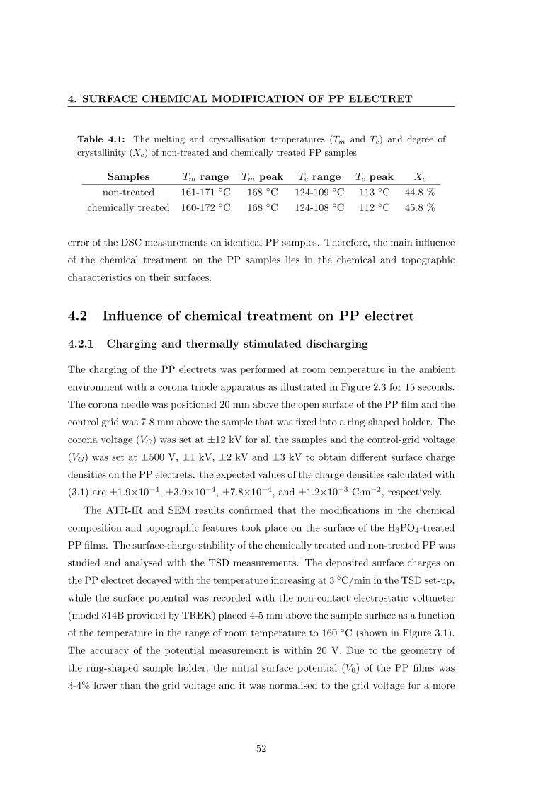
4. SURFACE CHEMICAL MODIFICATION OF PP ELECTRET
Table 4.1: The melting and crystallisation temperatures (Tm and Tc) and degree of
crystallinity (Xc) of non-treated and chemically treated PP samples
Samples Tm range Tm peak Tc range Tc peak Xc
non-treated 161-171 ◦C 168 ◦C 124-109 ◦C 113 ◦C 44.8 %
chemically treated 160-172 ◦C 168 ◦C 124-108 ◦C 112 ◦C 45.8 %
error of the DSC measurements on identical PP samples. Therefore, the main influence
of the chemical treatment on the PP samples lies in the chemical and topographic
characteristics on their surfaces.
4.2 Influence of chemical treatment on PP electret
4.2.1 Charging and thermally stimulated discharging
The charging of the PP electrets was performed at room temperature in the ambient
environment with a corona triode apparatus as illustrated in Figure 2.3 for 15 seconds.
The corona needle was positioned 20 mm above the open surface of the PP film and the
control grid was 7-8 mm above the sample that was fixed into a ring-shaped holder. The
corona voltage (VC) was set at ±12 kV for all the samples and the control-grid voltage
(VG) was set at ±500 V, ±1 kV, ±2 kV and ±3 kV to obtain different surface charge
densities on the PP electrets: the expected values of the charge densities calculated with
(3.1) are ±1.9×10⁻⁴, ±3.9×10⁻⁴, ±7.8×10⁻⁴, and ±1.2×10⁻³ C·m−2, respectively.
The ATR-IR and SEM results confirmed that the modifications in the chemical
composition and topographic features took place on the surface of the H3PO4-treated
PP films. The surface-charge stability of the chemically treated and non-treated PP was
studied and analysed with the TSD measurements. The deposited surface charges on
the PP electret decayed with the temperature increasing at 3 ◦C/min in the TSD set-up,
while the surface potential was recorded with the non-contact electrostatic voltmeter
(model 314B provided by TREK) placed 4-5 mm above the sample surface as a function
of the temperature in the range of room temperature to 160 ◦C (shown in Figure 3.1).
The accuracy of the potential measurement is within 20 V. Due to the geometry of
the ring-shaped sample holder, the initial surface potential (V0) of the PP films was
3-4% lower than the grid voltage and it was normalised to the grid voltage for a more
52

4.2 Influence of chemical treatment on PP electret
2 0 4 0 6 0 8 0 1 0 0 1 2 0 1 4 0 1 6 0
0
- 5 0 0
- 1 0 0 0
- 1 5 0 0
- 2 0 0 0
- 2 5 0 0
- 3 0 0 0
Surfa
ce po
tentia
l (V)
T e m p e r a t u r e ( o C )
Figure 4.5: Thermally stimulated discharge (TSD) curves of the negatively
charged non-treated and chemically treated PP electrets. - The plots of the
surface potential decay as a function of temperature in the non-treated (dashed line) and
chemically treated (solid line) PP films charged to −500 V, −1 kV, −2 kV and −3kV.
accurate data processing. Each TSD curve presented in the graphs was the average of
the results from 3-5 individual samples.
Samples with different surface potentials were measured with the TSD set-up to
investigate the influence of the surface-charge density on the H3PO4-treated and non-
treated PP electrets. The results of the surface-potential decay as a function of tem-
perature are plotted in Figure 4.5 for the negative surface charges and in Figure 4.6 for
the positive surface charges on the chemically treated (solid line) and the non-treated
(dashed line) PP electrets. It is obvious that the H3PO4 modification on the PP surface
can significantly improve its surface charge stability. The TSD curves of all the chem-
ically treated PP electrets are clearly shifted right to higher temperatures compared
to those of the corresponding non-treated PP in Figures 4.5 and 4.6. In addition, the
negative surface-charge stabilities are influenced more by the H3PO4 modification than
the positive ones.
One characteristic parameter commonly used for describing the charge stability of
an electret in the TSD measurements is the half-value temperature (T1/2). It is the
temperature where the surface potential decays to half of the initial value. The T1/2s
of all the chemically treated and non-treated PP electrets, as well as the improvement
53

4. SURFACE CHEMICAL MODIFICATION OF PP ELECTRET
2 0 4 0 6 0 8 0 1 0 0 1 2 0 1 4 0 1 6 0
0
+ 5 0 0
+ 1 0 0 0
+ 1 5 0 0
+ 2 0 0 0
+ 2 5 0 0
+ 3 0 0 0Su
rface
poten
tial (V
)
T e m p e r a t u r e ( o C )
Figure 4.6: Thermally stimulated discharge (TSD) curves of the positively
charged non-treated and chemically treated PP electrets. - The plots of the
surface potential decay as a function of temperature in the non-treated (dashed line) and
chemically treated (solid line) PP films charged to +500 V, +1 kV, +2 kV and +3kV.
of the T1/2 due to the treatment (∆T1/2) obtained from Figure 4.5 and 4.6 are listed in
Table 4.2.
The T1/2 of the non-treated PP electret decreases only slightly with the increase of
the initial surface potential (V0): it goes from 97 ◦C to 83 ◦C with V0 from −500 V to
−3 kV; and from 98 ◦C to 83 ◦C with V0 from +500 V to +3 kV. Moreover, the TSD
curves of the non-treated PP electrets from different V0s remain symmetrical for both
polarities. However, the chemically treated PP films respond differently to the negative
and positive surface charges. For instance, the TSD result of the H3PO4-treated PP
charged to V0= −500 V has a T1/2 of 144 ◦C, whereas that of the identical PP sample
charged to V0= +500 V only has a T1/2 of 136 ◦C. This leads to different degrees of the
enhancement brought by the chemical modification onto the PP electrets with negative
and positive surface charges, which are 47 ◦C and 38 ◦C at most, respectively.
The chemically treated PP electrets additionally experience more influence from the
increase of the initial surface potentials. From ±500 V to ±3 kV their T1/2 decreases
by 42 ◦C to 102 ◦C for the negative charges and by 41 ◦C to 95 ◦C for the positive
charges. With the non-treated PP electrets barely reacting and the chemically treated
PP electrets dramatically becoming less stable to the same initial-surface-potential
54

4.2 Influence of chemical treatment on PP electret
Table 4.2: Half-value temperatures (T1/2) of non-treated and chemically treated PP
electrets charged to different initial surface potentials (V0) and their differences (∆T1/2)
V0 Non-treated Chemically treated ∆T1/2
−500 V 97 ◦C 144 ◦C 47 ◦C
−1 kV 95 ◦C 140 ◦C 45 ◦C
−2 kV 91 ◦C 138 ◦C 47 ◦C
−3 kV 83 ◦C 102 ◦C 19 ◦C
+500 V 98 ◦C 136 ◦C 38 ◦C
+1 kV 96 ◦C 121 ◦C 25 ◦C
+2 kV 90 ◦C 113 ◦C 23 ◦C
+3 kV 83 ◦C 95 ◦C 12 ◦C
growth, the improvement of the T1/2 reduces to 19 ◦C and 12 ◦C for V0= −3 kV and
V0= +3 kV, respectively.
More importantly, in Figures 4.5 and 4.6, the chemically treated PP samples charged
to V0= ±3 kV are so unstable that their surface potentials at higher temperature range
drop below that of the identical PP samples charged to the lower V0 of ±2 kV, causing
their TSD curves to cross. This phenomenon is referred as the “cross-over”, which is a
typical behaviour of the LDPE electrets [170, 171, 172]. The discharge in the treated
PP electrets starts earlier when the initial surface potential is higher. The temperature,
where the potential decay of the chemically modified surface starts, decreases from 94
◦C for V0= −500 V to room temperature for V0= −3 kV. However, one must notice that
the surface potential of the H3PO4-modified samples with V0= ±3 kV appears to decay
in two stages. There are a faster decay at the lower temperature range before the cross-
over point and a slower decay at the higher temperature range that prevent the curve
from further crossing with TSD curves other than that of the V0= ±2 kV samples.
The two stages are better separated and easily observed when taking the first-order
derivative of the surface potential with respect to temperature (dV/dT ), as displayed
in Figure 4.7 for the negatively charged and in Figure 4.8 for the positively charged PP
electrets. The derivative curves are smoothed by means of the Savitzky-Golay method
to eliminate the noise from the overly dense data points.
The graphs of dV/dT versus temperature in Figure 4.7 and 4.8 represent the internal
drift-current plot based on (3.2) and the shape of the energetic distribution of the traps
55

4. SURFACE CHEMICAL MODIFICATION OF PP ELECTRET
in the PP electrets [91]. It is rather obvious that the derivative curves of both the
non-treated (dashed line) and chemically treated (solid line) PP electrets expand to
the lower temperature side as the initially deposited charge density increases. This
indicates that the charges in the electrets tend to fill in the deeper traps first and move
onto the shallower traps when there are no more deeper traps available [66], causing
the down shift of the T1/2 values with increasing V0. There are some differences in the
way that the trap distribution changes with the charge density for the non-treated and
chemically treated PP samples. The peak position of the derivative curve of the non-
treated PP remains at approximately 95 ◦C for V0 from ±500 V to ±2 kV and broadens
towards the lower temperature when V0 reaches ±3 kV. For the H3PO4-modified PP
electrets, there is only one peak at very high temperature when the samples are charged
to a low value of V0= ±500 V, and the peaks weigh more to the left when V0 is increased
to ±1 kV. With the V0 of the chemically treated PP reaching ±2 kV, their dV/dT
curves exhibit two peaks/shoulders at two temperature ranges: the left peak/shoulder
is located at ca. 95 ◦C which coincides with the peak position on the curves of the
non-treated PP; the right one appears at the same temperature range as the single
peak observed on the treated sample charged to ±500 V.
As suggested by the correlations of the peak positions, the two peaks on the curves
of the chemically treated PP charged to higher V0 are the results of the charge-escape
from two groups of traps: the deeper traps generated by the H3PO4 modification on the
PP surface, and the shallow traps that are intrinsic to the commercial PP films. The
chemical surface modification certainly formed a limited amount of deeper traps, while
the original traps of the PP surface were not completely erased from the treatment. This
agrees with the ATR-IR spectra and SEM images in the last section. The absorption
bands from the PP molecules are still intense on the ATR-IR spectrum of the treated PP
surface. Besides, only some discrete island-like structures, instead of a continuous new
layer, are observed on the treated surface under SEM. There is another strong evidence
of the contribution from the original shallow traps from the PP electrets. When the
peaks on the derivative curves of the non-treated PP weigh towards lower temperatures
as V0 reaches ±3 kV, the left peaks on the curves of the chemically treated samples
with the same V0 also moves together to the same lower temperatures. Thus, it can
be concluded that the intrinsic traps remaining on the H3PO4-treated PP surfaces are
56

4.2 Influence of chemical treatment on PP electret
2 0 4 0 6 0 8 0 1 0 0 1 2 0 1 4 0 1 6 0- 1 0
0
+ 1 0
+ 2 0
+ 3 0
+ 4 0
+ 5 0
+ 6 0
+ 7 0
+ 8 0
V 0 = − 2 k V
V 0 = − 5 0 0 VV 0 = − 1 k V
V 0 = − 3 k VdV
/dT (V
/o C)
T e m p e r a t u r e ( o C )Figure 4.7: First-order derivative of surface potential with respect to tempera-
ture (dV/dT ) of the negatively charged non-treated and chemically treated PP
electrets. - The dV/dT curves are obtained from the TSD measurements of the non-
treated (dashed line) and chemically treated (solid line) PP electrets charged to −500 V
(brown), −1 kV (blue), −2 kV (red) and −3kV (green).
responsible for the fast charge decay at low temperature when the surfaces are charged
to higher potentials.
The left-shift of the peak from the intrinsic shallow traps of the PP films happens
only when the V0 is as high as ±3 kV, which may explain the aforementioned cross-over
between the TSD curves of the treated samples charged to ±2 kV and ±3 kV. Not only
the deep traps introduced by the H3PO4 modification are not sufficient to host all the
deposited charges with the density of ±1.2×10⁻³ C·m−2 (V0= ±3 kV), but also the
original traps on the PP film surface cannot capture all these charges. As a result,
large fractions of the deposited charges in this case might be pushed into the bulk of
the film under the high internal electric field. In the bulk the traps may be shallower
and the charges may decay faster [172]. The charges on the non-treated PP samples
with V0 of ±2 kV are less stable and decay at lower temperatures. Thus, their TSD
curves do not cross with that of the non-treated PP with V0 of ±3 kV, and they overlap
instead. However, when deeper traps are created by the H3PO4 treatment on the PP
surface, more charges can survive till high temperatures on the treated PP charged to
±2 kV. Whereas many charges in the same PP with V0= ±3 kV are pushed into the
57
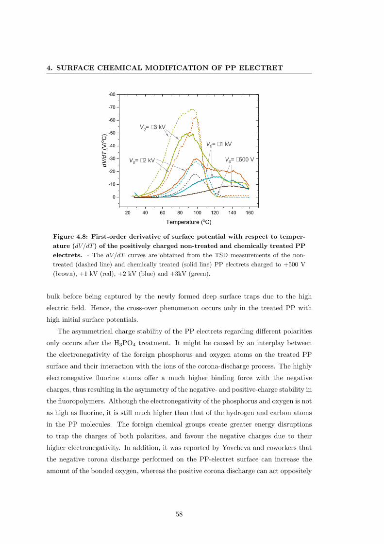
4. SURFACE CHEMICAL MODIFICATION OF PP ELECTRET
2 0 4 0 6 0 8 0 1 0 0 1 2 0 1 4 0 1 6 0
0
- 1 0
- 2 0
- 3 0
- 4 0
- 5 0
- 6 0
- 7 0
- 8 0
V 0 = + 5 0 0 V
V 0 = + 1 k V
V 0 = + 2 k VdV/dT
(V/o C)
T e m p e r a t u r e ( o C )
V 0 = + 3 k V
Figure 4.8: First-order derivative of surface potential with respect to temper-
ature (dV/dT ) of the positively charged non-treated and chemically treated PP
electrets. - The dV/dT curves are obtained from the TSD measurements of the non-
treated (dashed line) and chemically treated (solid line) PP electrets charged to +500 V
(brown), +1 kV (red), +2 kV (blue) and +3kV (green).
bulk before being captured by the newly formed deep surface traps due to the high
electric field. Hence, the cross-over phenomenon occurs only in the treated PP with
high initial surface potentials.
The asymmetrical charge stability of the PP electrets regarding different polarities
only occurs after the H3PO4 treatment. It might be caused by an interplay between
the electronegativity of the foreign phosphorus and oxygen atoms on the treated PP
surface and their interaction with the ions of the corona-discharge process. The highly
electronegative fluorine atoms offer a much higher binding force with the negative
charges, thus resulting in the asymmetry of the negative- and positive-charge stability in
the fluoropolymers. Although the electronegativity of the phosphorus and oxygen is not
as high as fluorine, it is still much higher than that of the hydrogen and carbon atoms
in the PP molecules. The foreign chemical groups create greater energy disruptions
to trap the charges of both polarities, and favour the negative charges due to their
higher electronegativity. In addition, it was reported by Yovcheva and coworkers that
the negative corona discharge performed on the PP-electret surface can increase the
amount of the bonded oxygen, whereas the positive corona discharge can act oppositely
58

4.2 Influence of chemical treatment on PP electret
[70]. When the surface of the PP film is not treated, the oxygen content is too low to
exhibit any pronounced asymmetry in the charge stability. However, on the H3PO4-
treated PP surface, the oxygen content is much higher and more critical for the charge
trapping at higher temperatures. So the asymmetrical charge stability for different
polarities is magnified by the chemical modification in this case.
4.2.2 Charge distributions during thermal discharging
The macroscopic electret properties of the non-treated and H3PO4-treated PP, includ-
ing the charge stability, influence of surface-charge density and polarity on the charge
decay behaviour, etc., were studied with the TSD measurements. Many important in-
formation related to the traps on the surface and in the bulk of the PP electrets with
and without chemical modification can be extracted from the results. The microscopic
pictures of the spatial trap distribution in the non-treated and H3PO4-treated PP films
are investigated with the PPS method.
The samples used in the PPS measurements were charged with a grid voltage (VG)
of ±2 kV for sufficiently high signal. To demonstrate the change of charge distribution
during the discharge process, the charged PP films were partially discharged with the
TSD set-up at the same heating rate of 3 ◦C/min to different critical temperatures:
R. T. (no thermal discharging performed), 60 ◦C, 90 ◦C, 120 ◦C. They were immedi-
ately quenched to room temperature to abort the discharging and to freeze the charge
distribution at that corresponding temperature. Samples discharged to different stages
are examined to illustrate the locations of the newly-formed deep traps and the charge
de-trapping and re-trapping during the TSD process. According to (2.5), the partial
thermal discharge can purge the traps with the activation energy below certain levels,
thus separating the shallow intrinsic traps and the deep traps from the chemical mod-
ification. The partial discharging was not performed on one sample in sequence, but
a piece of freshly charged new PP film was used for each partial discharge and PPS
measurement.
As shown in Figure 3.2, an uncharged clean PP film with a thickness of 25 µm was
used as a spacer to protect the charged sample surface from the rubber electrode. The
thickness of the sample films showed slight deviations from the nominal value, and thus
it had to be normalised to 50 µm. The final charge distribution results were averaged
from 4-7 individual samples. On the thickness axis, 0 was the metallised surface and
59

4. SURFACE CHEMICAL MODIFICATION OF PP ELECTRET
- 2 0 0 2 0 4 0 6 0 8 0- 1 . 2
- 1 . 0
- 0 . 8
- 0 . 6
- 0 . 4
- 0 . 2
0 . 0
0 . 2
0 . 4
n o n - t r e a t e d
V 0 = − 2 k V
Charg
e distr
ibutio
n (no
rmaliz
ed)
T h i c k n e s s ( µ m )
1 2 0 o C 9 0 o C 6 0 o C R . T .
o p e n s u r f a c e
Figure 4.9: Charge distributions of partially discharged non-treated PP elec-
trets with the negative corona charges. - The charge profiles in the thickness direction
of the non-treated samples charged to −2 kV. The curves are obtained from the samples
partially thermal-discharged to R. T. (non-discharged) (blue), 60 ◦C (red), 90 ◦C (green),
and 120 ◦C (black).
- 2 0 0 2 0 4 0 6 0 8 0
- 0 . 4
- 0 . 2
0 . 0
0 . 2
0 . 4
0 . 6
0 . 8
1 . 0
1 . 2n o n - t r e a t e d
V 0 = + 2 k V
Charg
e distr
ibutio
n (no
rmaliz
ed)
T h i c k n e s s ( µ m )
R . T . 6 0 o C 9 0 o C 1 2 0 o C
o p e n s u r f a c e
Figure 4.10: Charge distributions of partially discharged non-treated PP elec-
trets with the positive corona charges. - The charge profiles in the thickness direction
of the non-treated samples charged to +2 kV. The curves are obtained from the samples
partially thermal-discharged to R. T. (non-discharged) (blue), 60 ◦C (red), 90 ◦C (green),
and 120 ◦C (black).
60
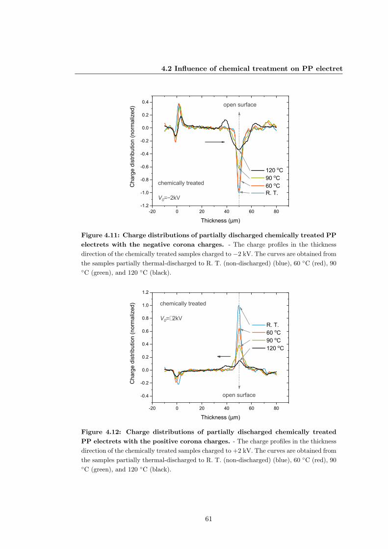
4.2 Influence of chemical treatment on PP electret
- 2 0 0 2 0 4 0 6 0 8 0- 1 . 2
- 1 . 0
- 0 . 8
- 0 . 6
- 0 . 4
- 0 . 2
0 . 0
0 . 2
0 . 4
c h e m i c a l l y t r e a t e d
V 0 = − 2 k V
Charg
e distr
ibutio
n (no
rmaliz
ed)
T h i c k n e s s ( µ m )
1 2 0 o C 9 0 o C 6 0 o C R . T .
o p e n s u r f a c e
Figure 4.11: Charge distributions of partially discharged chemically treated PP
electrets with the negative corona charges. - The charge profiles in the thickness
direction of the chemically treated samples charged to −2 kV. The curves are obtained from
the samples partially thermal-discharged to R. T. (non-discharged) (blue), 60 ◦C (red), 90◦C (green), and 120 ◦C (black).
- 2 0 0 2 0 4 0 6 0 8 0
- 0 . 4
- 0 . 2
0 . 0
0 . 2
0 . 4
0 . 6
0 . 8
1 . 0
1 . 2c h e m i c a l l y t r e a t e d
V 0 = + 2 k V
Charg
e distr
ibutio
n (no
rmaliz
ed)
T h i c k n e s s ( µ m )
R . T . 6 0 o C 9 0 o C 1 2 0 o C
o p e n s u r f a c e
Figure 4.12: Charge distributions of partially discharged chemically treated
PP electrets with the positive corona charges. - The charge profiles in the thickness
direction of the chemically treated samples charged to +2 kV. The curves are obtained from
the samples partially thermal-discharged to R. T. (non-discharged) (blue), 60 ◦C (red), 90◦C (green), and 120 ◦C (black).
61

4. SURFACE CHEMICAL MODIFICATION OF PP ELECTRET
50 µm was the charged open-surface of the PP sample. To better illustrate the charge
decay process, the vertical scale of charge density was normalised by the absolute value
of the surface charges without any partial discharge. It means that the amplitudes of
the peaks at 50 µm on the R. T. curves were all ±1.0, with the sign indicating the
polarity.
The charge distributions of the non-treated and chemically treated PP electrets are
illustrated for the negative and positive charges in Figures 4.9, 4.10 and in Figures 4.11,
4.12, respectively. From all four R. T. curves of the charge distributions in the figures,
it is clear that the corona discharge at room temperature only deposits charges on the
surface of the PP electrets without any injection to the bulk. The deposited charges
remain on the surface of the non-treated PP films till the end of the charge decay, as
demonstrated in Figure 4.9 and 4.10. The results agree with that obtained by Ono
and coworkers with the LIPP method in [71]. The peaks of the charge distribution
remain at the open surface (50 µm) of the non-treated films, though some slight peak
broadening is observed after the samples being partially thermally discharged to 90 ◦C.
The broadening might be the influence of the reduced signal-to-noise ratio due to the
lower surface charge density. Similar peak broadening effect after discharged to 90 ◦C
appears on the charge distribution curves of the chemically treated PP in Figure 4.11
and 4.12 as well.
Unlike the non-treated PP electrets, where no charge is present at 120 ◦C, there
are still significant amount of charges on the chemically treated PP films at the same
temperature (seen in Figure 4.11 and 4.12). It was demonstrated in Figures 4.7 and 4.8
in the previous section that the charges remaining at 120 ◦C are captured in the deeper
traps generated by the H3PO4 treatment. As shown in Figure 4.11, all the negative
deposited charges are trapped on the treated surface, indicating that the chemical
modification is restrained on the surface of the PP films without penetrating to the
bulk. The negative charges on the surface are not only stable enough to withstand
a temperature as high as 120 ◦C, but can also attract the opposite charges from the
rear electrode to travel through the bulk of the film and to build a layer near the
open surface, as illustrated with the arrow. The bulk portion of the PP film is not
treated with H3PO4, unlike the surface. Hence, the positive mirror charges on the rear
electrode can be easily transported to the open surface side in the same manner as that
in the non-treated PP electrets at 120 ◦C. In this case, the electric field of the remaining
62

4.2 Influence of chemical treatment on PP electret
surface charges on the treated PP acts as a high driving force for the positive charges.
However, the energy barrier created by the H3PO4-treated surface is strong enough to
block the positive charges from immediately neutralising the deposited negative charges
on the surface. Thus, a layer of the positive charges is still visible in the PPS results,
coexisting, at least temporarily, with the nearby negative charges on the sample surface.
The situation is different in the positively charged PP films treated with H3PO4.
First of all, the charge distribution curve at 120 ◦C in Figure 4.12 for the positive
surface charges exhibits peaks with much smaller area at the open surface than that in
Figure 4.11 for the negative charges. This result is consistent with the asymmetrical
charge stability observed in their TSD measurements. In addition, it can be seen that
the positive surface charges migrate further into the H3PO4-modified PP film at 120
◦C, appearing as a second peak near the surface, as indicated by the arrow. It shows
that the positive charges are able to acquire enough energy at this point to escape
the newly formed traps on the chemically treated PP surface. And they drift towards
the rear electrode under their own electric field, as opposed to the behaviour of the
deposited negative charges in Figure 4.11. The negative charge stability of the PP
electret is more influenced by the H3PO4 treatment than the positive charge stability,
which explains the difference in the ∆T1/2 in Table 4.2. At 120 ◦C, the positive corona
charges near the treated PP surface stay in two separate layers, appearing as two peaks
instead of merging into one wide peak on the PPS result. It once again shows the
barrier between the chemically modified surface and the non-treated bulk of the PP
films. This distinction reflects that treatment on the surface can bring about dramatic
improvement to the electret properties of the PP films, even though the majority of
the volume remains the same.
The experiments on the microscopic scale with the PPS method reinforce the in-
terpretation of the different binding force between the phosphorus- and oxygen-based
structures and the deposited charges of different polarities. The deeper traps associated
with these foreign chemical structures are negative-charge preferential, thus resulting in
the asymmetrical charge stability of the modified PP electrets. The phenomenon does
not take place in the non-treated PP samples where the foreign chemicals play only
a minor role in terms of charge trapping. Thus, it can be concluded that the foreign
chemicals in the treated PP electrets dominate the electret properties as the deeper
traps, which agrees with the results from [120] and [63].
63

4. SURFACE CHEMICAL MODIFICATION OF PP ELECTRET
Another phenomenon worth noticing from the PPS measurements in Figure 4.9 to
4.12 is that, at any point of the thermal discharge, there is no charge present in the
bulk of the non-treated or chemically treated PP film, except near the surface region.
It indicates that the charge re-trapping in the bulk does not occur during the charge
transport through the film volume. This means that the bulk traps are much shallower
than the surface traps. So they do not contribute on the life time of charges and the
spatial charge distribution as significantly as the surface traps when the samples are
charged to ±2 kV. Combining with the observation and analysis of Figure 4.7 and
4.8, the intrinsic traps, responsible for the low-temperature peak at ca. 95 ◦C, in
the H3PO4-treated PP with V0= ±2 kV are located on the surface instead of in the
bulk. On the other hand, when the modified PP films are charged to the higher V0
of ±3 kV, the shallower bulk traps start to participate in the charge storage. In this
case, the deep surface traps—both newly formed and intrinsic traps included—are not
able to accommodate all the deposited charges. It explains the cross-over phenomenon
observed in Figure 4.5 and 4.6, which is consistent with the interpretation in [172].
(a) (b)
Figure 4.13: Optical microscope images of the evaporated electrode on the PP
films with and without heating - Microscope images of the evaporated Cr/Al electrode
on the PP electrets before (a) and after (b) being heated to 90 ◦C.
Only the peaks of the charge distribution on the open surface side (at 50 µm thick-
ness) have been discussed and explained so far. However, the peaks of the compensating
charges on the rear electrode side (0 thickness) of the non-treated and chemically treated
PP films also exhibit some interesting variations at different discharging temperatures.
The abnormal double peak feature appears at the rear electrode for all the chemically
64

4.2 Influence of chemical treatment on PP electret
treated samples and the non-treated samples discharged to 90 ◦C, but not on the R. T.
and 60 ◦C curves of the non-treated PP. It is caused by the poor electrical conduction
of the evaporated electrode after being heated above 90 ◦C. When the non-treated PP
film is heated to 90 ◦C for the partial discharge or the chemically treated PP film is
annealed at 160 ◦C during the sample preparation, the oriented PP molecular chains
gain sufficient mobility to recoil from the stretched state. The evaporated electrode
is essentially a layer of metal particles attached onto the PP film, and it moves with
the molecules. This results in the patterned cracks on the electrode as shown in the
optical microscope images (Figure 4.13) of the electrode before and after heating to 90
◦C. The impaired electrical contact of the rear electrode causes the double peaks at 0
thickness on the charge distribution curves of the corresponding PP samples. The PPS
measurements can be carried out on samples without electrode, hence the damage of
the electrode on the PP films does not influence the reliability of the results for the
deposited charges on the open surface.
65

4. SURFACE CHEMICAL MODIFICATION OF PP ELECTRET
EMPTY PA
GE
66

5
Spherulitic and transcrystalline
PP electrets
5.1 Spherulitic and transcrystalline PP
5.1.1 Crystallisation of spherulitic and transcrystalline PP
PTFE/FEP
Al foil
FEP
PP 50 µm
50 µm
heat + pressure
heat + pressure
50 µm
PTFE/FEP
Al foilPP
template
Figure 5.1: A schematic diagram for the crystallisation of the spherulitic and
transcrystalline polypropylene - A piece of PP film placed between the moulding sur-
face of FEP or PTFE and Al substrate is melted and slowly cooled to form the spherulite
or transcrystalline structures with a template for thickness control.
The PP films supplied by Putz Folien with a nominal thickness of 50 µm were cut
into round pieces with a diameter of 60 mm. The moulding surfaces for the spherulitic
and transcrystalline structures were FEP (thickness of 127 µm) and PTFE (thickness of
67
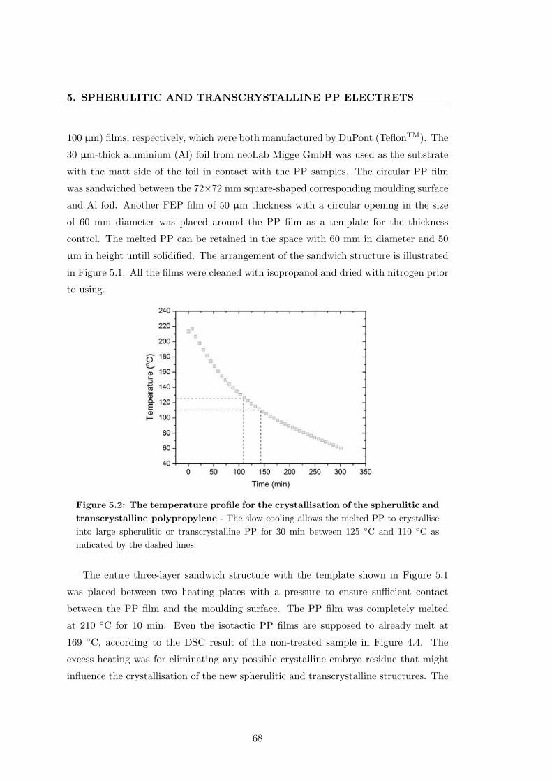
5. SPHERULITIC AND TRANSCRYSTALLINE PP ELECTRETS
100 µm) films, respectively, which were both manufactured by DuPont (TeflonTM). The
30 µm-thick aluminium (Al) foil from neoLab Migge GmbH was used as the substrate
with the matt side of the foil in contact with the PP samples. The circular PP film
was sandwiched between the 72×72 mm square-shaped corresponding moulding surface
and Al foil. Another FEP film of 50 µm thickness with a circular opening in the size
of 60 mm diameter was placed around the PP film as a template for the thickness
control. The melted PP can be retained in the space with 60 mm in diameter and 50
µm in height untill solidified. The arrangement of the sandwich structure is illustrated
in Figure 5.1. All the films were cleaned with isopropanol and dried with nitrogen prior
to using.
Figure 5.2: The temperature profile for the crystallisation of the spherulitic and
transcrystalline polypropylene - The slow cooling allows the melted PP to crystallise
into large spherulitic or transcrystalline PP for 30 min between 125 ◦C and 110 ◦C as
indicated by the dashed lines.
The entire three-layer sandwich structure with the template shown in Figure 5.1
was placed between two heating plates with a pressure to ensure sufficient contact
between the PP film and the moulding surface. The PP film was completely melted
at 210 ◦C for 10 min. Even the isotactic PP films are supposed to already melt at
169 ◦C, according to the DSC result of the non-treated sample in Figure 4.4. The
excess heating was for eliminating any possible crystalline embryo residue that might
influence the crystallisation of the new spherulitic and transcrystalline structures. The
68

5.1 Spherulitic and transcrystalline PP
PP melt was subsequently cooled slowly with a rate of approximately 0.5 ◦C/min. The
temperature profile of the cooling process is shown in Figure 5.2. The slow cooling
can grant roughly 30 min between 125 ◦C and 110 ◦C for the PP film to form large
crystalline structures through the entire film thickness to maximise their influence on
the electret properties of the film.
After the PP film was solidified, the moulding surface was carefully removed, leaving
the surface with the crystalline nuclei open. The Al foil was thermally fused onto
the other side of the PP film during the crystallisation, which remains attached as
an electrode for a good electrical contact during the charging and surface potential
measurements later. For the polarised light microscope, thermal and conformational
characterisation, the Al foil was carefully removed from the PP film.
5.1.2 Spherulitic and transcrystalline PP under the microscope
The spherulite and transcrystalline structures in the PP films were designed to start
from the nucleus centres on one surface of the films and to grow through the films
to the other surface. Therefore, in order to obtain a clear picture of the crystalline
growth from the start to the end, one needs to observe the film from the side view
with the incident light in parallel with the film surface, as illustrated in Figure 5.3.
As introduced in section 3.3.2.4, the crystalline structures of polymers are typically
observed with the cross-polar PLM, in which the polarised light transmits through the
ordered crystals and selectively passes through the analyser. It requires the specimen
to be thin enough to allow the light transmittance. So narrow stripes of specimens
were sliced off the PP films for the PLM. With the aid of a template, the specimens of
the spherulitic and transcrystalline PP with the width of 40-50 µm were obtained. The
thin sample was placed between two glass slides, so that it can be fixed into the focal
plane of the microscope. The crystalline structures of the PP specimens were examined
with a Zeiss Axio ImagerA1m PLM.
The images of the spherulite and transcrystalline in the PP films are exhibited
in Figure 5.4 (a) and (b), respectively, with the arrows indicating the directions of
the crystal growth in each case. It is confirmed that the crystalline structures indeed
grow from the moulding surfaces and extend through the whole thickness of the film
to the Al substrate, because of the slow crystallisation. The single-layer crystalline
structures in the PP films make the structural analysis of the molecular and crystallite
69

5. SPHERULITIC AND TRANSCRYSTALLINE PP ELECTRETS
Figure 5.3: A schematic illustration of the direction for observing the crys-
talline structures in polypropylene films - The spherulites and the transcrystalline
structures need to be viewed from the side of the PP films to observe the crystalline growth
from one surface to the other.
(a)
(b)
Figure 5.4: Polarised light microscopic (PLM) images of the spherulites and
the transcrystalline structures in the polypropylene films - The images of the
spherulitic (a) and transcrystalline (b) PP films are taken from the side view and the
arrows indicate the directions of the crystal growth.
70

5.1 Spherulitic and transcrystalline PP
conformations less complex. Both FEP and PTFE have stronger surface heterogeneous
nucleating effects than the Al substrate, hence crystalline growth from the Al side to
the TeflonTM side does not take place. The transcrystalline structure only propagates
along the thickness direction, while the spherulite experiences the radial crystalline
growth. The orientation of the spherulite and the transcrystalline structure in respect
of the dimension of the PP films can be better illustrated with the three-dimensional
reconstruction of the crystallised films shown in Figure 5.5 (a) and (b), respectively.
The PLM images taken from different angles of the PP films are reconstructed to-
gether to reveal the crystalline structures. The size of both crystalline structures are
restricted by the thickness of the PP films (50 µm), whereas on the plane of the film
surface the spherulites can grow to the size of 100-200 µm in their diameter. However,
the transcrystallisation in any lateral directions is forbidden by the densely populated
neighbouring nucleating centres. Besides, the boundaries between the spherulites in
Figure 5.4 and 5.5 are straight, indicating that they were nucleated simultaneously.
(a) (b)Figure 5.5: Three-dimensional reconstructions of the spherulitic and transcrys-
talline polypropylene films - The spherulitic (a) and transcrystalline (b) structures in
the PP films are reconstructed with the PLM images taken from different angles of the
samples.
The spherulitic and transcrystalline PP films differ not only in the crystalline and
morphological structures, but also in the orientation of their molecular chains. Any
crystalline structures in polymers consist of many lamellar crystallites packed in cer-
tain ordered structures. The covalent axis of the polymer chains, also known as the
chain orientation, is perpendicular to the lateral dimensions of the lamellae [173], which
is schematically illustrated as the parallel lines on the side of the cuboid crystallites in
Figure 5.6. As the spherulite grows in the polymer, new lamellar crystallites (daughter
71
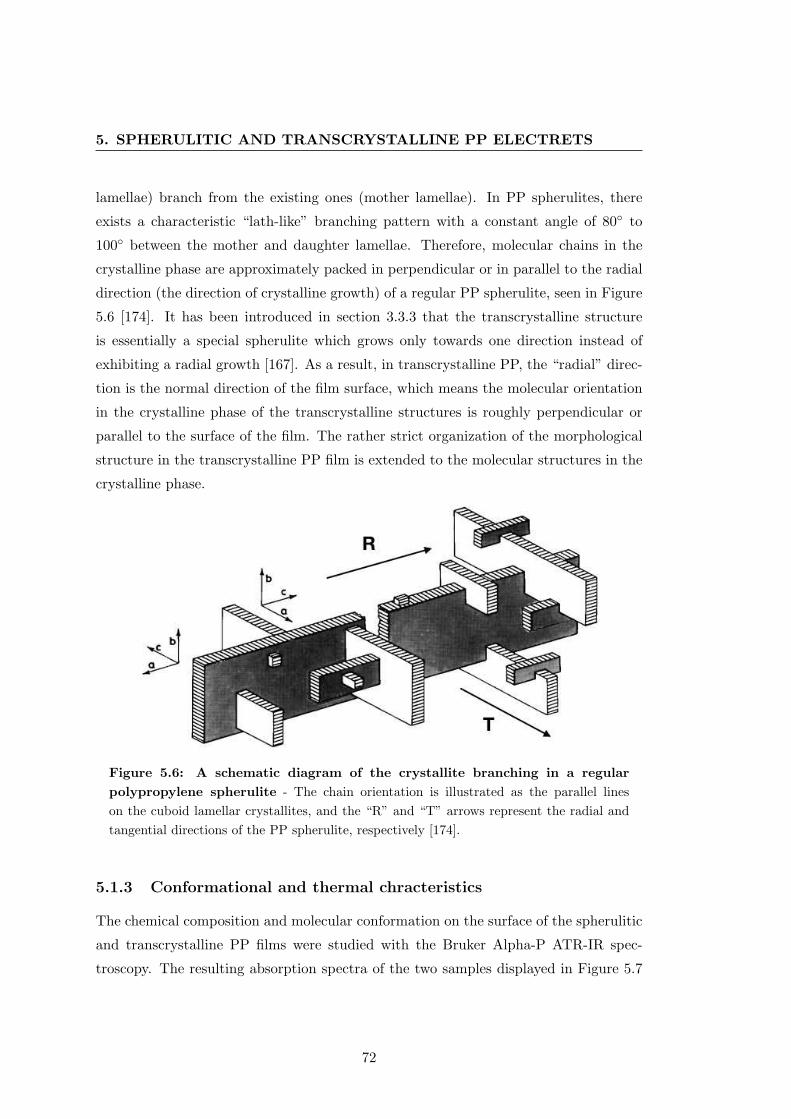
5. SPHERULITIC AND TRANSCRYSTALLINE PP ELECTRETS
lamellae) branch from the existing ones (mother lamellae). In PP spherulites, there
exists a characteristic “lath-like” branching pattern with a constant angle of 80◦ to
100◦ between the mother and daughter lamellae. Therefore, molecular chains in the
crystalline phase are approximately packed in perpendicular or in parallel to the radial
direction (the direction of crystalline growth) of a regular PP spherulite, seen in Figure
5.6 [174]. It has been introduced in section 3.3.3 that the transcrystalline structure
is essentially a special spherulite which grows only towards one direction instead of
exhibiting a radial growth [167]. As a result, in transcrystalline PP, the “radial” direc-
tion is the normal direction of the film surface, which means the molecular orientation
in the crystalline phase of the transcrystalline structures is roughly perpendicular or
parallel to the surface of the film. The rather strict organization of the morphological
structure in the transcrystalline PP film is extended to the molecular structures in the
crystalline phase.
Figure 5.6: A schematic diagram of the crystallite branching in a regular
polypropylene spherulite - The chain orientation is illustrated as the parallel lines
on the cuboid lamellar crystallites, and the “R” and “T” arrows represent the radial and
tangential directions of the PP spherulite, respectively [174].
5.1.3 Conformational and thermal chracteristics
The chemical composition and molecular conformation on the surface of the spherulitic
and transcrystalline PP films were studied with the Bruker Alpha-P ATR-IR spec-
troscopy. The resulting absorption spectra of the two samples displayed in Figure 5.7
72

5.1 Spherulitic and transcrystalline PP
3 5 0 0 3 0 0 0 2 5 0 0 2 0 0 0 1 5 0 0 1 0 0 0 5 0 00 . 0 0
0 . 0 4
0 . 0 8
0 . 1 2
0 . 1 6
0 . 2 0
0 . 2 4 t r a n s c r y s t a l l i n e s p h e r u l i t e
Abso
rbanc
e
W a v e n u m b e r ( c m - 1 )Figure 5.7: Attenuated-total-reflection infrared (ATR-IR) spectra of the
spherulitic and transcrystalline polypropylene films - The two spectra overlap with
each other, indicating no chemical compositional and molecular conformational differences
between them.
Table 5.1: The melting temperatures (Tm) and degree of crystallinity (Xc) extracted
from the DSC results of the spherulitic and transcrystalline PP samples
Crystalline type Tm range Tm peak Xc
spherulite 158-168 ◦C 164 ◦C 46.5 %
transcrystalline 159-169 ◦C 165 ◦C 44.1 %
overlap with each other, which are also consistent with the spectrum of standard isotac-
tic PP in the FTIR software database. It indicates that no detectable foreign chemicals
have been introduced to the PP surfaces during the crystallisation of the spherulite
and the transcrystalline structure. The difference between the two samples lies in their
crystalline structures instead of their chemical compositions. In addition, the regularity
bands of the spherulitic and transcrystalline PP between 700 and 1400 cm−1 that reflect
the length of the molecular helices in the isotactic PP are also identical. The molecular
conformation does not differ when the crystalline structure varies in the samples.
The curves in Figure 5.8 are obtained with the 214 Polyma DSC from NETZSCH.
5 mg of each spherulitic and transcrystalline PP films was tested in the DSC with a
heating and cooling rate of 5 ◦C/min. The thermal transition peaks of the melting
73

5. SPHERULITIC AND TRANSCRYSTALLINE PP ELECTRETS
0 2 0 4 0 6 0 8 0 1 0 0 1 2 0 1 4 0 1 6 0 1 8 0 2 0 0- 1 . 6
- 1 . 2
- 0 . 8
- 0 . 4
0 . 0
0 . 4
0 . 8
1 . 2
endo
Heat
flow (
mW/m
g)
T e m p e r a t u r e ( o C )
exo
Figure 5.8: Differential scanning calorimetry (DSC) curves of spherulitic and
transcrystalline polypropylene films - The DSC curves exhibit no dramatic variations
on the thermal properties and crystallinity of the spherulitic (solid line) and transcrystalline
(dashed line) PP films
and crystallisation of the two crystalline structures show some slight deviations. The
crystallisation peak of the spherulitic PP film is narrower, but its melting peak is of
the same width as that of the transcrystalline PP film. The melting temperatures (Tm)
of the two samples are extracted from the curves and their values of crystallinity (Xc)
are calculated based on (3.8), which are all listed in Table 5.1. The difference between
their Tm is only 1 ◦C and the variation of their Xc is within the deviation of repeated
measurements on identical PP samples. The thermal properties and crystallinity of PP
are mostly controlled by the thermal history. During the crystallisation, the spherulitic
and transcrystalline PP films experienced the same thermal history. Thus, they show
very similar Tm and Xc but very different orientations of crystalline growth. The
spherulitic and trascrystalline PP samples in this experiment are essentially built with
the same “elementary structures”, which, however, are assembled differently in each
sample.
74

5.2 Characterisation of electret properties
5.2 Characterisation of electret properties
5.2.1 Charging and discharging procedures
The crystalline structures of the spherulitic and transrcystalline PP films have been
confirmed with the PLM. For the investigation of the electret behaviour of the different
crystalline structures in PP, the sample films were charged with a corona triode in air
for 15 seconds at room temperature. The charges were deposited on the nucleating
surface of the PP films and the Al substrate was used as the electrode during charging
and discharging. The corona point with a voltage of ±12 kV was positioned 20 mm
away from the open surface of the PP samples, while the control grid was 7-8 mm above
the sample surface. The voltage of the control grid was set at ±500 V, ±1 kV or ±2
kV to research the influence of the surface charge density on the electret properties of
the PP films with the spherulites and transcrytalline structures.
Immediately after the corona charging, the transcrystalline and spherulitic PP elec-
trets were transferred to the TSD set-up. The temperature of the PP electrets was
increased linearly with a heating rate of 3 ◦C/min, and the surface potential decay
was measured with a non-contact electrostatic voltmeter supplied by TREK (model
314B). The results are presented as surface-potential decay curves versus temperature.
Each of the curves is the averaged result from three to six individual measurements on
identical samples.
5.2.2 Charge storage and transport characteristics
The charge decay behaviours of the spherulitic (solid line) and transcrystalline (dashed
line) PP electrets charged with various grid voltages (VG) are exhibited in Figure 5.9
and 5.10 for the negative and positive surface charges, respectively. It is easily noticed
that the initial surface potential of the spherulitic PP is still far below ±1 kV when
the VG increases above ±1 kV. To be more precise, the positively charged spherulitic
PP films show potential saturation at approximately +700 V in Figure 5.10. The
initial surface potential of the negatively charged samples still increase with the VG,
but the samples are severely undercharged when the VG is set at −1 kV and −2 kV
in Figure 5.9. On the other hand, the initial surface potential of the transcrystalline
PP electrets can roughly meet the value of the set VG up to at least ±2 kV. The
potential-saturation phenomenon in PP electrets with large spherulites was reported
75

5. SPHERULITIC AND TRANSCRYSTALLINE PP ELECTRETS
by Ikezaki and coworkers [155, 161]. However, it does not occur in the PP samples with
the spherulites in smaller size and higher number density.
2 0 4 0 6 0 8 0 1 0 0 1 2 0 1 4 0 1 6 0 1 8 00
- 5 0 0
- 1 0 0 0
- 1 5 0 0
- 2 0 0 0
V G = − 5 0 0 V
V G = − 1 k VV G = − 2 k V
Surfa
ce po
tentia
l (V)
T e m p e r a t u r e ( o C )Figure 5.9: Thermally stimulated discharge (TSD) curves of the negatively
corona charged spherulitic and transcrystalline PP electrets - The samples are
charged with VG= −500 V, −1 kV and −2 kV. The spherulitic PP (solid line) is under-
charged when VG is higher than −500 V, unlike the transcrystalline PP (dashed line).
In most of the experiments, the differently sized spherulites in PP are obtained
by crystallising the melt at different cooling rates or isothermal conditions, hence the
structural effect from the spherulite size is often intertwined with the molecular con-
formational effect from the different thermal history [169]. However, in this case, the
spherulite and transcrsytalline PP samples are prepared with the same temperature
profile as shown in Figure 5.2, and the similarity of their thermal properties and crys-
tallinity is proven by the DSC method (as shown in Table 5.1). The charge saturation
and undercharging in the large PP spherulites appear immediately after the corona
charging, whereas the deposited charges on the surface only start to decay at ca. 50
◦C. Therefore, it is highly likely that the saturation/undercharging phenomenon is a
surface effect of the spherulitic PP films, which might be attributed to the lower density
of surface nuclei and inter-spherulitic boundaries of the large spherulites compared to
that of the transcrystalline PP.
The surface-potential saturation does not occur to the transcrytalline films, which
can offer enough trapping sites to accommodate all the deposited corona charges. How-
76

5.2 Characterisation of electret properties
2 0 4 0 6 0 8 0 1 0 0 1 2 0 1 4 0 1 6 0 1 8 00
+ 5 0 0
+ 1 0 0 0
+ 1 5 0 0
+ 2 0 0 0
V G = + 5 0 0 V
V G = + 1 k VV G = + 2 k V
Surfa
ce po
tentia
l (V)
T e m p e r a t u r e ( o C )Figure 5.10: Thermally stimulated discharge (TSD) curves of the positively
corona charged spherulitic and transcrystalline PP electrets - The samples are
charged with VG= +500 V, +1 kV and +2 kV. The spherulitic PP (solid line) shows
charge saturation at ca. +700 V, but it does not occur in the transcrystalline PP (dashed
line).
ever, among these traps, only a limited amount are sufficiently deep to withstand high
temperatures. Many corona charges, especially when the charge density is high, are
captured in the shallow traps. Therefore, in Figure 5.9 and 5.10, the “cross-over”
phenomenon can be observed on the curves of the negatively and positively charged
transcrystalline films: all three curves of the transcrystalline samples in each Figure in-
tersect at approximately 70 ◦C. The deposited charges tend to populate the deep traps
when the charge density is low, whereas more and more charges are pushed into the
shallow traps with an increasing charge density. In the meantime, the stronger internal
electric field of the deposited charges will give a higher driving force on the charges
and lead to the charges drifting into the bulk of the transcrystalline PP films before
being captured by the nearby deep traps. Similar as other electrets with the cross-over
feature, the bulk traps of the transcrystalline PP may show much lower activation en-
ergy than the surface traps [170, 172, 175]. In addition, the highly ordered crystallite
structures and molecular orientation in the crystalline phase of the transcrystallised
PP films might serve as the charge-transport channels that are able to facilitate the
charge drifting under high electric fields.
When the VG is ±500 V, the charge saturation and undercharging phenomena have
77

5. SPHERULITIC AND TRANSCRYSTALLINE PP ELECTRETS
not taken place in the spherulitic PP yet, and thus samples with either crystalline
structure can be charged to V0= ± 500 V. But the transcrystalline and spherulitic
PP still differ in their electret behaviour: the former exhibits a symmetrical charge
stability for both polarities, whereas the latter has a T1/2 of 97 ◦C for the negative
surface charges and 90 ◦C for the positive. The difference is more obvious when taking
the first-order derivative of the potential decay with respect to temperature (dV/dT ).
The resulting dV/dT curves of both negatively and positively charged spherulitic (solid
line) and transcrystalline (dashed line) PP electrets are plotted with the temperature
in Figure 5.11.
0 2 0 4 0 6 0 8 0 1 0 0 1 2 0 1 4 0 1 6 0 1 8 0 2 0 0
+ 1 0
+ 5
0
- 5
- 1 0 V G = + 5 0 0 V
dV/dT
(V/o C)
T e m p e r a t u r e ( o C )
V G = − 5 0 0 V
Figure 5.11: First-order derivative of the surface potential in respect of tem-
perature (dV/dT ) of the PP electrets with various crystalline structures. - The
transcrystalline PP (dashed line) shows a symmetrical charge stability for different polar-
ities, while the spherulitic PP (solid line) is slightly more stable when charged negatively.
The transcrystallised PP films show the single peak at 84 ◦C on their dV/dT curves
with the surface charges of either polarity in Figure 5.11. The shape of the dV/dT
curves from the spherulitic samples appear to be different for the positive and negative
corona charges, indicating differences in their energetic distributions of electron and
hole traps. The de-trapping behaviour of the negative charges in the spherulitic PP
is more complex than that of the positive charges. It spreads over a broader energy
78
5.2 Characterisation of electret properties
spectrum. The dV/dT curve of the spherulitic electret with a V0 of +500 V displays
one single peak at 85 ◦C, while there are two parts for the trap distribution in the
spherulitic PP charged to −500 V. One part is a peak at 74 ◦C and the other is a
shoulder-like distribution starting from ca. 110 ◦C.
The simple and complex trap distributions of the transcrystalline and spherulitic
structures in the PP films, respectively, correspond to the orientation of their crystalline
structures. The transcrystalline PP has a simpler structure with the crystalline growth
only in the normal direction of the surface, as illustrated in Figures 5.4 and 5.5. The
crystallites and molecules in the crystalline phase are oriented either perpendicular or
parallel to the surface plane. The spherulitic PP samples, on the other hand, have
a typical radial crystalline growth, where the crystalline structures propagate from
the rather scarce surface nuclei in all directions into the film volume. The broad
range of directions of the crystalline growth in the spherulitic PP electrets leads to
the more diverse charge-transport pathways. The reason that only the negative corona
charges are affected by the radial crystalline structure in the spherulitic PP is not well
understood now. However, it implies that there might be some different mechanisms
regarding the positive and negative charge transport in the spherulitic PP electrets.
The electret properties of the transcrystalline and spherulitic PP vary significantly,
which indicates that some polymeric electrets are highly sensitive to their microscopic
crystalline structures and molecular orientations.
79

5. SPHERULITIC AND TRANSCRYSTALLINE PP ELECTRETS
EMPTY PA
GE
80

6
Charge distribution in
transcrystalline PP
6.1 Single- and double-layer transcrystalline PP
6.1.1 Crystallisation of double-layer transcrystalline PP
The method for preparing the single-layer transcrystalline PP films was introduced in
the last chapter 5.1.1. The single-layer structure was obtained by crystallising PP films
from melt between a moulding surface of PTFE and a substrate of Al foil. For the
double-layer transcrystalline structure, the Al foil was replaced with another PTFE
moulding surface: A piece of commercial PP film from Putz Folien with a nomi-
nal thickness of 50 µm and a diameter of 60 mm was placed in a FEP (TeflonTM)
thickness-control template from DuPont of the same thickness. The PP film and the
FEP template were sandwiched between two identical PTFE films (TeflonTM) with a
thickness of 100 µm. The set-up is illustrated with the schematic diagram in Figure
6.1. All films were rinsed with isopropanol and dried with nitrogen before use.
As shown in Figure 6.1, the sandwich structure was heated under pressure to ensure
a good contact between the melt PP and the moulding surfaces of PTFE. The tem-
perature was kept at 210 ◦C for 10 min before being decreased slowly with the profile
in Figure 5.2. The thermal history of the double-layer transcrystalline films was the
same as that of the single-layer films. The transcrystallisation of the PP films proceeds
from the heterogeneous nuclei on the PTFE moulding surfaces on both sides towards
the middle of the film within ca. 30 min. A transcrystalline interface is created in
81
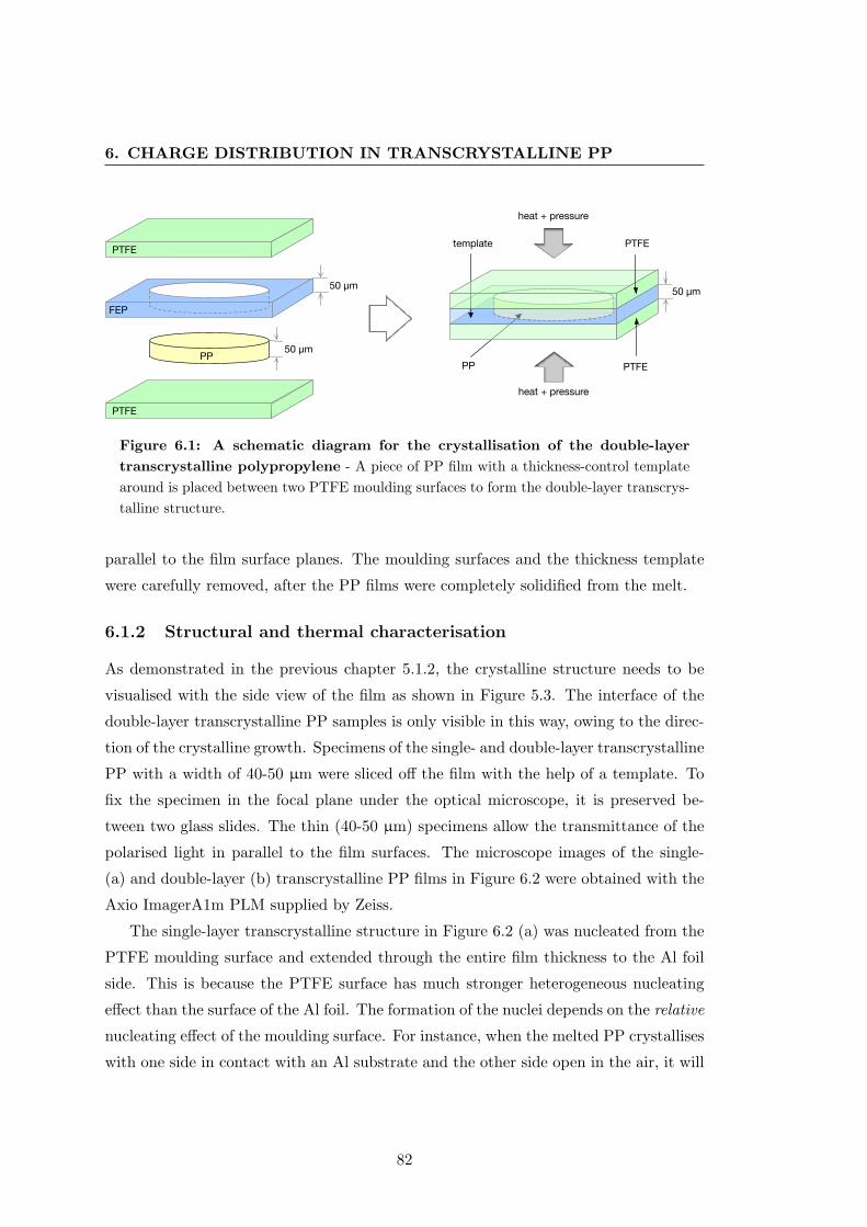
6. CHARGE DISTRIBUTION IN TRANSCRYSTALLINE PP
heat + pressure
heat + pressure
50 µm
PTFE
PTFEPP
templatePTFE
PTFE
FEP
PP 50 µm
50 µm
Figure 6.1: A schematic diagram for the crystallisation of the double-layer
transcrystalline polypropylene - A piece of PP film with a thickness-control template
around is placed between two PTFE moulding surfaces to form the double-layer transcrys-
talline structure.
parallel to the film surface planes. The moulding surfaces and the thickness template
were carefully removed, after the PP films were completely solidified from the melt.
6.1.2 Structural and thermal characterisation
As demonstrated in the previous chapter 5.1.2, the crystalline structure needs to be
visualised with the side view of the film as shown in Figure 5.3. The interface of the
double-layer transcrystalline PP samples is only visible in this way, owing to the direc-
tion of the crystalline growth. Specimens of the single- and double-layer transcrystalline
PP with a width of 40-50 µm were sliced off the film with the help of a template. To
fix the specimen in the focal plane under the optical microscope, it is preserved be-
tween two glass slides. The thin (40-50 µm) specimens allow the transmittance of the
polarised light in parallel to the film surfaces. The microscope images of the single-
(a) and double-layer (b) transcrystalline PP films in Figure 6.2 were obtained with the
Axio ImagerA1m PLM supplied by Zeiss.
The single-layer transcrystalline structure in Figure 6.2 (a) was nucleated from the
PTFE moulding surface and extended through the entire film thickness to the Al foil
side. This is because the PTFE surface has much stronger heterogeneous nucleating
effect than the surface of the Al foil. The formation of the nuclei depends on the relative
nucleating effect of the moulding surface. For instance, when the melted PP crystallises
with one side in contact with an Al substrate and the other side open in the air, it will
82

6.1 Single- and double-layer transcrystalline PP
result in a PP film with the surface spherulites nucleated from the Al substrate, for its
stronger nucleating effect than the air [168]. If the melted PP film is cooled with both
sides exposed to air, which is the case for most commercially produced PP films, there
will be a thin layer of amorphous structure on both of the surfaces of the PP film [98].
(a)
(b)
Figure 6.2: Polarised light microscopic (PLM) images of the (a) single- and (b)
double-layer transcrystalline PP films - A clear interface is observed in the middle
of the double-layer transcrystalline PP (b) from the side view, which is absent in the
single-layer transcrystalline PP sample (a).
However, the melted PP film sandwiched between two PTFE films is under equal
influence of the surface nucleation on both surfaces. Thus, the crystallisation starts
from both sides simultaneously when it is cooled slowly. The high-concentration surface
83
6. CHARGE DISTRIBUTION IN TRANSCRYSTALLINE PP
nuclei on both surfaces lead to the transcrystallisation of the PP samples, instead of
the spherulite formation. The crystalline structures originate from the surfaces and
propagate in the normal direction to the surface into the bulk of the films, resulting in
the double-layer transcrystalline PP in Figure 6.2 (b).
The interface between the two layers is located precisely in the middle of the film
and appears to be straight in Figure 6.2 (b). It indicates that all the nucleation on
the two surfaces of the double-layer transcrystalline PP films happened simultaneously.
This is because the rate of crystalline growth, which relies on the temperature and
cooling rate, is identical for all surface nuclei in this case. It was discussed in section
3.3.3 that the transcrystalline structure can be understood as a special one-dimensional
surface spherulite with extremely dense nucleating centres. Hence, the interface in the
double-layer transcrystalline PP has the same nature as the boundaries between two
spherulites in Figure 5.4 and 5.5. The interface is essentially the point where two
crystalline structures (transcrystalline or spherulite) originating from different nuclei
meet from opposite sides. In addition, the characteristics within the crystalline phase,
including correlation of the crystallite and molecular orientations to the film surfaces as
illustrated in 5.6 [173, 174], are identical for the single- and double-layer transcrystalline
PP films. The interactions and structures of the crystalline and amorphous phases
remain the same within each layer of the transcrystalline structure in both samples.
The thermal properties of the single- and double-layer transcrystalline PP films
were investigated with the 214 Polyma DSC from NETZSCH. The resulting thermal
transition curves are plotted in Figure 6.3. For each measurement, 5 mg of a PP sample
are heated and cooled with a rate of 5 ◦C/min. It is obvious from the DSC result that
the number of the crystalline layers in the single- and double-layer transcrystalline
films does not have measurable impact on their thermal properties. The parameters
of the two thermal transitions, i.e. the melting temperatures (Tm), crystallisation
temperatures (Tc), and degree of crystallinity (Xc) are extracted and listed in Table
6.1. There is no pronounced difference in the thermal properties and crystallinity of
the two different PP samples. It proves that their crystallite structure and interaction
at the crystalline-amorphous interface are the same, as mentioned earlier with the
theoretical prediction [173, 174]. Different Tms are normally observed in the PP films
with different spherulite sizes. However, the films are often produced with different
thermal histories, e.g. by means of isothermal crystallisation at different temperatures
84

6.2 Interfacial charge distribution
0 2 0 4 0 6 0 8 0 1 0 0 1 2 0 1 4 0 1 6 0 1 8 0 2 0 0- 1 . 2
- 0 . 8
- 0 . 4
0 . 0
0 . 4
0 . 8
1 . 2
Heat
flow (
mW/m
g)
T e m p e r a t u r e ( o C )
endo
exo
Figure 6.3: Differential scanning calorimetry (DSC) curves of the single- and
double-layer transcrystalline polypropylene films - No discernible difference between
the single- (dashed line) and double-layer (solid line) transcrystalline PP can be observed
in terms of the thermal transitions and crystallinity.
Table 6.1: The melting temperatures (Tm), crystallisation temperature Tc and degree of
crystallinity (Xc) extracted from the DSC results of the single- and double-layer transcrys-
talline PP samples
Transcrystalline type Tm Tc Xc
single-layer 159-169 ◦C 111-125 ◦C 44.1 %
double-layer 158-168 ◦C 112-125 ◦C 45.6 %
or cooling rates. Their crystalline lamellar structures are influenced by the difference in
the temperature profiles during crystallisation, which does not occur in this experiment.
The characteristic difference between the single- and double-layer transcrystalline PP
films is simply the absence and presence of the transcrystalline interface, respectively.
6.2 Interfacial charge distribution
6.2.1 Charge distribution after corona discharge
For the charging and electrical measurements, the PP samples were metallised on one
side with a 120 nm sputtered Al electrode. The corona needle positioned 20 mm above
the free sample surface was supplied with a voltage of ±12 kV to ionise the ambient air.
85

6. CHARGE DISTRIBUTION IN TRANSCRYSTALLINE PP
The control grid with a voltage (VG) of ±2 kV was placed 7-8 mm above the sample
surface to control the surface potential of the non-metallised surface at the same value
as VG. The corona discharge was carried out at room temperature for 15 seconds.
A partial thermal discharge technique (the same as that in chapter 4 section 4.2.2)
was employed again for activating the charges in the transcrystalline PP electrets. The
samples were partially discharged with the TSD set-up immediately after the corona
charging under a linear heating rate of 3 ◦C/min. When the surface potential reduces to
ca. 0.8 kV and the temperature reaches approximately 60 ◦C, the samples are quenched
to room temperature to freeze the charge distribution at that moment. This method
can mobilise some of the charges to escape from the shallow traps. The mobilised
charges will be either captured in the deep traps or neutralised at the electrodes. In
this way, one can pinpoint the location of the deep traps according to the spatial
charge distribution. Furthermore, this process is equivalent to poling the PP electrets
at elevated temperatures under the electric field of the deposited corona charges and
quenching them to room temperature.
The reference group of the PP transcrystalline electrets were charged with the same
arrangement of the corona set-up, except that the VG was set to ±1 kV. So the ref-
erence samples will carry a similar potential without the follow-up partial discharge.
The charges were deposited onto the surface of the single- and double-layer transcrys-
talline reference films and not activated/mobilised by any thermal stimulations. The
charging was performed at room temperature, and the samples were not subjected to
any thermal discharge. A comparison between the reference group and the partially
thermal-discharged samples may distinguish the effect of thermal activation on the
charges. It can illustrate the charge relocation (escaping from shallow traps and falling
into deep traps) or dissipation (escaping from the shallow traps and being neutralised
at the electrodes) during the thermal discharge.
The charge distributions of the single- and double-layer transcrystalline PP electrets
were measured with the PPS method. For a crystalline structure that particularly grows
along the thickness direction, the charge distribution regarding the thickness direction
of the transcrystalline films is of great interest. It can offer more understanding about
the morphology-related trap distribution in PP electrets. A piece of clean PP film with
a thickness of 25 µm was placed between the corona charged surface of the PP samples
and the rubber electrode of the PPS device in Figure 3.2 to protect the deposited surface
86
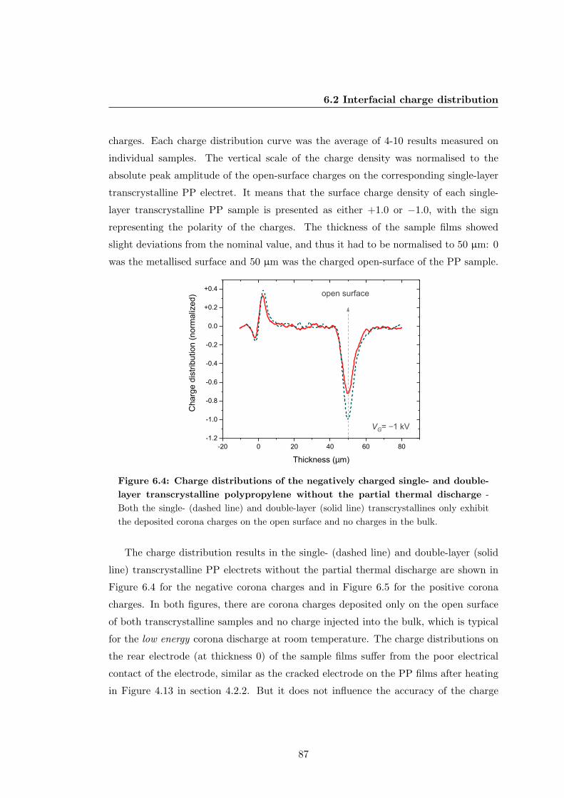
6.2 Interfacial charge distribution
charges. Each charge distribution curve was the average of 4-10 results measured on
individual samples. The vertical scale of the charge density was normalised to the
absolute peak amplitude of the open-surface charges on the corresponding single-layer
transcrystalline PP electret. It means that the surface charge density of each single-
layer transcrystalline PP sample is presented as either +1.0 or −1.0, with the sign
representing the polarity of the charges. The thickness of the sample films showed
slight deviations from the nominal value, and thus it had to be normalised to 50 µm: 0
was the metallised surface and 50 µm was the charged open-surface of the PP sample.
- 2 0 0 2 0 4 0 6 0 8 0- 1 . 2
- 1 . 0
- 0 . 8
- 0 . 6
- 0 . 4
- 0 . 2
0 . 0
+ 0 . 2
+ 0 . 4
V G = − 1 k V
o p e n s u r f a c e
Charg
e distr
ibutio
n (no
rmaliz
ed)
T h i c k n e s s ( µ m )
Figure 6.4: Charge distributions of the negatively charged single- and double-
layer transcrystalline polypropylene without the partial thermal discharge -
Both the single- (dashed line) and double-layer (solid line) transcrystallines only exhibit
the deposited corona charges on the open surface and no charges in the bulk.
The charge distribution results in the single- (dashed line) and double-layer (solid
line) transcrystalline PP electrets without the partial thermal discharge are shown in
Figure 6.4 for the negative corona charges and in Figure 6.5 for the positive corona
charges. In both figures, there are corona charges deposited only on the open surface
of both transcrystalline samples and no charge injected into the bulk, which is typical
for the low energy corona discharge at room temperature. The charge distributions on
the rear electrode (at thickness 0) of the sample films suffer from the poor electrical
contact of the electrode, similar as the cracked electrode on the PP films after heating
in Figure 4.13 in section 4.2.2. But it does not influence the accuracy of the charge
87

6. CHARGE DISTRIBUTION IN TRANSCRYSTALLINE PP
- 2 0 0 2 0 4 0 6 0 8 0- 0 . 4
- 0 . 2
0 . 0
+ 0 . 2
+ 0 . 4
+ 0 . 6
+ 0 . 8
+ 1 . 0
+ 1 . 2
o p e n s u r f a c e
V G = + 1 k VCh
arge d
istribu
tion (
norm
alized
)
T h i c k n e s s ( µ m )
Figure 6.5: Charge distributions of the positively charged single- and double-
layer transcrystalline polypropylene without the partial thermal discharge -
Both the single- (dashed line) and double-layer (solid line) transcrystallines only exhibit
the deposited corona charges on the open surface and no charges in the bulk.
- 2 0 0 2 0 4 0 6 0 8 0- 1 . 0- 0 . 8- 0 . 6- 0 . 4- 0 . 20 . 0
+ 0 . 2+ 0 . 4+ 0 . 6+ 0 . 8 o p e n s u r f a c e
V G = − 2 k V
Charg
e distr
ibutio
n (no
rmaliz
ed)
T h i c k n e s s ( µ m )
Figure 6.6: Charge distributions of the negatively charged single- and double-
layer transcrystalline polypropylene after the partial thermal discharge - There
are heterocharges present at both sides of the crystalline interface in the double-layer
transcrystalline sample (solid line) but not in the single-layer one (dashed line).
88
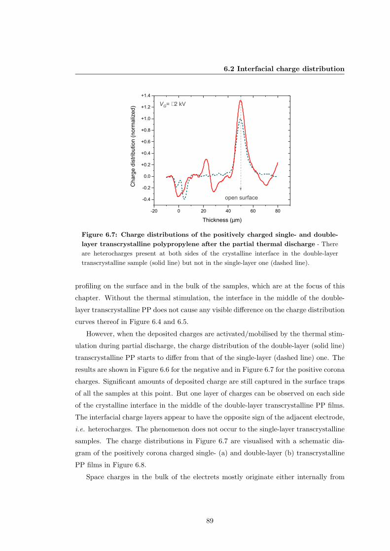
6.2 Interfacial charge distribution
- 2 0 0 2 0 4 0 6 0 8 0- 0 . 4- 0 . 20 . 0
+ 0 . 2+ 0 . 4+ 0 . 6+ 0 . 8+ 1 . 0+ 1 . 2+ 1 . 4
o p e n s u r f a c e
V G = + 2 k V
Charg
e distr
ibutio
n (no
rmaliz
ed)
T h i c k n e s s ( µ m )
Figure 6.7: Charge distributions of the positively charged single- and double-
layer transcrystalline polypropylene after the partial thermal discharge - There
are heterocharges present at both sides of the crystalline interface in the double-layer
transcrystalline sample (solid line) but not in the single-layer one (dashed line).
profiling on the surface and in the bulk of the samples, which are at the focus of this
chapter. Without the thermal stimulation, the interface in the middle of the double-
layer transcrystalline PP does not cause any visible difference on the charge distribution
curves thereof in Figure 6.4 and 6.5.
However, when the deposited charges are activated/mobilised by the thermal stim-
ulation during partial discharge, the charge distribution of the double-layer (solid line)
transcrystalline PP starts to differ from that of the single-layer (dashed line) one. The
results are shown in Figure 6.6 for the negative and in Figure 6.7 for the positive corona
charges. Significant amounts of deposited charge are still captured in the surface traps
of all the samples at this point. But one layer of charges can be observed on each side
of the crystalline interface in the middle of the double-layer transcrystalline PP films.
The interfacial charge layers appear to have the opposite sign of the adjacent electrode,
i.e. heterocharges. The phenomenon does not occur to the single-layer transcrystalline
samples. The charge distributions in Figure 6.7 are visualised with a schematic dia-
gram of the positively corona charged single- (a) and double-layer (b) transcrystalline
PP films in Figure 6.8.
Space charges in the bulk of the electrets mostly originate either internally from
89

6. CHARGE DISTRIBUTION IN TRANSCRYSTALLINE PP
+ + + + + + + + + + +
− − − − − − − − − − − − − − − − − − − − −
− − − − − − − − − − −
+ + + + + + + + + + + + + + + + + + + + +
(a)
(b)
− − − − − − − − − − − − − − − − − − − − −
+ + + + + + + + + + + + + + + + + + + + +
Figure 6.8: An example schematic diagram of the charge distributions after the
partial discharge in the single- and double-layer transcrystalline polypropylene
films - There are deposited corona charges on the open surface and compensation charges
on the rear electrode of the single-layer transcrystalline PP (a), while there additionally
are interfacial heterocharges in the double-layer transcrystalline sample (b).
the intrinsic charge carriers or externally from the charge injection from the adjacent
electrode. The corona needle can be viewed as a distanced electrode that is a source
with the unlimited charge supply. In this case of heterocharges at the interface of the
double-layer transcrystalline PP, the external injection is very unlikely to be the reason.
The interfacial charges with the same polarity of the electrode charges or the surface
charges is located on the other side geometrically. Hence, these charges are most likely
to be intrinsic charges at the interface that are thermally activated and poled by the
deposited charges during the partial discharge, and eventually captured by the traps
on each side of the interface. The origin of the interfacial charges will be investigated
in the following section. Nevertheless, the charges are not completely neutralised by
opposite charges on the surface and electrode or scattered within the transcrystalline
layers. They are trapped at the interface at 60 ◦C instead, where the surface potential
decays to less than half of the initial value. It indicates there are deep traps located
near the crystalline interface that can withstand a temperature of 60 ◦C. Thus, the
crystalline interfaces might be more significant than the transcrystalline structure per
se in terms of charge storage at high temperatures. In addition, the ordered crystallite
and molecules in the crystalline phase within the transcrystalline layers (illustrated in
90

6.2 Interfacial charge distribution
Figure 5.6) may act as the quick transporting channels for charges. Once the charges
escape the deep surface or interface traps, they might move swiftly along the internal
electric field without the pronounced re-trapping within the transcrystalline layers.
6.2.2 Charge distribution after thermal poling
To examine the origin of the interfacial charges in the double-layer transcrystalline PP
electrets, a special thermal poling technique was employed. The schematic diagram of
the set-up is illustrated in Figure 6.9. Two PTFE films supplied by DuPont were used
to block any possible charge injection from the electrodes. The films with a nominal
thickness of 50 µm were inserted between the surface of the transcrystalline samples
and the poling electrode. The excellent electret property and high electrical breakdown
strength of the PTFE can prevent the charge injection from the upper copper electrode
or the bottom grounded electrode that is also the heating plate. For recreating the
poling condition in the last section, the thermal poling was carried out at 60 ◦C for 5
min under a poling electric field (Ep) of ±4×10⁷ V/m that is equivalent to a surface
potential of ±2 kV on a 50 µm film. The positive sign of the electric field is defined as
from the open surface to the rear electrode of the PP film. The as-received PP films
without the transcrystallisation were also charged and examined in the same way as a
reference.
Even the PTFE films can easily withstand a thermal poling of 60 ◦C for 5 min
under ±4×10⁷ V/m without any charge penetrating. The blocking layers of PTFE
films were still measured with the PPS method immediately after the poling for ver-
ification: no charge can be observed in the bulk of the PTFE. It indicates no sign of
the charge injection. The single- and double-layer transcrystalline PP samples were
carefully transferred from the charging set-up to the PPS measurements. Their charge
distributions were examined with the same techniques described in the last section.
The signal of charge density were also normalised by the absolute peak amplitude of
the corresponding single-layer transcrystalline sample in each charging polarity. The
thickness of the sample films had to be normalised to 50 µm for the final charge dis-
tribution results to eliminate the slight variation in the nominal value. The results are
shown in Figure 6.10 and 6.11 for the transcrystalline samples charged with a negative
and positive potential on the upper copper electrode, respectively.
91

6. CHARGE DISTRIBUTION IN TRANSCRYSTALLINE PP
PTFE
PTFE
PP
copper disk
heating
±6 kV
Figure 6.9: A schematic diagram of the special thermal poling method with
the blocking layers for preventing charge injection - The thermal poling was carried
out at 60 ◦C for 5 min with Ep= ±4×10⁷ V/m
- 2 0 0 2 0 4 0 6 0 8 0- 1 . 0- 0 . 8- 0 . 6- 0 . 4- 0 . 20 . 0
+ 0 . 2+ 0 . 4+ 0 . 6+ 0 . 8+ 1 . 0+ 1 . 2
E p = − 4 × 1 0 7 V / m
o p e n s u r f a c e
Charg
e distr
ibutio
n (no
rmaliz
ed)
T h i c k n e s s ( µ m )
Figure 6.10: Charge distributions of the single- and double-layer transcrys-
talline polypropylene charged with a negative potential on the upper copper
electrode - Heterocharges appear on the surface of the single-layer transcrystalline PP
(dashed line) and on the surface and interface of the double-layer sample (solid line).
92

6.2 Interfacial charge distribution
- 2 0 0 2 0 4 0 6 0 8 0- 1 . 2- 1 . 0- 0 . 8- 0 . 6- 0 . 4- 0 . 20 . 0
+ 0 . 2+ 0 . 4+ 0 . 6+ 0 . 8+ 1 . 0
o p e n s u r f a c e
E p = + 4 × 1 0 7 V / m
Charg
e distr
ibutio
n (no
rmaliz
ed)
T h i c k n e s s ( µ m )
Figure 6.11: Charge distributions of the single- and double-layer transcrys-
talline polypropylene charged with a positive potential on the upper copper
electrode - Heterocharges appear on the surface of the single-layer transcrystalline PP
(dashed line) and on the surface and interface of the double-layer sample (solid line).
There are surface charges on all the PP electrets in Figure 6.10 and 6.11. The
polarity of the surface charges is in the opposite correlation with the adjacent electrode
as that of the surface charges on the samples in Figure 6.6 and 6.7, that is the surface
charges in Figure 6.10 and 6.11 are heterocharges. However, the same heterocharge
layers are present on both sides of the middle interface in the double-layer transcrys-
talline films in both cases of thermal poling (charging with the PTFE injection-blocking
layers) and corona poling (thermally stimulated partial discharge). The charge distri-
butions in Figure 6.11 are illustrated with the schematic diagrams in Figure 6.12 for
both transcrytalline samples.
Solely heterocharges are observed in the single- and double-layer transcrystalline
samples in Figure 6.10 and 6.11, and the blocking layers of PTFE can effectively elimi-
nate the possibility of the external charge injection from the thermal poling. Therefore,
it can be concluded that the surface and interfacial charges are most likely to be in-
trinsic charges. They were perhaps initially masked by the neighbouring charges of the
opposite sign and later separated by applying electric field at elevated temperature.
The process is similar to the charge carrier separation in the photoelectrets.
The phenomenon of the intrinsic charge carrier separation under thermal poling
93

6. CHARGE DISTRIBUTION IN TRANSCRYSTALLINE PP
+ + + + + + + + + + +
− − − − − − − − − − − − − − − − − − − − −
− − − − − − − − − − −
+ + + + + + + + + + + + + + + + + + + + +
(b)
− − − − − − − − − − − − − − − − − − − − −
+ + + + + + + + + + + + + + + + + + + + +
(a)
Figure 6.12: An example schematic diagram of the charge distributions in the
thermally poled single- and double-layer transcrystalline polypropylene films
with the positive voltage on the upper electrode - There are heterocharges on the
surface of both single- (a) and double-layer (b) transcrystalline and at the interface of the
latter.
was not observed in the reference as-received PP charged with the same injection-
blocking technique. Thus, the heterocharges present in the single- and double-layer
transcrystalline PP films might be introduced to the samples in the transcrystallisation
process. They might be carried by the impurities or created by the triboelectrification
between the PTFE moulding surface and the PP films. The charges later gain enough
activation energy from the thermal stimulations to escape from the original shallow
traps and to drift under the electric field. Eventually they are captured in the deep
traps either at the interface or on the surface.
There are no charges detected within the transcrystalline layers regardless of the
single- or double-layer composition and the charging methods. This evidently shows
that the transcrystalline interfaces (surface included) can create traps of higher acti-
vation energy in comparison with the transcrystalline structure per se. The crystalline
interface can provide a great disruption on the energy bands with its significant struc-
tural discontinuity. Additionally, when the polymers crystallise from the nucleating
centres, the impurities are pushed further and accumulate at the interfaces, as the
crystalline structure is expanding [138]. These impurities, including the chain ends,
side groups and foreign chemicals of additives, may serve as deeper traps and bind
94
6.2 Interfacial charge distribution
charges at higher temperatures.
It is interesting to notice that PP—a non-polar material—can be thermally poled
to form two layers of opposite charges at a distance merely in the micrometer range.
The two charge layers of opposite polarities separated by the crystalline interface in the
middle of the double-layer transcrystalline PP films, to a certain extent, can be seen
as the “micrometer-scale dipoles”. By introducing voids into the PP films, the cellular
PP ferroelectrets were invented as an alternative for the traditional ferroelectrics with
intrinsic molecular dipoles. By manipulating the crystalline structures of the PP films,
a layer of micrometer-scale “dipoles” can be built in the middle of the double-layer
transcrystalline PP. The PP material, as one of the most common and simple polymer
materials, still has much potential to offer to the modern world of the smart functional
materials.
95

6. CHARGE DISTRIBUTION IN TRANSCRYSTALLINE PP
EMPTY PA
GE
96

7
Conclusion and outlook
7.1 Conclusions
The influence of chemical surface modifications and crystalline reconstructions on the
electret properties of PP films was investigated. The thermal charge stability and
the charge distribution in the thickness direction were discussed. The molecular and
structural changes from different chemical and crystallisation treatments were studied
with infrared spectroscopy, microscopes, and thermal analysis. The results can provide
an insight about the charge storage and transport processes, as well as the information
of traps associated with various chemical and morphological properties.
The H3PO4-induced surface modification was able to increase the thermal stability
of the PP electrets charged to −500 V and +500 V by 47 ◦C and 38 ◦C in their half-
value temperature (T1/2), respectively. However, the enhancement shows a dependence
on the initial surface potential of the PP films and decreases dramatically as it reaches
±3 kV. This phenomenon was explained with the limited amount of newly-formed
deep traps per unit modified open-surface area. The excess deposited charges might
be forced to settle in the shallow intrinsic traps of the PP electrets when the surface
charge density becomes significantly high (±1.2×10⁻³ C·m−2). At this point, more
intrinsic traps may dominate the charge capture, leading to the early charge decay at
low temperatures.
The foreign phosphorus- and oxygen-containing structures, responsible for the deep-
trap formation on the chemically modified PP surfaces, exhibit a higher activation
energy to the negative charges than to the positive charges. These negative-charge
97

7. CONCLUSION AND OUTLOOK
preferential structures result in the asymmetrical surface-charge stability for different
polarities in the H3PO4-modified PP electrets. Such asymmetry in the charge polarity
does not appear in the non-treated PP. The modification with H3PO4 may be employed
to optimise the performance of devices with the non-woven PP fabric filters and PP
ferroelectrets.
The spherulite or transcrystalline structure can be formed in the PP film when it is
crystallised from melt in contact with a smooth or rough moulding surface, respectively.
The difference in the crystalline structure shows its influence on the electret behaviour
of the PP films. The spherulitic PP charged to ±500 V shows asymmetrical charge
stability: the negative surface charges are slightly more stable with a broader double-
peak trap distribution extending to higher temperatures, while the positive charges
decay faster with a less complex single-peak trap distribution. In addition, surface-
potential saturation and undercharging phenomena can be observed on the PP electrets
with the spherulites, which, however, do not take place on the transcrystalline PP films
with virtually the same thermal properties and degree of crystallinity.
Although the transcrystalline PP electrets are able to obtain higher surface po-
tentials of ±1 kV and ±2 kV, their surface charges decay faster with a higher initial
potential, exhibiting the cross-over phenomenon. The charge distribution measure-
ments reveal that the surface traps on the transcrystalline PP films are deeper than
the bulk (volume) traps. Hence, when large amounts of charges are deposited on the
surface, a great portion of the charges might be pushed to the shallow traps and decay
at a lower temperature. Moreover, the one-dimensional transcrystalline structure may
facilitate the charge transport under the high internal electric field.
A double-layer transcrystalline structure with a crystalline interface in the middle
can be constructed by crystallising the PP film with rough moulding surfaces on both
sides. A layer of heterocharges can be found on each side of the transcrystalline interface
when the double-layer transcrystalline PP is subjected to a sufficiently high electric field
at elevated temperatures (typically 60 ◦C). The heterocharges are most likely to be the
internal charges introduced during the transcrytallisation. They are later separated
by the thermal poling and captured in deep traps. The charge profiling shows that
these heterocharges are trapped mainly at the interface and surfaces of the PP films.
The experiment indicates the importance of the transcrystalline interface in terms of
creating large energetic interruptions—deep traps.
98

7.2 Outlook
Polymer materials are extremely versatile in terms of their molecular and morpho-
logical forms. This feature can lead to great advantages, or it may pose problems
when it is overlooked. Polymers can be modified and reconstructed easily to fit the
requirements of many applications. Electret properties of many polymer materials are
highly sensitive to even minor changes of their chemical composition and crystalline
structures. Therefore, it was emphasised in the present thesis that the slight variations
during the polymer processing may lead to dramatic impact on the electret properties
of the PP films. With proper chemical treatments on the surface, the charge stability of
PP electrets can be improved. In the meantime, significant changes on the morphology
of PP films can happen when the substrate for their crystallisation is different, resulting
in a strong influence on their electret behaviour.
7.2 Outlook
The H3PO4 modification on the surface of the PP electrets can be applied to the non-
woven PP fabric filters and the tubular-channel PP ferroelectrets for improving their
performance, particularly the thermal stability. In addition, the island structures on
the PP surface introduced by the H3PO4 treatment can be studied with the microscopic
technique of Kelvin probe force microscope (KPFM). The nanoscale probe of the KPFM
might be useful to investigate the charge trapping behaviour specifically on the islands.
By comparing the electret properties of the foreign-chemical island and that of the PP
matrix, the correlation between the trap depth and the chemical composition will be
interpreted in a more direct way.
The same microscopic experiment can be implemented on the surface spherulites
of the PP films to reveal the difference of traps at the spherulitic interface and the
nucleating centres. Furthermore, the one-dimensional crystalline growth in the trans-
crystalline PP might exhibit certain anisotropic electret properties. PP electrets with
large transcrystalline structures can be used for testing the charge transport in direc-
tions that are parallel or perpendicular to the transcrystalline growth, which can bring
more understanding regarding the charge transport mechanism in the crystalline and
amorphous phases of polymer electrets.
99

7. CONCLUSION AND OUTLOOK
EMPTY PA
GE
100

References
[1] D. B. Malpass and E. Band. Introduction to Industrial Polypropylene: Properties, Catalysts,
Processes. Scrivener Publishing LLC, 2012. 1, 3, 4
[2] T. Taniike and M. Terano. Polyolefins: 50 years after Ziegler and Natta I, 257, chapter The
Use of Donors to Increase the Isotacticity of Polypropylene. Springer, Berlin, Heidelberg, 2013.
1
[3] J. A. Brydson. Plastic Materials. Butterworths, London, 5th edition, 1989. 2, 4, 5, 8
[4] D. Feldman. Polymer History. Des. Monomers Polym., 11(1):1–15, 2008. 2, 8
[5] R. B. Seymour and T. Cheng, editors. History of Polyolefins: The World’s Most Widely Used
Polymers. D. Reidel Publishing Company, Holland, 1986. 2
[6] J. Nicolas, S. Mura, D. Brambilla, N. Mackiewicz, and P. Couvreur. Design,
functionalization strategies and biomedical applications of targeted biodegrad-
able/biocompatible polymer-based nanocarriers for drug delivery. Chem. Soc. Rev.,
42:1147–1235, 2013. 3
[7] F. Carpi and E. Smela, editors. Biomedical Applications of Electroactive Polymer Actuators.
John Wiley & Sons, Inc., 2009. 3
[8] H. R. Sailors and J. P. Hogan. History of Polyolefins. J. Macromol. Sci. A, 15(7):1377–
1402, 1981. 3
[9] D. Tripathi. Practical Guide to Polypropylene. Rapra Technology LTD, UK, 2002. 4, 5
[10] J. R. Jambeck, R. Geyer, C. Wilcox, T. R. Siegler, M. Perryman, A. Andrady,
R. Narayan, and K. L. Law. Plastic waste inputs from land into the ocean. Science,
347(6223):768–771, 2015. 5
[11] K. Sudesh and T. Iwata. Sustainability of Biobased and Biodegradable Plastics. Clean
: soil, air, water, 36(5-6):433–442, 2008. 5
[12] Z. Li and B. Du. Polymeric insulation for high-voltage dc extruded cables: challenges
and development directions. IEEE Electr. Insul. Mag., 34(6):30–43, 2018. 5, 41
101

REFERENCES
[13] J. Zha, H. Yan, W. Li, and Z. Dang. Morphology and crystalline-phase-dependent
electrical insulating properties in tailored polypropylene for HVDC cables. Appl.
Phys. Lett., 109(22):222902, 2016. 5, 35, 41, 43
[14] X. Huang, Y. Fan, J. Zhang, and P. Jiang. Polypropylene based thermoplastic poly-
mers for potential recyclable HVDC cable insulation applications. IEEE Trans. Di-
electr. Electr. Insul., 24(3):1446–1456, 2017. 5, 41
[15] T. Andritsch, A. Vaughan, and G. C. Stevens. Novel insulation materials for high
voltage cable systems. IEEE Electr. Insul. Mag., 33(4):27–33, 2017. 6
[16] M. Albertini, A. Bareggi, L. Caimi, L. de Rai, A. Dumont, S. F. Bononi, and G. Pozzati.
Development and high temperature qualification of innovative 320 kV DC cable with
superiorly stable insulation system. In 9th International Conference on Insulated Power
Cables, number A7.3, Versailles, France, 21-25 June 2015. 6
[17] J. van Turnhout, C. van Bochove, and G. van Veldhuizen. Electret Fibres for High
Efficiency Filtration of Polluted Gases. Staub-Reinhalt. Luft, 36(1):36–39, 1976. 6
[18] S. Bauer, R. Gerhard, and G. Sessler. Ferroelectrets: Soft Electroactive Foams for
Transducers. Phys. Today, 57(2):37–43, 2004. 6, 10, 11
[19] G. Sessler, editor. Electrets, 33 of Topics in Applied Physics. Springer Berlin Heidelberg, 2nd
edition, 1987. 6, 7, 15, 16, 17, 18, 19, 20, 21, 23, 27, 28
[20] G. Odian. Principles of Polymerization. Wiley-Interscience, 2004. 6, 33
[21] G. Sessler and J. West. Self Biased Condenser Microphone with High Capacitance.
J. Acoust. Soc. Am, 34(11):1787–1788, 1962. 7
[22] R. Gerhard. Dielectric materials for electro-active (electret) and/or electro-passive
(insulation) applications. In International Conference on Electrical Materials and Power
Equipment (ICEMPE), pages 91–96, Guangzhou, China, 7-10 April 2019. 7
[23] S. Gray. A Letter from Mr. Stephen Gray to Dr. Mortimer, Secr. R. S. Containing a
Farther Account of His Experiments concerning Electricity. Philos. Trans., 37:285–291,
1732. 7
[24] M. Faraday. Experimental researches in electricity. R. and J. E. Taylor, London, 1839-1855. 7
[25] O. Heaviside. Electromagnetic Induction and Its Propagation. Electrization and Elec-
trification. Natural Electrets. The Electrician, pages 230–231, 1885. 7
[26] M. Eguchi. On Dielectric Polarisation. Proc. Phys. Math. Soc. Jpn., 3(1):326–331, 1919. 7,
21
[27] M. Eguchi. Further Researches on Permanently Polarised Dielectric. In Proceedings of
the Physico-Mathematical Society of Japan. 3rd Series, 2, pages 169–176, 1920. 7
[28] M. Eguchi. XX. On the permanent electret. Philos. Mag., 49(289):178–192, 1925. 7
102

REFERENCES
[29] P. Selenyi. Uber die durch Kathodenstrahlung bewirkte electrische Aufladung des
Glases. Z. Tech. Phys., 9:451–454, 1928. 7, 20
[30] P. Selenyi. On the Electrographic Recording of Fast Electrical Phenomena. J. Appl.
Phys., 9(10):637–641, 1938. 7, 20
[31] C. F. Carlson. Electron photography. US Patent, page 2221776A, 1940. 7
[32] L. B. Schein. Electrophotography and Development Physics. Springer-Verlag Berlin Heidelberg,
2nd edition, 1992. 7
[33] J. Van Turnhout. The use of polymers for electrets. J Electrostat., 1(2):147–163, 1975.
7, 13, 26
[34] P. C. A. Hammes and P. P. L. Regtien. An integrated infrared sensor using the
pyroelectric polymer PVDF. Sensor. Actuat. A-Phys., 32(1):396–402, 1992. 9
[35] I. Grabec and M. Platte. A comparison of high-performance acoustic emission trans-
ducers. Sensor. Actuat., 5(4):275–284, 1984. 9
[36] Y. Wada and R. Hayakawa. Piezoelectricity and Pyroelectricity of Polymers. Jpn. J.
Appl. Phys., 15(11):2041–2057, 1976. 9
[37] R. Gerhard. From electrode charges on dielectric elastomers to trapped charges and
electric dipoles in electrets and ferroelectrets: fundamental and applications-relevant
aspects of diversity in electroactive polymers. In Proceedings of SPIE, Electroactive Poly-
mer Actuators and Devices (EAPAD), 9798, page 97980T, Las Vegas, USA, 20-24 March 2016.
9
[38] J. N. Wilson, J. M. Frost, S. K. Wallace, and A. Walsh. Dielectric and ferroic
properties of metal halide perovskites. APL Mater., 7(1):010901, 2019. 10
[39] M. Nakamura and K. Yamashita. Polarization effect on wettability of bioceramic
electrets. IEEE Trans. Dielectr. Electr. Insul., 19(4):1247–1252, 2012. 10
[40] A. Savolainen and K. Kirjavainen. Electrothermomechanical Film. Part I. Design
and Characteristics. J Macromol. Sci. A, 26(2-3):583–591, 1989. 10
[41] X. Qiu, A. Mellinger, M. Wegener, W. Wirges, and R. Gerhard. Barrier Discharges
in Cellular Polypropylene Ferroelectrets: How Do They Influence the Electrome-
chanical Properties? J. Appl. Phys., 101(10):104112, 2007. 10, 11, 20
[42] R. Gerhard. A matter of attraction: Electric charges localised on dielectric polymers
enable electromechanical transduction. In IEEE Conference on Electrical Insulation and
Dielectric Phenomena (CEIDP), pages 1–10, Des Moines, USA, 19-22 October 2014. 12
[43] R. Gerhard, S. Bauer, and X. Qiu. Charge-spring model for predicting the piezoelec-
tric response of dielectric materials: Considering tetragonality extends validity to
ferroelectric crystals. In IEEE Conference on Electrical Insulation and Dielectric Phenomena
(CEIDP), pages 81–84, Toronto, Canada, 16-19 October 2016. 12
103

REFERENCES
[44] G. S. Neugschwandtner, R. Schwodiauer, S. Bauer-Gogonea, S. Bauer, M. Paajanen,
and J. Lekkala. Piezo- and pyroelectricity of a polymer-foam space-charge electret.
J. Appl. Phys., 89(8):4503–4511, 2001. 12
[45] S. Bauer. Polymer electrets in flexible electronics. In IEEE 14th International Symposium
on Electrets (ISE), pages 25–26, Montpellier, France, 28-31 August 2011. 12
[46] O. Voronina, M. Wegener, W. Wirges, R. Gerhard, L. Zirkel, and H. Munstedt.
Physical foaming of fluorinated ethylene-propylene (FEP) copolymers in supercriti-
cal carbon dioxide: single-film fluoropolymer piezoelectrets. Appl. Phys. A, 90(4):615–
618, 2008. 12
[47] R. A. P. Altafim, X. Qiu, W. Wirges, R. Gerhard, R. A. C. Altafim, H. Basso, W. Jen-
ninger, and J. Wagener. Template-based Fluoroethylenepropylene Piezoelectrets
with Tubular Channels for Transducer Applications. J. Appl. Phys., 106(1):014106,
2009. 12
[48] R. A. P. Altafim, R. A. C. Altafim, X. Qiu, S. Raabe, W. Wirges, H. Basso, and
R. Gerhard. Fluoropolymer Piezoelectrets with Tubular Channels: Resonance Be-
havior Controlled by Channel Geometryith Tubular Channels: Resonance Behavior
Controlled By Channel Geometry. Appl. Phys. A, 107:965–970, 2012. 12
[49] J. Van Turnhout, W. J. Hoeneveld, J. C. Adamse, and L. M. Van Rossen. Electret
Filters for High-Efficiency and High-Flow Air Cleaning. IEEE Trans. Ind. Appl., IA-
17(2):240–248, 1981. 13
[50] R. Thakur, D. Das, and A. Das. Electret Air Filters. Sep. Purif. Rev., 42(2):87–129, 2013.
13, 20
[51] B. Gross. Experiments on Electrets. Phys. Rev., 66:26–28, 1944. 15
[52] B. Gross. On Permanent Charges in Solid Dielectrics. II. Surface Charges and Tran-
sient Currents in Carnauba Wax. J. Chem. Phys., 17(10):866–872, 1949. 15
[53] R. Gerson and J. H. Rohrbaugh. Experiments on the Carnauba Wax Electret. J.
Chem. Phys., 23(12):2381–2388, 1955. 16
[54] B. Gross and R. J. de Moraes. Polarization of the Electret. J. Chem. Phys., 37(4):710–
713, 1962. 16, 26, 30
[55] M. M. Perlman. Thermal Currents and the Internal Polarization in Carnauba Wax
Electrets. J. Appl. Phys., 42(7):2645–2652, 1971. 16, 26
[56] J. F. Fowler and H. Frohlich. X-ray induced conductivity in insulating materials.
Proc. Royal Soc. Lond. A, 236(1207):464–480, 1956. 16
[57] A. Miller and E. Abrahams. Impurity Conduction at Low Concentrations. Phys. Rev.,
120:745–755, 1960. 16
104

REFERENCES
[58] N. F. Mott. On The Transition To Metallic Conduction In Semiconductors. Can. J.
Phys., 34(12A):1356–1368, 1956. 16, 18
[59] N.F. Mott. Conduction in glasses containing transition metal ions. J. Non-Cryst.
Solids, 1(1):1 – 17, 1968. 16
[60] E. M. Conwell. Impurity Band Conduction in Germanium and Silicon. Phys. Rev.,
103:51–61, 1956. 16, 18
[61] H. Scher and E. W. Montroll. Anomalous transit-time dispersion in amorphous
solids. Phys. Rev. B, 12:2455–2477, 1975. 16, 28
[62] W.A. Schneider and J.H. Wendorff. Electronic Properties of Polymers and Related Com-
pounds, 63, chapter Polymeric Electrets. Springer, Berlin, Heidelberg, 1985. 16, 18, 19
[63] H. Bauser. Ladungsspeicherung in Elektronenhaftstellen in Organischen Isolatoren.
Kunststoffe, 62:192–196, 1972. 16, 17, 18, 28, 35, 63
[64] J. van Turnhout. Thermally Stimulated Discharge of Polymer Electrets. Polym. J.,
2(2):173–191, 1971. 17, 26, 28, 30
[65] P. Wurfel. Physics of Solar Cells: From Principles to New Concepts. Wiley-VCH, 2005. 17,
21
[66] H. von Seggern. Detection of Surface and Bulk Traps. J. Appl. Phys., 52(6):4086–4089,
1981. 19, 26, 56
[67] J. Giacometti, S. Fedosov, and M. Costa. Corona Charging of Polymers: Recent
Advances on Constant Current Charging. Braz. J. Phys., 29(2):269–279, 1999. 20, 22, 23
[68] P. Murphy, S. Ribeira, F. Milanez, and R. Moraes. Effect of Penetrating Radiation
on the Production of Persistent Internal Polarization in Electret-Forming Materials.
J. Chem. Phys., 38(10):2400–2404, 1963. 20, 21
[69] R. Gerhard-Multhaupt, G. M. Sessler, J. E. West, K. Holdik, M. Haardt, and
W. Eisenmenger. Investigation of piezoelectricity distributions in poly(vinylidene
fluoride) by means of quartz- or laser-generated pressure pulses. J. Appl. Phys.,
55(7):2769–2775, 1984. 21, 23, 31, 33
[70] T. Yovcheva, I. Avramova, G. Mekishev, and T. Marinova. Corona-Charged
Polypropylene Electrets Analyzed by XPS. J. Electrostat., 65:667–671, 2007. 23, 37,
59
[71] R. Ono, M. Naakazawa, and T. Oda. Charge Storage in Corona-Charged Polypropy-
lene Films Analyzed by LIPP and TSC Methods. IEEE Trans. Ind. Appl., 40(6):1482–
1488, 2004. 23, 62
[72] R. Gerhard-Multhaupt, G. Eberle, Z. Xia, G. Yang, and W. Eisenmenger. Electric-
field profiles in corona- or electron-beam-charged and thermally treated Teflon
PTFE, FEP, and PFA films. In IEEE Conference on Electrical Insulation and Dielectric
Phenomena (CEIDP), pages 61–66, Victoria, Canada, 18-21 October 1992. 23
105

REFERENCES
[73] P. Southgate. Room-temperature Poling and Morphology Changes in Pyroelectric
Polyvinylidene Fluoride. Appl. Phys. Lett., 28(5):250–252, 1976. 23
[74] R. Moreno and B. Gross. Measurement of Potential Buildup and Decay, Surface
Charge Density, and Charging Currents of Corona-charged Polymer Foil Electrets.
J. Appl. Phys., 47(8):3397–3402, 1976. 23
[75] E. Motyl. Charging of polypropylene foils in corona triode system. J. Electrostat.,
30:57–64, 1993. 23
[76] J. D. Brodribb, D. M. Hughes, and T. J. Lewis. Electrets: Charge Storage and Transport
in Dielectrics, chapter The Energy Spectrum of Traps in Insulators by Photon-induced Current
Spectroscopy, pages 177–187. The Electrochemical Society, 1973. 25
[77] A. Mellinger, F. C. Gonzalez, R. Gerhard-Multhaupt, L. F. Santos, and R. M. Faria.
Photostimulated discharge of corona and electron-beam charged electret polymers.
In IEEE 11th International Symposium on Electrets (ISE), pages 7–10, Melbourne, Australia,
1-3 October 2002. 25
[78] A. Mellinger. Dielectric resonance spectroscopy: a versatile tool in the quest for
better piezoelectric polymers. IEEE Trans. Dielectr. Electr. Insul., 10(5):842–861, 2003. 25
[79] A Mellinger, F. C. Gonzalez, and R. Gerhard-Multhaupt. Ultraviolet-induced dis-
charge currents and reduction of the piezoelectric coefficient in cellular polypropy-
lene films. Appl. Phys. Lett., 82(2):254–256, 2003. 25
[80] A. Mellinger, F. C. Gonzalez, and R. Gerhard-Multhaupt. Photostimulated dis-
charge in electret polymers: an alternative approach for investigating deep traps.
IEEE Trans. Dielectr. Electr. Insul., 11(2):218–226, 2004. 25
[81] A. Mellinger, R. Singh, and R. Gerhard-Multhaupt. Fast thermal-pulse mea-
surements of space-charge distributions in electret polymers. Rev. Sci. Instrum.,
76(1):013903, 2005. 25
[82] J. D. Brodribb, D. O’Colmain, and D. M. Hughes. The theory of photon-stimulated
current spectroscopy. J. Appl. Phys. D, 8(7):856–862, 1975. 26
[83] P. Ma, Y. Zhang, S. Hole, F. Zheng, Min Gu, and Z. An. Effect of photoemission from
electrode on photo-stimulated discharge spectra. In 2016 IEEE International Conference
on Dielectrics (ICD), 1, pages 187–190, Montpellier, France, 3-7 July 2016. 26
[84] R. W. Tyler, J. H. Webb, and W. C. York. Measurements of Electrical Polarization
in Thin Dielectric Materials. J. Appl. Phys., 26(1):61–68, 1955. 26, 27
[85] R. A. Creswell and M. M. Perlman. Thermal Currents from Corona Charged Mylar.
J. Appl. Phys., 41(6):2365–2375, 1970. 26
[86] H. von Seggern. Identification of TSC Peaks and Surface-voltage Stability in Teflon
FEP. J. Appl. Phys., 50(4):2817–2821, 1979. 26
106

REFERENCES
[87] L. Kelvin. V. Contact electricity of metals. Philos. Mag., 46(278):82–120, 1898. 26
[88] M. A. Noras. Non-contact surface charge/voltage measurements: capacitive probe-
principle of operation. Technical report, Trek Inc., 190 Walnut Street, Lockport, New York
14094, USA, 2002. 27, 28
[89] M. A. Noras. Non-contact surface charge/voltage measurements: Fieldmeter and
voltmeter methods. Technical report, Trek Inc., 190 Walnut Street, Lockport, New York
14094, USA, 2002. 27
[90] P. Molinie. A Review of Mechanisms and Models Accounting for Surface Potential
Decay. IEEE Trans. Plasma Sci., 40(2):167–176, 2012. 29
[91] J. Simmons, G. Taylor, and M. Tam. Thermally Stimulated Currents in Semiconduc-
tors and Insulators Having Arbitrary Trap Distributions. Phys. Rev. B, 7(8):3714–3719,
1973. 29, 56
[92] P. Watson. Transport and trapping of electrons in polymers. IEEE Trans. Dielectr.
Electr. Insul., 2(5):21–27, 1995. 29
[93] J. Li, F. Zhou, D. Min, S. Li, and R. Xia. The energy distribution of trapped charges
in polymers based on isothermal surface potential decay model. IEEE Trans. Dielectr.
Electr. Insul., 22(3):1723–1732, 2015. 29
[94] W. Shen, H. Mu, G. Zhang, J. Deng, and D. Tu. Identification of electron and hole
trap based on isothermal surface potential decay model. J. Appl. Phys., 113(8):083706,
2013. 29
[95] J. Wang, D. Rychkov, and R. Gerhard. Chemical modification with orthophosphoric
acid enhances surface-charge stability on polypropylene electrets. Appl. Phys. Lett.,
110(19):192901, 2017. 29, 49, 50
[96] F. Johann and E. Soergel. Quantitative measurement of the surface charge density.
Appl. Phys. Lett., 95(23):232906, 2009. 30
[97] R. A. Fletcher. Electrostatic microprobe for determining charge domains on sur-
faces. Rev. Sci. Instrum., 86(11):113702, 2015. 30
[98] D. van Krevelen, editor. Properties of Polymers. Elsevier, 3rd edition, 1997. 30, 43, 83
[99] R. E. Collins. Analysis of spatial distribution of charges and dipoles in electrets by
a transient heating technique. J. Appl. Phys., 47(11):4804–4808, 1976. 31
[100] R. E. Collins. Practical application of the thermal pulsing technique to the study of
electrets. J. Appl. Phys., 51(6):2973–2986, 1980. 31
[101] S. B. Lang and D. K. Das-Gupta. A technique for determining the polarization distri-
bution in thin polymer electrets using periodic heating. Ferroelectrics, 39(1):1249–1252,
1981. 31
107

REFERENCES
[102] P. Bloss and H. Schaefer. Investigations of polarization profiles in multilayer systems
by using the laser intensity modulation method. Rev. Sci. Instrum., 65(5):1541–1550,
1994. 31
[103] G. M. Sessler, J. E. West, D. A. Berkley, and G. Morgenstern. Determination of
Spatial Distribution of Charges in Thin Dielectrics. Phys. Rev. Lett., 38:368–371, 1977.
31
[104] P. Laurenceau, G. Dreyfus, and J. Lewiner. New Principle for the Determination of
Potential Distributions in Dielectrics. Phys. Rev. Lett., 38:46–49, 1977. 31
[105] G. Sessler, J. West, and G. Gerhard. High-Resolution Laser-Pulse Method for Mea-
suring Charge Distribution in Dielectrics. Phys. Rev. Lett, 48(8):563–566, 1982. 31
[106] A. Migliori and J. D. Thompson. A nondestructive acoustic electric field probe. J.
Appl. Phys., 51(1):479–485, 1980. 31
[107] W. Eisenmenger and M. Haardt. Observation of charge compensated polarization
zones in polyvinylindenfluoride (PVDF) films by piezoelectric acoustic step-wave
response. Solid State Commun., 41(12):917 – 920, 1982. 31
[108] R Gerhard-Multhaupt, M Haardt, W Eisenmenger, and G M Sessler. Electric-
field profiles in electron-beam-charged polymer electrets. J. Phys. D: Appl. Phys.,
16(11):2247–2256, 1983. 31, 33
[109] R. Gerhard-Multhaupt. Analysis of pressure-wave methods for the nondestructive
determination of spatial charge or field distributions in dielectrics. Phys. Rev. B,
27:2494–2503, 1983. 32, 33
[110] P. Bloss, M. Steffen, H. Schafer, G. Eberle, and W. Eisenmenger. Polarization and
electric field distribution in thermally poled PVDF and FEP. IEEE Trans. Dielectr.
Electr. Insul., 3(3):417–424, 1996. 32, 33
[111] C. Alquie, G. Dreyfus, and J. Lewiner. Stress-Wave Probing of Electric Field Dis-
tribution in Dielectrics. Phys. Rev. Lett, 47(20):1483–1487, 1981. 33
[112] R. Creswell, M. Perlman, and M. Kabayama. Dielectric Properties of Polymers, chapter
The Electret Properties of a Series of Corona-Charged Substituted Polyolefins, pages 295–312.
Plenum Press, Boston, 1972. 34
[113] H. J. Wintle. Introduction to electrets. J. Acoust. Soc. Am, 53(6):1578–1588, 1973. 34
[114] M. Sato, A. Kumada, and K. Hidaka. First-principles determination of electronic
charge transport properties in polymer dielectrics using a crystalline-based model
system. IEEE Trans. Dielectr. Electr. Insul., 26(4):1204–1210, 2019. 34
[115] Seonwoo Kim, Kuniko Suzuki, Ai Sugie, Hiroyuki Yoshida, Masafumi Yoshida, and
Yuji Suzuki. Effect of end group of amorphous perfluoro-polymer electrets on elec-
tron trapping. Science and Technology of Advanced Materials, 19(1):486–494, 2018. 34
108
REFERENCES
[116] M. Sato, A. Kumada, K. Hidaka, T. Hirano, and F. Sato. Quantum chemical calcu-
lation of hole transport properties in crystalline polyethylene. IEEE Trans. Dielectr.
Electr. Insul., 23(5):3045–3052, 2016. 34
[117] P. de Gennes. Scaling Concepts in Polymer Physics. Cornell Univerisity, New York, 1979. 35
[118] A. Yagishita, H. Yamanouchi, and K. Ikezaki. Charge Trapping Sites in Spherulitic
Polypropylene. Jpn. J. Appl. Phys., 38(4R):2053–2058, 1999. 35, 41, 43
[119] R. Nath and M. Perlman. Effect of Crystallinity on Charge Storage in Polypropylene
and Polyethylene. IEEE Trans. Dielectr. Electr. Insul., 24(3):409–412, 1989. 35, 43
[120] M. Meunier, N. Quirke, and A. Aslanides. Molecular modeling of electron traps in
polymer insulators: Chemical defects and impurities. J. Chem. Phys., 115(6):2876–2881,
2001. 35, 63
[121] D. Rychkov and R. Gerhard. Stabilization of Positive Charge On Polytetrafluo-
roethylene Electret Films Treated with Titanium-Tetrachloride Vapor. Appl. Phys.
Lett., 98(12):122901, 2011. 35, 42
[122] D. Rychkov, R. Altafim, X. Qiu, and R. Gerhard. Treatment with orthophosphoric
acid enhances the thermal stability of the piezoelectricity in low-density polyethylene
ferroelectrets. J. Appl. Phys., 111(12):124105, 2012. 35, 37, 42, 48, 50
[123] S. Haridoss and M. M. Perlman. Chemical modification of near-surface charge trap-
ping in polymers. J. Appl. Phys., 55(5):1332–1338, 1984. 35, 42
[124] M. A. Ramazanov and A. S. Guseinova. Effect of the electrothermopolarization on
the electret properties and the charge state of polyethylene nanocomposites with Cr
and PbCrO4 additives. Surf. Engin. Appl.Electrochem., 49(2):97–100, 2013. 35
[125] B. Chen, W. Tang, C. Zhang, L. Xu, L. Zhu, L. Yang, C. He, J. Chen, L. Liu, T. Zhou,
and Z. Wang. Au nanocomposite enhanced electret film for triboelectric nanogener-
ator. Nano Res., 11(6):3096–3105, 2018. 35
[126] H. von Seggern and J. West. Stabilization of Positive Charge in Fluorinated Ethylene
Propylene Copolymer. J. Appl. Phys., 55(7):2754–2757, 1984. 36
[127] G. Yang. Thermally Stimulated Discharge of Electron-beam- and Corona-charged
Polypropylene Films. J. Phys. D: Appl. Phys., 26(4):690–693, 1993. 36, 43
[128] L. Reimer. Scanning Electron Microscopy: Physics of Image Formation and Microanalysis.
Springer-Verlag Berlin Heidelberg, 2nd edition, 1998. 37
[129] D. Rychkov, A. Kuznetsov, and A. Rychkov. Electret Properties of Polyethylene
and Polytetrafluoroethylene Films with Chemically Modified Surface. IEEE Trans.
Dielectr. Electr. Insul., 18(1):8–14, 2011. 37
[130] B. Stuart. Infrared Spectroscopy: Fundamentals and Applications. Analytical Techniques in the
Science. Wiley, Sydney, 1st edition, 2004. 38, 49
109

REFERENCES
[131] J. D. Menczel and R. B. Prime, editors. Thermal Analysis of Polymers: Fundamentals and
Applications. John Wiley & Sons, Inc., 2009. 39
[132] A. J. Muller and R. M. Michell. Polymer Morphology, chapter Differential Scanning
Calorimetry of Polymers, pages 72–99. John Wiley & Sons, Inc., 2016. 39
[133] B. Wunderlich. Thermal Analysis, pages 417–431. Academic Press, 1st edition, 1990. 39
[134] L. Sawyer, D. T. Grubb, and G. F. Meyers. Polymer Microscopy. Springer, 3rd edition,
2008. 39, 40
[135] H. Awaya. Morphology of different types of isotactic polypropylene spherulites crys-
tallized from melt. Polymer, 29(4):591 – 596, 1988. 40
[136] H. D. Keith and Jr. F. J. Padden. A discussion of spherulitic crystallization and
spherulitic morphology in high polymers. Polymer, 27(9):1463–1471, 1986. 40
[137] D.C. Bassett and R.H. Olley. On the lamellar morphology of isotactic polypropylene
spherulites. Polymer, 25(7):935 – 943, 1984. 40
[138] C. Vasile, editor. Handbook of Polyolefins. CRC Press, 2nd edition, 2000. 40, 41, 94
[139] N. Behrendt, N. Mohmeyer, J. Hillenbrand, M. Klaiber, X. Zhang, G. Sessler,
H. Schmidt, and V. Altstadt. Charge Storage Behavior of Isotropic and Biaxially-
Oriented Polypropylene Films Containing alpha- and beta-Nucleating Agents. J.
Appl. Polym. Sci., 99:650–658, 2006. 41, 43
[140] G. Krause, D. Meurer, and D. Klee. Space Charge Formation Related to the Mor-
phology of Polymers. IEEE Trans. Dielectr. Electr. Insul., 24(3):419–424, 1989. 41
[141] X. Li, Q. Du, J. Kang, and D. Tu. Influence of microstructure on space charges of
polypropylene. J. Polym. Sci. B, 40(4):365–374, 2002. 41
[142] J. Ho and T. R. Jow. High field conduction in biaxially oriented polypropylene at
elevated temperature. IEEE Trans. Dielectr. Electr. Insul., 19(3):990–995, 2012. 41
[143] T. Mizutani, E. Nakane, K. Kaneko, M. Ishioka, and H. Takino. Space charge and
charge transport in polypropylene. In IEEE 12th International Symposium on Electrets
(ISE), pages 475–478, Salvador, Brazil, 11-14 September 2005. 41
[144] K. Ikezaki and D. Fujii. Space Charge Limited Currents in Spherulitic Polypropylene.
In IEEE 7th International Symposium on Electrets (ISE), pages 183–188, Berlin, Germany, 25-27
September 1991. 41, 43
[145] H. Fujii, T. Sakamoto, H. Matsuura, and A. Kishi. Electrical Conduction and Charge
Storage of Thin Polypropylene Films Due to Electron Beam Irradiation. In IEEE Con-
ference on Electrical Insulation and Dielectric Phenomena (CEIDP), pages 624–628, Montreal,
Canada, 14-17 October 2012. 41
110
REFERENCES
[146] D. Rychkov, M. Yablokov, and A. Rychkov. Chemical and physical surface mod-
ification of PTFE films—an approach to produce stable electrets. Appl. Phys. A,
107(3):589–596, 2012. 42
[147] D. Rychkov, A. Rychkov, N. Efimov, A. Malygin, and R. Gerhard. Higher Stabil-
ities of Positive and Negative Charge on Tetrafluoroethylene-hexafluoropropylene
Copolymer (FEP) Electrets Treated with Titanium-tetrachloride Vapor. Appl. Phys.
A, 112(2):283–287, 2013. 42
[148] D. Rychkov, R. Gerhard, V. Ivanov, and A. Rychkov. Enhanced Electret Charge
Stability on Polyethylene Films Treated with Titanium-Tetrachloride Vapor. IEEE
Trans. Dielectr. Electr. Insul., 19(4):1305–1311, 2012. 42
[149] Z. An, M. Zhao, J. Yao, Y. Zhang, and Z. Xia. Improved piezoelectric properties of cel-
lular polypropylene ferroelectrets by chemical modification. Appl. Phys. A, 95(3):801–
806, 2009. 42
[150] Z. An, M. Zhao, J. Yao, Y. Zhang, and Z. Xia. Influence of fluorination on piezoelectric
properties of cellular polypropylene ferroelectrets. J. Phys. D: Appl. Phys., 42(1):015418,
2009. 42
[151] Z. An, J. Yao, M. Mao, Y. Zhang, and Z. Xia. Significantly Improved Charge Stabil-
ity of Cellular Polypropylene Films by Fluorination and Subsequent Annealing. J.
Electrostat., 68:523–527, 2010. 42
[152] Z. An, M. Mao, J. Cang, Y. Zhang, and F. Zheng. Significantly improved piezoelectric
thermal stability of cellular polypropylene films by high pressure fluorination and
post-treatments. J. Appl. Phys., 111(2):024111, 2012. 42
[153] M. Tang, Z. An, Z. Xia, and X. Zhang. Electret properties and chemical modification
of cellular polypropylene films. J. Electrostat., 65:203–208, 2007. 42
[154] R. Joshi, R. Schulze, A. Meyer-Plath, M. Wagner, and J. Friedrich. Selective Surface
Modification of Polypropylene using Underwater Plasma Technique or Underwater
Capillary Discharge. Plasma. Process. Polym,, 6:S218–S222, 2009. 42
[155] K. Oka and K. Ikezaki. Effect of Etching Treatment on Thermally Stimulated Current
in Spherulitic Polypropylene. Jpn. J. Appl. Phys., 31(4):1097–1101, 1992. 42, 76
[156] J. S. Mijovic and J. A. Koutsky. Etching of polymeric surfaces: a review. Polym.-Plast.
Technol. Eng., 9(2):139–179, 1977. 43
[157] E. Sheng, I. Sutherland, D.M. Brewis, and R.J. Heath. Effects of the chromic acid
etching on propylene polymer surfaces. J. Adhesion Sci. Technol., 9(1):47–60, 1995. 43
[158] A. Voss, R. W. Stark, and C. Dietz. Surface versus Volume Properties on the
Nanoscale: Elastomeric Polypropylene. Macromolecules, 47(15):5236–5245, 2014. 43
[159] A. Thyssen, K. Almdal, and E. V. Thomsen. Electret stability related to spherulites
in polypropylene. IEEE Trans. Dielectr. Electr. Insul., 22(5):2858–2863, 2015. 43
111
REFERENCES
[160] A. Baba and K. Ikezaki. Drawing and annealing effects on thermally stimulated
currents in polypropylene films. J. Appl. Phys., 72(5):2057–2059, 1992. 43
[161] N. Saito and K. Ikezaki. Electrical Charging Characteristics of Spherulitic
Polypropylene. Jpn. J. Appl. Phys., 28(3R):418–422, 1989. 43, 76
[162] Z. Xia. Improved Charge Stability in Polymer Electrets Quenched before Charging.
IEEE Trans. Dielectr. Electr. Insul., 25(3):611–615, 1990. 43
[163] T. Hata, K. Ohsaka, T. Yamada, K. Nakamae, N. Shibata, and T. Matsumoto. Tran-
scrystalline Region of Polypropylene: Its Formation, Structure and Mechanical
Properties. J. Adhesion, 45(1-4):125–135, 1994. 44
[164] C. W. Lin, S. Y. Ding, and Y. W. Hwang. Interfacial crystallization of isotactic
polypropylene molded against the copper surface with various surface roughnesses
prepared by an electrochemical process. J. Mater. Sci., 36(20):4943–4948, 2001. 43
[165] C. Wang and C.-R. Liu. Transcrystallization of polypropylene composites: nucleating
ability of fibres. Polymer, 40(2):289 – 298, 1999. 43
[166] E. Jenckel, E. Teege, and W. Hinrichs. Transkristallisation in hochmolekularen Stof-
fen. Kolloid-Z., 129(1):19–24, 1952. 43
[167] H. Schonhorn. Transcrystalline growth at a polymer-metal interface. J. Polym. Sci. B
Polym. Lett., 2(4):465–467, 1964. 44, 72
[168] D. R. Fitchmun and S. Newman. Surface crystallization of polypropylene. J. Polym.
Sci. A-2, 8(9):1545–1564, 1970. 44, 83
[169] X. Zhu, D. Yan, and Y. Fang. In Situ FTIR Spectroscopic Study of the Conformational
Change of Isotactic Polypropylene during the Crystallization Process. J. Phys. Chem.
B, 105(50):12461–12463, 2001. 48, 76
[170] M. Ieda, G. Sawa, and U. Shinohara. A Decay Process of Surface Electric Charges
across Poyethylene Film. Jpn. J. Appl. Phys., 6(6):793–794, 1967. 55, 77
[171] E. A. Baum, T. J. Lewis, and R. Toomer. Decay of electrical charge on polyethylene
films. J. Phys. D: Appl. Phys., 10(4):487–497, 1977. 55
[172] T. J. Sonnonstine and M. M. Perlman. Surface-potential decay in insulators with
field-dependent mobility and injection efficiency. J. Appl. Phys., 46(9):3975–3981, 1975.
55, 57, 64, 77
[173] F. Rodriguez, C. Cohen, C. K. Ober, and L. A. Archer, editors. Principles of Polymer
Systems. Taylor & Francis Books, Inc., 5th edition, 2003. 71, 84
[174] B. Lotz and J. C. Wittmann. The molecular origin of lamellar branching in the α
(monoclinic) form of isotactic polypropylene. J. Polym. Sci. B Polym. Phys., 24(7):1541–
1558, 1986. 72, 84
112

REFERENCES
[175] B. Tabti, M. R. Mekideche, M. C. Plopeanu, L. M. Dumitran, A. Antoniu, and L. Das-
calescu. Factors That Influence the Decay Rate of the Potential at the Surface of
Nonwoven Fabrics After Negative Corona Discharge Deposition. IEEE Trans. Ind.
Appl., 46(4):1586–1592, 2010. 77
113

GLOSSARY
114

Glossary
ε0 electric constant or vacuum permittivity that equals to 8.85×10⁻¹² F·m−1.
e the elementary charge, the absolute value of the electric charge carried by an electron,
which is 1.60× 10⁻¹⁹ C.
k the Boltzmann constant, a constant that relates the average relative kinetic energy
of particles in a gas with its temperature. k = 1.38× 10⁻²³ kg·m2s−2K−1.
ATR-IR attenuated-total-reflection infrared spectroscopy, a method for detecting the chemi-
cal composition of a material surface.
DSC differential scanning calorimetry, a widely used measurement for the thermal prop-
erties of polymers.
FEP tetrafluoroethylene hexafluoropolypropylene copolymer, a fluoropolymer, often with
trademark—TeflonTM FEP, with glass transition temperature of 60 ◦C and melting
point of 290 ◦C.
PLM polarised light microscope, a microscopy method often used for observing the crys-
talline structure in polymers.
PP polypropylene, a plastic material with density of 0.905 g/cm3, melting point of 165◦C and glass transition temperature of −18 ◦C. The polypropylene used in this thesis
is isotactic, which can crystallise into different degrees of crystallinity.
PPS piezoelectrically generated pressure step, a method for profiling the charge distribu-
tions in the electrets.
PTFE polytetrafluoroethylene, commonly known with the trademark—TeflonTM TFE, with
a melting point of 327 ◦C, dielectric strength o f 60 MV/m and dielectric constant
of 2.1 (at 1 MHz).
SEM scanning electron microscope, a method for examining the surface properties of
samples with high resolutions.
TSD thermally stimulated discharge, a measurement for studying electret charge decay
behaviour induced by linear heating.
115

GLOSSARY
V0 initial surface potential of the charged electrets
VC the voltage supplied to the needle of the corona triode apparatus for ionising the
molecules in the vicinity
VG the voltage supplied to the control grid of the corona triode apparatus, which is also
the desired value of the initial surface potential on the electrets
116
List of Figures
1.1 Schematic diagrams of the PP molecules in different tacticities. . . . . . 4
1.2 Chemical structures of polypropylene and the TeflonTM . . . . . . . . . 8
1.3 Six different types of electro-mechanical materials . . . . . . . . . . . . . 9
1.4 A schematic diagram of the charging process in a single void . . . . . . 10
1.5 A schematic illustration of the charge-spring model for elastically het-
erogeneous dielectric materials. . . . . . . . . . . . . . . . . . . . . . . . 12
1.6 A schematic illustration of the fibrous electret filter. . . . . . . . . . . . 13
2.1 The trap-modified energy band model . . . . . . . . . . . . . . . . . . . 18
2.2 A graph of temperature and electric field profiles over time in a typical
thermal charging process . . . . . . . . . . . . . . . . . . . . . . . . . . . 21
2.3 A schematic diagram of the classic corona charging apparatus . . . . . . 22
3.1 A schematic illustration of the open-circuit thermally stimulated dis-
charge (TSD) potential measurement apparatus . . . . . . . . . . . . . . 27
3.2 A schematic set-up of a piezoelectrically generated pressure step (PPS)
method. . . . . . . . . . . . . . . . . . . . . . . . . . . . . . . . . . . . . 32
3.3 Views of the spherulites of polypropylene under polarised light micro-
scope (PLM). . . . . . . . . . . . . . . . . . . . . . . . . . . . . . . . . . 40
3.4 Polarised light microscope (PLM) images of the transcrystalline and
spherulitic polypropylene. . . . . . . . . . . . . . . . . . . . . . . . . . . 44
4.1 An illustration of the chemical treatment on polypropylene surfaces. . . 48
4.2 Attenuated-total-reflection infrared (ATR-IR) spectra of non-treated and
chemically treated polypropylene films. . . . . . . . . . . . . . . . . . . . 49
117

LIST OF FIGURES
4.3 Scanning electron microscope (SEM) images of the non-treated and chem-
ically treated polypropylene surfaces. . . . . . . . . . . . . . . . . . . . . 50
4.4 Differential scanning calorimetry (DSC) curves of the non-treated and
chemically treated PP films . . . . . . . . . . . . . . . . . . . . . . . . . 51
4.5 Thermally stimulated discharge (TSD) curves of the negatively charged
non-treated and chemically treated PP electrets. . . . . . . . . . . . . . 53
4.6 Thermally stimulated discharge (TSD) curves of the positively charged
non-treated and chemically treated PP electrets. . . . . . . . . . . . . . 54
4.7 First-order derivative of surface potential with respect to temperature
(dV/dT ) of the negatively charged non-treated and chemically treated
PP electrets. . . . . . . . . . . . . . . . . . . . . . . . . . . . . . . . . . 57
4.8 First-order derivative of surface potential with respect to temperature
(dV/dT ) of the positively charged non-treated and chemically treated
PP electrets. . . . . . . . . . . . . . . . . . . . . . . . . . . . . . . . . . 58
4.9 Charge distributions of partially discharged non-treated PP electrets
with the negative corona charges. . . . . . . . . . . . . . . . . . . . . . . 60
4.10 Charge distributions of partially discharged non-treated PP electrets
with the positive corona charges. . . . . . . . . . . . . . . . . . . . . . . 60
4.11 Charge distributions of partially discharged chemically treated PP elec-
trets with the negative corona charges. . . . . . . . . . . . . . . . . . . . 61
4.12 Charge distributions of partially discharged chemically treated PP elec-
trets with the positive corona charges. . . . . . . . . . . . . . . . . . . . 61
4.13 Optical microscope images of the evaporated electrode on the PP films
with and without heating . . . . . . . . . . . . . . . . . . . . . . . . . . 64
5.1 A schematic diagram for the crystallisation of the spherulitic and tran-
scrystalline polypropylene . . . . . . . . . . . . . . . . . . . . . . . . . . 67
5.2 The temperature profile for the crystallisation of the spherulitic and
transcrystalline polypropylene . . . . . . . . . . . . . . . . . . . . . . . . 68
5.3 A schematic illustration of the direction for observing the crystalline
structures in polypropylene films . . . . . . . . . . . . . . . . . . . . . . 70
5.4 Polarised light microscopic (PLM) images of the spherulites and the
transcrystalline structures in the polypropylene films . . . . . . . . . . . 70
118

LIST OF FIGURES
5.5 Three-dimensional reconstructions of the spherulitic and transcrystalline
polypropylene films . . . . . . . . . . . . . . . . . . . . . . . . . . . . . . 71
5.6 A schematic diagram of the crystallite branching in a regular polypropy-
lene spherulite . . . . . . . . . . . . . . . . . . . . . . . . . . . . . . . . 72
5.7 Attenuated-total-reflection infrared (ATR-IR) spectra of the spherulitic
and transcrystalline polypropylene films . . . . . . . . . . . . . . . . . . 73
5.8 Differential scanning calorimetry (DSC) curves of spherulitic and tran-
scrystalline polypropylene films . . . . . . . . . . . . . . . . . . . . . . . 74
5.9 Thermally stimulated discharge (TSD) curves of the negatively corona
charged spherulitic and transcrystalline PP electrets . . . . . . . . . . . 76
5.10 Thermally stimulated discharge (TSD) curves of the positively corona
charged spherulitic and transcrystalline PP electrets . . . . . . . . . . . 77
5.11 First-order derivative of the surface potential in respect of temperature
(dV/dT ) of the PP electrets with various crystalline structures. . . . . . 78
6.1 A schematic diagram for the crystallisation of the double-layer transcrys-
talline polypropylene . . . . . . . . . . . . . . . . . . . . . . . . . . . . . 82
6.2 Polarised light microscopic (PLM) images of the (a) single- and (b)
double-layer transcrystalline PP films . . . . . . . . . . . . . . . . . . . 83
6.3 Differential scanning calorimetry (DSC) curves of the single- and double-
layer transcrystalline polypropylene films . . . . . . . . . . . . . . . . . . 85
6.4 Charge distributions of the negatively charged single- and double-layer
transcrystalline polypropylene without the partial thermal discharge . . 87
6.5 Charge distributions of the positively charged single- and double-layer
transcrystalline polypropylene without the partial thermal discharge . . 88
6.6 Charge distributions of the negatively charged single- and double-layer
transcrystalline polypropylene after the partial thermal discharge . . . . 88
6.7 Charge distributions of the positively charged single- and double-layer
transcrystalline polypropylene after the partial thermal discharge . . . . 89
6.8 An example schematic diagram of the charge distributions after the par-
tial discharge in the single- and double-layer transcrystalline polypropy-
lene films . . . . . . . . . . . . . . . . . . . . . . . . . . . . . . . . . . . 90
119

LIST OF FIGURES
6.9 A schematic diagram of the special thermal poling method with the
blocking layers for preventing charge injection . . . . . . . . . . . . . . . 92
6.10 Charge distributions of the single- and double-layer transcrystalline polypropy-
lene charged with a negative potential on the upper copper electrode . . 92
6.11 Charge distributions of the single- and double-layer transcrystalline polypropy-
lene charged with a positive potential on the upper copper electrode . . 93
6.12 An example schematic diagram of the charge distributions in the ther-
mally poled single- and double-layer transcrystalline polypropylene films
with the positive voltage on the upper electrode . . . . . . . . . . . . . . 94
120

List of Tables
4.1 Tm, Tc and Xc of non-treated and chemically treated PP samples . . . . 52
4.2 T1/2 of non-treated and chemically treated PP electrets and their differ-
ences (∆T1/2) . . . . . . . . . . . . . . . . . . . . . . . . . . . . . . . . . 55
5.1 Tm and Xc of spherulitic and transcrystalline PP samples . . . . . . . . 73
6.1 Tm, Tc and Xc of single- and double-layer transcrystalline PP samples . 85
121