EhIIIIIEEEI - Defense Technical Information Center · It. OISTISU 346MsTAEEN o ed RPd Aprvdfo7 ......
45
AD-AOB13 659 BROWN UNIV PROVIDENCE R I DIV OF ENGINEERING FIG 20/6 REMOTE OPTICAL CONTROL AND SWITCHING IN OPTICAL FIBER LtNKS. (U) JAN 8O R V GAUTHIER, A V NURNIKKO F19628-7G-C-0009 UNCLASSIFIED RADC -TR-79-396 RL EhIIIIIEEEI IIEEEEEEIIIIEE -I.E-EI l-I flflflflflfl' 8 .0momommomomU
Transcript of EhIIIIIEEEI - Defense Technical Information Center · It. OISTISU 346MsTAEEN o ed RPd Aprvdfo7 ......

AD-AOB13 659 BROWN UNIV PROVIDENCE R I DIV OF ENGINEERING FIG 20/6REMOTE OPTICAL CONTROL AND SWITCHING IN OPTICAL FIBER LtNKS. (U)JAN 8O R V GAUTHIER, A V NURNIKKO F19628-7G-C-0009
UNCLASSIFIED RADC -TR-79-396 RLEhIIIIIEEEIIIEEEEEEIIIIEE-I.E-EI l-Iflflflflflfl' 8
.0momommomomU

NW.' 12.8 12.5I~
11111 .25 111111112.2_
111111 - i, 1111.6
MICROCOPY RI SOLUIION ILSI CHARTNAHINAI l NAll Of ,IANPARPS 14 A

UNCLASSIFIEDSRcuRITY CLASFICATION OF THIS PAGE (01. Dad0 Ene.i __________________
0"' A.qlREP MIikAIO AE X uosc
GW AC9MM S.. CkASICATAONHINGEAIN
79-346_ _ _ __ _ _ __ _ _ _ __ _ _ __ _ /It. OISTISU 346MsTAEEN o ed RPd
Aprvdfo7 ulcrees;diti4in6niie
OACProjCL EONer:LADOTHN N PIL Ot7 Benr 3edo 78O
Opticdl witchinOptialCAnnlWvgie
W Bandidt Elcr-IicMdlto
*0. RAC (Cndhue a, oa,..aid IIneceeaQ ai Ids~fpOp lacknucotrn BE this Rroec wok-mas ee osieedt ahev ig-ped( 1
witchIng a d m d l toCn i t g a e pt c l c r u t
, s i a l o i e
the. roLt eri.
PERPIONNNSEURIT CLASSIIZCAIIO MARADADESt.P O F E NTN PO E CT~. ASK~aud

ITABLE OF CONTENTS j
I. Introduction .$...... ... ... ... .. ... .... 3
II. LiNbO3 Qhannel Waveguides--Some Considerations .... ........ 7
III. Intensity Modulation At High Frequencies In Channel Waveguides. 11
A. General Background ........ .................... 11
B. Focus f his Research .... .................. .... 19
Directional Coupler With Ti In-diffused Guides ... ...... 22
Balanced Bridge With Ti In-diffused Guides .... ........ 25
Experimental Evaluation ....... .................. 32
IV. Conclusion ....... ......................... .... 41
V. References ....... .......................... .. 42
MCESS(ON for
D T IC O Buff-swim 0ELECTE UfWUNM
E E UIFICTION
APR 28 198
SBT LEDn

-2-
EVALUATION
*
This work has potential impact on RADC programs in guided wave
optical communications for C3 . The switch design allows rapid optical
switching in the GHz regime, an important function for enhancing fiber
optics technology.
/E N RD BENDOWProject Engineer

-3-I. INTRODUCTION
The anticipated needs of future lightwave communications system have
already motivated much developmental activity in integrated optical modulators
and switches. In addition to fast data processing applicationssuch as time-
domain multiplexing, a high speed, low drive power modulator offers an
alternative to direct modulation of the light source. This allows more freedom
in the choice of a light source, and relieves the constraints on analog modula-
tion caused by the highly nonlinear pumping characteristics of semiconductor
injection lasers. Therefore, high speed, low drive power light modulators
and switches are of considerable importance to the future of optical comoanica-
tions.
In general terms, optical modulators and switches are devices that impress
information on an optical frequency carrier by imposing a time-varying alteration
of some detectable property of the wave. The information content is proportional
to the bandwidth of the imposed variation. The most common nonabsorptive
mechanisms for switching and modulation are the electrooptic, magnetooptic
and acoustooptic effects. Each can be electrically induced; however, their
relative weakness requires relatively large electric, magnetic, or acoustic
fields. In bulk devices, these fields of necessity occupy a relatively large
volume. Therefore, the stored field energy is high, and the drive power is
high in proportion. One of the principle advantages of an optical waveguide
modulator over a bulk optical modulator is the substantial reduction of the
volume factor allowed by the confinement of the optical beam to a small cross-
section over an extended length.
Of the available physical mechanisms for optical modulation and switching,
the electrooptic effect has found the most widespread application for a
variety of reasons. The devices considered in this work also operate via an
electroeptic interaction, specifically, the change induced by an electricfield in the index of refraction. We limit our consideration here to a linear
E

-4- i
dependence of the index change on the applied field, i.e. the Pockel's effect.
The linear olectrooptic effect in a crystalline material can be described
by small changes in the size and orientation of the index ellipsoid caused by
the applied field. Although the variation of the index ellipsoid is related
to the applied field through a tensor which reflects particular crystalline
symmetry, a simplified relationship may be found that is useful in estimating
the strength of the linear electrooptic effect. For plane polarized light
propagating perpendicular to a principal plane of the index ellipsoid, the
electrooptic refractive index change may be expressed as An a -n rE/2, where
n and r are linear combinations of the principal refractive indices and electro-
optic coefficients, respectively, and E is the appropriate component of the
applied field. The phase shift of a wave of free space wavelength Ao traveling
a distance & associated with a given index of refraction change is A# w 2uLAnl 0o .
Using values of n and r typical of electrooptic crystals, the E-L product
necessary for a I phase shift of .6328P light is about 20,000 volts. From a
standpoint of energy efficiency, it is desirable to confine the electric field
to as small a cross-sectional volume as possible. Ideally, the electric field
would be applied only in the vicinity of the optical been.
A glance through the literature reveals the constant striving for reduction
of the drive/power of modulators and switches. Integrated optical devices
achieve this goal by confining the light beam in one or both transverse directions
to a dimension on the order of a vacuum wavelength. Microelectronics techniques
allow deposition of electrodes to achieve nearly maximal overlap between the
optical and applied electric fields. The large electric fields required for
a significant electrooptic effect can be maintained across the narrow interaction
region by a very modest voltage. Switches requiring only 2 volts to change the
transmitting state have been reported.
The performance of modulators is often specified in terms of the electrical
drive power P required to produce a given degree of modulation over a band-
width Af. The figure of merit is given as P/Af. The useftlness of this

construct is illustrated by considering the bandwidth-drive power tradeoff
for a specific device configuration. A typical electrooptic lumped element
modulator acts as a capacitive load on the driving ciruit. Its capacitance
C is related to the electrode length L and the effective dielectric constant
of the structure c through C = eCoL. Here, C0 is the capacitance per unit
length when the electrodes are in free space. The bandwidth for such a
device is usually limited by the RC charging time rather than optical transit
time considerations. For a resistance R in parallel with the modulator, the(vR¢CoL)"I . ~ 2/ 2L)weeVi
bandwidth is Af (wRcC L)- The drive power is V 2 )
voltage per unit length needed to produce a given degree of modulation. Band-
width and drive power are simultaneously varied by adjusting the shunt
resistance R. However, there is an unavoidable tradeoff between large band-
width and low drive power. The figure of merit P/Af reflects the intrinsic
energy consumption of the modulator, and is useful as a performance standard
independent of optimization for high speed or low drive power.
Although steady improvement in the drive power per bandwidth figure of
merit has been reported, most integrated optical modulators have been of the
lumped-element type. These devices, when tuned by a shunt resistor to match
a SO ohm generator, have bandwidths on the order of 500 iHz. It is apparent
that new device designs are needed to bring speeds into the multi-gigahertz
range while still maintaining sub-Watt power dissipation. The device configura-
tions proposed to accomplish this and the focus of this report,are the traveling-
wave modulators.
Beyond the charging time limitations in a lumped-element modulator,
there is a constraint on the bandwidth caused by the finite transit time of
the optical signal. One method that can overcome this involves applying the
modulating signal in the form of a co-directional traveling wave. In the ideal
case the optical and modulating waves are synchronous, and the bandwidth becomes
"unlimited" ( limited by external constraints or higher frequency dispersion).

-6-
In cases where phase matching does not occur, the bandwidth is limited by the
rate at which the two waves get out of synchronization. If a given integrated
optical modulator could be operated in either a lumped-element or traveling-
wave configuration, a comparison of the figures of merit would prove the more
efficient device.
As noted above, the band width of a traveling-wave modulator is limited
by the phase mismatch between the light and modulating waves. It can easily
be shown that the 3dB bandwidth of a co-directional traveling wave device in
the absence of complete phase match is Af x 1.4c/(w(r' - n)L), where c is the
'effective' dielectric constant of the electrode structure and n is the optical
index of refraction. The drive power of the device is P = V02/(2Z 0 L
2) =
V02C 0cr/(2LJ where the characteristic impedence of the line Z is expressed
as Z = (crEC0 )l. Comparing the P/Af figures for lumped-element and traveling-
wave modulators of the same dimensions, the result
(P/Af) t.w. / CP/Af) lumped = I 1 I /1.4
indicates that for 1 - R1 < 1.4, the traveling wave configuration is more
efficient. This condition is met for most electrooptic materials. As will
be shown later, the ratio of figures of merit for devices considered in this
work is about 1:3 in favor of the traveling-wave configuration.
Of the few reported investigations into traveling-wave integrated optical
modulators, to our knowledge each has resulted in a phase modulator. From
a viewpoint of future communications applications, these devices are much
less useful than intensity modulators and switches. The impetus of this
work, then, was to investigate intensity modulators and switches compatible
with integrated optical circuits applications. In particular, efforts were
centered on high speed, low drive power devices operating via a traveling
wave electrooptic interaction.

1I. LiNbO$ CNNEL WAVEGUIDES--SOME CONSIDERATIONS
An attractive approach to fabricating an integrated optical modulator
is to form the dielectric waveguides within the surface region of a good
electrooptic material. Then, various surface electrode configurations can
be employed to provide an efficient interaction between the confined optical
and the modulating fields. Lithium Niobate (LiNb03 ) is an excellent electrooptic
crystal, exhibiting a large electrooptic coefficient and low optical losses.
Considerable effort has been expanded to develop waveguides in LiNbO3 by in-
diffusion, out-diffusion, ion implantation and epitaxial growth techniques.
The methods of in-diffusion and out-diffusion have yielded high quality wave-
guides with relatively "easy" fabrication.
Lithium Niobate belongs to the 3m crystallographic point group and is
ferroelectric. The Curie Point is I150"C, the melting point is 12530C. The
relative dielectric constants are 28 along the c-axis and 44 perpendicular
to it; the dielectric constant is nearly frequency-independent in the constant
strain case. LiNbO3 is a uniaxial crystal with an ordinary index of refraction
no = 2.29 and an extraordinary index of refraction ne = 2.20 at the vacuum
wavelength of .6328 um and at room temperature. The crystal is transparent
to light of wavelengths from .4 Um to 3 Um. The strongest electrooptic
effect occurs when the modulating electric field is aligned parallel to the
crystalline c-axis and the light propagates perpendicular to the c-axis. Also,
an electric field applied parallel to the crystalline c-axis causes a change
in the magnitude but not the orientation of the index ellipsoid. Hence, there
is only an index change.
The most prevalent contemporary technique for producing channel optical
waveguides in LiNbO3 is an in-diffusion process in which any one of a variety
of metals may be deposited on the surface of the crystal and thermally in-
diffused to cause a local increase in the index of refraction. The prevalent
diffusants are transition metals and their oxides, particularly Titanium (Ti).
-- . . . .-- --- --- ... ..

.-8-
Well known deposition techniques allow precise control of the metal film
thickness before diffusion and complex waveguide configurations are
fabricated easily by the selective diffusion of the photolithographically
patterned film. Titanium has a short diffusion length, but the refractive
index increase is relatively large. This is advantageous in that the optical
waveguide modes are well guided, allowing sharper directional change at guide
bends and less loss. In addition, the optical energy is confined close to the
crystal surface for efficient electrooptic interaction with surface electrodes.
The small guide dimensions (about 3 Um for a single mode), however, make
photolithographic patterning non-trivial, particularly for larger devices.
An obstacle to waveguide formation in LiNbO3 by metal in-diffusion is
that at the high diffusion temperatures (900 - 1000*C), the substrate loses
loosely bound Li20 through a surface out-diffusion process. This deviation
from stoichiometry at the crystal surface increases the extraordinary index
of refraction. As a result, a planar waveguide due to Li20 out-diffusion is
formed in addition to the waveguide produced by the metal in-diffusion. In
a channel waveguide device, the existance of the background out-diffused planar
guide introduces a leak to the channel-guided energy and cross talk between
adjacent channels.
LiNbO can crystallize in slightly non-stoichioinetric form, (Li 0) (NbO0)3 2 V2 Sl -
where v can range from 0.48 to 0.50. It is observed that the ordinary refractive
index n0 is independent of v. However, in the allowed range the extraordinary
index n increases approximately linearly as v decreases (dn /dv = -1.63).e eThe reduction of the Li20 concentration at the surface caused by out-diffusion
forms a graded-index waveguiding layer. The microscopic origin of this behavior
is not presently understood.
Several investigators have reported techniques to overcome the problem
of Li20 out-diffusion during fabrication of Ti in-diffused waveguides. The
methods include treatment of the LiNbO3 sample by Li 2 0 vapor from a Li 20

source, LiNbO3 powder, or Li2CO3 powder at an appropriate point in the Ti
in-diffusion process. The effect of these methods is to either provide a
high enough surface vapor pressure of i 2 0 from an external source to pre-
vent decomposition of the substrate, or to introduce excess Li20 into the
substrate to compensate for Li20 loss. Each author claims success, however
the reproducibility of these techniques is not established.
Prior to the development of the Ti in-diffusion method, controlled Li20
out-diffusion was a prevalent technique for fabricating planar waveguides in
LiNbO3 . The dielectric and electrooptic properties of the out-diffused
region are identical with those of the bulk crystal. The refractive index
change is small, so the high temperatures(- 1000C) and long times
required to produce an index change comparable to the Ti in-diffusion process
are accompanied by long Li20 vacancy diffusion depths, typically in the hundreds
of micrometers. These deep guides are heavily multimode and the optical
energy is not tightly confined near the surface as is desirable for an efficient
electrooptic interaction. Li20 out-diffused waveguides were quickly supplanted
by the Ti in-diffusion process which gave comparable index changes with
guide depths of a few micrometers. In addition, the in-diffusion process is
easily amendable to photolithographic patterning of channels, and the ability
to control the amount of diffusant adds a critical parameter to tailor the
guid index profile.
A novel adeptation of the Li20 out-diffusion process has been developed
by Lee and Goldberg [1] for channel waveguide formation. The technique
involves masking out-diffusion with a capping layer. A thin layer of Si02
is deposited on the crystal surface and the complement of the waveguide
pattern is formed in the SiO 2 film by photolithographic techniques and etching.
The out-diffusiton is carried out at the standard temperature (-. 9300C) but
only for a very short time (,u 25 minutes). The SiO2 layer caps the Li20
out-flow, so the index change occurs only at the LiNbO3 surfaces exposed by

-lO-
the channels in the SiO 2 . The short diffusion time allows only a rather small
index change, and single mode guides are reported with lateral dimensions up
to 15 Pm. This five-fold increase in guide width over single mode Ti in-
diffused guides significantly eases photolithographic tolerances. As Goldberg
and Lee note, unlike the in-diffusion process, where unwanted out-diffusion
of Li20 can also cause an increase in ne, the use of out-diffusion by itself
for waveguide fabrication avoids the problem of having two competing index-
increasing processes. Finally, it must be noted that the out-diffused guides
do not guide light of the n0 polarization; fortunately this polarization has
an electrooptic coeffient only 1/3 the value of the guided ne polarization.
-11-
II. INTENSITY MO)ILATION AT IIIGH FRETIENCIES IN CIINNEL 'AVE1D5S
a. Ceneral Background
Basic configurations for contemporary planar channel wavepuide modulators,
_ mainly of signle mode type, are shown in figure 1. The first structure, the
directional coupler, is characterized by the periodic transfer of power between
the two guides as the optical signal propagates alonp the structure. The prin-
ciple of the directional coupler is modal interference of the eigenmodes of
the two-guide system. The parallel dielectric waveguides interact via their
evanescent fields thereby forming a loosely coupled system. The propagation
distance required for the maximum optical energy to he transferred from one
guide to the other is the coupling length L. Although the physical length
of the device is fixed, the coupling length may he varied electroortically.
Kogelnik and Schmidt have, however, taken advantage of a phase reversal
technique ("stepped AS reversal") which significantly reduces the need for
predetermined coupling lengths f2].
The Balanced Bridge (Integrated Mach Zehnder Interferometer), as illustrated
in figure lb, also operated by modal interference. Iowever, the nower couplint!
regions and the electroopically tuned modulation region are scrarate. The
optical carrier entering either input part is split equally by the 3dR coupler
into the two branching arms of the interferometer. In the section where
the waveguides are spaced far enough to prevent coupling, a relative phase
shift in a given channel can be obtained by an electrooptically induced
index of refraction change. When the two light beams are recombined at the
second 3db coupler, the relative power between the output channels is controlled
by the induced phase shift. The types of structures used to produce the 3dB
coupling sections include directional couplers, tapered velocity couplers,
and branching waveguides.
The transfer characteristics of the directional coupler and the balanced
bridge are somewhat different, and have been discussed In some detail in the
i,.

12
o . 4. 94 . *
0 . 4 4 . . .
* ... . *000.4
3 -dB 4 .4. .
Coule Coupler* *
* 4 . Figure I

-13-
literature [3].
A major advantage of the balanced bridge modulator/switch over the
directional coupler in high-speed integrated optical devices is the separation
of power coupling and modulation functions. This allows the design for each
to be selected and optimized separately. In addition, the modulation element
is only required to produce a net terminal phase shift. The directional
coupler, on the other hand, is analyzed with the assumption of constant dis-
tributed modulation. The integrating effect of the balanced bridge is more
adaptable in overcoming losses and fabrication errors. A liability, however,
is that the balanced bridge requires series connection of three device sections,
resulting in a long device that may increase losses, may require more directional
changes in the optical guiding, and one that is harder to fabricate due to
complexity and increased electrode contacts.
Integrated electrooptic modulators are naturally compatible with planar
electrode structures. On insulating dielectric materials, the fringing
fields from electrodes deposited on or near the substrate surface penetrate
to a depth comparable to the electrode separation. Optical channel guides
in this vicinity provide an efficient interaction volume for light modulation
via the electrooptic effect. For use at high frequencies, electrooptic
modulators require carefully tailored electrodes to reduce capacitance. However,
contemporary microelectronics fabrication techniques, initially for semiconductor
device processing, are available for fabricating integrated optical circuits.
For devices in which the modulating fields is applied via a traveling-
wave structure, it is desirable to maintain the same compatability with planar
device technology. This suggests the investigation of microwave integrated
circuits, particularly those planar configurations in which all conductors
are located on the same dielectric surface. In addition to being simpler
to fabricate, surface strip transmission lines are relatively insensitive to
dielectric substrate tbickness.

-14-
LiNbO3 as a uniaxial crystal has principal relative dielectric constants
Cxx -yy a 43 and czz a 28, where the z direction is taken along the 'optical'
axis. For surface electrode structures, large relative dielectric constants
mean efficient use of the modulating voltage: most of the electric field energy
resides in the dielectric, where it can interact with the guided optical field.
It is easy to show that in cases where the crystal optical axis is perpendicular
to the strip electrode axis, the anisotropic dielectric can be replaced with
an isotropic dielectric with effective relative dielectric constant ceff U
1/2( xx Czz)
One potentially useful surface strip transmission line form is the
coplanar waveRuide. It consists of a thin conducting strip deposited on the
surface of a dielectric slab with two ground electrodes runninR adjacent
and parallel to the strip on the same surface, as illustrated in figure 2a.
There is no low frequency cutoff because of the quasi-T1 mode of propagation.
The vertical componant of the fringing field in the dielectric reverses
direction twice as the structure is traversed, and the horizontal component
is oppositely directed in the gaps. Both polarity effects are potentially
useful in device applications.
The characteristic impedance Z0 of a coplanar waveguide fabricated on
a dielectric half-plane with relative dielectric constant cr has been calculated
by Wen [4). lie shows that Z is a function of the ratio a/b where 2a is the
width of the center strip and 2b is the edge-to-edge separation of the ground
electrodes. It is assumed that the outer ground electrode edges are far
apart (c Urn ). Using a zeroth order, quasi-static approximation, conformal
mapping yields the capacitance per unit length.
C a ( r + l)c0 2K'(m)/K(m)
where K(m) is the complete elliptic integral of the first kind, K' is the
complete elliptic integral of the second kind, and the arRumentm is given by
... .. .. ..

15
(a)oi Igo
Figure 2

-16-
a * a/b.
Wen accounts for the finite width of the ground electrodes by taking
m (a/b) 2 [l - (,/c)2 ]/l[ - (a)21
For a thin planar electrode structure on the interface of air and dielectric
half planes, the transmission line is treated as being totally immersed in
a dielectric of effective dielectric constant (Cr + 1)/2. The phase velocity
for propagation of a TEM mode through such a medium is
V - Clh( r r 1)/2
= C/[(c C * 1)/211/2 for LiNbO3.xx zzV
For a LiNbO3 substrate, the ratio of C/O ("refractive index") for the
traveling modulation wave is 4.2. The characteristic impedence of the coplanar
waveguide is given by
1 1 K(m)
Cv 2c o(Cr + 1)1/2 Im)
Some analysis of the coplanar waveguide has extended the treatment
beyond the idealized structure. Cases in which the electrode thickness is
not insignificant compared to the gap width and cases where the substrate thick-
ness is not very much greater than the gap width have been investigated. These
studies, however, are largely theoretical rather than design oriented. They
do serve to point out where the simple model weakens and second order effects
must be taken into account. Also, experimental verification of the quasi-static
approximation analysis shows some conflict.
Another potentially useful surface strip transmission line is the dual
of the coplanar waveguide, the parallel strip coplanar line (PSCL), shown in
figure 2b. The two strip electrodes are identical; either can be grounded
and the other conducting. The horizontal component of the electric field is
unidirectional in the gap, but the vertical componant reverses sign between
strips. This feature can he exploited to increase the efficiency of an

-17-
electrooptic interaction.
Again, since the field lines between the conducting and ground strips
are not confined entirely to the substrate, the propagating mode along the
line is not purely transverse (TET), but quasi-TFM. There is no low
frequency cutoff. However, at high frequencies, the ratio of longitudinal to
transverse electric field becomes significant and the propagating mode may
no longer be treated as quasi-TEM. Analysis of this "hybrid mode" is far
more rigorous. The approximation has been shown by experiment to he fairly
good up to X-band frequencies.
The capacitance per unit length of the PSCL is found by a conformal mapping
to be
C a (C r + l)o -mwith m = a/b, where 2a Is the gap width and 2b is the separation of the
outer edges of the electrodes. The phase velocity is the same as that of
the coplanar waveguide, so the characteristic impedence is
0 2/2Ce(C + 1) ' / 2 (i)
o r
It is noteworthy from the point of view of fabrication tolerances to observe
that the characteristic impedance does not depend strongly on the ratio of the
electrode strip width to gap ratio. For a nominally 50 n line on LiNho3 , the
strip width to gap ratio may vary from 1.2 to 2.0 while Z remains within
SO ± 2 n. Therefore, the PSCL can be fairly easily matched to the generetor
impedance.
The PSCL has been tested experimentally by lzutsu et. al. in a phase
modulation configuration [5]. The results support the analysis of the line
characteristics, however several resonances due to input and output disconti-
nuities marred operation at frequencies above 3 Ofz. A novel variant of the

-18-
PSCL was proposed and tested by Izutsu et. al. that showed improved frequency
response of the modulation characteristics. The asymmetric PSCL is illustrated
in figure 2c. The analysis of this novel arrangement has been considered by
us by using a conformal mapping technique. In addition, we have assumed that
the 50 0 line on LiNbO3 should be scalable as long as the aspect ratio (a/b)
is fixed.
• t

-19-
b) Focus of This Research
The present investigation of high-speed integrated optical intensity
modulators and switches has resulted in a number of proposed device designs.
All devices are based on a traveling wave electrooptic interaction. However,
*the designs are naturally grouped according to optical waveguide fabrication
technique and modulation configuration. A prototypical design from each group
will be discussed after a few common considerations are introduced.
Of the few schemes proposed for phase-matched electro-optic interaction
in LiNbO3 , none are amenable to an integrated optical format. In the absence
of phase matching, the modulation bandwidth of a traveling wave device is
inversely proportional to the interaction length
Af 1.4 c/r(/ r - n)Lr
As calculated earlier the drive power is proportional to L2
P a V2 cAE- Co/(2L2)0o
Thus the figure of merit, P/Af, is always improved by lengthening the interac-
tion region at the expense of bandwidth. For this reason, effort has been
made to keep the bandwidth above 3 GHz while the 100% modulation voltage is
assumed to be held at about 7 volts or less. This assures that these results
are not only novel, but potentially useful: the bandwidth and drive power
are compatable with the emerging high-speed GaAs FET technology.
All devices proposed here are planned for a Z-cut LiNbO3 substrate.
This is because initial work anticipated employing the unique electric field
distribution provided by the coplanar waveguide in the cobra configuration.
Since all designs were made with fabrication as the ultimate goal, the initial
purchase of Z-cut substrates was a constraint.
Channel waveguides in Z-cut LiNbO3 can guide two families of normal modes
according to the analysis of Marcatili [6). The small axial field components

-20-
make the light waves essentially TE1 in character, with one family of modes
polarized perpendicular to the substrate surface and one family polarized
parallel. Perpendicular polarization gives rise to extraordinary waves that
respond to the r33 electrooptic coefficient for a z directed modulating field.
Guided light polarized parallel to the surface is an ordinary wave connected
with the electrooptic coefficient r13. Since r33 has a value three times
that of r13 , it is muoh more efficient to modulate the extraordinary wave.
This is fortuitous for out-diffused waveguide, as the extraordinary wave is
the only one that can be guided. For Ti-indiffused waveguides, however, this
is a problem; to guide the extraordinary wave, the Li20 out-diffusion must be
stopped or compensated
In a "Cobra" electrode configuration, the metallization is deposted right
above the optical guiding channel, (see figure 3). This can represent a sig-
nificant source of loss for the perpendicular polarization. The reason is
that the boundary condition for a normal electric field allows substantially
more penetration into a non-perfect conductor than for the tangential component.
Thus, the mode with normal electric field will show more loss due to the pre-
sence of the metal boundary. Kaminow and Stulz [7] suggest isolating metal
electrodes from the dielectric waveguide by a thin delectric buffer layer.
The buffer layer should have as low a refractive index as possible to assure
rapid decay of evanescent light field, and it should have as high a dielectric
constant as possible to minimize voltage drop across the buffer layer. Likely
materials include Al 0 and SiO Kaminow and Stulz report reduced losses2 3 2V
with a 2000A thick layer of A1203 on LiNbO3. Care must be taken, however,
since the recent analyses of this multilayer structure show that instead of
decreasing monotonically with increasing buffer thickness, the optical attenu-
ation actually peaks at non-zero buffer thickness.
- .f

+
LiNbO3
FIGURE 3

-22-
Directional Coupler with Ti in-diffused Guides
The directional coupler using stepped AB reversal, as proposed by
Kogelnik and Schmidt [2), can be achieved in an electrooptic device by reversing
the polarity of the applied electric field in each successive step. A 6-
section device, for example, uses 3 Cobra electrodes meandering back and forth
above the optical channels. The applied field (and consequently the phase
mismatch AS) reverses S times along the structure when the center electrode
is grounded and a single drive voltage is applied to the outer electrodes.
In case of the 6 sections, the unused electrode is spaced far from the other
two.
Such a device could be adapted to a traveling-wave configuration by
replacing the lumped element electrodes with a zig-zagging coplanar waveguide.
The electric field distribution under the coplanar waveguide has a normal com-
ponant that changes polarity between the ground electrodes and the conducting
strip. The Cobra configuration applies a strong normal field in the optical
channel region, and in a manner identical to that of Schmidt and Cross [8] (by
shifting the center conductor above alternate channels in successive sections)
the alternating polarity of AS can be achieved.
It is assumed here that the reported optical properties of the Schmidt
and Cross device are accurate and reproducible, and that by following their
procedure, similar guides could be fabricated. They have produced two
3 Um wide singlemode optical channel waveguides by Ti in-diffusion into Z-cut
LiNbO3 using well documented techniques. In the optical coupling region, the
waveguides are spaced 3 um edge to edge over a length of 10.5 m, which they
found to be 5.8 coupling lenghts. As noted earlier, the most efficient switching
will occur in a device sectioned in the integer closest to its interaction
length in units of coupling length. Here, 6 sections are called for.
.......................... ....
-23-
An upper bound for the required switching voltage, assuming a device
biased into one state, can be estimated from the switching characteristics of
the AsB couplers. It follows that the required phase mismatch is bounded by
AOL * 2w
So for he a 2w An between guides, the index change required for each guide is
An 1 A/21
The electrooptically reduced index change in LiNbO3 from a z directed electric
field is
An = n3r Ez/Z
The electric field fringing in Cobra configuration may be estimated from an
expression derived by Marcuse
Ez a2Vf(/g),
where g is the gap spacing between electrodes. Thus, the switching voltage
is bounded by
V
2n 3rL
To limit current through the coplanar waveguide, it is desirable that the
characteristic impedance be at least 50 fl; the 50 fl value is particularly con-
venient since it matches most sources and test equipment. It can be shown,
using the inversion formulae for elliptic integrals, that the required aspect
ratio (a/b as defined in figure 2a) assuming a very large c, is
a/b = .118
* For a 3 um electrode gap (b - a = 3 um) to match the channel waveguide
separation, the width of the central conducting electrode is approximately
.8 um (a - .4 pm). Calculations support the anticipation that electrodes
narrower than 10 Um become excessively lossy. Therefore, a coplanar waveguide
with 50 A characteristic impedence seems unrealizable for these dimensions.

-24-
However, by allowing a 15 Um wide center conductor and 3 um gaps, the char-
acteristic impedence of the line is only reduced to 25 A, which may be accept-
able for some applications.
Resistive loss in the conductors is expected to be a significant problem
for this modulator configuration. Since the analysis is made assuming constant
magnitude of hB throughout the device, attenuated voltage would reduce the
electrooptic effect so the phase correlation decayed in each section and from
section to section. Perhaps this could be compensated by adjusting the elec-
trode length or placement; however, the effect would have to be well-charac-
terized in advance.
Another potentially deleterious effect is the result of the zigzagging
coplanar waveguide. It is expected that this will give rise to radiation and
frequency dependent reflection. The zig-zag transition must be made fairly
abruptly so that the cascaded AB sections appear contiguous. Perhaps coherent
radiation effects could be avoided with unequal step lengths.
The difficulties notwithstanding, the use of a coplanar waveguide provides
a novel and useful way of introducing traveling wave interaction to the stepped
A8 directional coupler. In particular, the designs considered in this project
work were directed toward the development of coplanar guides up to frequencies
of 10 GHz.

-2S-
Balanced Bridge with Ti In-diffused Guides
The balanced bridge configuration, which was analyzed by Ramasway and
Standley [3J for use as an integrated optical switch, appears well suited
for traveling-wave operations. The lumped-element electrodes in the phase
shifter say be replaced by a microwave integrated transmission line. The
advantage of the balanced bridge over the directional coupler is that the
coupling and modulation functions may be separately optimized. Also, the
modulation transfer function depends only on the integral of the distributed
phase shift. The effect of inevitable fabrication errors and conductor losses
may be compensated for by a d. c. bias voltage.
The balanced bridge incorporates a parallel strip coplanar waveguide
(PSCW) in the modulation section; the 3dB coupling may be provided by dc biased
directional couplers. The use of directional couplers is preferred over "y"
branching waveguides because the optical beam is always guided in the directional
couplers and their directionality is better suited to switching operations. The
PSCS is aligned in the Cobra configuration over one branch arm and a lumped
electrode biasing set covers the other arm. It is expected that symmetry
between the branch arms is critical to achieving low cross-talk. Thus, unlike
the device proposed earlier by Ramaswamy and Standley, the arms branch in a
symmetric geometry and the position and area covered by the metallization is
made as similar as possible.
The PSCW used in the modulating section is designed for a 50 Q character-
istic impedance. The aspect ratio is W/g a 1.6, so the electrodes are each 16
va wide, and are separated by a 10 um gap. The PSCW can modulate only one arm
. or it can be used in a "push-pull" configuration where a Cobra electrode covers
each branch arm and induces opposite pulse shifts in each. For identifical
PSCW's, the push-pull" modulation is twice as efficient. However, that con-
-26-
figuration requires that the PSCW gap width equals the branch arm separation.
If wide branch arm separation is necessary, for example, to achieve good
channel isolation, single arm modulation may be more efficient: halving the
PSCW gap doubles the electric field under either Cobra electrode. Of course,
the strip width is halved also to maintain a constant aspect ratio, so that
care must be taken to prevent conductive losses from becoming excessive. Our
early designs made use of single arm modulation because the channels were
separated for good isolation and because it was thought desirable to keep the
microwave line as far from the dc electrodes as possible to avoid ac coupling.
After the PSCW leaves the interaction region, it can be either terminated in
a matched resistance or coupled back off the substrate.
The z directed electric field under the Cobra electrodes of the PSCW is
given by
E 2V
and the phase change in the branch arm due to the applied modulation voltage
is
2n3rVL.- An, - Xvs2g
The figure of merit is halved for the case where "push-pull" modulations is
used. A device assuming lossless 16 um conducting strips with a 10 VE gap
and an interaction length of 8 mm, has a calculated switching voltage of 7V.
The many advantages of the Ti and indiffusion process have made it the
most widely used technique for channel waveguide fabrication in LiMbO3 . The
depostted metal film may be photolithographically patterned and selectively
diffused into the substrate; the resultant channel waveguides are low loss tightly

II-27-
confining. The small cross section guides keep the optical signal close to
the substrate surface, and the relatively large index difference allows
for fairly strong directional changes. Using the published results of
work at Bell Laboratories as a benchmark, single mode channels for
.6328 us light may be produced by in-diffusing 3 Ur wide Ti strips. Of
course, uniform guides require that the pre-diffused strips be without
variation or flow along the entire length of the channel, typically the
length of the device (10 - 25 mm). The techniques for such ultrafine
fabrication are a science in themselves, and the equipment and technology
are presently available in but a handful of laboratories.
In attempting to circumvent the constraints of available funds and
equipment, alternative waveguide fabrication techniques were reviewed by
us. The capped out-diffusion method of Goldberg and Lee is well suited to
the available facilities at Brown University. They have reported single
mode channel waveguides for .6328 um light having channel widths of
15 urn. The channels are defined by etching openings in the capping SiO2
glass layer, and patterns of such dimensions are within the range of Brown
University's facilities. Therefore, device designs have been pursued based
on the modal properties of Li20 out-diffused channel waveguides.
The cause of the large channel cross section, even for a single mode
guide, is that the out-diffusion process results in a very small change in
the extraordinary refractice index of LiNbO3. The light is only weakly
guided; as can be seen from a simple critical angle argument, even a
small angle bend will cause the guided beam to radiate into the substrate.
Therefore, it is not expected that bends and curved sections may be used
to accomplish directional changes in a device with out-diffused waveguides.
It would be advantageous to use straight line guides that do not bend at
all. For this reason, a three guide coupler has been investigated.

-28-
The three guide coupler is a generalization of the two guide directional
coupler which has already been discussed. As illustrated in figure 4 , the
three guide coupler consists of three parallel coplanar guides spaced closely
enough that the evanescent fields of adjacent guides cause weak coupling. This
structure has so far received far less attention than the directional coupler,
however, its unique properties make it attractive as an effective integrated
optical beam splitter without bends.
An analytic treatment of the modes of a three guide structure has
been published by Iwasaki et.al.[9]. For the case of identical guides
spaced by equal separations, there exists a length 1' after which all
optical power initially in the central guide will be split evenly between
the outer guides. After propagating another length ', the power in the
outer guides has returned to the central guide. This suggests beam splitting
and recombination operations. A three guide coupler section of length '
may have only the center input channel excited, and at the output, the
power is evenly divided between the outer guides, with no power in the
central guide. If the central guide is terminated at the end of the 1'
length section but the outer guides continued, their interaction is negligible
with the result that the single input beam has been equally divided into
two isolated output channels. The lateral power flow is accomplished not
by angle bends in a single guide, but by modal interference in a multiple
straight guide section. For recombination, the treatment of Iwasaki et.al.
shows that for equal intensity in-phase signals entering the outer guides
of an 1' length section, all optical power at the termination will reside
in the central guide. However, for components of equal intensity but T
out of phase entering the outer channels, the light exiting a section of
length 91 is entirely in the outer guides. Termination of the outer guides
of such a section causes the structure to respond to a 0 or w phase in the

-29-
FIGURE 1

-30-
separated inputs by either exiting all power out the central guide or scattering
all light at the 'dead' ends of the outer guides.
By using out-diffusion as the optical waveguide fabrication technique and
two three-guide couplers for power splitting and recombination, a balanced bridge
switch has been designed for fabrication at Brown University's facilities.
As illustrated in figure 5, the input channel leads to the central part of
the three guide coupler. The central guide of the coupler is terminated
after one lateral coupling length 1', and the outer guides continue to
form the non-interacting branch arms of the balanced bridge switch. The
recombination coupler, again of length i', is fed by the branch arms. The
outer channels terminate at the end of the coupler section, with only the
central channel continuing on as the output part of the device. An asymmetric
PSCL applies the traveling-wave modulating field in an efficient push-pull
configuration through the Cobra electrodes, The optical channel wave guides
are IS um wide, and in the three guide coupler sections, the guide edge-to-
edge separation is 6 um. The 50 52 characteristic impedence microwave line
has a 16 um wide conducting strip separated from the ground plane by a 27 um
gap. At both ends, the PSCL dimensions are expanded into contact pads;
however, the aspect ratio is kept constant to avoid changes in the character-
istic impedence.
The voltage to induce a w phase shift between the branch arms is
Vs a wx7g/4n3rL
where L is the interaction length and a push-pull configuration is assumed.

II ! 1 . lii lii 'II I I. ii M
I -31-

-32-
Thus, assuming that the bandwidth Af is limited by phase mismatch, the
figure of merit for this device is
P/Af ' 1.9 )2 2 (/c - n)/(cr L n Zo)
The balanced bridge switch with out-diffused waveguides is not a very
satisfactory switch because in the off-state, the light signal is scattered
indiscriminately out the back of the device rather than remaining guided
but having its location altered to another part. In the off-state, some
light will be scattered back into the output channel, degrading the on-off
contrast. This compromise must be made, however, when constrained to work
with straight-section guides.
Experimental Evaluation
The initial intent of this investigation was to design and fabricate
traveling-wave integrated optical modulators based on the well-studied
and documented Ti In-diffusion process for channel waveguides developed at
Bell Laboratories. Such processing, however, requires sophisticated techniques
and often ultramodern equipment. After much time and effort were invested,
it became apparent that fabricating such devices at Brown University was
not possible due to limited resources.
A first problem is the generation of the photo mask. The aspect ratio
(3 um linewidths along " lengths) precludes the use of rubylith in making
the pattern original. An extensive search was made of facilities operating
the more sophisticated pattern generating equipment, such as the David Mann
pattern generators. However, the cost of such a service proved to be
prohibitive. In addition, tests by us using small patterns with 3 us
linewidths resulted in generally poor photolithographic transfer. The lack
of a well collimated light source, a proper mask-substrate aligner and adequate
clean-room facilities contributed to the impracticality of 3 us photolithogrepy.

-33--
When it became apparent that single mode optical waveguides produced
by the Ti in-diffusion method were unlikely to succeed, attention was focused
on the Li 20 out-diffusion method. The first experiment was designed to
produce a planar optical waveguide in Z-cut LiNbO3 by out-diffusion of Li 2P.
The 8 mm, x 6 mm LiNbO3 samples were cleaned by the standard processes, and
then sealed in clean quartz ampules which were evacuated and backfilled
with SO microns of oxygen. After baking in a 980"C furnace for the prescribed
out-diffusion time, a given quartz ampule was broken open to readmit atmospheric
air and the sample was reoxidized at the out-diffusion temperature (980"C)
for S minutes. Three tests were conducted, with diffusion times of 25 minutes,
40 minutes and 2 hours.
To determine the presence of a guided mode or modes in each of the
three cases, the following test setup was used. A HeNe laser operating at
.6328 us was aligned parallel to the polished crystal surface and focused with
a 20x microscope objective on the crystal edge. It was usually apparent
that much of the incident light was being scattered, and thus the small guiding
effects were difficult to observe. Therefore, the incident beam was polarized
at 4S to the crystal z axis and passed through a polarizer that could be
rotated from 0* to 90' from the crystal z axis. The intensity incident on
the crystal is the same in both situations, and thus the scatter remained
approximately unchanged. However, with the adjustable polarizer parallel
to the crystal z axis, bright beads of light could be observed along the Iexit edges of the guides. This effect disappeared when the polarizer was
rotated to perpendicular to the crystal z axis, which was expected because
Li 20 out-diffusion does not affect the ordinary refractive index.
A second experiment was performed to verify optical guiding in out-
diffused channels. For this purpose, a photomask for a IS Um wide channel
of 8 mm length was produced using a two-step reduction from a SO x rubylith
-34-
original. Meanwhile, an approximately 2000 A thick SiO 2 film was electron
beam evaporated onto the clean polished faces of 8 mm x 6 mm x 1 mm z-cut
LiMbO3 substrates. The film thickness was estimated by the reflected color,
but the thickness is not critical since the layer serves only to cap Li20
out-diffusion. Hunt 104 positive photoresist was spun on the substrate,
exposed through the photomask, and developed. The channel in the developed
photoresist was visible with a microscope. It served as the masking template
for etching the channel into the capping SiO2 layer with buffered HF. After
this step, the photoresist was stripped and the substrate sealed in a quartz
ampule which had been evacuated and back filled to 50 microns of oxygen. The
diffusion step consisted of a 25 minute bake in a 930"C furnace followed
by a 5 minute reoxidation bake in atmospheric air at 930"C.
With a setup similar to that used to test the thin film guides, the
presence of a guided mode was clearly observable in these channel waveguides.
The substrate was carefully aligned so that the light beam was focused on
the crystal edge at the channel end and was directed along the channel axis.
In addition, both crystal end faces were polished. Again, in both polarization
states, most incident light went to background scatter. However, the bright
pinpoint of light visible at the channel termination was present only for the
extraordinary wave.
After these preliminary tests to prove the feasibility of channel guiding
in Li20 out-diffused guides, a balanced bridge traveling-wave modulator was
designed and its fabrication attempted. The photomask for the optical waveguides
was proportioned according to calculations.The firm of Precision Art Coordilnators
of Providence, RI, produced the photomask by mechanically cutting the original
in rubylith at SO x and photoreducing in a single step. Of the 20 masks delivered,
6 were deemed dimensionally correct and of sufficient quality to be usable.
The photomasks for the optical channels were clear field, implying the need for

-3S-
negative photoresisting. The photomask for the asymmetric PSCL was
fabricated at Brown University at SO x in rubylith and photographically
reduced in two steps. This mask was clear field, since it was felt that
this would aid in the registration of the mask over the optical waveguide
pattern. The need for visual alignment of the electrode structure over
the optical waveguide pattern unfortunately precluded the use of an etch
technique for electrode fabrication. Instead, a liftoff technique was
used.
A typical fabrication run proceeded as follows. The 25 mm (x) x
10 m (y) x 1 mm (z) LiNbO3 substrate was carefully cleaned according to
the standard cleaning process in semiconductor industry. A 800 A to
1200 A SiO 2 film was then electron beam evaporated onto the polished z-cut
LiNbO3 face. The approximate thickness was checked by the reflected color
test, and pin holes, large particles and poor adhesion were cause for rejec-
tion at this stage. The Kodak 747 negative photoresist was then spun on
and prebaked. Rejection at this point was most often caused by macroscopic
particles incorporated in the resist. The optical waveguide photomask was
aligned over the substrate and the resist exposed, developed and postbaked.
The desired close contact of the mask to the resist often resulted in
adhesion of some resist to the mask. Since this could not be cleaned without
destroying the emulsion mask, masks were only useful for a couple exposures.
Uneven mask-substrate contact was a severe problem, and its effects could
be seen in shallow channels, bridging, poorly defined channel edges and in-
correct dimensions. The developed resist was used as a masking template for
the buffered VIF etch of the waveguide pattern into the SiO2 film. At this
point, rejection could be caused by poor photoresist adhesion, where the SiO2
would quickly over-etch.

-36-
The next step was to evacuate, back fill to 50 microns of oxygen and
seal the sample in a double quartz ampule. This arrangement uses the inner
quartz tube as a baffle to protect the sample from quartz shards which implode
when the scaled outer tube is broken open. The quartz chips and dust would
be bonded to the substrate during the subsequent high temperature reoxidation
bake and ruin the surface flatness. Although the heat treatment had produced
no cracked samples during the preliminary tests using the smaller substrates,
the first two device-sized substrates were cracked during diffusion. This
situation was remedied by supporting the sample on a clean alumina flat
within the inner quartz tube.
After the out-diffusion step, a thin (,u 600A) layer of SiO 2 was electron
beam evaporated onto the substrate surface. The previous SiO 2 layer could
not be removed, since the reflected color differences caused by the channels
in the SiO 2 were the only means of locating the optical channels. The
purpose of the second SiO 2 layer was to act as a low refractive index buffer
region between the optical guide and the electrode metallization. Of 16 attempts,
only one device (#15) was brought successfully to this stage of processing.
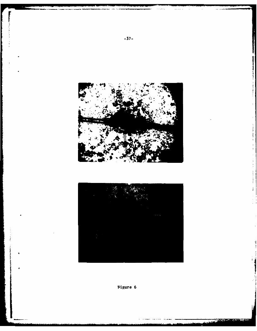
Figure 6 shows color photographs of device #15 after the SiO2 buffer layer
was deposited. The thicker capping SiO 2, which had undergone the thermal
stresses of the out-diffusion temperature plus the etching effects of Li20
vapor, appears as the mottled blue area. The optical channels are under the
brown-orange thin SiO2 buffer.
In parallel with the effort to produce the balanced bridge channel
waveguides in LiNbO f abrication of the asymetric PSCL electrodes by lift-
off was attempted. For practice, a thin SiO 2 film was deposited on a clean
polished LiNbO3 surface and the electrode configuration photolithographically
patterned in negative resist. The developed resist remained in the complement
of the desired electrode pattern. A thin aluminum film was then deposited
over the entire substrate surface and the remaining photoresist stripped.
-37-
Figure 6

-38-
.* In every trial case, the entire aluminum layer lifted off during the strip
stage, indicating poor adhesion of the aluminum to the uncovered substrate
surface. Also, inadequate thickness monitoring equipment resulted in many
films which were too thick and pealed off in a foil.
Despite the lack of previous success, an attempt was made to fabricate
the asyumetric PSCL structure on device #15 with the lift-off technique.
The negative resist was spun on and pre-baked, the electrode photomask
carefully aligned, and the photoresist exposed, developed and post-baked.
Figure 7 shows pictures of the developed photoresist with the electrode
pattern carefully aligned over the branch arms of the optical channel pattern.
Following the deposition of a thin aluminum layer, the photoresist was stripped.
Unfortunately, all metalization again lifted off. The substrate surface was
judged to be sufficiently contaminated that further lift-off attempts would
prove fruitless. Sample #1S was the last available device-sized LiNbO3
substrate at this late stage of the project period.
Despite the inability to fabricate the electrode structure, tests were
performed to verify the optical guiding properties of device #15. The end
faces were polished and, using the now familiar test setup, the light focused
into the end of the input channel appeared as a bright pinpoint at the termina-
tion of the output channel for the guided polarization. Thus, the device was
at least partially transmitting in the unbiased state. To test the function-
*ing of the 3 guide couplers, the substrate was sawed in two transverse to
the propagation direction in the central branched section. This new end face
was polished, and again using the test set up, two piapoints of light could
be observed at the two channel terminations at the output face edge for the
guided polarization.
_ ' i
. . .. . . .. .. . . ... . . . . . . . . . .. . . . . . . . . . . . . . . . . .. .. .. . . . . . . ..." . . .. . . . . . ..l i i 1 i l . . .. .*

-39-
0-0
Figure 71

-40-
Although the asymmetric PSCL could not be fabricated on device #15 by
the liftoff technique, it was still possible to make this microwave line
on a clean blank of LiNbO3 using positive photoresist and an etch technique.
Some tests of the microwave line performances were then made in the absence
of a guided optical signal, as described below.
The asymmetric PSC. was produced by the photolithographically masked
etch of 1200A Aluminum on a clean polished LiNbO3 blank. The metal thickness
was measured by interference microscope. The measured dc resistance of
the line was 11 ohms, somewhat higher than expected. This has been attributed
to the very thin metal layer thickness and to a fabrication flaw which caused
the conducting strir tc narrow at one point. The line was tapered with fixed
ratio of strip width and gap towards the input and output ends for easier
connection with the input and output coaxial cables (semirigid .085 inch).
The co;axlal lines were supported by a brass block, which rested on the pround
Plane electrode. The input VSWR was less than 1.8 in the frequency range
of the test equipment, .5 WIz to 1.3 GlIz. The real criterion for the performance
of the asymmetric PSCL in an integrated optical modulator is not how well
matched it is to the rest of the system, but how efficiently the applied
voltage modulates the light. This can only be measured by the modulation
effects themselves. Unfortunately, without a successful device this proved
to he impossible within the limits of the project period.
t Our calculations estimated a bandwidth of approximately 8 GH for this device.

-41-
IV. CONCLUSION
Within this project, active efforts were made to develop novel means
of design and fabrication of wide bandwidth optical channel waveguide
switch modulators. In particular, we were led to consider an integrated
Mach-Zehnder interferometer (balanced optical bridge) in which wideband
electrooptic electrical signals were synchronously applied through an
axisyumetric coplanar waveguide electrode structure. Our design calcula-
tions show that such an arrangement is of considerable merit in high speed
switching of channel waveguides based on optical materials which possess
moderate-to-small dielectric constants. While several of the device components
were successfully fabricated in the laboratory we were unable to complete the
construction of a fully working LiNbO3-based device within the limits of the
project period. Many useful lessons were nevertheless learned regarding
the fabrication of integrated optical devices with relatively modest equipment
and cost.

-42-
References
[1) L. Goldberg and C. Lee, Rad. Sci. 12, 537 (1977)
[2] R. V. Schmidt and H. Kogelnik, Appl. Phys. Lett. 28, 503 (1976)
(3] II. Kogelnik and R. V. Schmidt, IEEE J. Quant. Fl. QE-12, 396 (1976)
V. Ramaswamy and R. D. Standley, Bell System Tech. J. SS, 767 (1976)
[4] C. P. Wen, IEEE MTT-17, 1087 (1969)
[S] M. Izutsu, Y. Yamane, and T. Sueta, IEEE J. fuant. El. QE-13, 287 (1977)
and M. Tzutsu et. al. IEEE J. Quant. El. OE.-14, 394 (1978)
(6) F. A. J. Marcatili, Bell System Tech. 3. 48, 2071 (1969)
(7] 1. P. Kaminow and L. W. Stulz, Appl. Phys. Lett. 33, 62 (1978)
[8] P. Cross and R. V. Schmidt, IEEE 3. Quant. El. OF-14, 648 (1978)
[9] K. Iwasaki, S. Kurazono, and K. Itakura, Electr. and Comm. in Japan
58-C, 100 (197S)