EFM32GG330 DATASHEET - Silicon Labs - EFM32GG330FXX - d0038_Rev1.40 5 Descriptor-Based...
73
...the world's most energy friendly microcontrollers EFM32GG330 DATASHEET F1024/F512 • ARM Cortex-M3 CPU platform • High Performance 32-bit processor @ up to 48 MHz • Memory Protection Unit • Flexible Energy Management System • 20 nA @ 3 V Shutoff Mode • 0.4 μA @ 3 V Shutoff Mode with RTC • 0.8 μA @ 3 V Stop Mode, including Power-on Reset, Brown-out Detector, RAM and CPU retention • 1.1 μA @ 3 V Deep Sleep Mode, including RTC with 32.768 kHz oscillator, Power-on Reset, Brown-out Detector, RAM and CPU retention • 80 μA/MHz @ 3 V Sleep Mode • 219 μA/MHz @ 3 V Run Mode, with code executed from flash • 1024/512 KB Flash • Read-while-write support • 128 KB RAM • 52 General Purpose I/O pins • Configurable push-pull, open-drain, pull-up/down, input filter, drive strength • Configurable peripheral I/O locations • 16 asynchronous external interrupts • Output state retention and wake-up from Shutoff Mode • 12 Channel DMA Controller • 12 Channel Peripheral Reflex System (PRS) for autonomous in- ter-peripheral signaling • Hardware AES with 128/256-bit keys in 54/75 cycles • Timers/Counters • 4× 16-bit Timer/Counter • 4×3 Compare/Capture/PWM channels • Dead-Time Insertion on TIMER0 • 16-bit Low Energy Timer • 1× 24-bit Real-Time Counter and 1× 32-bit Real-Time Counter • 3× 16/8-bit Pulse Counter with asynchronous operation • Watchdog Timer with dedicated RC oscillator @ 50 nA • Backup Power Domain • RTC and retention registers in a separate power domain, avail- able in all energy modes • Operation from backup battery when main power drains out • Communication interfaces • 3× Universal Synchronous/Asynchronous Receiv- er/Transmitter • UART/SPI/SmartCard (ISO 7816)/IrDA/I2S • 2× Low Energy UART • Autonomous operation with DMA in Deep Sleep Mode • 2× I 2 C Interface with SMBus support • Address recognition in Stop Mode • Universal Serial Bus (USB) with Host & OTG support • Fully USB 2.0 compliant • On-chip PHY and embedded 5V to 3.3V regulator • Ultra low power precision analog peripherals • 12-bit 1 Msamples/s Analog to Digital Converter • 8 single ended channels/4 differential channels • On-chip temperature sensor • 12-bit 500 ksamples/s Digital to Analog Converter • 2 single ended channels/1 differential channel • 2× Analog Comparator • Capacitive sensing with up to 16 inputs • 3× Operational Amplifier • 6.1 MHz GBW, Rail-to-rail, Programmable Gain • Supply Voltage Comparator • Low Energy Sensor Interface (LESENSE) • Autonomous sensor monitoring in Deep Sleep Mode • Wide range of sensors supported, including LC sen- sors and capacitive buttons • Ultra efficient Power-on Reset and Brown-Out Detec- tor • Debug Interface • 2-pin Serial Wire Debug interface • 1-pin Serial Wire Viewer • Embedded Trace Module v3.5 (ETM) • Pre-Programmed USB/UART Bootloader • Temperature range -40 to 85 ºC • Single power supply 1.98 to 3.8 V • QFN64 package 32-bit ARM Cortex-M0+, Cortex-M3 and Cortex-M4 microcontrollers for: • Energy, gas, water and smart metering • Health and fitness applications • Smart accessories • Alarm and security systems • Industrial and home automation
Transcript of EFM32GG330 DATASHEET - Silicon Labs - EFM32GG330FXX - d0038_Rev1.40 5 Descriptor-Based...
...the world's most energy friendly microcontrollers
2016-03-21 - EFM32GG330FXX - d0038_Rev1.40 1 www.silabs.com
EFM32GG330 DATASHEETF1024/F512
• ARM Cortex-M3 CPU platform• High Performance 32-bit processor @ up to 48 MHz• Memory Protection Unit
• Flexible Energy Management System• 20 nA @ 3 V Shutoff Mode• 0.4 µA @ 3 V Shutoff Mode with RTC• 0.8 µA @ 3 V Stop Mode, including Power-on Reset, Brown-out
Detector, RAM and CPU retention• 1.1 µA @ 3 V Deep Sleep Mode, including RTC with 32.768 kHz
oscillator, Power-on Reset, Brown-out Detector, RAM and CPUretention
• 80 µA/MHz @ 3 V Sleep Mode• 219 µA/MHz @ 3 V Run Mode, with code executed from flash
• 1024/512 KB Flash• Read-while-write support
• 128 KB RAM• 52 General Purpose I/O pins
• Configurable push-pull, open-drain, pull-up/down, input filter, drivestrength
• Configurable peripheral I/O locations• 16 asynchronous external interrupts• Output state retention and wake-up from Shutoff Mode
• 12 Channel DMA Controller• 12 Channel Peripheral Reflex System (PRS) for autonomous in-
ter-peripheral signaling• Hardware AES with 128/256-bit keys in 54/75 cycles• Timers/Counters
• 4× 16-bit Timer/Counter• 4×3 Compare/Capture/PWM channels• Dead-Time Insertion on TIMER0
• 16-bit Low Energy Timer• 1× 24-bit Real-Time Counter and 1× 32-bit Real-Time Counter• 3× 16/8-bit Pulse Counter with asynchronous operation• Watchdog Timer with dedicated RC oscillator @ 50 nA
• Backup Power Domain• RTC and retention registers in a separate power domain, avail-
able in all energy modes• Operation from backup battery when main power drains out
• Communication interfaces• 3× Universal Synchronous/Asynchronous Receiv-
er/Transmitter• UART/SPI/SmartCard (ISO 7816)/IrDA/I2S
• 2× Low Energy UART• Autonomous operation with DMA in Deep Sleep
Mode• 2× I2C Interface with SMBus support
• Address recognition in Stop Mode• Universal Serial Bus (USB) with Host & OTG support
• Fully USB 2.0 compliant• On-chip PHY and embedded 5V to 3.3V regulator
• Ultra low power precision analog peripherals• 12-bit 1 Msamples/s Analog to Digital Converter
• 8 single ended channels/4 differential channels• On-chip temperature sensor
• 12-bit 500 ksamples/s Digital to Analog Converter• 2 single ended channels/1 differential channel
• 2× Analog Comparator• Capacitive sensing with up to 16 inputs
• 3× Operational Amplifier• 6.1 MHz GBW, Rail-to-rail, Programmable Gain
• Supply Voltage Comparator• Low Energy Sensor Interface (LESENSE)
• Autonomous sensor monitoring in Deep Sleep Mode• Wide range of sensors supported, including LC sen-
sors and capacitive buttons• Ultra efficient Power-on Reset and Brown-Out Detec-
tor• Debug Interface
• 2-pin Serial Wire Debug interface• 1-pin Serial Wire Viewer
• Embedded Trace Module v3.5 (ETM)• Pre-Programmed USB/UART Bootloader• Temperature range -40 to 85 ºC• Single power supply 1.98 to 3.8 V• QFN64 package
32-bit ARM Cortex-M0+, Cortex-M3 and Cortex-M4 microcontrollers for:
• Energy, gas, water and smart metering• Health and fitness applications• Smart accessories
• Alarm and security systems• Industrial and home automation
...the world's most energy friendly microcontrollers
2016-03-21 - EFM32GG330FXX - d0038_Rev1.40 2 www.silabs.com
1 Ordering InformationTable 1.1 (p. 2) shows the available EFM32GG330 devices.
Table 1.1. Ordering Information
Ordering Code Flash (kB) RAM (kB) MaxSpeed(MHz)
SupplyVoltage(V)
Temperature(ºC)
Package
EFM32GG330F512G-E-QFN64 512 128 48 1.98 - 3.8 -40 - 85 QFN64
EFM32GG330F1024G-E-QFN64 1024 128 48 1.98 - 3.8 -40 - 85 QFN64
Adding the suffix 'R' to the part number (e.g. EFM32GG330F512G-E-QFN64R) denotes tape and reel.
Visit www.silabs.com for information on global distributors and representatives.
...the world's most energy friendly microcontrollers
2016-03-21 - EFM32GG330FXX - d0038_Rev1.40 3 www.silabs.com
2 System Summary
2.1 System Introduction
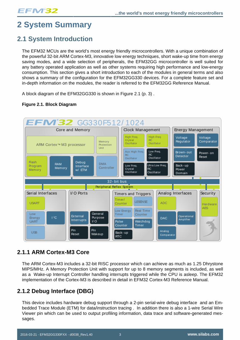
The EFM32 MCUs are the world’s most energy friendly microcontrollers. With a unique combination ofthe powerful 32-bit ARM Cortex-M3, innovative low energy techniques, short wake-up time from energysaving modes, and a wide selection of peripherals, the EFM32GG microcontroller is well suited forany battery operated application as well as other systems requiring high performance and low-energyconsumption. This section gives a short introduction to each of the modules in general terms and alsoshows a summary of the configuration for the EFM32GG330 devices. For a complete feature set andin-depth information on the modules, the reader is referred to the EFM32GG Reference Manual.
A block diagram of the EFM32GG330 is shown in Figure 2.1 (p. 3) .
Figure 2.1. Block Diagram
Clock Management Energy Management
Serial Interfaces I/ O Ports
Core and Memory
Timers and Triggers Analog Interfaces Security
32- bit busPeripheral Reflex System
ARM Cortex™- M3 processor
FlashProgramMemory
LESENSE
High Freq RCOscillator
High Freq. Crystal Oscillator
Timer/Counter
Low EnergyTimer
Pulse Counter
Real TimeCounter
Low Freq. CrystalOscillator
Low Freq. RCOscillator
WatchdogTimer
RAMMemory
GeneralPurposeI/ O
MemoryProtect ionUnit
DMAController
DebugInterfacew/ ETM
ExternalInterrupts
PinReset
HardwareAES
GG330F512/ 1024
ADC
DAC
Analog Comparator
Operat ionalAmplif ier
USART
Low EnergyUART
I 2C
Power- onReset
VoltageRegulator
Back- upPowerDomain
VoltageComparator
Brown- outDetector
Back- upRTC
USBPinWakeup
Ultra Low Freq.RCOscillator
Aux High Freq. RCOscillator
2.1.1 ARM Cortex-M3 Core
The ARM Cortex-M3 includes a 32-bit RISC processor which can achieve as much as 1.25 DhrystoneMIPS/MHz. A Memory Protection Unit with support for up to 8 memory segments is included, as wellas a Wake-up Interrupt Controller handling interrupts triggered while the CPU is asleep. The EFM32implementation of the Cortex-M3 is described in detail in EFM32 Cortex-M3 Reference Manual.
2.1.2 Debug Interface (DBG)
This device includes hardware debug support through a 2-pin serial-wire debug interface and an Em-bedded Trace Module (ETM) for data/instruction tracing . In addition there is also a 1-wire Serial WireViewer pin which can be used to output profiling information, data trace and software-generated mes-sages.
...the world's most energy friendly microcontrollers
2016-03-21 - EFM32GG330FXX - d0038_Rev1.40 4 www.silabs.com
2.1.3 Memory System Controller (MSC)
The Memory System Controller (MSC) is the program memory unit of the EFM32GG microcontroller.The flash memory is readable and writable from both the Cortex-M3 and DMA. The flash memory isdivided into two blocks; the main block and the information block. Program code is normally written tothe main block. Additionally, the information block is available for special user data and flash lock bits.There is also a read-only page in the information block containing system and device calibration data.Read and write operations are supported in the energy modes EM0 and EM1.
2.1.4 Direct Memory Access Controller (DMA)
The Direct Memory Access (DMA) controller performs memory operations independently of the CPU.This has the benefit of reducing the energy consumption and the workload of the CPU, and enablesthe system to stay in low energy modes when moving for instance data from the USART to RAM orfrom the External Bus Interface to a PWM-generating timer. The DMA controller uses the PL230 µDMAcontroller licensed from ARM.
2.1.5 Reset Management Unit (RMU)
The RMU is responsible for handling the reset functionality of the EFM32GG.
2.1.6 Energy Management Unit (EMU)
The Energy Management Unit (EMU) manage all the low energy modes (EM) in EFM32GG microcon-trollers. Each energy mode manages if the CPU and the various peripherals are available. The EMUcan also be used to turn off the power to unused SRAM blocks.
2.1.7 Clock Management Unit (CMU)
The Clock Management Unit (CMU) is responsible for controlling the oscillators and clocks on-board theEFM32GG. The CMU provides the capability to turn on and off the clock on an individual basis to allperipheral modules in addition to enable/disable and configure the available oscillators. The high degreeof flexibility enables software to minimize energy consumption in any specific application by not wastingpower on peripherals and oscillators that are inactive.
2.1.8 Watchdog (WDOG)
The purpose of the watchdog timer is to generate a reset in case of a system failure, to increase appli-cation reliability. The failure may e.g. be caused by an external event, such as an ESD pulse, or by asoftware failure.
2.1.9 Peripheral Reflex System (PRS)
The Peripheral Reflex System (PRS) system is a network which lets the different peripheral modulecommunicate directly with each other without involving the CPU. Peripheral modules which send outReflex signals are called producers. The PRS routes these reflex signals to consumer peripherals whichapply actions depending on the data received. The format for the Reflex signals is not given, but edgetriggers and other functionality can be applied by the PRS.
2.1.10 Universal Serial Bus Controller (USB)
The USB is a full-speed USB 2.0 compliant OTG host/device controller. The USB can be used in Device,On-the-go (OTG) Dual Role Device or Host-only configuration. In OTG mode the USB supports bothHost Negotiation Protocol (HNP) and Session Request Protocol (SRP). The device supports both full-speed (12MBit/s) and low speed (1.5MBit/s) operation. The USB device includes an internal dedicated
...the world's most energy friendly microcontrollers
2016-03-21 - EFM32GG330FXX - d0038_Rev1.40 5 www.silabs.com
Descriptor-Based Scatter/Gather DMA and supports up to 6 OUT endpoints and 6 IN endpoints, inaddition to endpoint 0. The on-chip PHY includes all OTG features, except for the voltage booster forsupplying 5V to VBUS when operating as host.
2.1.11 Inter-Integrated Circuit Interface (I2C)
The I2C module provides an interface between the MCU and a serial I2C-bus. It is capable of acting asboth a master and a slave, and supports multi-master buses. Both standard-mode, fast-mode and fast-mode plus speeds are supported, allowing transmission rates all the way from 10 kbit/s up to 1 Mbit/s.Slave arbitration and timeouts are also provided to allow implementation of an SMBus compliant system.The interface provided to software by the I2C module, allows both fine-grained control of the transmissionprocess and close to automatic transfers. Automatic recognition of slave addresses is provided in allenergy modes.
2.1.12 Universal Synchronous/Asynchronous Receiver/Transmitter (US-ART)
The Universal Synchronous Asynchronous serial Receiver and Transmitter (USART) is a very flexibleserial I/O module. It supports full duplex asynchronous UART communication as well as RS-485, SPI,MicroWire and 3-wire. It can also interface with ISO7816 SmartCards, IrDA and I2S devices.
2.1.13 Pre-Programmed USB/UART Bootloader
The bootloader presented in application note AN0042 is pre-programmed in the device at factory. Thebootloader enables users to program the EFM32 through a UART or a USB CDC class virtual UARTwithout the need for a debugger. The autobaud feature, interface and commands are described furtherin the application note.
2.1.14 Low Energy Universal Asynchronous Receiver/Transmitter(LEUART)
The unique LEUARTTM, the Low Energy UART, is a UART that allows two-way UART communication ona strict power budget. Only a 32.768 kHz clock is needed to allow UART communication up to 9600 baud/s. The LEUART includes all necessary hardware support to make asynchronous serial communicationpossible with minimum of software intervention and energy consumption.
2.1.15 Timer/Counter (TIMER)
The 16-bit general purpose Timer has 3 compare/capture channels for input capture and compare/Pulse-Width Modulation (PWM) output. TIMER0 also includes a Dead-Time Insertion module suitable for motorcontrol applications.
2.1.16 Real Time Counter (RTC)
The Real Time Counter (RTC) contains a 24-bit counter and is clocked either by a 32.768 kHz crystaloscillator, or a 32.768 kHz RC oscillator. In addition to energy modes EM0 and EM1, the RTC is alsoavailable in EM2. This makes it ideal for keeping track of time since the RTC is enabled in EM2 wheremost of the device is powered down.
2.1.17 Backup Real Time Counter (BURTC)
The Backup Real Time Counter (BURTC) contains a 32-bit counter and is clocked either by a 32.768 kHzcrystal oscillator, a 32.768 kHz RC oscillator or a 1 kHz ULFRCO. The BURTC is available in all EnergyModes and it can also run in backup mode, making it operational even if the main power should drain out.
...the world's most energy friendly microcontrollers
2016-03-21 - EFM32GG330FXX - d0038_Rev1.40 6 www.silabs.com
2.1.18 Low Energy Timer (LETIMER)
The unique LETIMERTM, the Low Energy Timer, is a 16-bit timer that is available in energy mode EM2in addition to EM1 and EM0. Because of this, it can be used for timing and output generation when mostof the device is powered down, allowing simple tasks to be performed while the power consumption ofthe system is kept at an absolute minimum. The LETIMER can be used to output a variety of waveformswith minimal software intervention. It is also connected to the Real Time Counter (RTC), and can beconfigured to start counting on compare matches from the RTC.
2.1.19 Pulse Counter (PCNT)
The Pulse Counter (PCNT) can be used for counting pulses on a single input or to decode quadratureencoded inputs. It runs off either the internal LFACLK or the PCNTn_S0IN pin as external clock source.The module may operate in energy mode EM0 - EM3.
2.1.20 Analog Comparator (ACMP)
The Analog Comparator is used to compare the voltage of two analog inputs, with a digital output indi-cating which input voltage is higher. Inputs can either be one of the selectable internal references or fromexternal pins. Response time and thereby also the current consumption can be configured by alteringthe current supply to the comparator.
2.1.21 Voltage Comparator (VCMP)
The Voltage Supply Comparator is used to monitor the supply voltage from software. An interrupt canbe generated when the supply falls below or rises above a programmable threshold. Response time andthereby also the current consumption can be configured by altering the current supply to the comparator.
2.1.22 Analog to Digital Converter (ADC)
The ADC is a Successive Approximation Register (SAR) architecture, with a resolution of up to 12 bitsat up to one million samples per second. The integrated input mux can select inputs from 8 externalpins and 6 internal signals.
2.1.23 Digital to Analog Converter (DAC)
The Digital to Analog Converter (DAC) can convert a digital value to an analog output voltage. The DACis fully differential rail-to-rail, with 12-bit resolution. It has two single ended output buffers which can becombined into one differential output. The DAC may be used for a number of different applications suchas sensor interfaces or sound output.
2.1.24 Operational Amplifier (OPAMP)
The EFM32GG330 features 3 Operational Amplifiers. The Operational Amplifier is a versatile generalpurpose amplifier with rail-to-rail differential input and rail-to-rail single ended output. The input can be setto pin, DAC or OPAMP, whereas the output can be pin, OPAMP or ADC. The current is programmableand the OPAMP has various internal configurations such as unity gain, programmable gain using internalresistors etc.
2.1.25 Low Energy Sensor Interface (LESENSE)
The Low Energy Sensor Interface (LESENSETM), is a highly configurable sensor interface with supportfor up to 16 individually configurable sensors. By controlling the analog comparators and DAC, LESENSEis capable of supporting a wide range of sensors and measurement schemes, and can for instance mea-sure LC sensors, resistive sensors and capacitive sensors. LESENSE also includes a programmableFSM which enables simple processing of measurement results without CPU intervention. LESENSE is
...the world's most energy friendly microcontrollers
2016-03-21 - EFM32GG330FXX - d0038_Rev1.40 7 www.silabs.com
available in energy mode EM2, in addition to EM0 and EM1, making it ideal for sensor monitoring inapplications with a strict energy budget.
2.1.26 Backup Power Domain
The backup power domain is a separate power domain containing a Backup Real Time Counter, BURTC,and a set of retention registers, available in all energy modes. This power domain can be configured toautomatically change power source to a backup battery when the main power drains out. The backuppower domain enables the EFM32GG330 to keep track of time and retain data, even if the main powersource should drain out.
2.1.27 Advanced Encryption Standard Accelerator (AES)
The AES accelerator performs AES encryption and decryption with 128-bit or 256-bit keys. Encrypting ordecrypting one 128-bit data block takes 52 HFCORECLK cycles with 128-bit keys and 75 HFCORECLKcycles with 256-bit keys. The AES module is an AHB slave which enables efficient access to the dataand key registers. All write accesses to the AES module must be 32-bit operations, i.e. 8- or 16-bitoperations are not supported.
2.1.28 General Purpose Input/Output (GPIO)
In the EFM32GG330, there are 52 General Purpose Input/Output (GPIO) pins, which are divided intoports with up to 16 pins each. These pins can individually be configured as either an output or input. Moreadvanced configurations like open-drain, filtering and drive strength can also be configured individuallyfor the pins. The GPIO pins can also be overridden by peripheral pin connections, like Timer PWMoutputs or USART communication, which can be routed to several locations on the device. The GPIOsupports up to 16 asynchronous external pin interrupts, which enables interrupts from any pin on thedevice. Also, the input value of a pin can be routed through the Peripheral Reflex System to otherperipherals.
2.2 Configuration Summary
The features of the EFM32GG330 is a subset of the feature set described in the EFM32GG ReferenceManual. Table 2.1 (p. 7) describes device specific implementation of the features.
Table 2.1. Configuration Summary
Module Configuration Pin Connections
Cortex-M3 Full configuration NA
DBG Full configuration DBG_SWCLK, DBG_SWDIO,DBG_SWO
MSC Full configuration NA
DMA Full configuration NA
RMU Full configuration NA
EMU Full configuration NA
CMU Full configuration CMU_OUT0, CMU_OUT1
WDOG Full configuration NA
PRS Full configuration NA
USB Full configuration USB_VBUS, USB_VBUSEN,USB_VREGI, USB_VREGO, USB_DM,USB_DMPU, USB_DP, USB_ID
...the world's most energy friendly microcontrollers
2016-03-21 - EFM32GG330FXX - d0038_Rev1.40 8 www.silabs.com
Module Configuration Pin Connections
I2C0 Full configuration I2C0_SDA, I2C0_SCL
I2C1 Full configuration I2C1_SDA, I2C1_SCL
USART0 Full configuration with IrDA US0_TX, US0_RX. US0_CLK, US0_CS
USART1 Full configuration with I2S US1_TX, US1_RX, US1_CLK, US1_CS
USART2 Full configuration with I2S US2_TX, US2_RX, US2_CLK, US2_CS
LEUART0 Full configuration LEU0_TX, LEU0_RX
LEUART1 Full configuration LEU1_TX, LEU1_RX
TIMER0 Full configuration with DTI TIM0_CC[2:0], TIM0_CDTI[2:0]
TIMER1 Full configuration TIM1_CC[2:0]
TIMER2 Full configuration TIM2_CC[2:0]
TIMER3 Full configuration TIM3_CC[2:0]
RTC Full configuration NA
BURTC Full configuration NA
LETIMER0 Full configuration LET0_O[1:0]
PCNT0 Full configuration, 16-bit count register PCNT0_S[1:0]
PCNT1 Full configuration, 8-bit count register PCNT1_S[1:0]
PCNT2 Full configuration, 8-bit count register PCNT2_S[1:0]
ACMP0 Full configuration ACMP0_CH[7:0], ACMP0_O
ACMP1 Full configuration ACMP1_CH[7:0], ACMP1_O
VCMP Full configuration NA
ADC0 Full configuration ADC0_CH[7:0]
DAC0 Full configuration DAC0_OUT[1:0], DAC0_OUTxALT
OPAMP Full configuration Outputs: OPAMP_OUTx,OPAMP_OUTxALT, Inputs:OPAMP_Px, OPAMP_Nx
AES Full configuration NA
GPIO 52 pins Available pins are shown inTable 4.3 (p. 56)
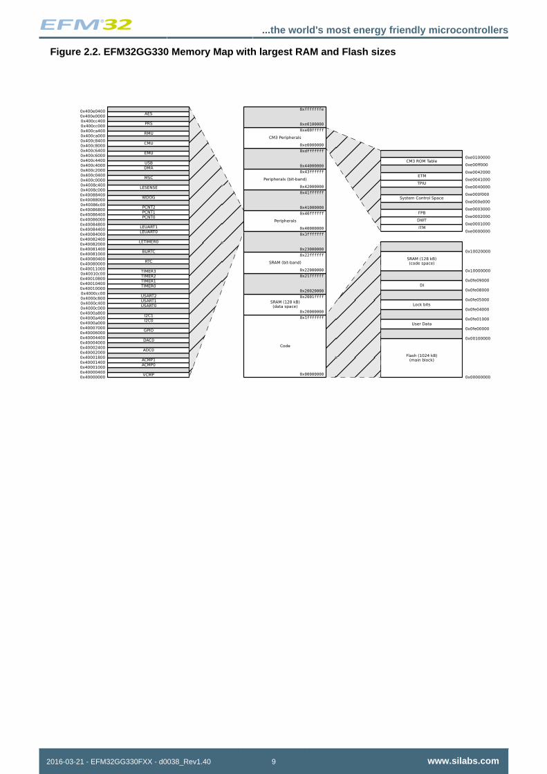
2.3 Memory Map
The EFM32GG330 memory map is shown in Figure 2.2 (p. 9) , with RAM and Flash sizes for thelargest memory configuration.
...the world's most energy friendly microcontrollers
2016-03-21 - EFM32GG330FXX - d0038_Rev1.40 9 www.silabs.com
Figure 2.2. EFM32GG330 Memory Map with largest RAM and Flash sizes
...the world's most energy friendly microcontrollers
2016-03-21 - EFM32GG330FXX - d0038_Rev1.40 10 www.silabs.com
3 Electrical Characteristics
3.1 Test Conditions
3.1.1 Typical Values
The typical data are based on TAMB=25°C and VDD=3.0 V, as defined in Table 3.2 (p. 10) , unlessotherwise specified.
3.1.2 Minimum and Maximum Values
The minimum and maximum values represent the worst conditions of ambient temperature, supply volt-age and frequencies, as defined in Table 3.2 (p. 10) , unless otherwise specified.
3.2 Absolute Maximum Ratings
The absolute maximum ratings are stress ratings, and functional operation under such conditions arenot guaranteed. Stress beyond the limits specified in Table 3.1 (p. 10) may affect the device reliabilityor cause permanent damage to the device. Functional operating conditions are given in Table 3.2 (p.10) .
Table 3.1. Absolute Maximum Ratings
Symbol Parameter Condition Min Typ Max Unit
TSTG Storage tempera-ture range
-40 150 °C
TS Maximum solderingtemperature
Latest IPC/JEDEC J-STD-020Standard
260 °C
VDDMAX External main sup-ply voltage
0 3.8 V
VIOPIN Voltage on any I/Opin
-0.3 VDD+0.3 V
Current per I/O pin(sink)
100 mA
IIOMAXCurrent per I/O pin(source)
-100 mA
3.3 General Operating Conditions
3.3.1 General Operating Conditions
Table 3.2. General Operating Conditions
Symbol Parameter Min Typ Max Unit
TAMB Ambient temperature range -40 85 °C
VDDOP Operating supply voltage 1.98 3.8 V
fAPB Internal APB clock frequency 48 MHz
fAHB Internal AHB clock frequency 48 MHz
...the world's most energy friendly microcontrollers
2016-03-21 - EFM32GG330FXX - d0038_Rev1.40 11 www.silabs.com
3.4 Current Consumption
Table 3.3. Current Consumption
Symbol Parameter Condition Min Typ Max Unit
48 MHz HFXO, all peripheralclocks disabled, VDD= 3.0 V
219 240 µA/MHz
28 MHz HFRCO, all peripheralclocks disabled, VDD= 3.0 V
205 225 µA/MHz
21 MHz HFRCO, all peripheralclocks disabled, VDD= 3.0 V
206 229 µA/MHz
14 MHz HFRCO, all peripheralclocks disabled, VDD= 3.0 V
209 232 µA/MHz
11 MHz HFRCO, all peripheralclocks disabled, VDD= 3.0 V
211 234 µA/MHz
6.6 MHz HFRCO, all peripheralclocks disabled, VDD= 3.0 V
215 242 µA/MHz
IEM0
EM0 current. Noprescaling. Run-ning prime num-ber calculation codefrom flash. (Produc-tion test condition =14MHz)
1.2 MHz HFRCO, all peripheralclocks disabled, VDD= 3.0 V
243 327 µA/MHz
48 MHz HFXO, all peripheralclocks disabled, VDD= 3.0 V
80 90 µA/MHz
28 MHz HFRCO, all peripheralclocks disabled, VDD= 3.0 V
80 90 µA/MHz
21 MHz HFRCO, all peripheralclocks disabled, VDD= 3.0 V
81 91 µA/MHz
14 MHz HFRCO, all peripheralclocks disabled, VDD= 3.0 V
83 99 µA/MHz
11 MHz HFRCO, all peripheralclocks disabled, VDD= 3.0 V
85 100 µA/MHz
6.6 MHz HFRCO, all peripheralclocks disabled, VDD= 3.0 V
90 102 µA/MHz
IEM1
EM1 current (Pro-duction test condi-tion = 14MHz)
1.2 MHz HFRCO. all peripheralclocks disabled, VDD= 3.0 V
122 152 µA/MHz
EM2 current with RTCprescaled to 1 Hz, 32.768kHz LFRCO, VDD= 3.0 V,TAMB=25°C
1.11 1.91 µA
IEM2 EM2 currentEM2 current with RTCprescaled to 1 Hz, 32.768kHz LFRCO, VDD= 3.0 V,TAMB=85°C
8.81 21.51 µA
VDD= 3.0 V, TAMB=25°C 0.81 1.51 µAIEM3 EM3 current
VDD= 3.0 V, TAMB=85°C 8.21 20.31 µA
VDD= 3.0 V, TAMB=25°C 0.02 0.08 µAIEM4 EM4 current
VDD= 3.0 V, TAMB=85°C 0.5 2.5 µA1Only one RAM block enabled. The RAM block size is 32 kB.
...the world's most energy friendly microcontrollers
2016-03-21 - EFM32GG330FXX - d0038_Rev1.40 12 www.silabs.com
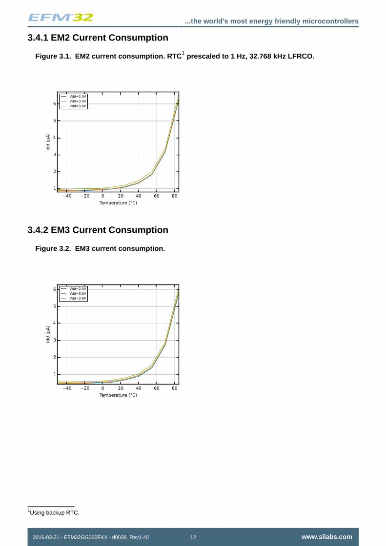
3.4.1 EM2 Current Consumption
Figure 3.1. EM2 current consumption. RTC1 prescaled to 1 Hz, 32.768 kHz LFRCO.
3.4.2 EM3 Current Consumption
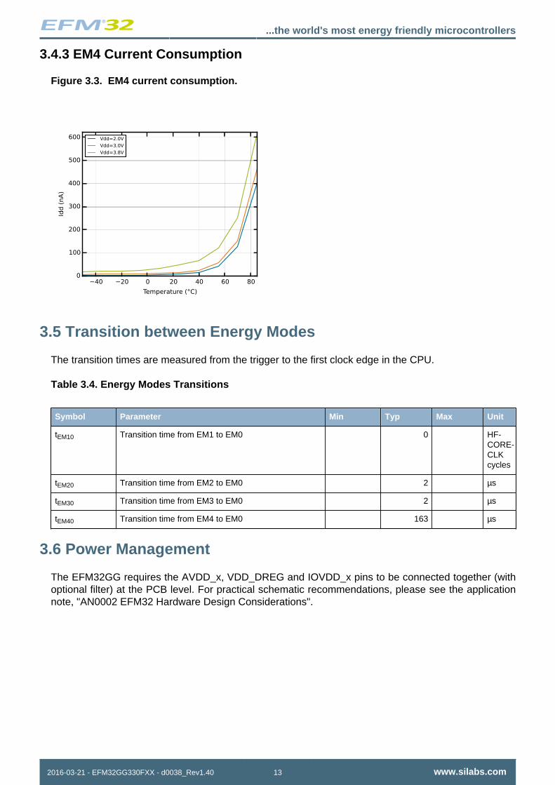
Figure 3.2. EM3 current consumption.
1Using backup RTC.
...the world's most energy friendly microcontrollers
2016-03-21 - EFM32GG330FXX - d0038_Rev1.40 13 www.silabs.com
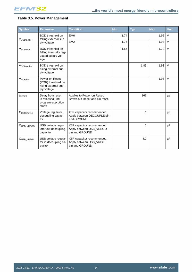
3.4.3 EM4 Current Consumption
Figure 3.3. EM4 current consumption.
3.5 Transition between Energy Modes
The transition times are measured from the trigger to the first clock edge in the CPU.
Table 3.4. Energy Modes Transitions
Symbol Parameter Min Typ Max Unit
tEM10 Transition time from EM1 to EM0 0 HF-CORE-CLKcycles
tEM20 Transition time from EM2 to EM0 2 µs
tEM30 Transition time from EM3 to EM0 2 µs
tEM40 Transition time from EM4 to EM0 163 µs
3.6 Power Management
The EFM32GG requires the AVDD_x, VDD_DREG and IOVDD_x pins to be connected together (withoptional filter) at the PCB level. For practical schematic recommendations, please see the applicationnote, "AN0002 EFM32 Hardware Design Considerations".
...the world's most energy friendly microcontrollers
2016-03-21 - EFM32GG330FXX - d0038_Rev1.40 14 www.silabs.com
Table 3.5. Power Management
Symbol Parameter Condition Min Typ Max Unit
EM0 1.74 1.96 VVBODextthr-
BOD threshold onfalling external sup-ply voltage EM2 1.74 1.98 V
VBODintthr- BOD threshold onfalling internally reg-ulated supply volt-age
1.57 1.70 V
VBODextthr+ BOD threshold onrising external sup-ply voltage
1.85 1.98 V
VPORthr+ Power-on Reset(POR) threshold onrising external sup-ply voltage
1.98 V
tRESET Delay from resetis released untilprogram executionstarts
Applies to Power-on Reset,Brown-out Reset and pin reset.
163 µs
CDECOUPLE Voltage regulatordecoupling capaci-tor.
X5R capacitor recommended.Apply between DECOUPLE pinand GROUND
1 µF
CUSB_VREGO USB voltage regu-lator out decouplingcapacitor.
X5R capacitor recommended.Apply between USB_VREGOpin and GROUND
1 µF
CUSB_VREGI USB voltage regula-tor in decoupling ca-pacitor.
X5R capacitor recommended.Apply between USB_VREGIpin and GROUND
4.7 µF
...the world's most energy friendly microcontrollers
2016-03-21 - EFM32GG330FXX - d0038_Rev1.40 15 www.silabs.com
3.7 Flash
Table 3.6. Flash
Symbol Parameter Condition Min Typ Max Unit
ECFLASH Flash erase cyclesbefore failure
20000 cycles
TAMB<150°C 10000 h
TAMB<85°C 10 yearsRETFLASH Flash data retention
TAMB<70°C 20 years
tW_PROG Word (32-bit) pro-gramming time
20 µs
LPERASE == 0 20 20.4 20.8 mstPERASE Page erase time
LPERASE == 1 40 40.4 40.8 ms
tDERASE Device erase time 161.6 ms
LPERASE == 0 141 mAIERASE Erase current
LPERASE == 1 71 mA
LPWRITE == 0 141 mAIWRITE Write current
LPWRITE == 1 71 mA
VFLASH Supply voltage dur-ing flash erase andwrite
1.98 3.8 V
1Measured at 25°C
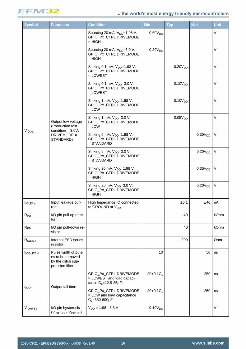
3.8 General Purpose Input Output
Table 3.7. GPIO
Symbol Parameter Condition Min Typ Max Unit
VIOIL Input low voltage 0.30VDD V
VIOIH Input high voltage 0.70VDD V
Sourcing 0.1 mA, VDD=1.98 V,GPIO_Px_CTRL DRIVEMODE= LOWEST
0.80VDD V
Sourcing 0.1 mA, VDD=3.0 V,GPIO_Px_CTRL DRIVEMODE= LOWEST
0.90VDD V
Sourcing 1 mA, VDD=1.98 V,GPIO_Px_CTRL DRIVEMODE= LOW
0.85VDD V
Sourcing 1 mA, VDD=3.0 V,GPIO_Px_CTRL DRIVEMODE= LOW
0.90VDD V
Sourcing 6 mA, VDD=1.98 V,GPIO_Px_CTRL DRIVEMODE= STANDARD
0.75VDD V
VIOOH
Output high volt-age (Production testcondition = 3.0V,DRIVEMODE =STANDARD)
Sourcing 6 mA, VDD=3.0 V,GPIO_Px_CTRL DRIVEMODE= STANDARD
0.85VDD V
...the world's most energy friendly microcontrollers
2016-03-21 - EFM32GG330FXX - d0038_Rev1.40 16 www.silabs.com
Symbol Parameter Condition Min Typ Max Unit
Sourcing 20 mA, VDD=1.98 V,GPIO_Px_CTRL DRIVEMODE= HIGH
0.60VDD V
Sourcing 20 mA, VDD=3.0 V,GPIO_Px_CTRL DRIVEMODE= HIGH
0.80VDD V
Sinking 0.1 mA, VDD=1.98 V,GPIO_Px_CTRL DRIVEMODE= LOWEST
0.20VDD V
Sinking 0.1 mA, VDD=3.0 V,GPIO_Px_CTRL DRIVEMODE= LOWEST
0.10VDD V
Sinking 1 mA, VDD=1.98 V,GPIO_Px_CTRL DRIVEMODE= LOW
0.10VDD V
Sinking 1 mA, VDD=3.0 V,GPIO_Px_CTRL DRIVEMODE= LOW
0.05VDD V
Sinking 6 mA, VDD=1.98 V,GPIO_Px_CTRL DRIVEMODE= STANDARD
0.30VDD V
Sinking 6 mA, VDD=3.0 V,GPIO_Px_CTRL DRIVEMODE= STANDARD
0.20VDD V
Sinking 20 mA, VDD=1.98 V,GPIO_Px_CTRL DRIVEMODE= HIGH
0.35VDD V
VIOOL
Output low voltage(Production testcondition = 3.0V,DRIVEMODE =STANDARD)
Sinking 20 mA, VDD=3.0 V,GPIO_Px_CTRL DRIVEMODE= HIGH
0.20VDD V
IIOLEAK Input leakage cur-rent
High Impedance IO connectedto GROUND or VDD
±0.1 ±40 nA
RPU I/O pin pull-up resis-tor
40 kOhm
RPD I/O pin pull-down re-sistor
40 kOhm
RIOESD Internal ESD seriesresistor
200 Ohm
tIOGLITCH Pulse width of puls-es to be removedby the glitch sup-pression filter
10 50 ns
GPIO_Px_CTRL DRIVEMODE= LOWEST and load capaci-tance CL=12.5-25pF.
20+0.1CL 250 ns
tIOOF Output fall timeGPIO_Px_CTRL DRIVEMODE= LOW and load capacitanceCL=350-600pF
20+0.1CL 250 ns
VIOHYST I/O pin hysteresis(VIOTHR+ - VIOTHR-)
VDD = 1.98 - 3.8 V 0.10VDD V
...the world's most energy friendly microcontrollers
2016-03-21 - EFM32GG330FXX - d0038_Rev1.40 17 www.silabs.com
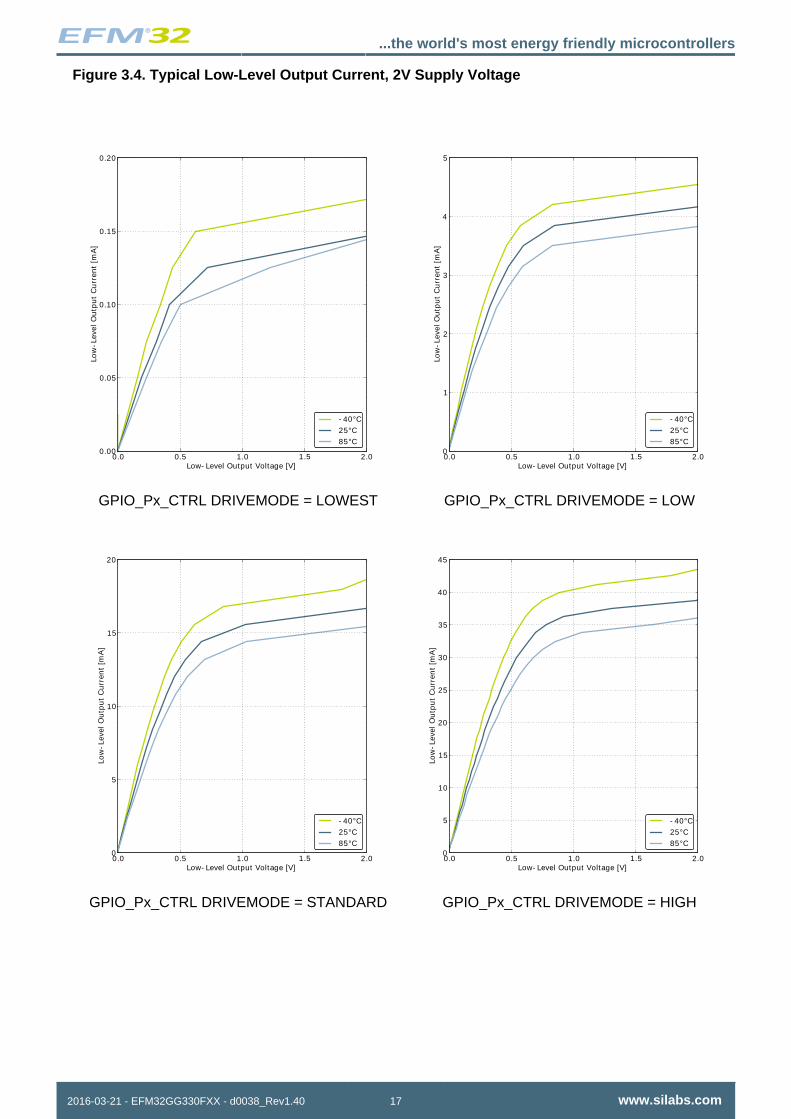
Figure 3.4. Typical Low-Level Output Current, 2V Supply Voltage
0.0 0.5 1.0 1.5 2.0Low- Level Output Voltage [V]
0.00
0.05
0.10
0.15
0.20
Low
-Le
vel
Ou
tpu
t C
urr
ent
[mA
]
- 40°C
25°C
85°C
GPIO_Px_CTRL DRIVEMODE = LOWEST
0.0 0.5 1.0 1.5 2.0Low- Level Output Voltage [V]
0
1
2
3
4
5
Low
-Le
vel
Ou
tpu
t C
urr
ent
[mA
]
- 40°C
25°C
85°C
GPIO_Px_CTRL DRIVEMODE = LOW
0.0 0.5 1.0 1.5 2.0Low- Level Output Voltage [V]
0
5
10
15
20
Low
-Le
vel
Ou
tpu
t C
urr
ent
[mA
]
- 40°C
25°C
85°C
GPIO_Px_CTRL DRIVEMODE = STANDARD
0.0 0.5 1.0 1.5 2.0Low- Level Output Voltage [V]
0
5
10
15
20
25
30
35
40
45
Low
-Le
vel
Ou
tpu
t C
urr
ent
[mA
]
- 40°C
25°C
85°C
GPIO_Px_CTRL DRIVEMODE = HIGH
...the world's most energy friendly microcontrollers
2016-03-21 - EFM32GG330FXX - d0038_Rev1.40 18 www.silabs.com
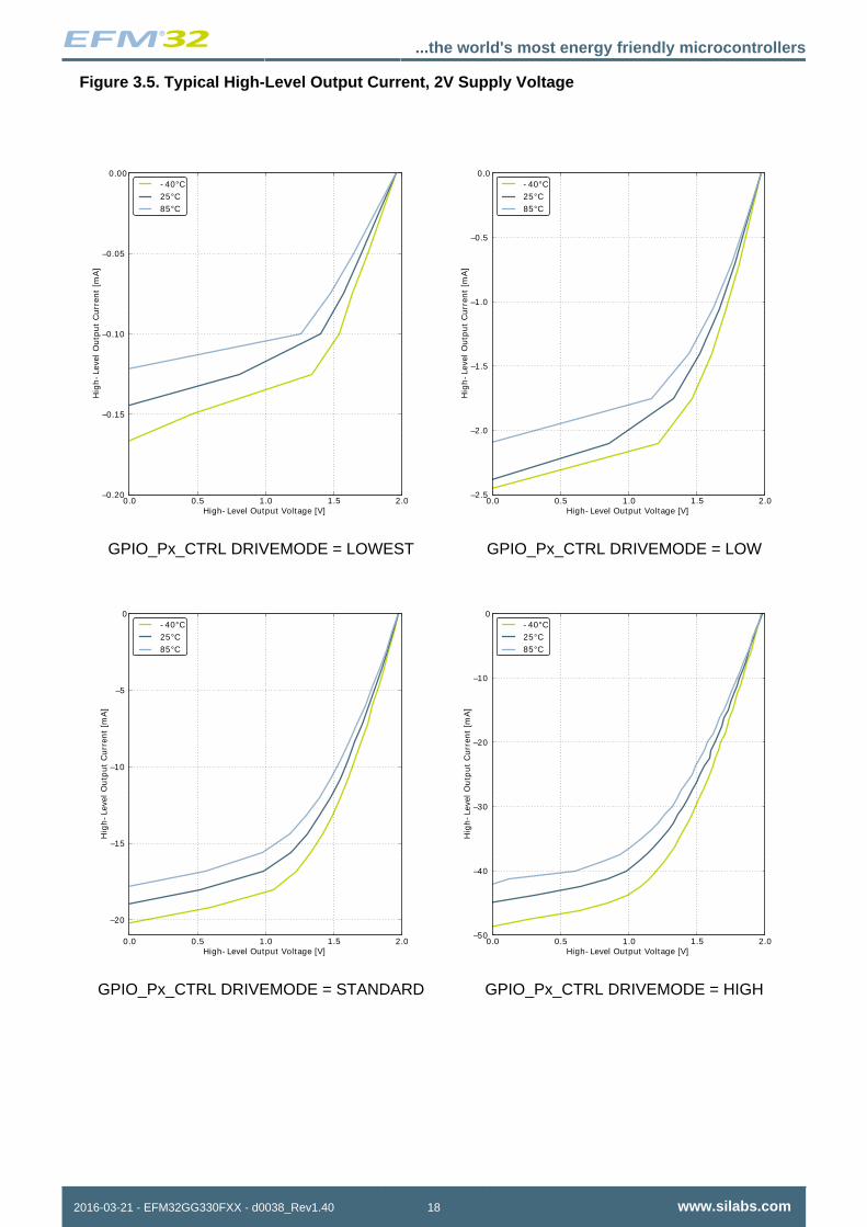
Figure 3.5. Typical High-Level Output Current, 2V Supply Voltage
0.0 0.5 1.0 1.5 2.0High- Level Output Voltage [V]
–0.20
–0.15
–0.10
–0.05
0.00
Hig
h-
Leve
l O
utp
ut
Cu
rren
t [m
A]
- 40°C
25°C
85°C
GPIO_Px_CTRL DRIVEMODE = LOWEST
0.0 0.5 1.0 1.5 2.0High- Level Output Voltage [V]
–2.5
–2.0
–1.5
–1.0
–0.5
0.0
Hig
h-
Leve
l O
utp
ut
Cu
rren
t [m
A]
- 40°C
25°C
85°C
GPIO_Px_CTRL DRIVEMODE = LOW
0.0 0.5 1.0 1.5 2.0High- Level Output Voltage [V]
–20
–15
–10
–5
0
Hig
h-
Leve
l O
utp
ut
Cu
rren
t [m
A]
- 40°C
25°C
85°C
GPIO_Px_CTRL DRIVEMODE = STANDARD
0.0 0.5 1.0 1.5 2.0High- Level Output Voltage [V]
–50
–40
–30
–20
–10
0
Hig
h-
Leve
l O
utp
ut
Cu
rren
t [m
A]
- 40°C
25°C
85°C
GPIO_Px_CTRL DRIVEMODE = HIGH
...the world's most energy friendly microcontrollers
2016-03-21 - EFM32GG330FXX - d0038_Rev1.40 19 www.silabs.com
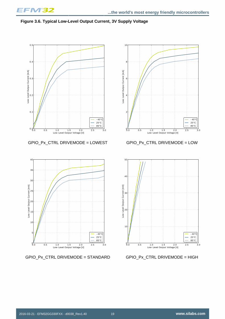
Figure 3.6. Typical Low-Level Output Current, 3V Supply Voltage
0.0 0.5 1.0 1.5 2.0 2.5 3.0Low- Level Output Voltage [V]
0.0
0.1
0.2
0.3
0.4
0.5
Low
-Le
vel
Ou
tpu
t C
urr
ent
[mA
]
- 40°C
25°C
85°C
GPIO_Px_CTRL DRIVEMODE = LOWEST
0.0 0.5 1.0 1.5 2.0 2.5 3.0Low- Level Output Voltage [V]
0
2
4
6
8
10
Low
-Le
vel
Ou
tpu
t C
urr
ent
[mA
]
- 40°C
25°C
85°C
GPIO_Px_CTRL DRIVEMODE = LOW
0.0 0.5 1.0 1.5 2.0 2.5 3.0Low- Level Output Voltage [V]
0
5
10
15
20
25
30
35
40
Low
-Le
vel
Ou
tpu
t C
urr
ent
[mA
]
- 40°C
25°C
85°C
GPIO_Px_CTRL DRIVEMODE = STANDARD
0.0 0.5 1.0 1.5 2.0 2.5 3.0Low- Level Output Voltage [V]
0
10
20
30
40
50
Low
-Le
vel
Ou
tpu
t C
urr
ent
[mA
]
- 40°C
25°C
85°C
GPIO_Px_CTRL DRIVEMODE = HIGH
...the world's most energy friendly microcontrollers
2016-03-21 - EFM32GG330FXX - d0038_Rev1.40 20 www.silabs.com
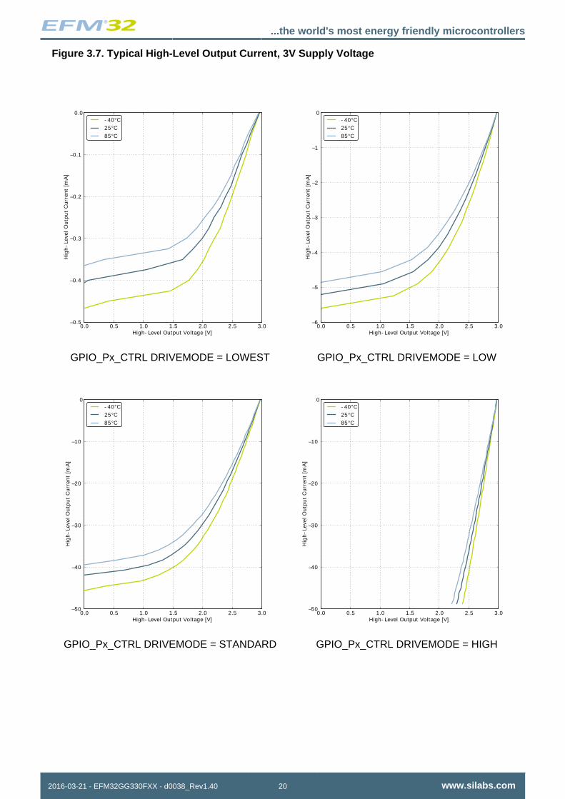
Figure 3.7. Typical High-Level Output Current, 3V Supply Voltage
0.0 0.5 1.0 1.5 2.0 2.5 3.0High- Level Output Voltage [V]
–0.5
–0.4
–0.3
–0.2
–0.1
0.0
Hig
h-
Leve
l O
utp
ut
Cu
rren
t [m
A]
- 40°C
25°C
85°C
GPIO_Px_CTRL DRIVEMODE = LOWEST
0.0 0.5 1.0 1.5 2.0 2.5 3.0High- Level Output Voltage [V]
–6
–5
–4
–3
–2
–1
0
Hig
h-
Leve
l O
utp
ut
Cu
rren
t [m
A]
- 40°C
25°C
85°C
GPIO_Px_CTRL DRIVEMODE = LOW
0.0 0.5 1.0 1.5 2.0 2.5 3.0High- Level Output Voltage [V]
–50
–40
–30
–20
–10
0
Hig
h-
Leve
l O
utp
ut
Cu
rren
t [m
A]
- 40°C
25°C
85°C
GPIO_Px_CTRL DRIVEMODE = STANDARD
0.0 0.5 1.0 1.5 2.0 2.5 3.0High- Level Output Voltage [V]
–50
–40
–30
–20
–10
0
Hig
h-
Leve
l O
utp
ut
Cu
rren
t [m
A]
- 40°C
25°C
85°C
GPIO_Px_CTRL DRIVEMODE = HIGH
...the world's most energy friendly microcontrollers
2016-03-21 - EFM32GG330FXX - d0038_Rev1.40 21 www.silabs.com
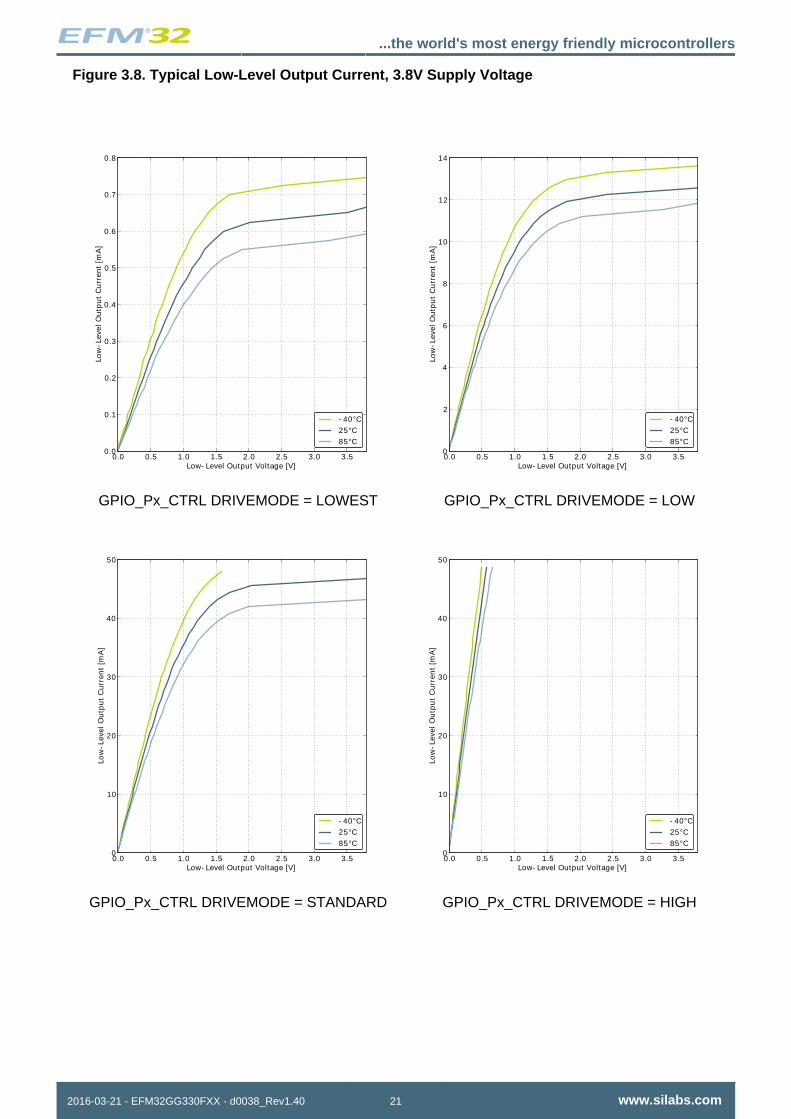
Figure 3.8. Typical Low-Level Output Current, 3.8V Supply Voltage
0.0 0.5 1.0 1.5 2.0 2.5 3.0 3.5Low- Level Output Voltage [V]
0.0
0.1
0.2
0.3
0.4
0.5
0.6
0.7
0.8
Low
-Le
vel
Ou
tpu
t C
urr
ent
[mA
]
- 40°C
25°C
85°C
GPIO_Px_CTRL DRIVEMODE = LOWEST
0.0 0.5 1.0 1.5 2.0 2.5 3.0 3.5Low- Level Output Voltage [V]
0
2
4
6
8
10
12
14
Low
-Le
vel
Ou
tpu
t C
urr
ent
[mA
]
- 40°C
25°C
85°C
GPIO_Px_CTRL DRIVEMODE = LOW
0.0 0.5 1.0 1.5 2.0 2.5 3.0 3.5Low- Level Output Voltage [V]
0
10
20
30
40
50
Low
-Le
vel
Ou
tpu
t C
urr
ent
[mA
]
- 40°C
25°C
85°C
GPIO_Px_CTRL DRIVEMODE = STANDARD
0.0 0.5 1.0 1.5 2.0 2.5 3.0 3.5Low- Level Output Voltage [V]
0
10
20
30
40
50
Low
-Le
vel
Ou
tpu
t C
urr
ent
[mA
]
- 40°C
25°C
85°C
GPIO_Px_CTRL DRIVEMODE = HIGH
...the world's most energy friendly microcontrollers
2016-03-21 - EFM32GG330FXX - d0038_Rev1.40 22 www.silabs.com
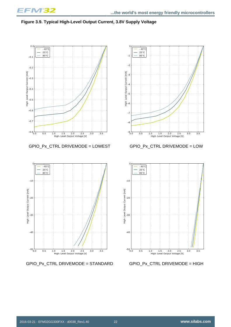
Figure 3.9. Typical High-Level Output Current, 3.8V Supply Voltage
0.0 0.5 1.0 1.5 2.0 2.5 3.0 3.5High- Level Output Voltage [V]
–0.8
–0.7
–0.6
–0.5
–0.4
–0.3
–0.2
–0.1
0.0
Hig
h-
Leve
l O
utp
ut
Cu
rren
t [m
A]
- 40°C
25°C
85°C
GPIO_Px_CTRL DRIVEMODE = LOWEST
0.0 0.5 1.0 1.5 2.0 2.5 3.0 3.5High- Level Output Voltage [V]
–9
–8
–7
–6
–5
–4
–3
–2
–1
0
Hig
h-
Leve
l O
utp
ut
Cu
rren
t [m
A]
- 40°C
25°C
85°C
GPIO_Px_CTRL DRIVEMODE = LOW
0.0 0.5 1.0 1.5 2.0 2.5 3.0 3.5High- Level Output Voltage [V]
–50
–40
–30
–20
–10
0
Hig
h-
Leve
l O
utp
ut
Cu
rren
t [m
A]
- 40°C
25°C
85°C
GPIO_Px_CTRL DRIVEMODE = STANDARD
0.0 0.5 1.0 1.5 2.0 2.5 3.0 3.5High- Level Output Voltage [V]
–50
–40
–30
–20
–10
0
Hig
h-
Leve
l O
utp
ut
Cu
rren
t [m
A]
- 40°C
25°C
85°C
GPIO_Px_CTRL DRIVEMODE = HIGH
...the world's most energy friendly microcontrollers
2016-03-21 - EFM32GG330FXX - d0038_Rev1.40 23 www.silabs.com
3.9 Oscillators
3.9.1 LFXO
Table 3.8. LFXO
Symbol Parameter Condition Min Typ Max Unit
fLFXO Supported nominalcrystal frequency
32.768 kHz
ESRLFXO Supported crystalequivalent series re-sistance (ESR)
30 120 kOhm
CLFXOL Supported crystalexternal load range
X1 25 pF
DCLFXO Duty cycle 48 50 53.5 %
ILFXO Current consump-tion for core andbuffer after startup.
ESR=30 kOhm, CL=10 pF,LFXOBOOST in CMU_CTRL is1
190 nA
tLFXO Start- up time. ESR=30 kOhm, CL=10 pF,40% - 60% duty cycle hasbeen reached, LFXOBOOST inCMU_CTRL is 1
400 ms
1See Minimum Load Capacitance (CLFXOL) Requirement For Safe Crystal Startup in energyAware Designer in Simplicity Studio
For safe startup of a given crystal, the Configurator tool in Simplicity Studio contains a tool to helpusers configure both load capacitance and software settings for using the LFXO. For details regardingthe crystal configuration, the reader is referred to application note "AN0016 EFM32 Oscillator DesignConsideration".
3.9.2 HFXO
Table 3.9. HFXO
Symbol Parameter Condition Min Typ Max Unit
fHFXO Supported nominalcrystal Frequency
4 48 MHz
Crystal frequency 48 MHz 50 Ohm
Crystal frequency 32 MHz 30 60 OhmESRHFXO
Supported crystalequivalent series re-sistance (ESR)
Crystal frequency 4 MHz 400 1500 Ohm
gmHFXO The transconduc-tance of the HFXOinput transistor atcrystal startup
HFXOBOOST in CMU_CTRLequals 0b11
20 mS
CHFXOL Supported crystalexternal load range
5 25 pF
4 MHz: ESR=400 Ohm,CL=20 pF, HFXOBOOST inCMU_CTRL equals 0b11
85 µA
IHFXO
Current consump-tion for HFXO afterstartup 32 MHz: ESR=30 Ohm,
CL=10 pF, HFXOBOOST inCMU_CTRL equals 0b11
165 µA
tHFXO Startup time 32 MHz: ESR=30 Ohm,CL=10 pF, HFXOBOOST inCMU_CTRL equals 0b11
400 µs
...the world's most energy friendly microcontrollers
2016-03-21 - EFM32GG330FXX - d0038_Rev1.40 24 www.silabs.com
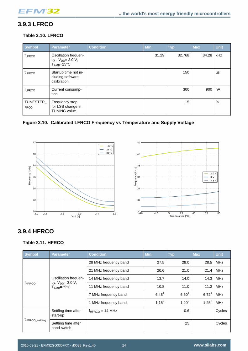
3.9.3 LFRCO
Table 3.10. LFRCO
Symbol Parameter Condition Min Typ Max Unit
fLFRCO Oscillation frequen-cy , VDD= 3.0 V,TAMB=25°C
31.29 32.768 34.28 kHz
tLFRCO Startup time not in-cluding softwarecalibration
150 µs
ILFRCO Current consump-tion
300 900 nA
TUNESTEPL-
FRCO
Frequency stepfor LSB change inTUNING value
1.5 %
Figure 3.10. Calibrated LFRCO Frequency vs Temperature and Supply Voltage
2.0 2.2 2.6 3.0 3.4 3.8Vdd [V]
- 40°C
25°C85°C
30
32
34
36
38
40
42
Freq
uen
cy [
kH
z]
–40 –15 5 25 45 65 85Temperature [°C]
30
32
34
36
38
40
42
Freq
uen
cy [
kH
z]
2.0 V
3 V
3.8 V
3.9.4 HFRCO
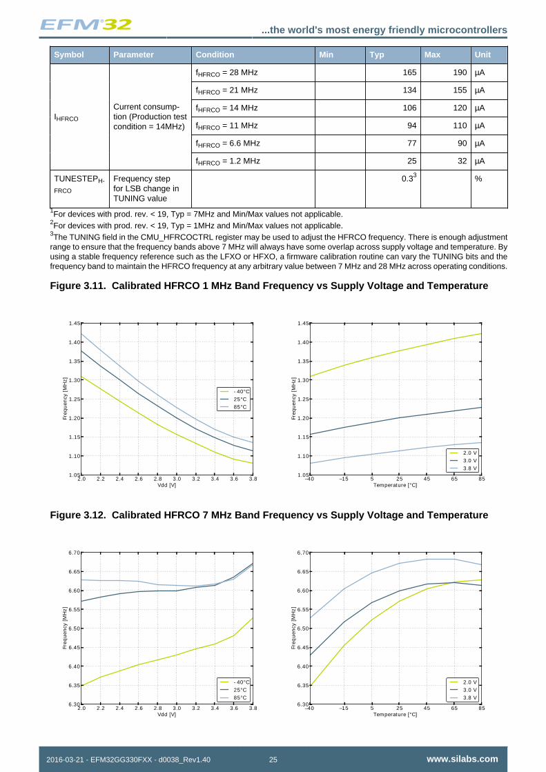
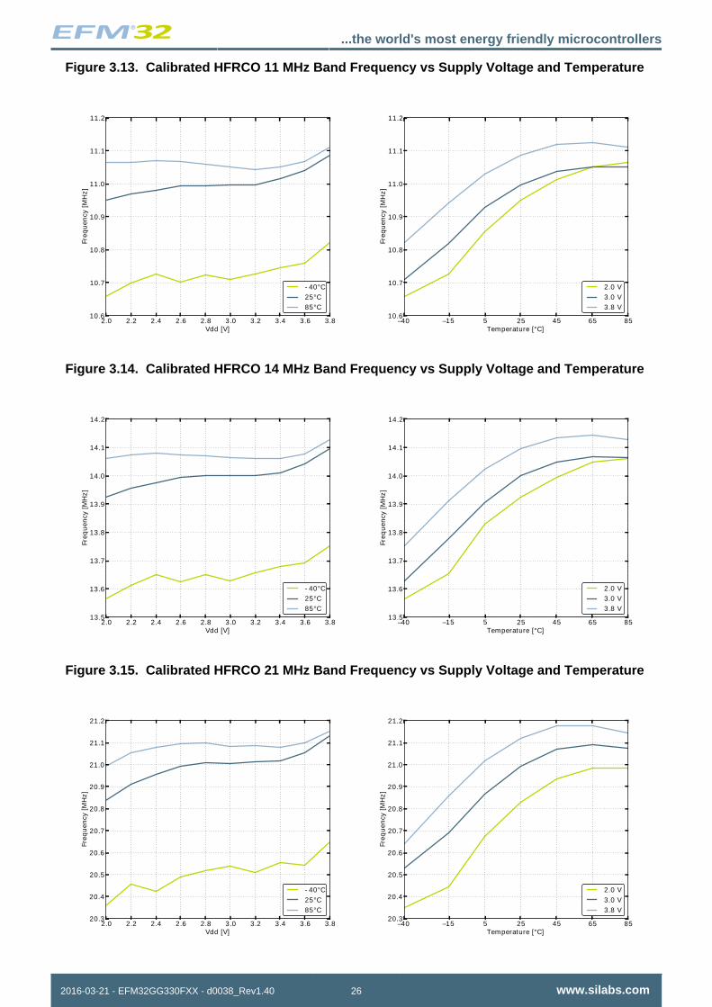
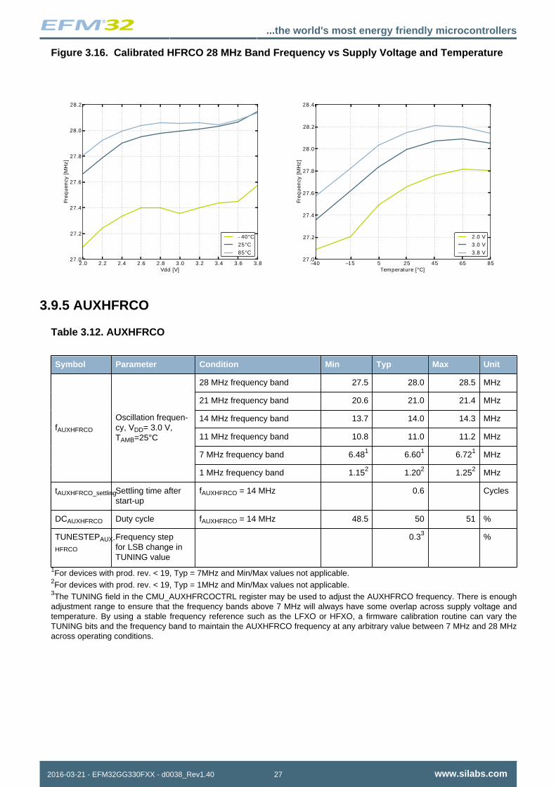
Table 3.11. HFRCO
Symbol Parameter Condition Min Typ Max Unit
28 MHz frequency band 27.5 28.0 28.5 MHz
21 MHz frequency band 20.6 21.0 21.4 MHz
14 MHz frequency band 13.7 14.0 14.3 MHz
11 MHz frequency band 10.8 11.0 11.2 MHz
7 MHz frequency band 6.481 6.601 6.721 MHz
fHFRCO
Oscillation frequen-cy, VDD= 3.0 V,TAMB=25°C
1 MHz frequency band 1.152 1.202 1.252 MHz
Settling time afterstart-up
fHFRCO = 14 MHz 0.6 Cycles
tHFRCO_settlingSettling time afterband switch
25 Cycles
...the world's most energy friendly microcontrollers
2016-03-21 - EFM32GG330FXX - d0038_Rev1.40 25 www.silabs.com
Symbol Parameter Condition Min Typ Max Unit
fHFRCO = 28 MHz 165 190 µA
fHFRCO = 21 MHz 134 155 µA
fHFRCO = 14 MHz 106 120 µA
fHFRCO = 11 MHz 94 110 µA
fHFRCO = 6.6 MHz 77 90 µA
IHFRCO
Current consump-tion (Production testcondition = 14MHz)
fHFRCO = 1.2 MHz 25 32 µA
TUNESTEPH-
FRCO
Frequency stepfor LSB change inTUNING value
0.33 %
1For devices with prod. rev. < 19, Typ = 7MHz and Min/Max values not applicable.2For devices with prod. rev. < 19, Typ = 1MHz and Min/Max values not applicable.3The TUNING field in the CMU_HFRCOCTRL register may be used to adjust the HFRCO frequency. There is enough adjustmentrange to ensure that the frequency bands above 7 MHz will always have some overlap across supply voltage and temperature. Byusing a stable frequency reference such as the LFXO or HFXO, a firmware calibration routine can vary the TUNING bits and thefrequency band to maintain the HFRCO frequency at any arbitrary value between 7 MHz and 28 MHz across operating conditions.
Figure 3.11. Calibrated HFRCO 1 MHz Band Frequency vs Supply Voltage and Temperature
2.0 2.2 2.4 2.6 2.8 3.0 3.2 3.4 3.6 3.8Vdd [V]
1.05
1.10
1.15
1.20
1.25
1.30
1.35
1.40
1.45
Freq
uen
cy [
MH
z]
- 40°C
25°C
85°C
–40 –15 5 25 45 65 85Temperature [°C]
1.05
1.10
1.15
1.20
1.25
1.30
1.35
1.40
1.45
Freq
uen
cy [
MH
z]
2.0 V
3.0 V
3.8 V
Figure 3.12. Calibrated HFRCO 7 MHz Band Frequency vs Supply Voltage and Temperature
2.0 2.2 2.4 2.6 2.8 3.0 3.2 3.4 3.6 3.8Vdd [V]
6.30
6.35
6.40
6.45
6.50
6.55
6.60
6.65
6.70
Freq
uen
cy [
MH
z]
- 40°C
25°C
85°C
–40 –15 5 25 45 65 85Temperature [°C]
6.30
6.35
6.40
6.45
6.50
6.55
6.60
6.65
6.70
Freq
uen
cy [
MH
z]
2.0 V
3.0 V
3.8 V
...the world's most energy friendly microcontrollers
2016-03-21 - EFM32GG330FXX - d0038_Rev1.40 26 www.silabs.com
Figure 3.13. Calibrated HFRCO 11 MHz Band Frequency vs Supply Voltage and Temperature
2.0 2.2 2.4 2.6 2.8 3.0 3.2 3.4 3.6 3.8Vdd [V]
10.6
10.7
10.8
10.9
11.0
11.1
11.2
Freq
uen
cy [
MH
z]
- 40°C
25°C
85°C
–40 –15 5 25 45 65 85Temperature [°C]
10.6
10.7
10.8
10.9
11.0
11.1
11.2
Freq
uen
cy [
MH
z]
2.0 V
3.0 V
3.8 V
Figure 3.14. Calibrated HFRCO 14 MHz Band Frequency vs Supply Voltage and Temperature
2.0 2.2 2.4 2.6 2.8 3.0 3.2 3.4 3.6 3.8Vdd [V]
13.5
13.6
13.7
13.8
13.9
14.0
14.1
14.2
Freq
uen
cy [
MH
z]
- 40°C
25°C
85°C
–40 –15 5 25 45 65 85Temperature [°C]
13.5
13.6
13.7
13.8
13.9
14.0
14.1
14.2
Freq
uen
cy [
MH
z]
2.0 V
3.0 V
3.8 V
Figure 3.15. Calibrated HFRCO 21 MHz Band Frequency vs Supply Voltage and Temperature
2.0 2.2 2.4 2.6 2.8 3.0 3.2 3.4 3.6 3.8Vdd [V]
20.3
20.4
20.5
20.6
20.7
20.8
20.9
21.0
21.1
21.2
Freq
uen
cy [
MH
z]
- 40°C
25°C
85°C
–40 –15 5 25 45 65 85Temperature [°C]
20.3
20.4
20.5
20.6
20.7
20.8
20.9
21.0
21.1
21.2
Freq
uen
cy [
MH
z]
2.0 V
3.0 V
3.8 V
...the world's most energy friendly microcontrollers
2016-03-21 - EFM32GG330FXX - d0038_Rev1.40 27 www.silabs.com
Figure 3.16. Calibrated HFRCO 28 MHz Band Frequency vs Supply Voltage and Temperature
2.0 2.2 2.4 2.6 2.8 3.0 3.2 3.4 3.6 3.8Vdd [V]
27.0
27.2
27.4
27.6
27.8
28.0
28.2
Freq
uen
cy [
MH
z]
- 40°C
25°C
85°C
–40 –15 5 25 45 65 85Temperature [°C]
27.0
27.2
27.4
27.6
27.8
28.0
28.2
28.4
Freq
uen
cy [
MH
z]
2.0 V
3.0 V
3.8 V
3.9.5 AUXHFRCO
Table 3.12. AUXHFRCO
Symbol Parameter Condition Min Typ Max Unit
28 MHz frequency band 27.5 28.0 28.5 MHz
21 MHz frequency band 20.6 21.0 21.4 MHz
14 MHz frequency band 13.7 14.0 14.3 MHz
11 MHz frequency band 10.8 11.0 11.2 MHz
7 MHz frequency band 6.481 6.601 6.721 MHz
fAUXHFRCO
Oscillation frequen-cy, VDD= 3.0 V,TAMB=25°C
1 MHz frequency band 1.152 1.202 1.252 MHz
tAUXHFRCO_settlingSettling time afterstart-up
fAUXHFRCO = 14 MHz 0.6 Cycles
DCAUXHFRCO Duty cycle fAUXHFRCO = 14 MHz 48.5 50 51 %
TUNESTEPAUX-
HFRCO
Frequency stepfor LSB change inTUNING value
0.33 %
1For devices with prod. rev. < 19, Typ = 7MHz and Min/Max values not applicable.2For devices with prod. rev. < 19, Typ = 1MHz and Min/Max values not applicable.3The TUNING field in the CMU_AUXHFRCOCTRL register may be used to adjust the AUXHFRCO frequency. There is enoughadjustment range to ensure that the frequency bands above 7 MHz will always have some overlap across supply voltage andtemperature. By using a stable frequency reference such as the LFXO or HFXO, a firmware calibration routine can vary theTUNING bits and the frequency band to maintain the AUXHFRCO frequency at any arbitrary value between 7 MHz and 28 MHzacross operating conditions.
...the world's most energy friendly microcontrollers
2016-03-21 - EFM32GG330FXX - d0038_Rev1.40 28 www.silabs.com
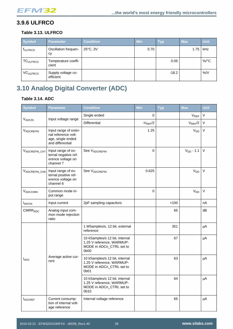
3.9.6 ULFRCO
Table 3.13. ULFRCO
Symbol Parameter Condition Min Typ Max Unit
fULFRCO Oscillation frequen-cy
25°C, 3V 0.70 1.75 kHz
TCULFRCO Temperature coeffi-cient
0.05 %/°C
VCULFRCO Supply voltage co-efficient
-18.2 %/V
3.10 Analog Digital Converter (ADC)
Table 3.14. ADC
Symbol Parameter Condition Min Typ Max Unit
Single ended 0 VREF VVADCIN Input voltage range
Differential -VREF/2 VREF/2 V
VADCREFIN Input range of exter-nal reference volt-age, single endedand differential
1.25 VDD V
VADCREFIN_CH7 Input range of ex-ternal negative ref-erence voltage onchannel 7
See VADCREFIN 0 VDD - 1.1 V
VADCREFIN_CH6 Input range of ex-ternal positive ref-erence voltage onchannel 6
See VADCREFIN 0.625 VDD V
VADCCMIN Common mode in-put range
0 VDD V
IADCIN Input current 2pF sampling capacitors <100 nA
CMRRADC Analog input com-mon mode rejectionratio
65 dB
1 MSamples/s, 12 bit, externalreference
351 µA
10 kSamples/s 12 bit, internal1.25 V reference, WARMUP-MODE in ADCn_CTRL set to0b00
67 µA
10 kSamples/s 12 bit, internal1.25 V reference, WARMUP-MODE in ADCn_CTRL set to0b01
63 µAIADCAverage active cur-rent
10 kSamples/s 12 bit, internal1.25 V reference, WARMUP-MODE in ADCn_CTRL set to0b10
64 µA
IADCREF Current consump-tion of internal volt-age reference
Internal voltage reference 65 µA
...the world's most energy friendly microcontrollers
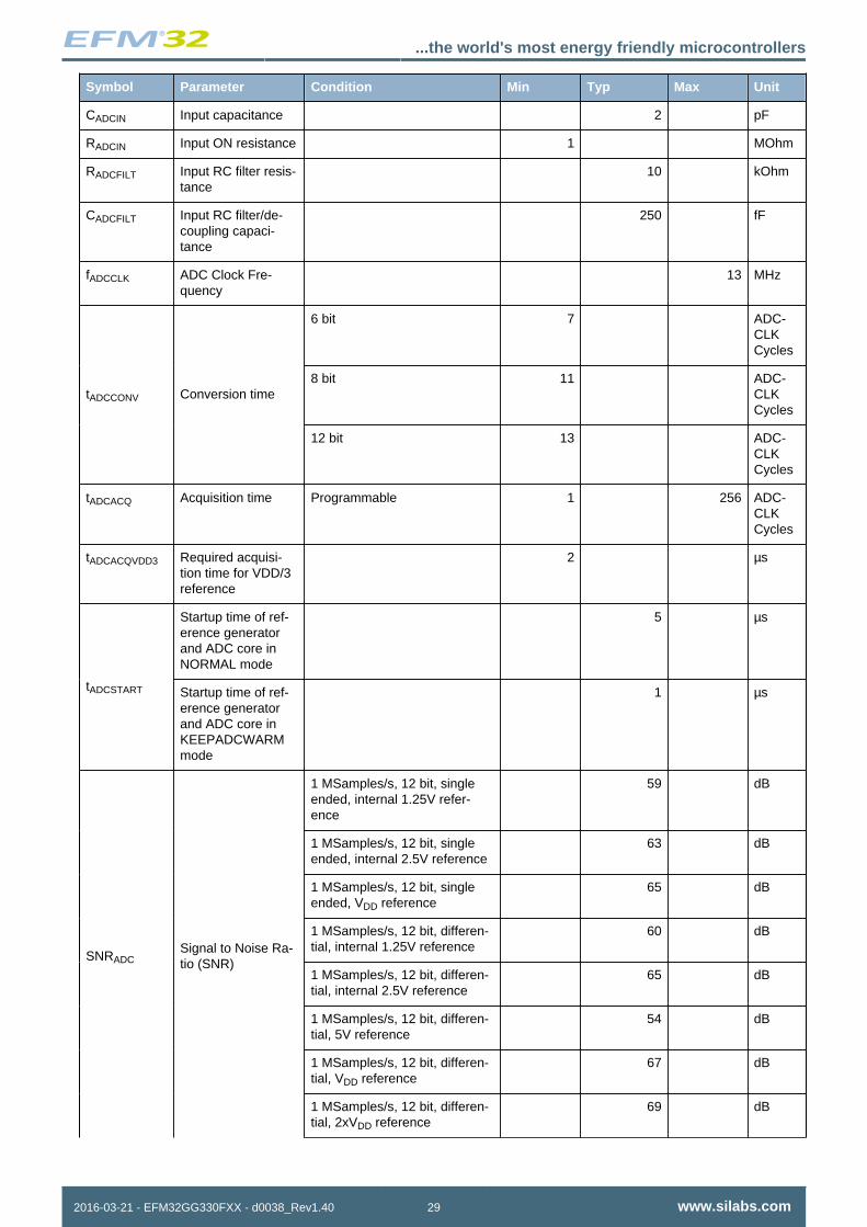
2016-03-21 - EFM32GG330FXX - d0038_Rev1.40 29 www.silabs.com
Symbol Parameter Condition Min Typ Max Unit
CADCIN Input capacitance 2 pF
RADCIN Input ON resistance 1 MOhm
RADCFILT Input RC filter resis-tance
10 kOhm
CADCFILT Input RC filter/de-coupling capaci-tance
250 fF
fADCCLK ADC Clock Fre-quency
13 MHz
6 bit 7 ADC-CLKCycles
8 bit 11 ADC-CLKCycles
tADCCONV Conversion time
12 bit 13 ADC-CLKCycles
tADCACQ Acquisition time Programmable 1 256 ADC-CLKCycles
tADCACQVDD3 Required acquisi-tion time for VDD/3reference
2 µs
Startup time of ref-erence generatorand ADC core inNORMAL mode
5 µs
tADCSTART Startup time of ref-erence generatorand ADC core inKEEPADCWARMmode
1 µs
1 MSamples/s, 12 bit, singleended, internal 1.25V refer-ence
59 dB
1 MSamples/s, 12 bit, singleended, internal 2.5V reference
63 dB
1 MSamples/s, 12 bit, singleended, VDD reference
65 dB
1 MSamples/s, 12 bit, differen-tial, internal 1.25V reference
60 dB
1 MSamples/s, 12 bit, differen-tial, internal 2.5V reference
65 dB
1 MSamples/s, 12 bit, differen-tial, 5V reference
54 dB
1 MSamples/s, 12 bit, differen-tial, VDD reference
67 dB
SNRADCSignal to Noise Ra-tio (SNR)
1 MSamples/s, 12 bit, differen-tial, 2xVDD reference
69 dB
...the world's most energy friendly microcontrollers
2016-03-21 - EFM32GG330FXX - d0038_Rev1.40 30 www.silabs.com
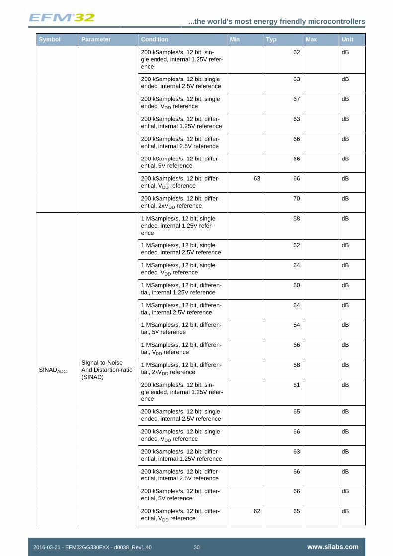
Symbol Parameter Condition Min Typ Max Unit
200 kSamples/s, 12 bit, sin-gle ended, internal 1.25V refer-ence
62 dB
200 kSamples/s, 12 bit, singleended, internal 2.5V reference
63 dB
200 kSamples/s, 12 bit, singleended, VDD reference
67 dB
200 kSamples/s, 12 bit, differ-ential, internal 1.25V reference
63 dB
200 kSamples/s, 12 bit, differ-ential, internal 2.5V reference
66 dB
200 kSamples/s, 12 bit, differ-ential, 5V reference
66 dB
200 kSamples/s, 12 bit, differ-ential, VDD reference
63 66 dB
200 kSamples/s, 12 bit, differ-ential, 2xVDD reference
70 dB
1 MSamples/s, 12 bit, singleended, internal 1.25V refer-ence
58 dB
1 MSamples/s, 12 bit, singleended, internal 2.5V reference
62 dB
1 MSamples/s, 12 bit, singleended, VDD reference
64 dB
1 MSamples/s, 12 bit, differen-tial, internal 1.25V reference
60 dB
1 MSamples/s, 12 bit, differen-tial, internal 2.5V reference
64 dB
1 MSamples/s, 12 bit, differen-tial, 5V reference
54 dB
1 MSamples/s, 12 bit, differen-tial, VDD reference
66 dB
1 MSamples/s, 12 bit, differen-tial, 2xVDD reference
68 dB
200 kSamples/s, 12 bit, sin-gle ended, internal 1.25V refer-ence
61 dB
200 kSamples/s, 12 bit, singleended, internal 2.5V reference
65 dB
200 kSamples/s, 12 bit, singleended, VDD reference
66 dB
200 kSamples/s, 12 bit, differ-ential, internal 1.25V reference
63 dB
200 kSamples/s, 12 bit, differ-ential, internal 2.5V reference
66 dB
200 kSamples/s, 12 bit, differ-ential, 5V reference
66 dB
SINADADC
SIgnal-to-NoiseAnd Distortion-ratio(SINAD)
200 kSamples/s, 12 bit, differ-ential, VDD reference
62 65 dB
...the world's most energy friendly microcontrollers
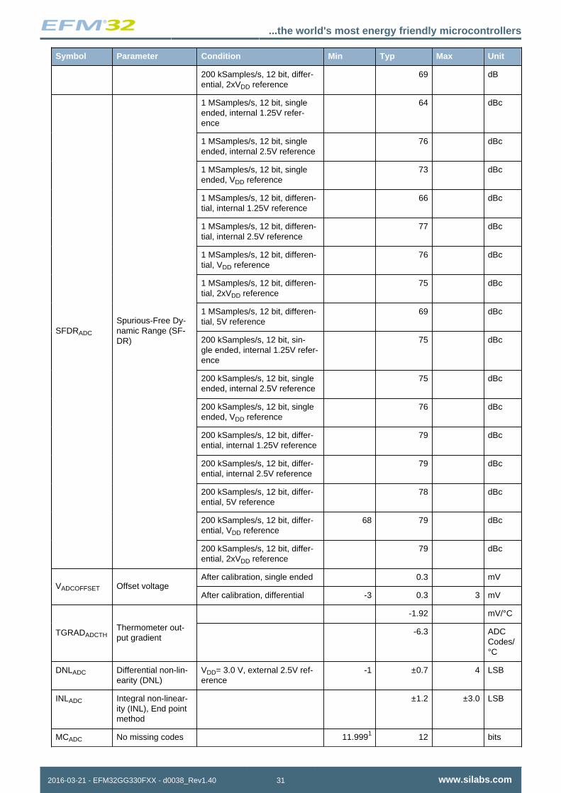
2016-03-21 - EFM32GG330FXX - d0038_Rev1.40 31 www.silabs.com
Symbol Parameter Condition Min Typ Max Unit
200 kSamples/s, 12 bit, differ-ential, 2xVDD reference
69 dB
1 MSamples/s, 12 bit, singleended, internal 1.25V refer-ence
64 dBc
1 MSamples/s, 12 bit, singleended, internal 2.5V reference
76 dBc
1 MSamples/s, 12 bit, singleended, VDD reference
73 dBc
1 MSamples/s, 12 bit, differen-tial, internal 1.25V reference
66 dBc
1 MSamples/s, 12 bit, differen-tial, internal 2.5V reference
77 dBc
1 MSamples/s, 12 bit, differen-tial, VDD reference
76 dBc
1 MSamples/s, 12 bit, differen-tial, 2xVDD reference
75 dBc
1 MSamples/s, 12 bit, differen-tial, 5V reference
69 dBc
200 kSamples/s, 12 bit, sin-gle ended, internal 1.25V refer-ence
75 dBc
200 kSamples/s, 12 bit, singleended, internal 2.5V reference
75 dBc
200 kSamples/s, 12 bit, singleended, VDD reference
76 dBc
200 kSamples/s, 12 bit, differ-ential, internal 1.25V reference
79 dBc
200 kSamples/s, 12 bit, differ-ential, internal 2.5V reference
79 dBc
200 kSamples/s, 12 bit, differ-ential, 5V reference
78 dBc
200 kSamples/s, 12 bit, differ-ential, VDD reference
68 79 dBc
SFDRADC
Spurious-Free Dy-namic Range (SF-DR)
200 kSamples/s, 12 bit, differ-ential, 2xVDD reference
79 dBc
After calibration, single ended 0.3 mVVADCOFFSET Offset voltage
After calibration, differential -3 0.3 3 mV
-1.92 mV/°C
TGRADADCTHThermometer out-put gradient
-6.3 ADCCodes/°C
DNLADC Differential non-lin-earity (DNL)
VDD= 3.0 V, external 2.5V ref-erence
-1 ±0.7 4 LSB
INLADC Integral non-linear-ity (INL), End pointmethod
±1.2 ±3.0 LSB
MCADC No missing codes 11.9991 12 bits
...the world's most energy friendly microcontrollers
2016-03-21 - EFM32GG330FXX - d0038_Rev1.40 32 www.silabs.com
Symbol Parameter Condition Min Typ Max Unit
1.25V reference 0.012 0.0333 %/°CGAINED Gain error drift
2.5V reference 0.012 0.033 %/°C
1.25V reference 0.22 0.73 LSB/°COFFSETED Offset error drift
2.5V reference 0.22 0.623 LSB/°C1On the average every ADC will have one missing code, most likely to appear around 2048 +/- n*512 where n can be a value inthe set {-3, -2, -1, 1, 2, 3}. There will be no missing code around 2048, and in spite of the missing code the ADC will be monotonicat all times so that a response to a slowly increasing input will always be a slowly increasing output. Around the one code that ismissing, the neighbour codes will look wider in the DNL plot. The spectra will show spurs on the level of -78dBc for a full scaleinput for chips that have the missing code issue.2Typical numbers given by abs(Mean) / (85 - 25).3Max number given by (abs(Mean) + 3x stddev) / (85 - 25).
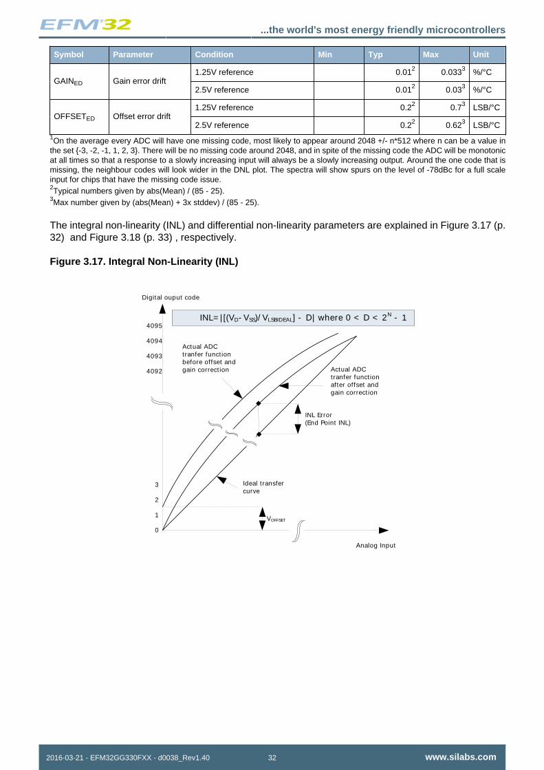
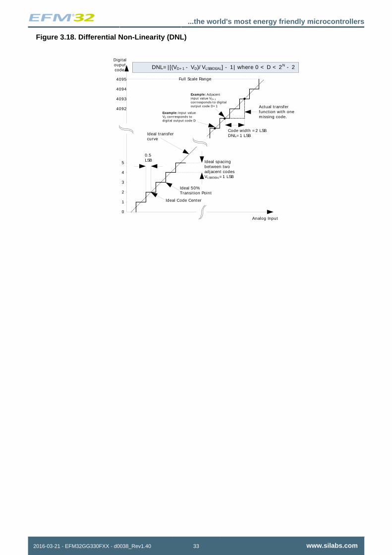
The integral non-linearity (INL) and differential non-linearity parameters are explained in Figure 3.17 (p.32) and Figure 3.18 (p. 33) , respectively.
Figure 3.17. Integral Non-Linearity (INL)
Ideal t ransfer curve
Digital ouput code
Analog Input
INL= | [(VD- VSS)/ VLSBIDEAL] - D| where 0 < D < 2N - 1
0
1
2
3
4092
4093
4094
4095
VOFFSET
Actual ADC tranfer funct ion before offset and gain correct ion Actual ADC
tranfer funct ion after offset and gain correct ion
INL Error (End Point INL)
...the world's most energy friendly microcontrollers
2016-03-21 - EFM32GG330FXX - d0038_Rev1.40 33 www.silabs.com
Figure 3.18. Differential Non-Linearity (DNL)
Ideal t ransfer curve
Digital ouputcode
Analog Input
DNL= | [(VD+ 1 - VD)/ VLSBIDEAL] - 1| where 0 < D < 2N - 2
0
1
2
3
4092
4093
4094
4095
Actual t ransfer funct ion with one missing code.
4
5
Full Scale Range
0.5 LSB
Ideal Code Center
Ideal 50% Transit ion Point
Ideal spacing between two adjacent codesVLSBIDEAL= 1 LSB
Code width = 2 LSBDNL= 1 LSB
Example: Adjacent input value VD+ 1 corrresponds to digital output code D+ 1
Example: Input value VD corrresponds to digital output code D
...the world's most energy friendly microcontrollers
2016-03-21 - EFM32GG330FXX - d0038_Rev1.40 34 www.silabs.com
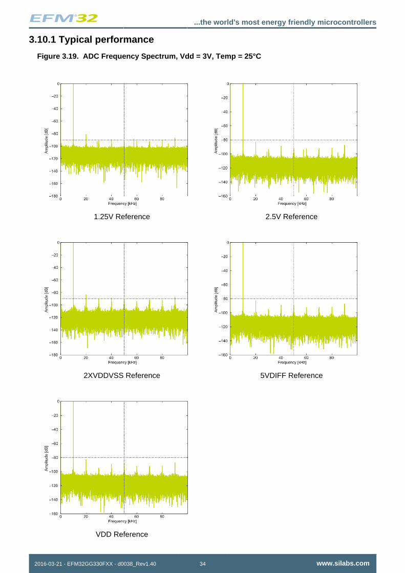
3.10.1 Typical performance
Figure 3.19. ADC Frequency Spectrum, Vdd = 3V, Temp = 25°C
1.25V Reference 2.5V Reference
2XVDDVSS Reference 5VDIFF Reference
VDD Reference
...the world's most energy friendly microcontrollers
2016-03-21 - EFM32GG330FXX - d0038_Rev1.40 35 www.silabs.com
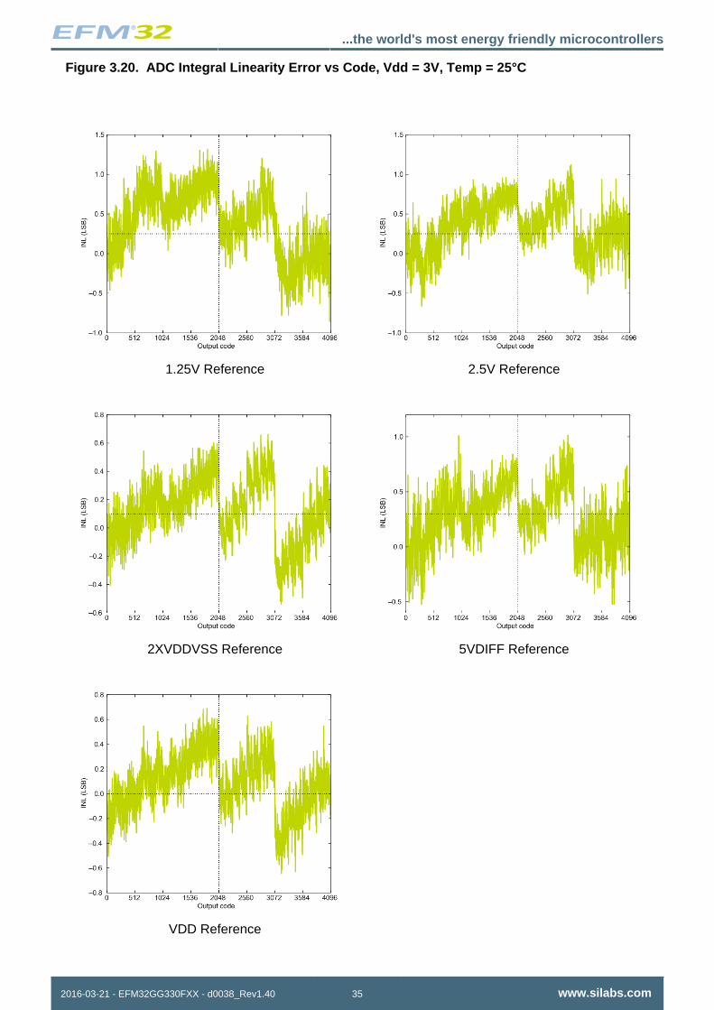
Figure 3.20. ADC Integral Linearity Error vs Code, Vdd = 3V, Temp = 25°C
1.25V Reference 2.5V Reference
2XVDDVSS Reference 5VDIFF Reference
VDD Reference
...the world's most energy friendly microcontrollers
2016-03-21 - EFM32GG330FXX - d0038_Rev1.40 36 www.silabs.com
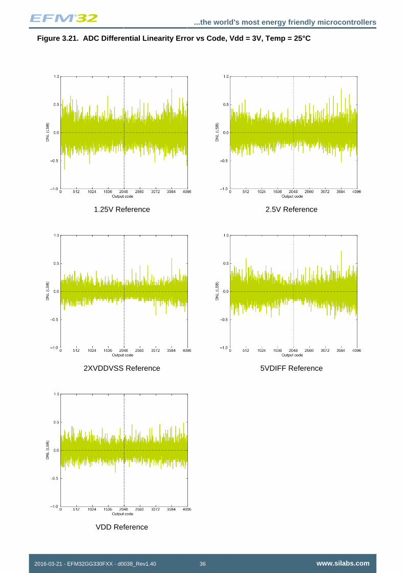
Figure 3.21. ADC Differential Linearity Error vs Code, Vdd = 3V, Temp = 25°C
1.25V Reference 2.5V Reference
2XVDDVSS Reference 5VDIFF Reference
VDD Reference
...the world's most energy friendly microcontrollers
2016-03-21 - EFM32GG330FXX - d0038_Rev1.40 37 www.silabs.com
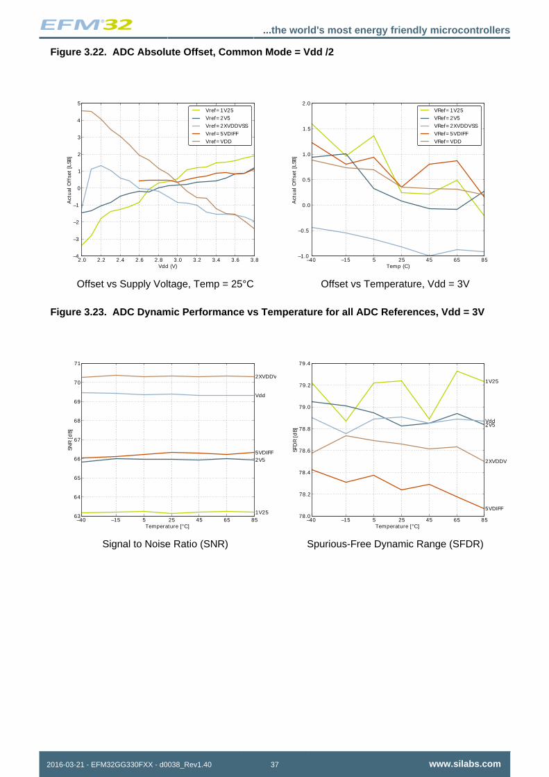
Figure 3.22. ADC Absolute Offset, Common Mode = Vdd /2
2.0 2.2 2.4 2.6 2.8 3.0 3.2 3.4 3.6 3.8Vdd (V)
–4
–3
–2
–1
0
1
2
3
4
5
Act
ual
Off
set
[LSB
]
Vref= 1V25
Vref= 2V5
Vref= 2XVDDVSS
Vref= 5VDIFF
Vref= VDD
Offset vs Supply Voltage, Temp = 25°C
–40 –15 5 25 45 65 85Temp (C)
–1.0
–0.5
0.0
0.5
1.0
1.5
2.0
Act
ual
Off
set
[LSB
]
VRef= 1V25
VRef= 2V5
VRef= 2XVDDVSS
VRef= 5VDIFF
VRef= VDD
Offset vs Temperature, Vdd = 3V
Figure 3.23. ADC Dynamic Performance vs Temperature for all ADC References, Vdd = 3V
–40 –15 5 25 45 65 85Temperature [°C]
63
64
65
66
67
68
69
70
71
SNR
[d
B]
1V25
2V5
Vdd
5VDIFF
2XVDDVSS
Signal to Noise Ratio (SNR)
–40 –15 5 25 45 65 85Temperature [°C]
78.0
78.2
78.4
78.6
78.8
79.0
79.2
79.4
SFD
R [
dB]
1V25
2V5Vdd
5VDIFF
2XVDDVSS
Spurious-Free Dynamic Range (SFDR)
...the world's most energy friendly microcontrollers
2016-03-21 - EFM32GG330FXX - d0038_Rev1.40 38 www.silabs.com
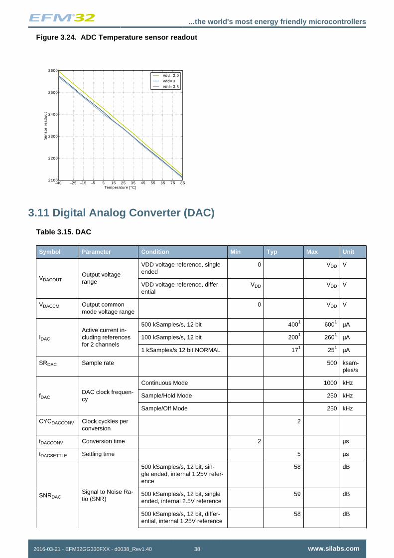
Figure 3.24. ADC Temperature sensor readout
–40 –25 –15 –5 5 15 25 35 45 55 65 75 85Temperature [°C]
2100
2200
2300
2400
2500
2600
Sen
sor
read
ou
t
Vdd= 2.0
Vdd= 3
Vdd= 3.8
3.11 Digital Analog Converter (DAC)
Table 3.15. DAC
Symbol Parameter Condition Min Typ Max Unit
VDD voltage reference, singleended
0 VDD V
VDACOUTOutput voltagerange VDD voltage reference, differ-
ential-VDD VDD V
VDACCM Output commonmode voltage range
0 VDD V
500 kSamples/s, 12 bit 4001 6001 µA
100 kSamples/s, 12 bit 2001 2601 µAIDAC
Active current in-cluding referencesfor 2 channels
1 kSamples/s 12 bit NORMAL 171 251 µA
SRDAC Sample rate 500 ksam-ples/s
Continuous Mode 1000 kHz
Sample/Hold Mode 250 kHzfDACDAC clock frequen-cy
Sample/Off Mode 250 kHz
CYCDACCONV Clock cyckles perconversion
2
tDACCONV Conversion time 2 µs
tDACSETTLE Settling time 5 µs
500 kSamples/s, 12 bit, sin-gle ended, internal 1.25V refer-ence
58 dB
500 kSamples/s, 12 bit, singleended, internal 2.5V reference
59 dBSNRDACSignal to Noise Ra-tio (SNR)
500 kSamples/s, 12 bit, differ-ential, internal 1.25V reference
58 dB
...the world's most energy friendly microcontrollers
2016-03-21 - EFM32GG330FXX - d0038_Rev1.40 39 www.silabs.com
Symbol Parameter Condition Min Typ Max Unit
500 kSamples/s, 12 bit, differ-ential, internal 2.5V reference
58 dB
500 kSamples/s, 12 bit, differ-ential, VDD reference
59 dB
500 kSamples/s, 12 bit, sin-gle ended, internal 1.25V refer-ence
57 dB
500 kSamples/s, 12 bit, singleended, internal 2.5V reference
54 dB
500 kSamples/s, 12 bit, differ-ential, internal 1.25V reference
56 dB
500 kSamples/s, 12 bit, differ-ential, internal 2.5V reference
53 dB
SNDRDAC
Signal to Noise-pulse Distortion Ra-tio (SNDR)
500 kSamples/s, 12 bit, differ-ential, VDD reference
55 dB
500 kSamples/s, 12 bit, sin-gle ended, internal 1.25V refer-ence
62 dBc
500 kSamples/s, 12 bit, singleended, internal 2.5V reference
56 dBc
500 kSamples/s, 12 bit, differ-ential, internal 1.25V reference
61 dBc
500 kSamples/s, 12 bit, differ-ential, internal 2.5V reference
55 dBc
SFDRDAC
Spurious-FreeDynamicRange(SFDR)
500 kSamples/s, 12 bit, differ-ential, VDD reference
60 dBc
After calibration, single ended 2 12 mVVDACOFFSET Offset voltage
After calibration, differential 2 mV
DNLDAC Differential non-lin-earity
±1 LSB
INLDAC Integral non-lineari-ty
±5 LSB
MCDAC No missing codes 12 bits1Measured with a static input code and no loading on the output.
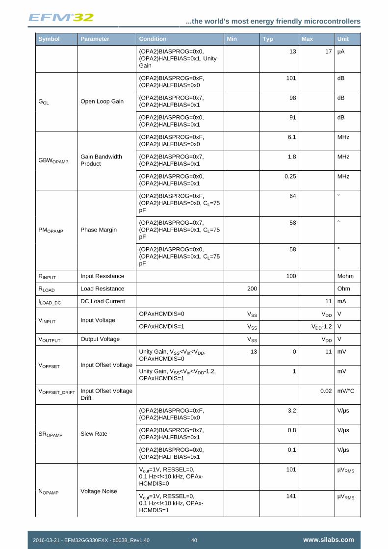
3.12 Operational Amplifier (OPAMP)
The electrical characteristics for the Operational Amplifiers are based on simulations.
Table 3.16. OPAMP
Symbol Parameter Condition Min Typ Max Unit
(OPA2)BIASPROG=0xF,(OPA2)HALFBIAS=0x0, UnityGain
350 405 µA
IOPAMP Active Current(OPA2)BIASPROG=0x7,(OPA2)HALFBIAS=0x1, UnityGain
95 115 µA
...the world's most energy friendly microcontrollers
2016-03-21 - EFM32GG330FXX - d0038_Rev1.40 40 www.silabs.com
Symbol Parameter Condition Min Typ Max Unit
(OPA2)BIASPROG=0x0,(OPA2)HALFBIAS=0x1, UnityGain
13 17 µA
(OPA2)BIASPROG=0xF,(OPA2)HALFBIAS=0x0
101 dB
(OPA2)BIASPROG=0x7,(OPA2)HALFBIAS=0x1
98 dBGOL Open Loop Gain
(OPA2)BIASPROG=0x0,(OPA2)HALFBIAS=0x1
91 dB
(OPA2)BIASPROG=0xF,(OPA2)HALFBIAS=0x0
6.1 MHz
(OPA2)BIASPROG=0x7,(OPA2)HALFBIAS=0x1
1.8 MHzGBWOPAMP
Gain BandwidthProduct
(OPA2)BIASPROG=0x0,(OPA2)HALFBIAS=0x1
0.25 MHz
(OPA2)BIASPROG=0xF,(OPA2)HALFBIAS=0x0, CL=75pF
64 °
(OPA2)BIASPROG=0x7,(OPA2)HALFBIAS=0x1, CL=75pF
58 °PMOPAMP Phase Margin
(OPA2)BIASPROG=0x0,(OPA2)HALFBIAS=0x1, CL=75pF
58 °
RINPUT Input Resistance 100 Mohm
RLOAD Load Resistance 200 Ohm
ILOAD_DC DC Load Current 11 mA
OPAxHCMDIS=0 VSS VDD VVINPUT Input Voltage
OPAxHCMDIS=1 VSS VDD-1.2 V
VOUTPUT Output Voltage VSS VDD V
Unity Gain, VSS<Vin<VDD,OPAxHCMDIS=0
-13 0 11 mV
VOFFSET Input Offset VoltageUnity Gain, VSS<Vin<VDD-1.2,OPAxHCMDIS=1
1 mV
VOFFSET_DRIFT Input Offset VoltageDrift
0.02 mV/°C
(OPA2)BIASPROG=0xF,(OPA2)HALFBIAS=0x0
3.2 V/µs
(OPA2)BIASPROG=0x7,(OPA2)HALFBIAS=0x1
0.8 V/µsSROPAMP Slew Rate
(OPA2)BIASPROG=0x0,(OPA2)HALFBIAS=0x1
0.1 V/µs
Vout=1V, RESSEL=0,0.1 Hz<f<10 kHz, OPAx-HCMDIS=0
101 µVRMS
NOPAMP Voltage NoiseVout=1V, RESSEL=0,0.1 Hz<f<10 kHz, OPAx-HCMDIS=1
141 µVRMS
...the world's most energy friendly microcontrollers
2016-03-21 - EFM32GG330FXX - d0038_Rev1.40 41 www.silabs.com
Symbol Parameter Condition Min Typ Max Unit
Vout=1V, RESSEL=0, 0.1Hz<f<1 MHz, OPAxHCMDIS=0
196 µVRMS
Vout=1V, RESSEL=0, 0.1Hz<f<1 MHz, OPAxHCMDIS=1
229 µVRMS
RESSEL=7, 0.1 Hz<f<10 kHz,OPAxHCMDIS=0
1230 µVRMS
RESSEL=7, 0.1 Hz<f<10 kHz,OPAxHCMDIS=1
2130 µVRMS
RESSEL=7, 0.1 Hz<f<1 MHz,OPAxHCMDIS=0
1630 µVRMS
RESSEL=7, 0.1 Hz<f<1 MHz,OPAxHCMDIS=1
2590 µVRMS
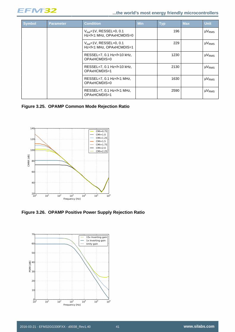
Figure 3.25. OPAMP Common Mode Rejection Ratio
Figure 3.26. OPAMP Positive Power Supply Rejection Ratio
...the world's most energy friendly microcontrollers
2016-03-21 - EFM32GG330FXX - d0038_Rev1.40 42 www.silabs.com
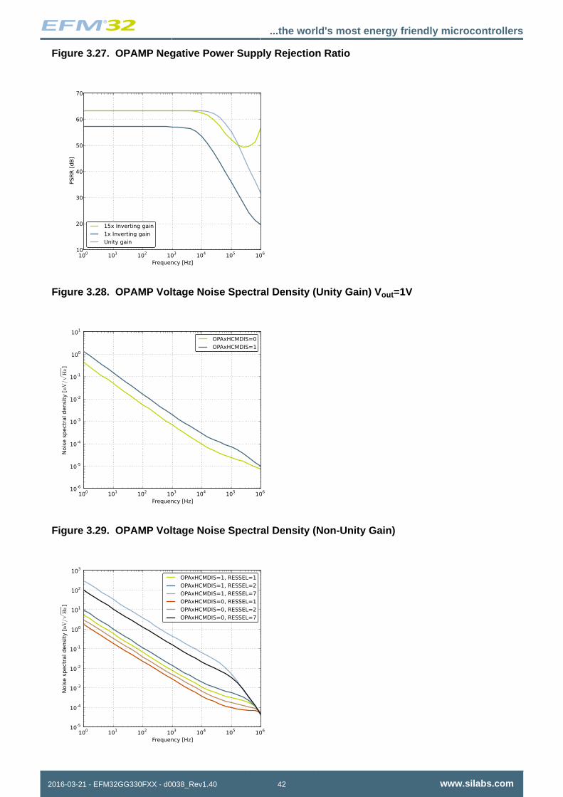
Figure 3.27. OPAMP Negative Power Supply Rejection Ratio
Figure 3.28. OPAMP Voltage Noise Spectral Density (Unity Gain) Vout=1V
Figure 3.29. OPAMP Voltage Noise Spectral Density (Non-Unity Gain)
...the world's most energy friendly microcontrollers
2016-03-21 - EFM32GG330FXX - d0038_Rev1.40 43 www.silabs.com
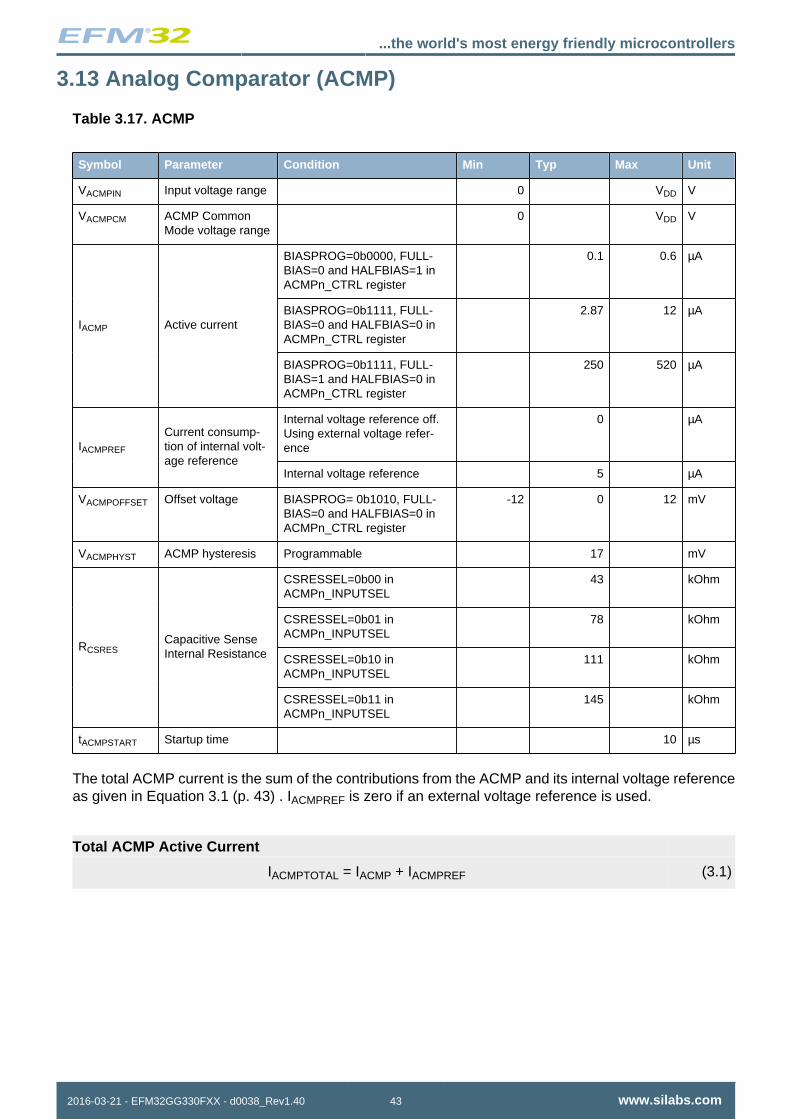
3.13 Analog Comparator (ACMP)
Table 3.17. ACMP
Symbol Parameter Condition Min Typ Max Unit
VACMPIN Input voltage range 0 VDD V
VACMPCM ACMP CommonMode voltage range
0 VDD V
BIASPROG=0b0000, FULL-BIAS=0 and HALFBIAS=1 inACMPn_CTRL register
0.1 0.6 µA
BIASPROG=0b1111, FULL-BIAS=0 and HALFBIAS=0 inACMPn_CTRL register
2.87 12 µAIACMP Active current
BIASPROG=0b1111, FULL-BIAS=1 and HALFBIAS=0 inACMPn_CTRL register
250 520 µA
Internal voltage reference off.Using external voltage refer-ence
0 µA
IACMPREF
Current consump-tion of internal volt-age reference
Internal voltage reference 5 µA
VACMPOFFSET Offset voltage BIASPROG= 0b1010, FULL-BIAS=0 and HALFBIAS=0 inACMPn_CTRL register
-12 0 12 mV
VACMPHYST ACMP hysteresis Programmable 17 mV
CSRESSEL=0b00 inACMPn_INPUTSEL
43 kOhm
CSRESSEL=0b01 inACMPn_INPUTSEL
78 kOhm
CSRESSEL=0b10 inACMPn_INPUTSEL
111 kOhmRCSRES
Capacitive SenseInternal Resistance
CSRESSEL=0b11 inACMPn_INPUTSEL
145 kOhm
tACMPSTART Startup time 10 µs
The total ACMP current is the sum of the contributions from the ACMP and its internal voltage referenceas given in Equation 3.1 (p. 43) . IACMPREF is zero if an external voltage reference is used.
Total ACMP Active Current
IACMPTOTAL = IACMP + IACMPREF (3.1)
...the world's most energy friendly microcontrollers
2016-03-21 - EFM32GG330FXX - d0038_Rev1.40 44 www.silabs.com
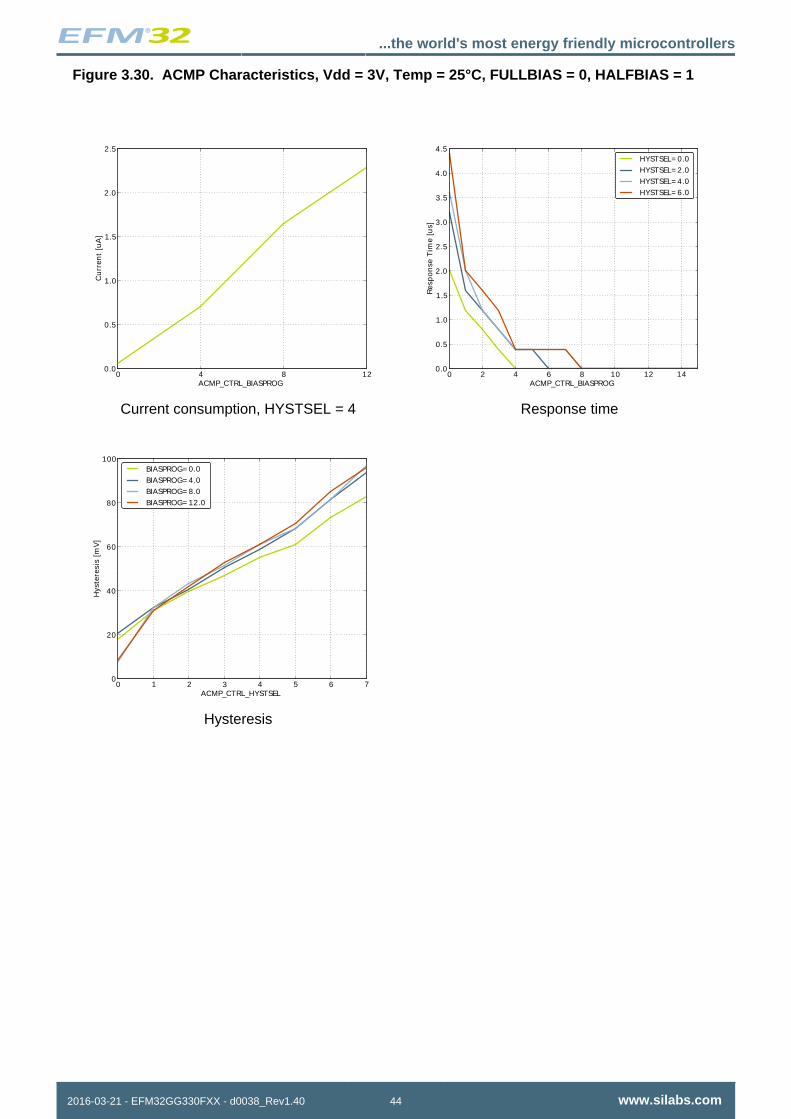
Figure 3.30. ACMP Characteristics, Vdd = 3V, Temp = 25°C, FULLBIAS = 0, HALFBIAS = 1
0 4 8 12ACMP_CTRL_BIASPROG
0.0
0.5
1.0
1.5
2.0
2.5
Cu
rren
t [u
A]
Current consumption, HYSTSEL = 4
0 2 4 6 8 10 12 14ACMP_CTRL_BIASPROG
0.0
0.5
1.0
1.5
2.0
2.5
3.0
3.5
4.0
4.5
Res
po
nse
Tim
e [u
s]
HYSTSEL= 0.0
HYSTSEL= 2.0
HYSTSEL= 4.0
HYSTSEL= 6.0
Response time
0 1 2 3 4 5 6 7ACMP_CTRL_HYSTSEL
0
20
40
60
80
100
Hys
tere
sis
[mV
]
BIASPROG= 0.0
BIASPROG= 4.0
BIASPROG= 8.0
BIASPROG= 12.0
Hysteresis
...the world's most energy friendly microcontrollers
2016-03-21 - EFM32GG330FXX - d0038_Rev1.40 45 www.silabs.com
3.14 Voltage Comparator (VCMP)
Table 3.18. VCMP
Symbol Parameter Condition Min Typ Max Unit
VVCMPIN Input voltage range VDD V
VVCMPCM VCMP CommonMode voltage range
VDD V
BIASPROG=0b0000 andHALFBIAS=1 in VCMPn_CTRLregister
0.3 0.6 µA
IVCMP Active currentBIASPROG=0b1111 andHALFBIAS=0 in VCMPn_CTRLregister. LPREF=0.
22 30 µA
tVCMPREF Startup time refer-ence generator
NORMAL 10 µs
Single ended -230 -40 190 mVVVCMPOFFSET Offset voltage
Differential 10 mV
VVCMPHYST VCMP hysteresis 40 mV
tVCMPSTART Startup time 10 µs
The VDD trigger level can be configured by setting the TRIGLEVEL field of the VCMP_CTRL register inaccordance with the following equation:
VCMP Trigger Level as a Function of Level Setting
VDD Trigger Level=1.667V+0.034 ×TRIGLEVEL (3.2)
3.15 I2C
Table 3.19. I2C Standard-mode (Sm)
Symbol Parameter Min Typ Max Unit
fSCL SCL clock frequency 0 1001 kHz
tLOW SCL clock low time 4.7 µs
tHIGH SCL clock high time 4.0 µs
tSU,DAT SDA set-up time 250 ns
tHD,DAT SDA hold time 8 34502,3 ns
tSU,STA Repeated START condition set-up time 4.7 µs
tHD,STA (Repeated) START condition hold time 4.0 µs
tSU,STO STOP condition set-up time 4.0 µs
tBUF Bus free time between a STOP and START condition 4.7 µs1For the minimum HFPERCLK frequency required in Standard-mode, see the I2C chapter in the EFM32GG Reference Manual.2The maximum SDA hold time (tHD,DAT) needs to be met only when the device does not stretch the low time of SCL (tLOW).3When transmitting data, this number is guaranteed only when I2Cn_CLKDIV < ((3450*10-9 [s] * fHFPERCLK [Hz]) - 4).
...the world's most energy friendly microcontrollers
2016-03-21 - EFM32GG330FXX - d0038_Rev1.40 46 www.silabs.com
Table 3.20. I2C Fast-mode (Fm)
Symbol Parameter Min Typ Max Unit
fSCL SCL clock frequency 0 4001 kHz
tLOW SCL clock low time 1.3 µs
tHIGH SCL clock high time 0.6 µs
tSU,DAT SDA set-up time 100 ns
tHD,DAT SDA hold time 8 9002,3 ns
tSU,STA Repeated START condition set-up time 0.6 µs
tHD,STA (Repeated) START condition hold time 0.6 µs
tSU,STO STOP condition set-up time 0.6 µs
tBUF Bus free time between a STOP and START condition 1.3 µs1For the minimum HFPERCLK frequency required in Fast-mode, see the I2C chapter in the EFM32GG Reference Manual.2The maximum SDA hold time (tHD,DAT) needs to be met only when the device does not stretch the low time of SCL (tLOW).3When transmitting data, this number is guaranteed only when I2Cn_CLKDIV < ((900*10-9 [s] * fHFPERCLK [Hz]) - 4).
Table 3.21. I2C Fast-mode Plus (Fm+)
Symbol Parameter Min Typ Max Unit
fSCL SCL clock frequency 0 10001 kHz
tLOW SCL clock low time 0.5 µs
tHIGH SCL clock high time 0.26 µs
tSU,DAT SDA set-up time 50 ns
tHD,DAT SDA hold time 8 ns
tSU,STA Repeated START condition set-up time 0.26 µs
tHD,STA (Repeated) START condition hold time 0.26 µs
tSU,STO STOP condition set-up time 0.26 µs
tBUF Bus free time between a STOP and START condition 0.5 µs1For the minimum HFPERCLK frequency required in Fast-mode Plus, see the I2C chapter in the EFM32GG Reference Manual.
3.16 USART SPI
Figure 3.31. SPI Master Timing
CS
SCLKCLKPOL = 0
MOSI
MISO
tCS_MO
tH_MItSU_MI
tSCKL_MO
tSCLK
SCLKCLKPOL = 1
...the world's most energy friendly microcontrollers
2016-03-21 - EFM32GG330FXX - d0038_Rev1.40 47 www.silabs.com
Table 3.22. SPI Master Timing
Symbol Parameter Condition Min Typ Max Unit
tSCLK 1 2 SCLK period 2 * tHFPER-
CLK
ns
tCS_MO 1 2 CS to MOSI -2.00 1.00 ns
tSCLK_MO 1 2 SCLK to MOSI -4.00 3.00 ns
IOVDD = 1.98 V 36.00 nstSU_MI 1 2 MISO setup time
IOVDD = 3.0 V 29.00 ns
tH_MI 1 2 MISO hold time -4.00 ns1Applies for both CLKPHA = 0 and CLKPHA = 1 (figure only shows CLKPHA = 0)2Measurement done at 10% and 90% of VDD (figure shows 50% of VDD)
Figure 3.32. SPI Slave Timing
CS
SCLKCLKPOL = 0
MOSI
MISO
tCS_ACT_MI
tSCLK_HI
tSCLKtSU_MO
tH_MO
tSCLK_MI
tCS_DIS_MI
tSCLK_LO
SCLKCLKPOL = 1
Table 3.23. SPI Slave Timing
Symbol Parameter Min Typ Max Unit
tSCLK_sl 1 2 SCKL period 2 * tHFPER-
CLK
ns
tSCLK_hi 1 2 SCLK high period 3 * tHFPER-
CLK
ns
tSCLK_lo 1 2 SCLK low period 3 * tHFPER-
CLK
ns
tCS_ACT_MI 1 2 CS active to MISO 4.00 30.00 ns
tCS_DIS_MI 1 2 CS disable to MISO 4.00 30.00 ns
tSU_MO 1 2 MOSI setup time 4.00 ns
tH_MO 1 2 MOSI hold time 2 + 2* tHF-
PERCLK
ns
tSCLK_MI 1 2 SCLK to MISO 9 + tHFPER-
CLK
36 + 2*tHF-
PERCLK
ns
1Applies for both CLKPHA = 0 and CLKPHA = 1 (figure only shows CLKPHA = 0)2Measurement done at 10% and 90% of VDD (figure shows 50% of VDD)
3.17 USBThe USB hardware in the EFM32GG330 passes all tests for USB 2.0 Full Speed certification. See thetest-report distributed with application note "AN0046 - USB Hardware Design Guide".
...the world's most energy friendly microcontrollers
2016-03-21 - EFM32GG330FXX - d0038_Rev1.40 48 www.silabs.com
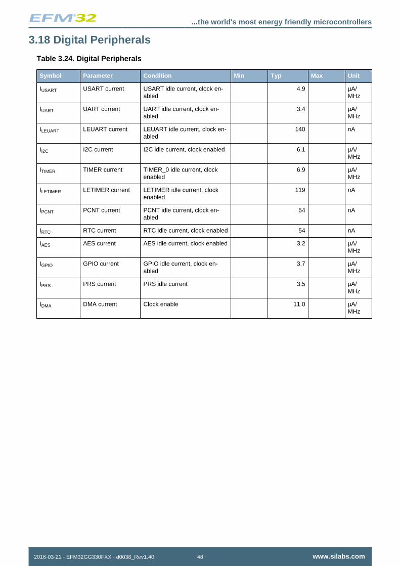
3.18 Digital Peripherals
Table 3.24. Digital Peripherals
Symbol Parameter Condition Min Typ Max Unit
IUSART USART current USART idle current, clock en-abled
4.9 µA/MHz
IUART UART current UART idle current, clock en-abled
3.4 µA/MHz
ILEUART LEUART current LEUART idle current, clock en-abled
140 nA
II2C I2C current I2C idle current, clock enabled 6.1 µA/MHz
ITIMER TIMER current TIMER_0 idle current, clockenabled
6.9 µA/MHz
ILETIMER LETIMER current LETIMER idle current, clockenabled
119 nA
IPCNT PCNT current PCNT idle current, clock en-abled
54 nA
IRTC RTC current RTC idle current, clock enabled 54 nA
IAES AES current AES idle current, clock enabled 3.2 µA/MHz
IGPIO GPIO current GPIO idle current, clock en-abled
3.7 µA/MHz
IPRS PRS current PRS idle current 3.5 µA/MHz
IDMA DMA current Clock enable 11.0 µA/MHz
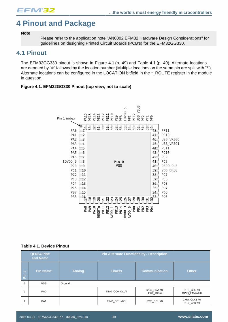
...the world's most energy friendly microcontrollers
2016-03-21 - EFM32GG330FXX - d0038_Rev1.40 49 www.silabs.com
4 Pinout and PackageNote
Please refer to the application note "AN0002 EFM32 Hardware Design Considerations" forguidelines on designing Printed Circuit Boards (PCB's) for the EFM32GG330.
4.1 PinoutThe EFM32GG330 pinout is shown in Figure 4.1 (p. 49) and Table 4.1 (p. 49) . Alternate locationsare denoted by "#" followed by the location number (Multiple locations on the same pin are split with "/").Alternate locations can be configured in the LOCATION bitfield in the *_ROUTE register in the modulein question.
Figure 4.1. EFM32GG330 Pinout (top view, not to scale)
Table 4.1. Device Pinout
QFN64 Pin#and Name
Pin Alternate Functionality / Description
Pin
# Pin Name Analog Timers Communication Other
0 VSS Ground.
1 PA0 TIM0_CC0 #0/1/4I2C0_SDA #0LEU0_RX #4
PRS_CH0 #0GPIO_EM4WU0
2 PA1 TIM0_CC1 #0/1 I2C0_SCL #0CMU_CLK1 #0PRS_CH1 #0
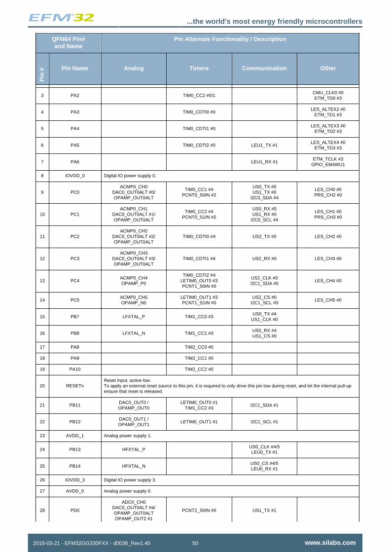
...the world's most energy friendly microcontrollers
2016-03-21 - EFM32GG330FXX - d0038_Rev1.40 50 www.silabs.com
QFN64 Pin#and Name
Pin Alternate Functionality / DescriptionP
in # Pin Name Analog Timers Communication Other
3 PA2 TIM0_CC2 #0/1 CMU_CLK0 #0ETM_TD0 #3
4 PA3 TIM0_CDTI0 #0 LES_ALTEX2 #0
ETM_TD1 #3
5 PA4 TIM0_CDTI1 #0 LES_ALTEX3 #0
ETM_TD2 #3
6 PA5 TIM0_CDTI2 #0 LEU1_TX #1LES_ALTEX4 #0
ETM_TD3 #3
7 PA6 LEU1_RX #1ETM_TCLK #3
GPIO_EM4WU1
8 IOVDD_0 Digital IO power supply 0.
9 PC0ACMP0_CH0
DAC0_OUT0ALT #0/OPAMP_OUT0ALT
TIM0_CC1 #4PCNT0_S0IN #2
US0_TX #5US1_TX #0
I2C0_SDA #4
LES_CH0 #0PRS_CH2 #0
10 PC1ACMP0_CH1
DAC0_OUT0ALT #1/OPAMP_OUT0ALT
TIM0_CC2 #4PCNT0_S1IN #2
US0_RX #5US1_RX #0
I2C0_SCL #4
LES_CH1 #0PRS_CH3 #0
11 PC2ACMP0_CH2
DAC0_OUT0ALT #2/OPAMP_OUT0ALT
TIM0_CDTI0 #4 US2_TX #0 LES_CH2 #0
12 PC3ACMP0_CH3
DAC0_OUT0ALT #3/OPAMP_OUT0ALT
TIM0_CDTI1 #4 US2_RX #0 LES_CH3 #0
13 PC4ACMP0_CH4OPAMP_P0
TIM0_CDTI2 #4LETIM0_OUT0 #3PCNT1_S0IN #0
US2_CLK #0I2C1_SDA #0
LES_CH4 #0
14 PC5ACMP0_CH5OPAMP_N0
LETIM0_OUT1 #3PCNT1_S1IN #0
US2_CS #0I2C1_SCL #0
LES_CH5 #0
15 PB7 LFXTAL_P TIM1_CC0 #3US0_TX #4
US1_CLK #0
16 PB8 LFXTAL_N TIM1_CC1 #3US0_RX #4US1_CS #0
17 PA8 TIM2_CC0 #0
18 PA9 TIM2_CC1 #0
19 PA10 TIM2_CC2 #0
20 RESETnReset input, active low.To apply an external reset source to this pin, it is required to only drive this pin low during reset, and let the internal pull-upensure that reset is released.
21 PB11DAC0_OUT0 /OPAMP_OUT0
LETIM0_OUT0 #1TIM1_CC2 #3
I2C1_SDA #1
22 PB12DAC0_OUT1 /OPAMP_OUT1
LETIM0_OUT1 #1 I2C1_SCL #1
23 AVDD_1 Analog power supply 1.
24 PB13 HFXTAL_P US0_CLK #4/5LEU0_TX #1
25 PB14 HFXTAL_N US0_CS #4/5LEU0_RX #1
26 IOVDD_3 Digital IO power supply 3.
27 AVDD_0 Analog power supply 0.
28 PD0
ADC0_CH0DAC0_OUT0ALT #4/OPAMP_OUT0ALTOPAMP_OUT2 #1
PCNT2_S0IN #0 US1_TX #1
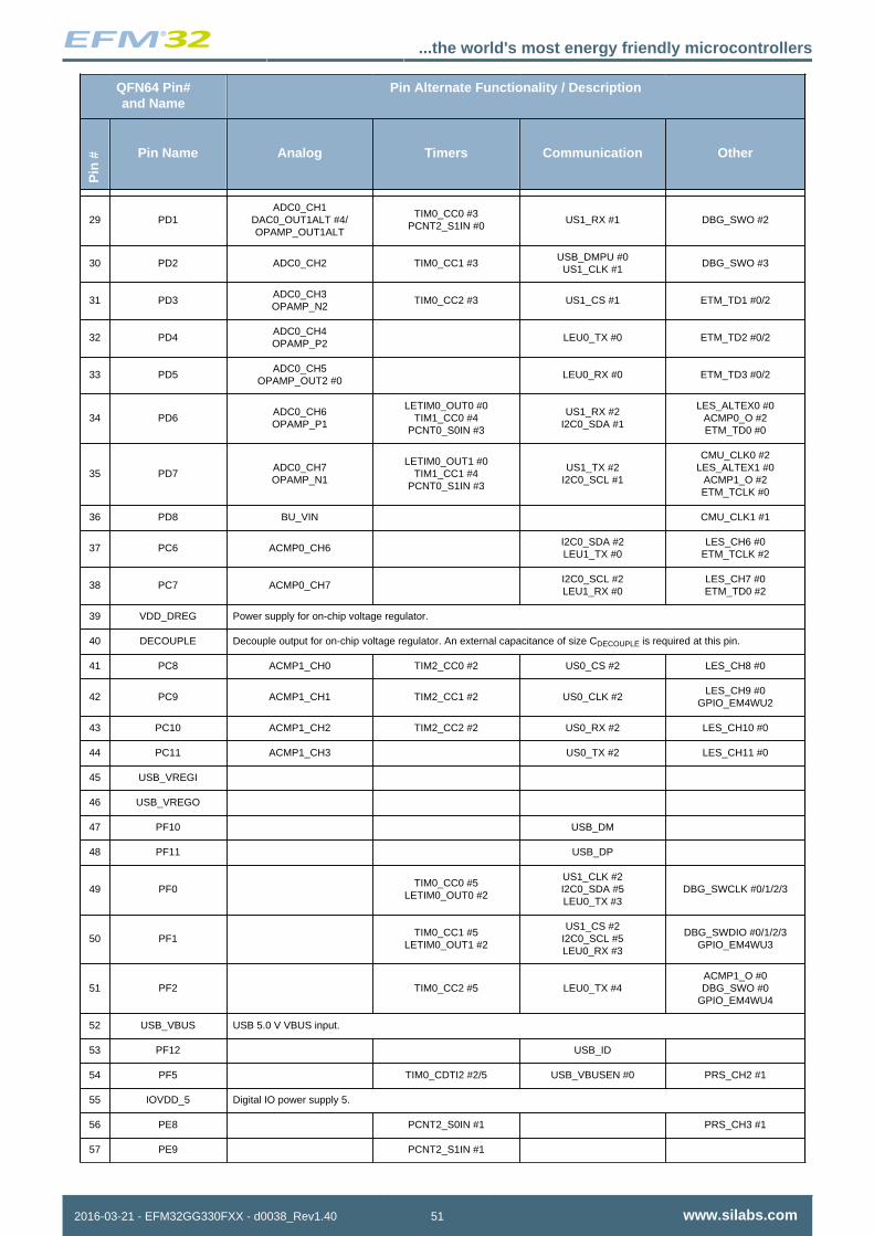
...the world's most energy friendly microcontrollers
2016-03-21 - EFM32GG330FXX - d0038_Rev1.40 51 www.silabs.com
QFN64 Pin#and Name
Pin Alternate Functionality / DescriptionP
in # Pin Name Analog Timers Communication Other
29 PD1ADC0_CH1
DAC0_OUT1ALT #4/OPAMP_OUT1ALT
TIM0_CC0 #3PCNT2_S1IN #0
US1_RX #1 DBG_SWO #2
30 PD2 ADC0_CH2 TIM0_CC1 #3USB_DMPU #0US1_CLK #1
DBG_SWO #3
31 PD3ADC0_CH3OPAMP_N2
TIM0_CC2 #3 US1_CS #1 ETM_TD1 #0/2
32 PD4ADC0_CH4OPAMP_P2
LEU0_TX #0 ETM_TD2 #0/2
33 PD5ADC0_CH5
OPAMP_OUT2 #0 LEU0_RX #0 ETM_TD3 #0/2
34 PD6ADC0_CH6OPAMP_P1
LETIM0_OUT0 #0TIM1_CC0 #4
PCNT0_S0IN #3
US1_RX #2I2C0_SDA #1
LES_ALTEX0 #0ACMP0_O #2ETM_TD0 #0
35 PD7ADC0_CH7OPAMP_N1
LETIM0_OUT1 #0TIM1_CC1 #4
PCNT0_S1IN #3
US1_TX #2I2C0_SCL #1
CMU_CLK0 #2LES_ALTEX1 #0
ACMP1_O #2ETM_TCLK #0
36 PD8 BU_VIN CMU_CLK1 #1
37 PC6 ACMP0_CH6 I2C0_SDA #2LEU1_TX #0
LES_CH6 #0ETM_TCLK #2
38 PC7 ACMP0_CH7 I2C0_SCL #2LEU1_RX #0
LES_CH7 #0ETM_TD0 #2
39 VDD_DREG Power supply for on-chip voltage regulator.
40 DECOUPLE Decouple output for on-chip voltage regulator. An external capacitance of size CDECOUPLE is required at this pin.
41 PC8 ACMP1_CH0 TIM2_CC0 #2 US0_CS #2 LES_CH8 #0
42 PC9 ACMP1_CH1 TIM2_CC1 #2 US0_CLK #2LES_CH9 #0
GPIO_EM4WU2
43 PC10 ACMP1_CH2 TIM2_CC2 #2 US0_RX #2 LES_CH10 #0
44 PC11 ACMP1_CH3 US0_TX #2 LES_CH11 #0
45 USB_VREGI
46 USB_VREGO
47 PF10 USB_DM
48 PF11 USB_DP
49 PF0 TIM0_CC0 #5
LETIM0_OUT0 #2
US1_CLK #2I2C0_SDA #5LEU0_TX #3
DBG_SWCLK #0/1/2/3
50 PF1 TIM0_CC1 #5
LETIM0_OUT1 #2
US1_CS #2I2C0_SCL #5LEU0_RX #3
DBG_SWDIO #0/1/2/3GPIO_EM4WU3
51 PF2 TIM0_CC2 #5 LEU0_TX #4ACMP1_O #0DBG_SWO #0
GPIO_EM4WU4
52 USB_VBUS USB 5.0 V VBUS input.
53 PF12 USB_ID
54 PF5 TIM0_CDTI2 #2/5 USB_VBUSEN #0 PRS_CH2 #1
55 IOVDD_5 Digital IO power supply 5.
56 PE8 PCNT2_S0IN #1 PRS_CH3 #1
57 PE9 PCNT2_S1IN #1
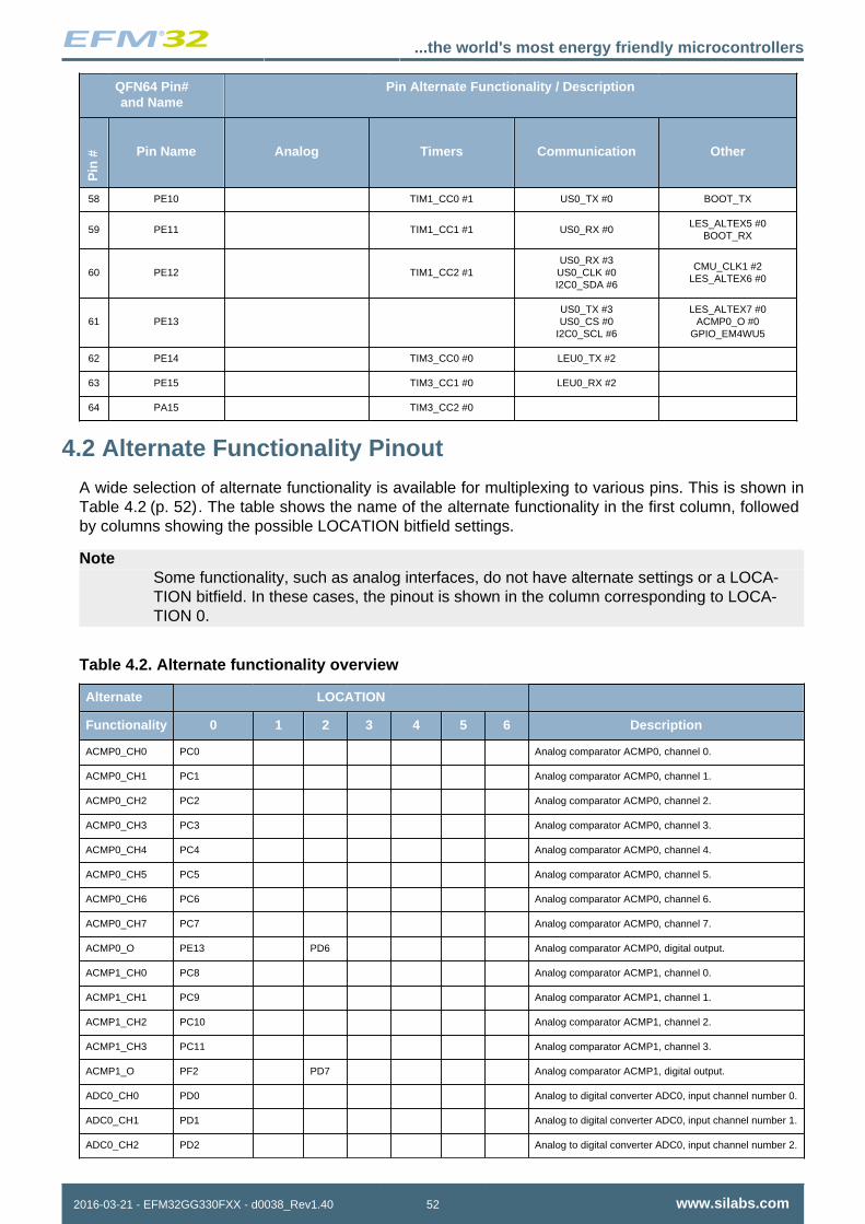
...the world's most energy friendly microcontrollers
2016-03-21 - EFM32GG330FXX - d0038_Rev1.40 52 www.silabs.com
QFN64 Pin#and Name
Pin Alternate Functionality / DescriptionP
in # Pin Name Analog Timers Communication Other
58 PE10 TIM1_CC0 #1 US0_TX #0 BOOT_TX
59 PE11 TIM1_CC1 #1 US0_RX #0LES_ALTEX5 #0
BOOT_RX
60 PE12 TIM1_CC2 #1US0_RX #3
US0_CLK #0I2C0_SDA #6
CMU_CLK1 #2LES_ALTEX6 #0
61 PE13 US0_TX #3US0_CS #0
I2C0_SCL #6
LES_ALTEX7 #0ACMP0_O #0
GPIO_EM4WU5
62 PE14 TIM3_CC0 #0 LEU0_TX #2
63 PE15 TIM3_CC1 #0 LEU0_RX #2
64 PA15 TIM3_CC2 #0
4.2 Alternate Functionality Pinout
A wide selection of alternate functionality is available for multiplexing to various pins. This is shown inTable 4.2 (p. 52) . The table shows the name of the alternate functionality in the first column, followedby columns showing the possible LOCATION bitfield settings.
NoteSome functionality, such as analog interfaces, do not have alternate settings or a LOCA-TION bitfield. In these cases, the pinout is shown in the column corresponding to LOCA-TION 0.
Table 4.2. Alternate functionality overview
Alternate LOCATION
Functionality 0 1 2 3 4 5 6 Description
ACMP0_CH0 PC0 Analog comparator ACMP0, channel 0.
ACMP0_CH1 PC1 Analog comparator ACMP0, channel 1.
ACMP0_CH2 PC2 Analog comparator ACMP0, channel 2.
ACMP0_CH3 PC3 Analog comparator ACMP0, channel 3.
ACMP0_CH4 PC4 Analog comparator ACMP0, channel 4.
ACMP0_CH5 PC5 Analog comparator ACMP0, channel 5.
ACMP0_CH6 PC6 Analog comparator ACMP0, channel 6.
ACMP0_CH7 PC7 Analog comparator ACMP0, channel 7.
ACMP0_O PE13 PD6 Analog comparator ACMP0, digital output.
ACMP1_CH0 PC8 Analog comparator ACMP1, channel 0.
ACMP1_CH1 PC9 Analog comparator ACMP1, channel 1.
ACMP1_CH2 PC10 Analog comparator ACMP1, channel 2.
ACMP1_CH3 PC11 Analog comparator ACMP1, channel 3.
ACMP1_O PF2 PD7 Analog comparator ACMP1, digital output.
ADC0_CH0 PD0 Analog to digital converter ADC0, input channel number 0.
ADC0_CH1 PD1 Analog to digital converter ADC0, input channel number 1.
ADC0_CH2 PD2 Analog to digital converter ADC0, input channel number 2.
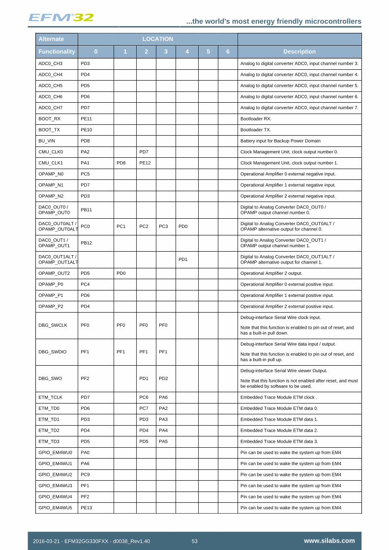
...the world's most energy friendly microcontrollers
2016-03-21 - EFM32GG330FXX - d0038_Rev1.40 53 www.silabs.com
Alternate LOCATION
Functionality 0 1 2 3 4 5 6 Description
ADC0_CH3 PD3 Analog to digital converter ADC0, input channel number 3.
ADC0_CH4 PD4 Analog to digital converter ADC0, input channel number 4.
ADC0_CH5 PD5 Analog to digital converter ADC0, input channel number 5.
ADC0_CH6 PD6 Analog to digital converter ADC0, input channel number 6.
ADC0_CH7 PD7 Analog to digital converter ADC0, input channel number 7.
BOOT_RX PE11 Bootloader RX.
BOOT_TX PE10 Bootloader TX.
BU_VIN PD8 Battery input for Backup Power Domain
CMU_CLK0 PA2 PD7 Clock Management Unit, clock output number 0.
CMU_CLK1 PA1 PD8 PE12 Clock Management Unit, clock output number 1.
OPAMP_N0 PC5 Operational Amplifier 0 external negative input.
OPAMP_N1 PD7 Operational Amplifier 1 external negative input.
OPAMP_N2 PD3 Operational Amplifier 2 external negative input.
DAC0_OUT0 /OPAMP_OUT0
PB11 Digital to Analog Converter DAC0_OUT0 /OPAMP output channel number 0.
DAC0_OUT0ALT /OPAMP_OUT0ALT
PC0 PC1 PC2 PC3 PD0 Digital to Analog Converter DAC0_OUT0ALT /OPAMP alternative output for channel 0.
DAC0_OUT1 /OPAMP_OUT1
PB12 Digital to Analog Converter DAC0_OUT1 /OPAMP output channel number 1.
DAC0_OUT1ALT /OPAMP_OUT1ALT
PD1 Digital to Analog Converter DAC0_OUT1ALT /OPAMP alternative output for channel 1.
OPAMP_OUT2 PD5 PD0 Operational Amplifier 2 output.
OPAMP_P0 PC4 Operational Amplifier 0 external positive input.
OPAMP_P1 PD6 Operational Amplifier 1 external positive input.
OPAMP_P2 PD4 Operational Amplifier 2 external positive input.
DBG_SWCLK PF0 PF0 PF0 PF0
Debug-interface Serial Wire clock input.
Note that this function is enabled to pin out of reset, andhas a built-in pull down.
DBG_SWDIO PF1 PF1 PF1 PF1
Debug-interface Serial Wire data input / output.
Note that this function is enabled to pin out of reset, andhas a built-in pull up.
DBG_SWO PF2 PD1 PD2
Debug-interface Serial Wire viewer Output.
Note that this function is not enabled after reset, and mustbe enabled by software to be used.
ETM_TCLK PD7 PC6 PA6 Embedded Trace Module ETM clock .
ETM_TD0 PD6 PC7 PA2 Embedded Trace Module ETM data 0.
ETM_TD1 PD3 PD3 PA3 Embedded Trace Module ETM data 1.
ETM_TD2 PD4 PD4 PA4 Embedded Trace Module ETM data 2.
ETM_TD3 PD5 PD5 PA5 Embedded Trace Module ETM data 3.
GPIO_EM4WU0 PA0 Pin can be used to wake the system up from EM4
GPIO_EM4WU1 PA6 Pin can be used to wake the system up from EM4
GPIO_EM4WU2 PC9 Pin can be used to wake the system up from EM4
GPIO_EM4WU3 PF1 Pin can be used to wake the system up from EM4
GPIO_EM4WU4 PF2 Pin can be used to wake the system up from EM4
GPIO_EM4WU5 PE13 Pin can be used to wake the system up from EM4
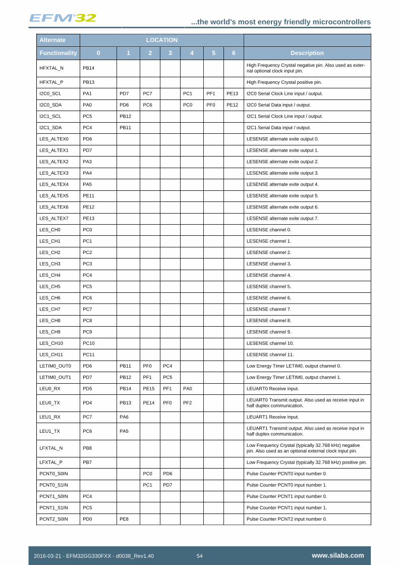
...the world's most energy friendly microcontrollers
2016-03-21 - EFM32GG330FXX - d0038_Rev1.40 54 www.silabs.com
Alternate LOCATION
Functionality 0 1 2 3 4 5 6 Description
HFXTAL_N PB14 High Frequency Crystal negative pin. Also used as exter-nal optional clock input pin.
HFXTAL_P PB13 High Frequency Crystal positive pin.
I2C0_SCL PA1 PD7 PC7 PC1 PF1 PE13 I2C0 Serial Clock Line input / output.
I2C0_SDA PA0 PD6 PC6 PC0 PF0 PE12 I2C0 Serial Data input / output.
I2C1_SCL PC5 PB12 I2C1 Serial Clock Line input / output.
I2C1_SDA PC4 PB11 I2C1 Serial Data input / output.
LES_ALTEX0 PD6 LESENSE alternate exite output 0.
LES_ALTEX1 PD7 LESENSE alternate exite output 1.
LES_ALTEX2 PA3 LESENSE alternate exite output 2.
LES_ALTEX3 PA4 LESENSE alternate exite output 3.
LES_ALTEX4 PA5 LESENSE alternate exite output 4.
LES_ALTEX5 PE11 LESENSE alternate exite output 5.
LES_ALTEX6 PE12 LESENSE alternate exite output 6.
LES_ALTEX7 PE13 LESENSE alternate exite output 7.
LES_CH0 PC0 LESENSE channel 0.
LES_CH1 PC1 LESENSE channel 1.
LES_CH2 PC2 LESENSE channel 2.
LES_CH3 PC3 LESENSE channel 3.
LES_CH4 PC4 LESENSE channel 4.
LES_CH5 PC5 LESENSE channel 5.
LES_CH6 PC6 LESENSE channel 6.
LES_CH7 PC7 LESENSE channel 7.
LES_CH8 PC8 LESENSE channel 8.
LES_CH9 PC9 LESENSE channel 9.
LES_CH10 PC10 LESENSE channel 10.
LES_CH11 PC11 LESENSE channel 11.
LETIM0_OUT0 PD6 PB11 PF0 PC4 Low Energy Timer LETIM0, output channel 0.
LETIM0_OUT1 PD7 PB12 PF1 PC5 Low Energy Timer LETIM0, output channel 1.
LEU0_RX PD5 PB14 PE15 PF1 PA0 LEUART0 Receive input.
LEU0_TX PD4 PB13 PE14 PF0 PF2 LEUART0 Transmit output. Also used as receive input inhalf duplex communication.
LEU1_RX PC7 PA6 LEUART1 Receive input.
LEU1_TX PC6 PA5 LEUART1 Transmit output. Also used as receive input inhalf duplex communication.
LFXTAL_N PB8 Low Frequency Crystal (typically 32.768 kHz) negativepin. Also used as an optional external clock input pin.
LFXTAL_P PB7 Low Frequency Crystal (typically 32.768 kHz) positive pin.
PCNT0_S0IN PC0 PD6 Pulse Counter PCNT0 input number 0.
PCNT0_S1IN PC1 PD7 Pulse Counter PCNT0 input number 1.
PCNT1_S0IN PC4 Pulse Counter PCNT1 input number 0.
PCNT1_S1IN PC5 Pulse Counter PCNT1 input number 1.
PCNT2_S0IN PD0 PE8 Pulse Counter PCNT2 input number 0.
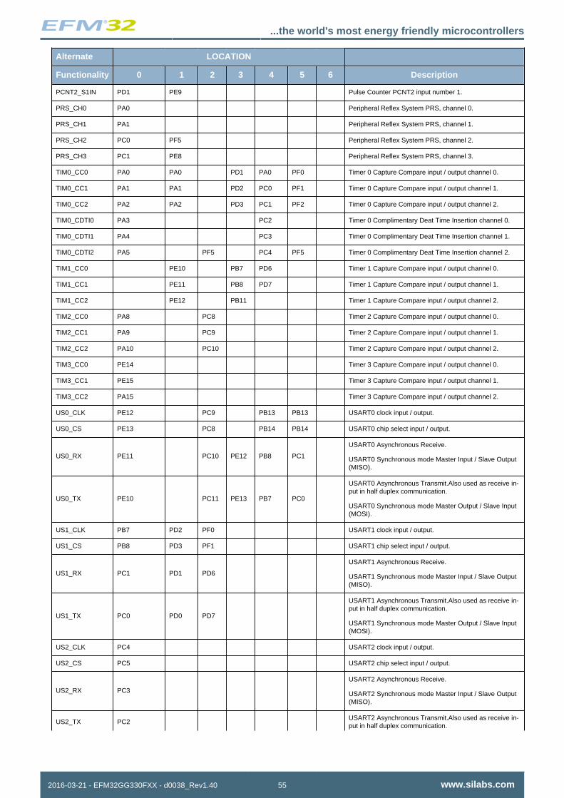
...the world's most energy friendly microcontrollers
2016-03-21 - EFM32GG330FXX - d0038_Rev1.40 55 www.silabs.com
Alternate LOCATION
Functionality 0 1 2 3 4 5 6 Description
PCNT2_S1IN PD1 PE9 Pulse Counter PCNT2 input number 1.
PRS_CH0 PA0 Peripheral Reflex System PRS, channel 0.
PRS_CH1 PA1 Peripheral Reflex System PRS, channel 1.
PRS_CH2 PC0 PF5 Peripheral Reflex System PRS, channel 2.
PRS_CH3 PC1 PE8 Peripheral Reflex System PRS, channel 3.
TIM0_CC0 PA0 PA0 PD1 PA0 PF0 Timer 0 Capture Compare input / output channel 0.
TIM0_CC1 PA1 PA1 PD2 PC0 PF1 Timer 0 Capture Compare input / output channel 1.
TIM0_CC2 PA2 PA2 PD3 PC1 PF2 Timer 0 Capture Compare input / output channel 2.
TIM0_CDTI0 PA3 PC2 Timer 0 Complimentary Deat Time Insertion channel 0.
TIM0_CDTI1 PA4 PC3 Timer 0 Complimentary Deat Time Insertion channel 1.
TIM0_CDTI2 PA5 PF5 PC4 PF5 Timer 0 Complimentary Deat Time Insertion channel 2.
TIM1_CC0 PE10 PB7 PD6 Timer 1 Capture Compare input / output channel 0.
TIM1_CC1 PE11 PB8 PD7 Timer 1 Capture Compare input / output channel 1.
TIM1_CC2 PE12 PB11 Timer 1 Capture Compare input / output channel 2.
TIM2_CC0 PA8 PC8 Timer 2 Capture Compare input / output channel 0.
TIM2_CC1 PA9 PC9 Timer 2 Capture Compare input / output channel 1.
TIM2_CC2 PA10 PC10 Timer 2 Capture Compare input / output channel 2.
TIM3_CC0 PE14 Timer 3 Capture Compare input / output channel 0.
TIM3_CC1 PE15 Timer 3 Capture Compare input / output channel 1.
TIM3_CC2 PA15 Timer 3 Capture Compare input / output channel 2.
US0_CLK PE12 PC9 PB13 PB13 USART0 clock input / output.
US0_CS PE13 PC8 PB14 PB14 USART0 chip select input / output.
US0_RX PE11 PC10 PE12 PB8 PC1
USART0 Asynchronous Receive.
USART0 Synchronous mode Master Input / Slave Output(MISO).
US0_TX PE10 PC11 PE13 PB7 PC0
USART0 Asynchronous Transmit.Also used as receive in-put in half duplex communication.
USART0 Synchronous mode Master Output / Slave Input(MOSI).
US1_CLK PB7 PD2 PF0 USART1 clock input / output.
US1_CS PB8 PD3 PF1 USART1 chip select input / output.
US1_RX PC1 PD1 PD6
USART1 Asynchronous Receive.
USART1 Synchronous mode Master Input / Slave Output(MISO).
US1_TX PC0 PD0 PD7
USART1 Asynchronous Transmit.Also used as receive in-put in half duplex communication.
USART1 Synchronous mode Master Output / Slave Input(MOSI).
US2_CLK PC4 USART2 clock input / output.
US2_CS PC5 USART2 chip select input / output.
US2_RX PC3
USART2 Asynchronous Receive.
USART2 Synchronous mode Master Input / Slave Output(MISO).
US2_TX PC2 USART2 Asynchronous Transmit.Also used as receive in-put in half duplex communication.
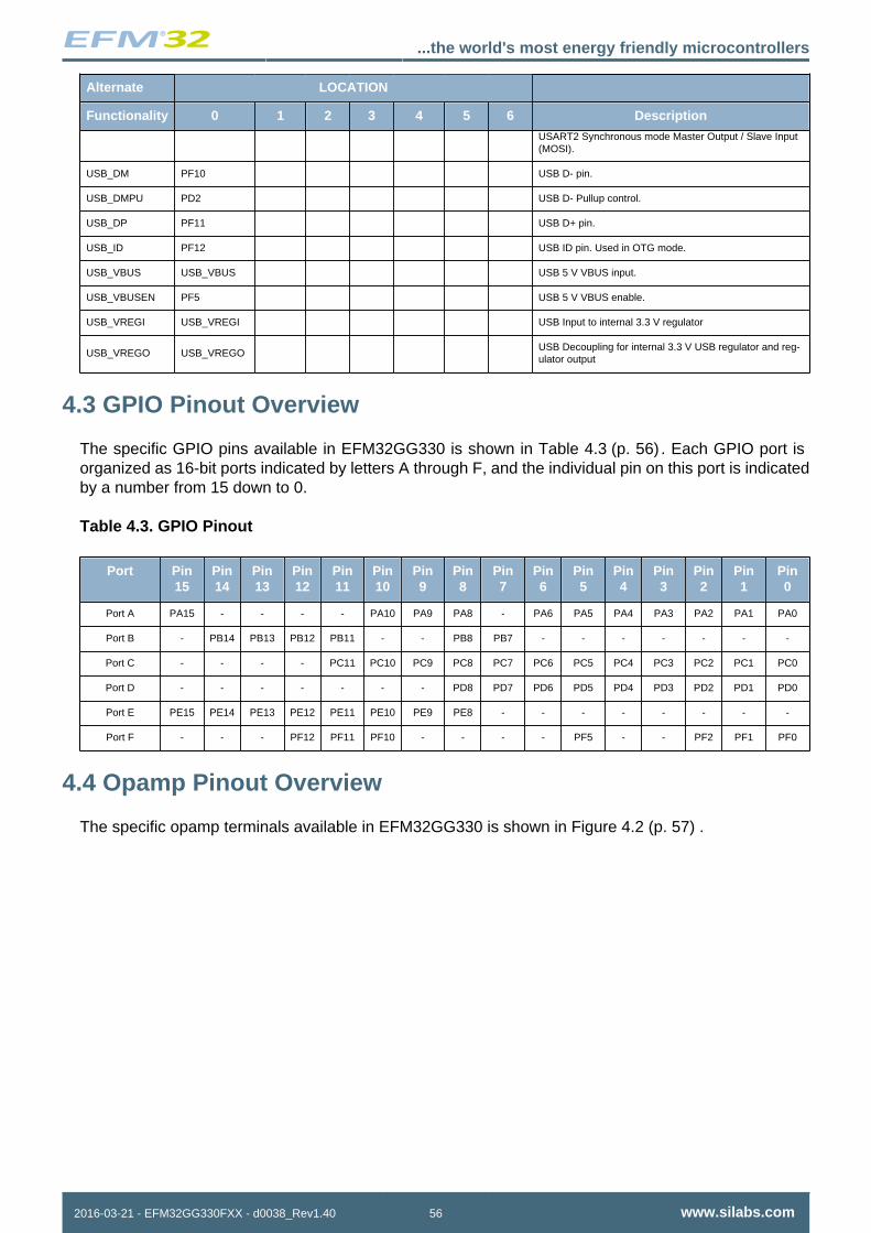
...the world's most energy friendly microcontrollers
2016-03-21 - EFM32GG330FXX - d0038_Rev1.40 56 www.silabs.com
Alternate LOCATION
Functionality 0 1 2 3 4 5 6 Description
USART2 Synchronous mode Master Output / Slave Input(MOSI).
USB_DM PF10 USB D- pin.
USB_DMPU PD2 USB D- Pullup control.
USB_DP PF11 USB D+ pin.
USB_ID PF12 USB ID pin. Used in OTG mode.
USB_VBUS USB_VBUS USB 5 V VBUS input.
USB_VBUSEN PF5 USB 5 V VBUS enable.
USB_VREGI USB_VREGI USB Input to internal 3.3 V regulator
USB_VREGO USB_VREGO USB Decoupling for internal 3.3 V USB regulator and reg-ulator output
4.3 GPIO Pinout Overview
The specific GPIO pins available in EFM32GG330 is shown in Table 4.3 (p. 56) . Each GPIO port isorganized as 16-bit ports indicated by letters A through F, and the individual pin on this port is indicatedby a number from 15 down to 0.
Table 4.3. GPIO Pinout
Port Pin15
Pin14
Pin13
Pin12
Pin11
Pin10
Pin9
Pin8
Pin7
Pin6
Pin5
Pin4
Pin3
Pin2
Pin1
Pin0
Port A PA15 - - - - PA10 PA9 PA8 - PA6 PA5 PA4 PA3 PA2 PA1 PA0
Port B - PB14 PB13 PB12 PB11 - - PB8 PB7 - - - - - - -
Port C - - - - PC11 PC10 PC9 PC8 PC7 PC6 PC5 PC4 PC3 PC2 PC1 PC0
Port D - - - - - - - PD8 PD7 PD6 PD5 PD4 PD3 PD2 PD1 PD0
Port E PE15 PE14 PE13 PE12 PE11 PE10 PE9 PE8 - - - - - - - -
Port F - - - PF12 PF11 PF10 - - - - PF5 - - PF2 PF1 PF0
4.4 Opamp Pinout Overview
The specific opamp terminals available in EFM32GG330 is shown in Figure 4.2 (p. 57) .
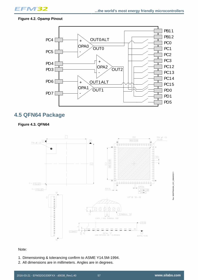
...the world's most energy friendly microcontrollers
2016-03-21 - EFM32GG330FXX - d0038_Rev1.40 57 www.silabs.com
Figure 4.2. Opamp Pinout
-
+OPA0
-
+OPA2
-
+OPA1
OUT0ALT
OUT0
OUT2
OUT1ALT
OUT1
PC4
PC5
PD4PD3
PD6
PD7
PB11PB12PC0PC1PC2PC3PC12PC13PC14PC15PD0PD1PD5
4.5 QFN64 Package
Figure 4.3. QFN64
Note:
1. Dimensioning & tolerancing confirm to ASME Y14.5M-1994.2. All dimensions are in millimeters. Angles are in degrees.
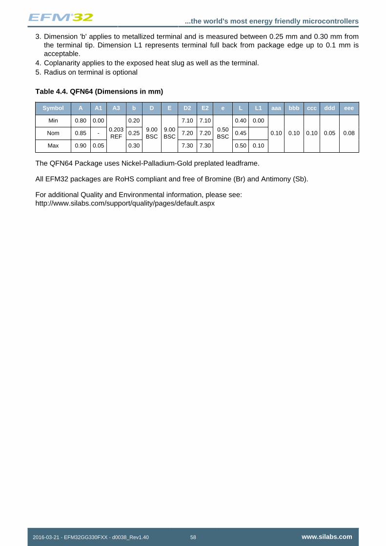
...the world's most energy friendly microcontrollers
2016-03-21 - EFM32GG330FXX - d0038_Rev1.40 58 www.silabs.com
3. Dimension 'b' applies to metallized terminal and is measured between 0.25 mm and 0.30 mm fromthe terminal tip. Dimension L1 represents terminal full back from package edge up to 0.1 mm isacceptable.
4. Coplanarity applies to the exposed heat slug as well as the terminal.5. Radius on terminal is optional
Table 4.4. QFN64 (Dimensions in mm)
Symbol A A1 A3 b D E D2 E2 e L L1 aaa bbb ccc ddd eee
Min 0.80 0.00 0.20 7.10 7.10 0.40 0.00
Nom 0.85 - 0.25 7.20 7.20 0.45
Max 0.90 0.05
0.203REF
0.30
9.00BSC
9.00BSC
7.30 7.30
0.50BSC
0.50 0.10
0.10 0.10 0.10 0.05 0.08
The QFN64 Package uses Nickel-Palladium-Gold preplated leadframe.
All EFM32 packages are RoHS compliant and free of Bromine (Br) and Antimony (Sb).
For additional Quality and Environmental information, please see:http://www.silabs.com/support/quality/pages/default.aspx
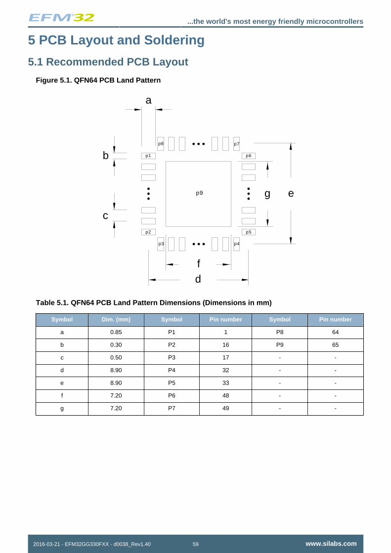
...the world's most energy friendly microcontrollers
2016-03-21 - EFM32GG330FXX - d0038_Rev1.40 59 www.silabs.com
5 PCB Layout and Soldering
5.1 Recommended PCB Layout
Figure 5.1. QFN64 PCB Land Pattern
e
a
d
p1
p2
p3 p4
p5
p6
p7p8
c
b
p9
f
g
Table 5.1. QFN64 PCB Land Pattern Dimensions (Dimensions in mm)
Symbol Dim. (mm) Symbol Pin number Symbol Pin number
a 0.85 P1 1 P8 64
b 0.30 P2 16 P9 65
c 0.50 P3 17 - -
d 8.90 P4 32 - -
e 8.90 P5 33 - -
f 7.20 P6 48 - -
g 7.20 P7 49 - -
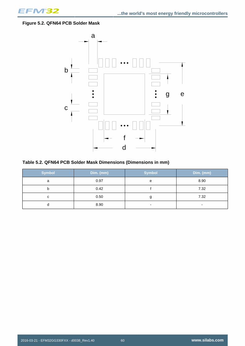
...the world's most energy friendly microcontrollers
2016-03-21 - EFM32GG330FXX - d0038_Rev1.40 60 www.silabs.com
Figure 5.2. QFN64 PCB Solder Mask
e
a
d
c
b
f
g
Table 5.2. QFN64 PCB Solder Mask Dimensions (Dimensions in mm)
Symbol Dim. (mm) Symbol Dim. (mm)
a 0.97 e 8.90
b 0.42 f 7.32
c 0.50 g 7.32
d 8.90 - -
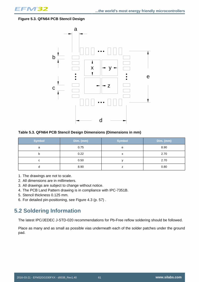
...the world's most energy friendly microcontrollers
2016-03-21 - EFM32GG330FXX - d0038_Rev1.40 61 www.silabs.com
Figure 5.3. QFN64 PCB Stencil Design
e
a
d
c
b
x y
z
Table 5.3. QFN64 PCB Stencil Design Dimensions (Dimensions in mm)
Symbol Dim. (mm) Symbol Dim. (mm)
a 0.75 e 8.90
b 0.22 x 2.70
c 0.50 y 2.70
d 8.90 z 0.80
1. The drawings are not to scale.2. All dimensions are in millimeters.3. All drawings are subject to change without notice.4. The PCB Land Pattern drawing is in compliance with IPC-7351B.5. Stencil thickness 0.125 mm.6. For detailed pin-positioning, see Figure 4.3 (p. 57) .
5.2 Soldering Information
The latest IPC/JEDEC J-STD-020 recommendations for Pb-Free reflow soldering should be followed.
Place as many and as small as possible vias underneath each of the solder patches under the groundpad.
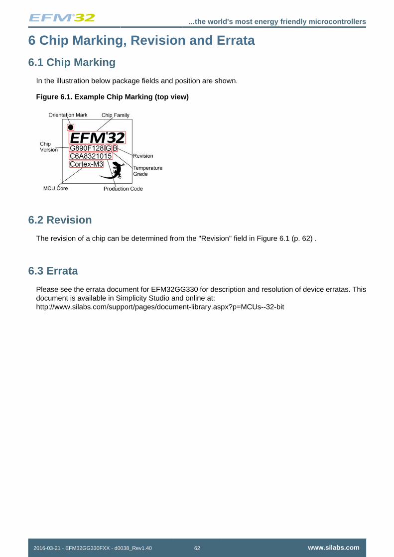
...the world's most energy friendly microcontrollers
2016-03-21 - EFM32GG330FXX - d0038_Rev1.40 62 www.silabs.com
6 Chip Marking, Revision and Errata
6.1 Chip Marking
In the illustration below package fields and position are shown.
Figure 6.1. Example Chip Marking (top view)
6.2 Revision
The revision of a chip can be determined from the "Revision" field in Figure 6.1 (p. 62) .
6.3 Errata
Please see the errata document for EFM32GG330 for description and resolution of device erratas. Thisdocument is available in Simplicity Studio and online at:http://www.silabs.com/support/pages/document-library.aspx?p=MCUs--32-bit
...the world's most energy friendly microcontrollers
2016-03-21 - EFM32GG330FXX - d0038_Rev1.40 63 www.silabs.com
7 Revision History
7.1 Revision 1.40
March 21st, 2016
Added clarification on conditions for INLADC and DNLADC parameters.
Reduced maximum and typical current consumption for all EM0 entries except 48 MHz in the CurrentConsumption table in the Electrical Characteristics section.
Increased maximum specifications for EM2 current, EM3 current, and EM4 current in the Current Con-sumption table in the Electrical Characteristics section.
Increased typical specification for EM2 and EM3 current at 85 C in the Current Consumption table inthe Electrical Characteristics section.
Added EM2, EM3, and EM4 current consumption vs. temperature graphs.
Added a new EM2 entry and specified the existing specification is for EM0 for the BOD threshold onfalling external supply voltage in the Power Management table in the Electrical Characteristics section.
Reduced maximum input leakage current in the GPIO table in the Electrical Characteristics section.
Added a maximum current consumption specification to the LFRCO table in the Electrical Characteristicssection.
Added maximum specifications for the active current including references for two channels to the DACtable in the Electrical Characteristics section.
Increased the maximum specification for DAC offset voltage in the DAC table in the Electrical Charac-teristics section.
Increased the typical specifications for active current with FULLBIAS=1 and capacitive sense internalresistance in the ACMP table in the Electrical Characteristics section.
Added minimum and maximum specifications and updated the typical value for the VCMP offset voltagein the VCMP table in the Electrical Characteristics section.
Removed the maximum specification and reduced the typical value for hysteresis in the VCMP table inthe Electrical Characteristics section.
Updated all graphs in the Electrical Characteristics section to display data for 2.0 V as the minimumvoltage.
7.2 Revision 1.30
May 23rd, 2014
Removed "preliminary" markings
Updated HFRCO figures.
Corrected single power supply voltage minimum value from 1.85V to 1.98V.
Updated Current Consumption information.
Updated Power Management information.
...the world's most energy friendly microcontrollers
2016-03-21 - EFM32GG330FXX - d0038_Rev1.40 64 www.silabs.com
Updated GPIO information.
Updated LFRCO information.
Updated HFRCO information.
Updated ULFRCO information.
Updated ADC information.
Updated DAC information.
Updated OPAMP information.
Updated ACMP information.
Updated VCMP information.
Added AUXHFRCO information.
7.3 Revision 1.21
November 21st, 2013
Updated figures.
Updated errata-link.
Updated chip marking.
Added link to Environmental and Quality information.
Re-added missing DAC-data.
7.4 Revision 1.20
September 30th, 2013
Added I2C characterization data.
Added SPI characterization data.
Corrected the DAC and OPAMP2 pin sharing information in the Alternate Functionality Pinout section.
Corrected GPIO operating voltage from 1.8 V to 1.85 V.
Added the USB bootloader information.
Updated that the EM2 current consumption test was carried out with only one RAM block enabled.
Corrected the ADC resolution from 12, 10 and 6 bit to 12, 8 and 6 bit.
Removed UART mentioned incorrectly in the QFN64 parts.
Updated Environmental information.
Updated trademark, disclaimer and contact information.
Other minor corrections.
...the world's most energy friendly microcontrollers
2016-03-21 - EFM32GG330FXX - d0038_Rev1.40 65 www.silabs.com
7.5 Revision 1.10
June 28th, 2013
Updated power requirements in the Power Management section.
Removed minimum load capacitance figure and table. Added reference to application note.
Other minor corrections.
7.6 Revision 1.00
September 11th, 2012
Updated the HFRCO 1 MHz band typical value to 1.2 MHz.
Updated the HFRCO 7 MHz band typical value to 6.6 MHz.
Other minor corrections.
7.7 Revision 0.98
May 25th, 2012
Corrected EM3 current consumption in the Electrical Characteristics section.
7.8 Revision 0.96
February 28th, 2012
Added reference to errata document.
Corrected QFN64 package drawing.
Updated PCB land pattern, solder mask and stencil design.
7.9 Revision 0.95
September 28th, 2011
Flash configuration for Giant Gecko is now 1024KB or 512KB. For flash sizes below 512KB, see theLeopard Gecko Family.
Corrected operating voltage from 1.8 V to 1.85 V.
Added rising POR level to Electrical Characteristics section.
Updated Minimum Load Capacitance (CLFXOL) Requirement For Safe Crystal Startup.
Added Gain error drift and Offset error drift to ADC table.
Added Opamp pinout overview.
Added reference to errata document.
Corrected QFN64 package drawing.
Updated PCB land pattern, solder mask and stencil design.
...the world's most energy friendly microcontrollers
2016-03-21 - EFM32GG330FXX - d0038_Rev1.40 66 www.silabs.com
7.10 Revision 0.91
March 21th, 2011
Added new alternative locations for SWO.
Added new USB Pin to pinout table.
Corrected slew rate data for Opamps.
7.11 Revision 0.90
February 4th, 2011
Initial preliminary release.
...the world's most energy friendly microcontrollers
2016-03-21 - EFM32GG330FXX - d0038_Rev1.40 67 www.silabs.com
A Disclaimer and Trademarks
A.1 Disclaimer
Silicon Laboratories intends to provide customers with the latest, accurate, and in-depth documentationof all peripherals and modules available for system and software implementers using or intending to usethe Silicon Laboratories products. Characterization data, available modules and peripherals, memorysizes and memory addresses refer to each specific device, and "Typical" parameters provided can anddo vary in different applications. Application examples described herein are for illustrative purposes only.Silicon Laboratories reserves the right to make changes without further notice and limitation to productinformation, specifications, and descriptions herein, and does not give warranties as to the accuracyor completeness of the included information. Silicon Laboratories shall have no liability for the conse-quences of use of the information supplied herein. This document does not imply or express copyrightlicenses granted hereunder to design or fabricate any integrated circuits. The products must not beused within any Life Support System without the specific written consent of Silicon Laboratories. A "LifeSupport System" is any product or system intended to support or sustain life and/or health, which, if itfails, can be reasonably expected to result in significant personal injury or death. Silicon Laboratoriesproducts are generally not intended for military applications. Silicon Laboratories products shall under nocircumstances be used in weapons of mass destruction including (but not limited to) nuclear, biologicalor chemical weapons, or missiles capable of delivering such weapons.
A.2 Trademark Information
Silicon Laboratories Inc., Silicon Laboratories, Silicon Labs, SiLabs and the Silicon Labs logo, CMEMS®,EFM, EFM32, EFR, Energy Micro, Energy Micro logo and combinations thereof, "the world’s most ener-gy friendly microcontrollers", Ember®, EZLink®, EZMac®, EZRadio®, EZRadioPRO®, DSPLL®, ISO-modem®, Precision32®, ProSLIC®, SiPHY®, USBXpress® and others are trademarks or registeredtrademarks of Silicon Laboratories Inc. ARM, CORTEX, Cortex-M3 and THUMB are trademarks or reg-istered trademarks of ARM Holdings. Keil is a registered trademark of ARM Limited. All other productsor brand names mentioned herein are trademarks of their respective holders.
...the world's most energy friendly microcontrollers
2016-03-21 - EFM32GG330FXX - d0038_Rev1.40 68 www.silabs.com
B Contact InformationSilicon Laboratories Inc.400 West Cesar ChavezAustin, TX 78701
Please visit the Silicon Labs Technical Support web page:http://www.silabs.com/support/pages/contacttechnicalsupport.aspxand register to submit a technical support request.
...the world's most energy friendly microcontrollers
2016-03-21 - EFM32GG330FXX - d0038_Rev1.40 69 www.silabs.com
Table of Contents1. Ordering Information .................................................................................................................................. 22. System Summary ...................................................................................................................................... 3
2.1. System Introduction ......................................................................................................................... 32.2. Configuration Summary .................................................................................................................... 72.3. Memory Map ................................................................................................................................. 8
3. Electrical Characteristics ........................................................................................................................... 103.1. Test Conditions ............................................................................................................................. 103.2. Absolute Maximum Ratings ............................................................................................................. 103.3. General Operating Conditions .......................................................................................................... 103.4. Current Consumption ..................................................................................................................... 113.5. Transition between Energy Modes .................................................................................................... 133.6. Power Management ....................................................................................................................... 133.7. Flash .......................................................................................................................................... 153.8. General Purpose Input Output ......................................................................................................... 153.9. Oscillators .................................................................................................................................... 233.10. Analog Digital Converter (ADC) ...................................................................................................... 283.11. Digital Analog Converter (DAC) ...................................................................................................... 383.12. Operational Amplifier (OPAMP) ...................................................................................................... 393.13. Analog Comparator (ACMP) .......................................................................................................... 433.14. Voltage Comparator (VCMP) ......................................................................................................... 453.15. I2C ........................................................................................................................................... 453.16. USART SPI ................................................................................................................................ 463.17. USB .......................................................................................................................................... 473.18. Digital Peripherals ....................................................................................................................... 48
4. Pinout and Package ................................................................................................................................. 494.1. Pinout ......................................................................................................................................... 494.2. Alternate Functionality Pinout .......................................................................................................... 524.3. GPIO Pinout Overview ................................................................................................................... 564.4. Opamp Pinout Overview ................................................................................................................. 564.5. QFN64 Package ........................................................................................................................... 57
5. PCB Layout and Soldering ........................................................................................................................ 595.1. Recommended PCB Layout ............................................................................................................ 595.2. Soldering Information ..................................................................................................................... 61
6. Chip Marking, Revision and Errata .............................................................................................................. 626.1. Chip Marking ................................................................................................................................ 626.2. Revision ...................................................................................................................................... 626.3. Errata ......................................................................................................................................... 62
7. Revision History ...................................................................................................................................... 637.1. Revision 1.40 ............................................................................................................................... 637.2. Revision 1.30 ............................................................................................................................... 637.3. Revision 1.21 ............................................................................................................................... 647.4. Revision 1.20 ............................................................................................................................... 647.5. Revision 1.10 ............................................................................................................................... 657.6. Revision 1.00 ............................................................................................................................... 657.7. Revision 0.98 ............................................................................................................................... 657.8. Revision 0.96 ............................................................................................................................... 657.9. Revision 0.95 ............................................................................................................................... 657.10. Revision 0.91 .............................................................................................................................. 667.11. Revision 0.90 .............................................................................................................................. 66
A. Disclaimer and Trademarks ....................................................................................................................... 67A.1. Disclaimer ................................................................................................................................... 67A.2. Trademark Information ................................................................................................................... 67
B. Contact Information ................................................................................................................................. 68B.1. ................................................................................................................................................. 68
...the world's most energy friendly microcontrollers
2016-03-21 - EFM32GG330FXX - d0038_Rev1.40 70 www.silabs.com
List of Figures2.1. Block Diagram ....................................................................................................................................... 32.2. EFM32GG330 Memory Map with largest RAM and Flash sizes ........................................................................ 93.1. EM2 current consumption. RTC prescaled to 1 Hz, 32.768 kHz LFRCO. ......................................................... 123.2. EM3 current consumption. ..................................................................................................................... 123.3. EM4 current consumption. ..................................................................................................................... 133.4. Typical Low-Level Output Current, 2V Supply Voltage .................................................................................. 173.5. Typical High-Level Output Current, 2V Supply Voltage ................................................................................. 183.6. Typical Low-Level Output Current, 3V Supply Voltage .................................................................................. 193.7. Typical High-Level Output Current, 3V Supply Voltage ................................................................................. 203.8. Typical Low-Level Output Current, 3.8V Supply Voltage ............................................................................... 213.9. Typical High-Level Output Current, 3.8V Supply Voltage ............................................................................... 223.10. Calibrated LFRCO Frequency vs Temperature and Supply Voltage .............................................................. 243.11. Calibrated HFRCO 1 MHz Band Frequency vs Supply Voltage and Temperature ............................................ 253.12. Calibrated HFRCO 7 MHz Band Frequency vs Supply Voltage and Temperature ............................................ 253.13. Calibrated HFRCO 11 MHz Band Frequency vs Supply Voltage and Temperature ........................................... 263.14. Calibrated HFRCO 14 MHz Band Frequency vs Supply Voltage and Temperature ........................................... 263.15. Calibrated HFRCO 21 MHz Band Frequency vs Supply Voltage and Temperature ........................................... 263.16. Calibrated HFRCO 28 MHz Band Frequency vs Supply Voltage and Temperature ........................................... 273.17. Integral Non-Linearity (INL) ................................................................................................................... 323.18. Differential Non-Linearity (DNL) .............................................................................................................. 333.19. ADC Frequency Spectrum, Vdd = 3V, Temp = 25°C ................................................................................. 343.20. ADC Integral Linearity Error vs Code, Vdd = 3V, Temp = 25°C ................................................................... 353.21. ADC Differential Linearity Error vs Code, Vdd = 3V, Temp = 25°C ............................................................... 363.22. ADC Absolute Offset, Common Mode = Vdd /2 ........................................................................................ 373.23. ADC Dynamic Performance vs Temperature for all ADC References, Vdd = 3V .............................................. 373.24. ADC Temperature sensor readout ......................................................................................................... 383.25. OPAMP Common Mode Rejection Ratio ................................................................................................. 413.26. OPAMP Positive Power Supply Rejection Ratio ........................................................................................ 413.27. OPAMP Negative Power Supply Rejection Ratio ...................................................................................... 423.28. OPAMP Voltage Noise Spectral Density (Unity Gain) Vout=1V ..................................................................... 423.29. OPAMP Voltage Noise Spectral Density (Non-Unity Gain) .......................................................................... 423.30. ACMP Characteristics, Vdd = 3V, Temp = 25°C, FULLBIAS = 0, HALFBIAS = 1 ............................................. 443.31. SPI Master Timing ............................................................................................................................... 463.32. SPI Slave Timing ................................................................................................................................ 474.1. EFM32GG330 Pinout (top view, not to scale) ............................................................................................. 494.2. Opamp Pinout ...................................................................................................................................... 574.3. QFN64 ................................................................................................................................................ 575.1. QFN64 PCB Land Pattern ...................................................................................................................... 595.2. QFN64 PCB Solder Mask ....................................................................................................................... 605.3. QFN64 PCB Stencil Design .................................................................................................................... 616.1. Example Chip Marking (top view) ............................................................................................................. 62
...the world's most energy friendly microcontrollers
2016-03-21 - EFM32GG330FXX - d0038_Rev1.40 71 www.silabs.com
List of Tables1.1. Ordering Information ................................................................................................................................ 22.1. Configuration Summary ............................................................................................................................ 73.1. Absolute Maximum Ratings ..................................................................................................................... 103.2. General Operating Conditions .................................................................................................................. 103.3. Current Consumption ............................................................................................................................. 113.4. Energy Modes Transitions ...................................................................................................................... 133.5. Power Management ............................................................................................................................... 143.6. Flash .................................................................................................................................................. 153.7. GPIO .................................................................................................................................................. 153.8. LFXO .................................................................................................................................................. 233.9. HFXO ................................................................................................................................................. 233.10. LFRCO .............................................................................................................................................. 243.11. HFRCO ............................................................................................................................................. 243.12. AUXHFRCO ....................................................................................................................................... 273.13. ULFRCO ............................................................................................................................................ 283.14. ADC .................................................................................................................................................. 283.15. DAC .................................................................................................................................................. 383.16. OPAMP ............................................................................................................................................. 393.17. ACMP ............................................................................................................................................... 433.18. VCMP ............................................................................................................................................... 453.19. I2C Standard-mode (Sm) ...................................................................................................................... 453.20. I2C Fast-mode (Fm) ............................................................................................................................ 463.21. I2C Fast-mode Plus (Fm+) .................................................................................................................... 463.22. SPI Master Timing ............................................................................................................................... 473.23. SPI Slave Timing ................................................................................................................................ 473.24. Digital Peripherals ............................................................................................................................... 484.1. Device Pinout ....................................................................................................................................... 494.2. Alternate functionality overview ................................................................................................................ 524.3. GPIO Pinout ........................................................................................................................................ 564.4. QFN64 (Dimensions in mm) .................................................................................................................... 585.1. QFN64 PCB Land Pattern Dimensions (Dimensions in mm) .......................................................................... 595.2. QFN64 PCB Solder Mask Dimensions (Dimensions in mm) ........................................................................... 605.3. QFN64 PCB Stencil Design Dimensions (Dimensions in mm) ........................................................................ 61
...the world's most energy friendly microcontrollers
2016-03-21 - EFM32GG330FXX - d0038_Rev1.40 72 www.silabs.com
List of Equations3.1. Total ACMP Active Current ..................................................................................................................... 433.2. VCMP Trigger Level as a Function of Level Setting ..................................................................................... 45
http://www.silabs.com
Silicon Laboratories Inc.400 West Cesar ChavezAustin, TX 78701USA
Simplicity StudioOne-click access to MCU and wireless tools, documentation, software, source code libraries & more. Available for Windows, Mac and Linux!
IoT Portfoliowww.silabs.com/IoT
SW/HWwww.silabs.com/simplicity
Qualitywww.silabs.com/quality
Support and Communitycommunity.silabs.com
DisclaimerSilicon Laboratories intends to provide customers with the latest, accurate, and in-depth documentation of all peripherals and modules available for system and software implementers using or intending to use the Silicon Laboratories products. Characterization data, available modules and peripherals, memory sizes and memory addresses refer to each specific device, and "Typical" parameters provided can and do vary in different applications. Application examples described herein are for illustrative purposes only. Silicon Laboratories reserves the right to make changes without further notice and limitation to product information, specifications, and descriptions herein, and does not give warranties as to the accuracy or completeness of the included information. Silicon Laboratories shall have no liability for the consequences of use of the information supplied herein. This document does not imply or express copyright licenses granted hereunder to design or fabricate any integrated circuits. The products are not designed or authorized to be used within any Life Support System without the specific written consent of Silicon Laboratories. A "Life Support System" is any product or system intended to support or sustain life and/or health, which, if it fails, can be reasonably expected to result in significant personal injury or death. Silicon Laboratories products are not designed or authorized for military applications. Silicon Laboratories products shall under no circumstances be used in weapons of mass destruction including (but not limited to) nuclear, biological or chemical weapons, or missiles capable of delivering such weapons.
Trademark InformationSilicon Laboratories Inc.® , Silicon Laboratories®, Silicon Labs®, SiLabs® and the Silicon Labs logo®, Bluegiga®, Bluegiga Logo®, Clockbuilder®, CMEMS®, DSPLL®, EFM®, EFM32®, EFR, Ember®, Energy Micro, Energy Micro logo and combinations thereof, "the world’s most energy friendly microcontrollers", Ember®, EZLink®, EZRadio®, EZRadioPRO®, Gecko®, ISOmodem®, Precision32®, ProSLIC®, Simplicity Studio®, SiPHY®, Telegesis, the Telegesis Logo®, USBXpress® and others are trademarks or registered trademarks of Silicon Laborato-ries Inc. ARM, CORTEX, Cortex-M3 and THUMB are trademarks or registered trademarks of ARM Holdings. Keil is a registered trademark of ARM Limited. All other products or brand names mentioned herein are trademarks of their respective holders.