Efficient Inner Receiver Design for OFDM-Based - ePrints Soton
12
1374 IEEE TRANSACTIONS ON WIRELESS COMMUNICATIONS, VOL. 6, NO. 4, APRIL 2007 Efficient Inner Receiver Design for OFDM-Based WLAN Systems: Algorithm and Architecture Alfonso Troya, Member, IEEE, Koushik Maharatna, Member, IEEE, Milo˘ s Krsti´ c, Eckhard Grass, Ulrich Jagdhold, and Rolf Kraemer, Member, IEEE Abstract— In this article we propose a complete solution for the so-called Inner Receiver of an OFDM-WLAN system based on the IEEE 802.11a standard. We concentrate our investigations on three key components forming the Inner Receiver namely, the Synchronizer, the Channel Estimator and the Digital Timing Loop. The main goal is the joint optimization of the signal processing algorithms along with the implementation friendly VLSI architecture required for these three key components in order to reduce power, area and latency, without compromising the performance excessively. We provide both the mathematical details and extensive computer simulations to validate our design. Index Terms— Channel estimation, OFDM, synchronization, wireless LAN. I. I NTRODUCTION T HE use of the OFDM (Orthogonal Frequency Division Multiplex) transmission technique has gained a lot of interest in the recent years due to its spectral efficiency and capability to overcome multi-path fading. In this paper we concentrate on the OFDM-WLAN (Wireless Local Area Network) systems, which are already a reality thanks to the IEEE 802.11a/g standards [1], [2]. The application of OFDM is not restricted to these two standards, but new standardization processes already foresee the application of OFDM in future WLAN [3] and UWB (Ultra Wideband) systems [4]. The key property of OFDM is orthogonality. By this prop- erty the system uses the input data to modulate a number of mutually orthogonal sub-carriers. This technique facilitates a high data rate transmission system. However, the whole system performance depends on maintaining the orthogonality of the sub-carriers. If the orthogonality property gets disturbed, unwanted effects such as Inter-Carrier Interference (ICI) and Inter-Symbol Interference (ISI) will occur during signal recep- tion. In general, the orthogonality property of the sub-carriers can be disturbed during the RF Up- and Down-conversion. On top of that the characteristic of the transmission channel may also affect the orthogonality condition. A number of authors Manuscript received July 5, 2005; revised January 11, 2006 and May 29, 2006; accepted July 17, 2006. The associate editor coordinating the review of this paper and approving it for publication was C. Xiao. A. Troya was with IHP, Frankfurt (Oder), Germany. He is now with Infineon Technologies AG, COM PS CE ALG, 81726 Munich, Germany (e- mail: alfonso.troya@infineon.com). K. Maharatna is with the University of Southampton, University Road, Southampton, SO17 1BJ, UK (e-mail: [email protected]). M. Krsti´ c, E. Grass, U. Jagdhold, and R. Kraemer are with IHP, Frankfurt (Oder), Germany (e-mail: {krstic, grass, jagdhold, kraemer}@ihp- microelectronics.com). Digital Object Identifier 10.1109/TWC.2007.05481. Fig. 1. General block diagram of the proposed Inner Receiver. have addressed the impact of this type of impairments on OFDM signals in the past years [5], [6]. Thus, in order to make the system work efficiently, we need to re-establish the orthog- onality condition at the receiver. The so-called Inner Receiver (this term was firstly coined by Heinrich Meyr [7]) is used for this purpose. In essence, there are two main operations carried out inside the Inner Receiver (IRx) namely Signal Acquisition and Channel Correction as shown in Fig. 1. The acquisition operation is performed by means of a synchronization block, which should be able to perform reliable Frame Detection (FD), and to provide estimations for the Carrier Frequency Offset (CFO) and Symbol Timing Offset (STO). The channel correction operation is needed to estimate and compensate the Channel Transfer Function (CTF), provided that orthogonality has been restored to a great extent by the synchronizer. The final goal is to supply the decoding and demodulator block with In-phase and Quadrature components that are as similar as possible to the original ones. Though the IRx is an integrated part of the OFDM- based WLAN system, its design complexity is frequently underestimated. Unfortunately the standards do not provide in general any hints on how to implement the IRx, but it is left as a developer’s task. In this article we investigate an efficient realization of the IRx for IEEE 802.11a systems both from the algorithm and VLSI (Very Large Scale Integration) implementation point of view, and provide a complete and practical solution for it. The results developed in this work are applicable to the future standards [3]. In order to develop our solution we start with the algorithm level formulation of the desired functionality of the IRx. The algorithmic development has been considered strictly in conjunction with the possible architectural feasibility of an ASIC (Application Specific Integrated Circuit) implementation. Thus a joint algorithm and architecture optimization has been undertaken using power consumption, silicon area, system latency and overall noise performance as the “quality/efficiency” parameters for the system. The power consumption and silicon area have been 1536-1276/07$25.00 c 2007 IEEE
Transcript of Efficient Inner Receiver Design for OFDM-Based - ePrints Soton

1374 IEEE TRANSACTIONS ON WIRELESS COMMUNICATIONS, VOL. 6, NO. 4, APRIL 2007
Efficient Inner Receiver Design for OFDM-BasedWLAN Systems: Algorithm and ArchitectureAlfonso Troya, Member, IEEE, Koushik Maharatna, Member, IEEE, Milos Krstic, Eckhard Grass,
Ulrich Jagdhold, and Rolf Kraemer, Member, IEEE
Abstract— In this article we propose a complete solution for theso-called Inner Receiver of an OFDM-WLAN system based onthe IEEE 802.11a standard. We concentrate our investigationson three key components forming the Inner Receiver namely,the Synchronizer, the Channel Estimator and the Digital TimingLoop. The main goal is the joint optimization of the signalprocessing algorithms along with the implementation friendlyVLSI architecture required for these three key components inorder to reduce power, area and latency, without compromisingthe performance excessively. We provide both the mathematicaldetails and extensive computer simulations to validate our design.
Index Terms— Channel estimation, OFDM, synchronization,wireless LAN.
I. INTRODUCTION
THE use of the OFDM (Orthogonal Frequency DivisionMultiplex) transmission technique has gained a lot of
interest in the recent years due to its spectral efficiencyand capability to overcome multi-path fading. In this paperwe concentrate on the OFDM-WLAN (Wireless Local AreaNetwork) systems, which are already a reality thanks to theIEEE 802.11a/g standards [1], [2]. The application of OFDMis not restricted to these two standards, but new standardizationprocesses already foresee the application of OFDM in futureWLAN [3] and UWB (Ultra Wideband) systems [4].
The key property of OFDM is orthogonality. By this prop-erty the system uses the input data to modulate a numberof mutually orthogonal sub-carriers. This technique facilitatesa high data rate transmission system. However, the wholesystem performance depends on maintaining the orthogonalityof the sub-carriers. If the orthogonality property gets disturbed,unwanted effects such as Inter-Carrier Interference (ICI) andInter-Symbol Interference (ISI) will occur during signal recep-tion. In general, the orthogonality property of the sub-carrierscan be disturbed during the RF Up- and Down-conversion. Ontop of that the characteristic of the transmission channel mayalso affect the orthogonality condition. A number of authors
Manuscript received July 5, 2005; revised January 11, 2006 and May 29,2006; accepted July 17, 2006. The associate editor coordinating the reviewof this paper and approving it for publication was C. Xiao.
A. Troya was with IHP, Frankfurt (Oder), Germany. He is now withInfineon Technologies AG, COM PS CE ALG, 81726 Munich, Germany (e-mail: [email protected]).
K. Maharatna is with the University of Southampton, University Road,Southampton, SO17 1BJ, UK (e-mail: [email protected]).
M. Krstic, E. Grass, U. Jagdhold, and R. Kraemer are with IHP,Frankfurt (Oder), Germany (e-mail: {krstic, grass, jagdhold, kraemer}@ihp-microelectronics.com).
Digital Object Identifier 10.1109/TWC.2007.05481.
Fig. 1. General block diagram of the proposed Inner Receiver.
have addressed the impact of this type of impairments onOFDM signals in the past years [5], [6]. Thus, in order to makethe system work efficiently, we need to re-establish the orthog-onality condition at the receiver. The so-called Inner Receiver(this term was firstly coined by Heinrich Meyr [7]) is used forthis purpose. In essence, there are two main operations carriedout inside the Inner Receiver (IRx) namely Signal Acquisitionand Channel Correction as shown in Fig. 1. The acquisitionoperation is performed by means of a synchronization block,which should be able to perform reliable Frame Detection(FD), and to provide estimations for the Carrier FrequencyOffset (CFO) and Symbol Timing Offset (STO). The channelcorrection operation is needed to estimate and compensate theChannel Transfer Function (CTF), provided that orthogonalityhas been restored to a great extent by the synchronizer. Thefinal goal is to supply the decoding and demodulator blockwith In-phase and Quadrature components that are as similaras possible to the original ones.
Though the IRx is an integrated part of the OFDM-based WLAN system, its design complexity is frequentlyunderestimated. Unfortunately the standards do not providein general any hints on how to implement the IRx, but it isleft as a developer’s task. In this article we investigate anefficient realization of the IRx for IEEE 802.11a systems bothfrom the algorithm and VLSI (Very Large Scale Integration)implementation point of view, and provide a complete andpractical solution for it. The results developed in this work areapplicable to the future standards [3]. In order to develop oursolution we start with the algorithm level formulation of thedesired functionality of the IRx. The algorithmic developmenthas been considered strictly in conjunction with the possiblearchitectural feasibility of an ASIC (Application SpecificIntegrated Circuit) implementation. Thus a joint algorithm andarchitecture optimization has been undertaken using powerconsumption, silicon area, system latency and overall noiseperformance as the “quality/efficiency” parameters for thesystem. The power consumption and silicon area have been
1536-1276/07$25.00 c© 2007 IEEE

TROYA et al.: EFFICIENT INNER RECEIVER DESIGN FOR OFDM-BASED WLAN SYSTEMS: ALGORITHM AND ARCHITECTURE 1375
Fig. 2. Preamble symbols as defined by the 802.11a standard together withthe timing schedule followed inside the Synchronizer.
considered as two of the main parameters since the system istargeted for mobile and portable applications where saving ofbattery life as well as the total size of the system are crucial.Latency has been considered from the operation principle ofthe IEEE 802.11a MAC (Medium Access Control) protocol[1].
Different parts of the present work have been published indifferent renowned conferences in short form [8], [10], [11],[19]. In this paper we provide a much more detailed andintegrated view of the complete IRx solution. The rest of thepresent paper is organized as follows: after introduction, themain components of the IRx are investigated. Subsequently, anefficient synchronizer architecture is examined in Section II,whose main architecture was foreseen by the authors in [8],[9]. Section III is devoted to the analysis of a decision-directedChannel Estimator (CE). Two blocks are the main focus ofour investigations, namely the Noise Reduction Filter (NRF)and the Residual Phase Error (RPE) correction block. Theproposed timing loop is analyzed in detail in Section IV andprovides a simple method to compensate for the SamplingClock Frequency Offset (SCFO) based on the RPE estimationsupplied by the CE. Section V presents simulation resultswhich show the performance features of the proposed solu-tions. Finally, in Section VI, some important conclusions arederived.
II. THE SYNCHRONIZER
The synchronizer is the block responsible for signal acquisi-tion. This term encompasses a number of operations that needto be performed in a very limited period of time in order tominimize latency. For our purpose, synchronization must befinished within the preamble time, i.e. 16 μs, and the followingoperations must be performed based on the preamble symbols:
1) Frame detection.2) Determination of the symbol timing.3) Carrier frequency offset estimation and correction.4) Extraction of the reference channel estimation.
The order in which these operations are carried out stronglydetermines the architecture of the synchronizer. The preamblesymbols in the 802.11a standard comprise a number of peri-odic sequences as shown in Fig. 2. This periodic structuresuggests a solution based on autocorrelators [13], [14].The proposed implementation shown in Fig. 3 contains twoautocorrelators. Each one encompasses a delay line (FIFO-type buffer) of length Nd, a complex conjugate operation, a
complex multiplier, and a moving average of length Navg .The moving average is an FIR filter of length Navg with allits coefficients being 1. Let’s consider the input signal r(m) tobe sampled at frequency f s and affected by a CFO f ε = εΔf,where ε stands for the normalized CFO, and Δf is the sub-carrier spacing in the OFDM signal (Δf = 312.5 KHz in the802.11a). Hence, the input signal r(m) can be expressed as
r (m) = s (m) · ej2πε Δffs
m + v (m) , (1)
where j =√−1, s(m) is the original time sequence and
v(m) represents a zero-mean white Gaussian noise process.According to (1), the autocorrelator’s output signal Jx(k) isgiven by
Jx(k) =Navg−1∑
l=0
r∗(l − k) · r(l − k − Nd)
= e−j2πε Δffs
Nd ·Navg−1∑
l=0
s∗(l − k) · s(l − k − Nd)
+Navg−1∑
l=0
s∗(l − k) · v(l − k − Nd) · e−j2πεΔffs
·(l−k)
+Navg−1∑
l=0
v∗(l − k) · s(l − k − Nd) · ej2πεΔffs
·(l−k−Nd)
+Navg−1∑
l=0
v∗(l − k) · v(l − k − Nd), (2)
where the suffic x represents either F or C in Fig. 3.By considering the sequence s(m) to be uncorrelated with
the noise sequence v(m), the last three summands in (2) canbe neglected for sufficiently large values of Navg , yielding
Jx(k) ≈ e−j2πε Δffs
Nd ·Navg−1∑
l=0
s∗(l − k) · s(l − k − Nd)
= e−j2πε Δffs
Nd ·Navg−1∑
l=0
|s(l − k)|2 , (3)
where it has been considered that the signal s(m) is periodicwith a period of Nd samples, i.e. s(m) = s(m-Nd). From (3) itis straightforward to see that the phase of Jx(k) is only dueto ε, and hence ε could be estimated as follows
ε =fs
2π · Nd · Δf· tan−1(J∗
x(k)). (4)
However, there is an important factor that destroys theperiodicity, making s(m) �= s(m − Nd), i.e. the AutomaticGain Control (AGC) settling time, whose influence is analyzedthrough simulation in Section V. If Navg is a multiple of theminimum periodicity in the preambles (16 samples in case ofthe 802.11a, Fig. 2) the signal |Jx(k)|2 shows a plateau in theregion where the phase of Jx(k) only depends on the CFO,as shown in Fig. 4 for |JF (k)|2. The arctangent operation in(4) is bounded in the range [−π, +π). This means that (4) isalso bounded as follows:

1376 IEEE TRANSACTIONS ON WIRELESS COMMUNICATIONS, VOL. 6, NO. 4, APRIL 2007
Fig. 3. General scheme of the proposed synchronizer for the IEEE 802.11a standard. The operation tg−1(x) represents the arctangent of x.
Fig. 4. Signals involved in the Frame Detection algorithm.
|ε| <fs
2 · Nd · Δf. (5)
Since the ratio (fs/f) is a fixed parameter, the range ofestimation of ε will only depend on the selected delay Nd inthe autocorrelator. In the 802.11a we find that (fs/f) = 64,resulting in |ε| < 0.5 for Nd = 64 and |ε| < 2.0 for Nd = 16.
A. Frame Detection Mechanism
The first operation to be carried out by the synchronizer isFD. We decided to make use of the particular shape of thesignal |JF (k)|2 in order to derive a simple frame detector.Consequently, if we are able to detect the plateau in |JF (k)|2(see Fig. 4), this will be the indication that a frame is beingreceived. The proposed plateau detector contains two blocksnamely, a differentiator and a peak detector, as depicted inFig. 3.
The differentiator should indicate the point where theplateau starts. The differentiated signal Jdiff (k) is obtainedas follows:
Jdiff (k) = |JF (k)|2 − |JF (k − Ndiff)|2 , (6)
where Ndiff simply defines the delay applied by the differ-entiator. The signal Jdiff (k) is also shown in Fig. 4 withNdiff = 32.
The autocorrelation block together with the differentiatorand the peak detector constantly “peer” the channel. When thepeak detector identifies an absolute maximum at the output ofthe differentiator, the synchronizer will consider that a newframe has arrived and the CFO estimator will be activated.However, due to the noise and more importantly, due tothe Automatic Gain Control, the peak detection will not bea trivial task and a smart algorithm will be necessary inorder to distinguish absolute from relative maxima [8], [9].For this purpose the peak detector is also divided into twoblocks, namely group peak detector and instantaneous peakdetector, as shown in Fig. 3. The instantaneous peak detectoris basically a combination of a comparator and a counter. Thepresent sample Jdiff (k) coming out from the differentiator iscompared with the last recorded maximum Jmax (Jmax = 0at k = 0). As long as the sample Jdiff (k) is bigger than Jmax,the register storing Jmax will be updated with the new sampleJdiff (k) as the new encountered maximum and the counterwill be reset. If Jdiff (k) is smaller or equal than Jmax, thecounter will be triggered and it will increase its count byone. If this situation persists until the counter overflows, theinstantaneous peak detector will activate a signal stating thata relative peak has been found inside the counting scope ofthe counter. The group peak detector is used to detect thefalling edges in Jdiff (k), and its main component is alsoa comparison block. There, the input signal is accumulatedin groups of six samples (6-tuples) and the present group iscompared with the previous one. If it is smaller, it meansthat the falling slope has started. If the group peak detectorfinds a falling edge at the same time as the instantaneous peakdetector finds a relative peak, then the detected peak is actuallyan absolute peak. In the situation where no AGC is present, thesignal |JF (k)|2 shows a plateau of 32 samples. Consequently,

TROYA et al.: EFFICIENT INNER RECEIVER DESIGN FOR OFDM-BASED WLAN SYSTEMS: ALGORITHM AND ARCHITECTURE 1377
the parameter Ndiff in (6) was selected to be 16 samples, thusmaking the FD algorithm to detect the plateau in |JF (k)|2 atits middle point [8]. This fact justifies the definition of FalseAlarm Probability done later in Section V.
B. Carrier Frequency Offset Estimation and Correction
According to the specifications in the 802.11a standard [1],all the clocks and carrier signals for the transceiver shouldbe generated from the same crystal oscillator, which shouldhave a maximum relative frequency error of ±20 ppm. Let’sconsider an example in which a signal is received at thehighest possible carrier frequency of 5,805 MHz (operatingchannel 161 in the U-NII upper band). The total frequencydeviation during down-conversion is then given by 5, 805 ·±20 = ±116.1 KHz. The whole transmit-receive processintroduces an overall carrier frequency error of |fε| = 232.2KHz. Normalizing this value with respect to the sub-carrierspacing, Δf = 312.5 KHz, we find the maximum normalizedCFO to be |fε/Δf | = 0.75. The present implementation inFig. 3 considers the frequency offsets to be in the range±1.5, i.e. twice the maximum value required by the standard.This decision is based on a pessimistic approach and wasjustified by the fact that functional tests had to be carried outusing experimental Analog Front-Ends (AFE), which were notentirely fulfilling the specifications.
Two autocorrelators with Nd = 64, Navg = 64, and Nd = 16,Navg = 16, respectively, are used. The autocorrelator withNd = 64 is used to get a fine estimation of the CFO (|α| < 0.5),whereas the latter is used to obtain a coarse estimation of theCFO (|β| < 2.0). Note that the definition of fine and coarse isnot based on the range, but on the accuracy of the estimation,i.e. the length of the moving average. Hence, although α isbounded more restrictively compared to β, it will be less noisysince its moving average is much larger. The final normalizedCFO estimation ε will be a combination of the values obtainedfor α and β. Although β has a linear dependency throughoutthe entire range of possible values of the CFO, i.e. ±1.5, this isnot the case for α. Hence, the final CFO estimation cannot bedirectly a linear combination of the two estimations α and β.Instead, β will only serve as a range pointer and will providethe integer value of the frequency offset (either −1, +1 or 0),whereas α will provide the fractional part of the estimation.The final value of ε results from the following function,
ε = α; if −0.25 ≤ β ≤ 0.25,
or (α ≥ 0 and 0.25 < β < 0.75),or (α < 0 and −0.75 < β < −0.25),
ε = 1 + α; if β ≥ 0.75,
or (α < 0 and 0.25 < β < 0.75),ε = −1 + α; if β ≤ −0.75,
or (α ≥ 0 and −0.75 < β < −0.25). (7)
The estimation of the CFO will take place in one shotexactly at the time instant when the FD detects the incomingframe, since both autocorrelators exhibit a plateau at thatparticular point of time. An arctangent calculator is necessaryto obtain α and β from JF (k) and JC(k), respectively.The correction of the CFO will follow naturally by using
a Numerically Controlled Oscillator (NCO) once ε has beenestimated. In our implementation a novel CORDIC rotator isused in its accumulation mode of operation to compute thearctangent and its rotation mode is used to realize the NCOoperation [10], [11], [12].
C. Symbol Timing Estimation
Unlike to what was done during CFO estimation, where theperiodicity of the short preamble symbols was the main featureexploited by the estimator, the symbol timing estimation willbe obtained by exploiting the direct knowledge of the longpreamble symbols.
The main block in the symbol timing estimator is a cross-correlator. Its purpose is to compare the input frame witha reference signal, which is directly obtained from the longpreamble symbol. The proposed crosscorrelator can only beapplied once the samples of the incoming frame have beenfully corrected by the NCO and contain no frequency offset.
The fraction of the long preamble symbol selected as thecrosscorrelator reference cREF (m) is shown in Fig. 2 andcorresponds to the sequence defined as T1. The referencehas a length of 32 complex samples, which is the shortestpossible length for this reference in order to obtain appropriateresults after correlation. Under an implementation point ofview, the complex crosscorrelator is usually a “weak” point inmodern communication circuit designs because of its compu-tation complexity, i.e. it requires a large number of complexmultipliers and needs large silicon area. Having this in mind,in this implementation we applied a simplified scheme forthe crosscorrelator, with simple XNOR 1-bit multipliers thatsubstitute the commonly used complex multipliers. Insteadof multiplying b-bit complex numbers, the XNOR multiplierperforms only the multiplication of the sign bits of thecomplex input values, considering the Most Significant Bit(MSB) to be ‘1’ when the sample is positive or zero and ‘0’when it is negative. Based on this, the reference sequencebeing used in the crosscorrelator is as follows:
cREF (31 : 0)∗ = {1 , 1, 0, 0, 1 + j, j, j, j,
j , 0, 1, 1, 0, 0, 1, 1 + j,
1 + j, 0, 1 + j, 1 + j, j, 1 + j, 1, 1 + j,
j, j, 1 + j, 1, 1, 1 + j, j, 1}, (8)
according to the preamble defined in [1], where (∗) stands forcomplex conjugate.
When the preamble symbols go through the crosscorrelator,the output shows two major peaks at instants m1 and m2,Fig. 2. Both peaks will occur when the portions T1 of thelong preamble symbols are inside the crosscorrelator. For ourpurpose it is enough to detect the first peak by setting acertain threshold at the output of the crosscorrelator. Moresophisticated methods based on an active peak search maybe used at the expense of increased latency. The 64 samplescoming immediately after the first peak, i.e. the sequence {T2,T1} will be fed into the FFT in order to extract the referenceCTF. In the 802.11a standard the long preamble symbol isdefined as the sequence {T1, T2}, i.e. in our case a cyclic delayof 32 samples is introduced into a sequence of 64 samples.

1378 IEEE TRANSACTIONS ON WIRELESS COMMUNICATIONS, VOL. 6, NO. 4, APRIL 2007
Therefore, the resulting sequence after FFT calculation has tobe multiplied by (−1)k, k = 0, 1, 2, ... 63, in order to eliminatethe remaining linear phase.
By observing Fig. 2 we see that the preamble containsthe sequence {T2, T1} twice, i.e. by averaging these twosequences one may reduce the noise power by 3 dB in thereference CTF. Note that in our case, as a measure to reducethe signal processing latency, only one preamble symbol isused to initialize the CE, which implies a penalty of 3 dBin the SNR. This problem will be treated in the next section,when discussing the CE itself.
III. THE CHANNEL ESTIMATOR
The CE deals with the estimation and correction of thefiltering affecting the OFDM signal. This filtering is mainlydue to the multipath transmission channel found in wirelesscommunications, but several filters located in the transceiverhardware play an important role as well. As a result, theOFDM symbols are extended in time by an amount equal tothe summation of the impulse response lengths of all the filtersinvolved in the transmission and reception chain. Such anextension provokes the leakage of a symbol into the successiveone, resulting in ISI. One interesting feature of OFDM signalsis their capability to overcome the ISI when appending aCyclic Prefix (CP) of length NG to each transmitted OFDMsymbol. This has two main advantages: on one hand, thepossible leakage from the previous symbol is fully absorbedas long as it is shorter than the cyclic extension. On the otherhand, the examination of the OFDM symbols in the frequencydomain (after DFT) arises to be much more convenient sincenow the overall filtering appears inside the OFDM symbolsas complex multiplicative factors affecting each of the sub-carriers. In view of this fact, channel correction becomes mucheasier since it can be realized by means of a complex divisionin the frequency domain.
The proposed CE algorithm is based on the CD3 (CodedDecision-Directed Demodulation) solution given by Mignoneand Morello in [15]. The CD3 is a decision-directed method,whose main advantage is based on the fact that pilot sub-carriers are not necessary for channel estimation, thus increas-ing the amount of information transmitted on each OFDMsymbol. However, there are a number of issues not consideredin [15] that make pilot sub-carriers truly necessary, as it willbe seen later. In this section we propose the modification ofthe CD3 channel estimator in order to accommodate two keyblocks that will significantly simplify the signal processingrequired for reliable channel estimation. These two blocksare the Noise Reduction Filter and the Residual Phase Errorestimator.
A. Noise Reduction Filter
As it was shown in Section II, the synchronizer providesa reference channel estimation that is used to initialize theCE. Due to the selected architecture, the reference is obtainedfrom a single preamble symbol and hence, a 3 dB penalty inthe initial channel estimation occurs. The NRF should helpin compensating this penalty by means of the so-called Low-Rank approximation. This approach was firstly proposed in
[16], [17] for the case in which pilot tones can be used forchannel estimation. In our situation the concept is extendedto the case where pseudo-pilots are available, i.e. when theCTF (frequency domain) is estimated based on a previousestimation of the received data. The basic idea hinges on theassumption that the Channel Impulse Response (CIR, timedomain) is always shorter than the CP of length NG foundat each OFDM symbol. Hence, if an estimation of the CTFis available on vector H, this estimation can be improvedby forcing the corresponding CIR, i.e. h = IDFT{H}, to beshorter than the CP. This is done by setting to zero all thosesamples in vector h that fall beyond the CP limit since they areconsidered to be noise. This is equivalent to eliminate the noisecomponents that are orthogonal to the signal of interest. Fora particular OFDM symbol l, this operation can be expressedin matrix form as follows
H l = ΘDFT
· H l, (9)
with
ΘDFT
= FH · W · F , (10)
where H l is a N×1 vector with the original CTF estimationfor symbol l, H l is the “cleaned” CTF estimation, F is theN-point IDFT matrix, FH is the N-point DFT matrix and(H ) stands for Hermitian transpose. The matrix W is a N×Nmatrix with the form,
W =
⎛⎜⎝
I 0 · · · 00 0 · · · 0...
.... . .
...0 0 · · · 0
⎞⎟⎠ (11)
with I standing for the NG×NG identity matrix (NG < N ).The matrix W windows the IDFT of H l. The matrix Θ
DFTis referred to as the Noise Reduction Matrix (NRM) withdimension N×N.
The problem in fact is more complex than this, since ina real scenario not all N sub-carriers are data-bearing sub-carriers. An example is the 802.11a standard, where only Nu
out of N sub-carriers contain information, with Nu = 52 andN = 64. In this case the NRM cannot be obtained as in (10),since now the vector H l is a column vector with Nu elements,whereas Θ
DFTis a N×N matrix. A solution for this particular
case is provided in [18], yielding a Nu×Nu matrix ΘNRM
asfollows,
ΘNRM
= FH
11·(F
11− F
12· F+
22· F
21
), (12)
with
F+
22=
(FH
22· F
22+ γ2
)−1
· FH
22, (13)
where γ is a dummy parameter, 0 < γ << N−1, used to pre-vent possible numerical instability in the matrix inversion. Thematrices F
11, F
12, F
21, and F
22are of dimensions NG×Nu,
NG×(N −Nu), (N −NG)×Nu, and (N −NG)×(N −Nu),respectively, and are made of elements Wnk
N = N−1/2 ·exp{j(2π/N) · n · k}.

TROYA et al.: EFFICIENT INNER RECEIVER DESIGN FOR OFDM-BASED WLAN SYSTEMS: ALGORITHM AND ARCHITECTURE 1379
(a)
(b)
Fig. 5. Noise reduction matrices being considered: (a) Reordered 52×52DFT-based (ΘNRM ); (b) 52×52 DCT-based (ΘDCT ).
The matrix F11
corresponds to n ∈ [0, NG − 1] (rows 1 toNG) and k ∈ [N − (Nu/2), N − 1] ∪ [1, Nu/2] (columns 1to Nu). F
12corresponds to n ∈ [0, NG − 1] (rows 1 to NG)
and k ∈ [0] ∪ [(Nu/2) + 1, N − (Nu/2) − 1] (columns 1 toN − Nu). F
21corresponds to n ∈ [NG, N − 1] (rows 1 to
N −NG) and k ∈ [N − (Nu/2), N − 1]∪ [1, Nu/2] (columns1 to Nu). Finally, F
22corresponds to n ∈ [NG, N − 1] (rows
1 to N − NG) and k ∈ [0] ∪ [(Nu/2) + 1, N − (Nu/2) − 1](columns 1 to N−Nu). The resulting matrix Θ
NRMis shown
in Fig. 5(a) for the case N = 64, Nu = 52, NG = 16. It contains2,704 complex elements, which must be pre-computed andstored. By means of Θ
NRM, a noise reduction factor given
by υdB = 10 · log10(N2/(NG · Nu)) can be achieved. In the802.11a case this reduction is as high as 7 dB. It should benoted that the matrix Θ
NRMis fixed once N, Nu and NG
have been selected.The noise reduction concept explained above might be
significantly simplified if the NRM is determined not basedupon the DFT but on the DCT (Discrete Cosine Transform).Although the DCT is closely related to the DFT, it has a majorability to project energy onto a few transformed coefficientsthan the DFT has. Nevertheless, according to our designpremise, hl = IDFT{Hl} should have its energy projected ontoa few coefficients. As a means to reduce the CTF estimationnoise, the pseudo-CIR hpseudo,l = IDCT{Hl} may be usedinstead of hl. The DCT-based NRM can be written as
ΘDCT
= CH · W · C, (14)
where C stands for the Nu-point IDCT matrix, CH is theNu-point DCT matrix, and W is built as in (11) but now with
dimensions Nu×Nu. In Fig. 5(a)/(b) it can be seen that bothmatrices, Θ
NRMand Θ
DCT, have a very similar magnitude
shape, with their major coefficients concentrated around themain diagonal. Nevertheless, the matrix Θ
DCTonly contains
real values whereas ΘNRM
is made of complex coefficients.More interestingly, it is not necessary to pre-calculate thematrix Θ
DCT, as it is the case for Θ
NRM, but we might
calculate a forward and reverse Nu-point (52-point in case ofthe IEEE 802.11a standard) DCT on the vector H l in orderto reduce the CTF estimation noise.
B. Residual Phase Correction
After FFT calculation and channel correction, a residualphase error remains in the modulated data due to severalfactors: errors in the estimation of the STO and CFO, PhaseNoise, and uncorrected SCFO. When applying the CE algo-rithm it is considered that the transmitted pilots were assignedthe values {±1}. Furthermore, the channel is supposed not tochange significantly during a period of L OFDM symbols, Lbeing the latency of the CE, so that after channel correctionand in the absence of noise the resulting pilots are pure phasorswith normalized magnitude given by
Pφk,l ≈ ej(δ·k+θl), (15)
where δ ∝ L · ξ, θl = L · c0 + (αl − αl−L) and k is thefrequency index; ξ is the sampling error (in ppm), αl is thecontribution of the Phase Noise (the so-called Common PhaseError) to symbol l, and c0 is the phase derived from a residualCFO. The method we propose [19], [20] assumes the condition|δ · k| << 1 be satisfied ∀k ∈ [−26, +26]. In this case (15)may be simplified by considering a first order approximationof the complex exponential, yielding
Pφk,l = �{Pφ
k,l} + j · �{Pφk,l}
= cos (θl) − δ · k · sin (θl)+ j (sin (θl) + δ · k · cos (θl)) . (16)
In (16) four parameters are of interest namely, cos(θl),sin(θl), δ · sin(θl), and δ · cos(θl). In order to find thesefour parameters we must solve the linear system of equationsderived from (16) when setting k = −21, −7, +7 and +21,corresponding to the pilot tones. Hence, the parameters cos(θl)and sin(θl) can be found straightforwardly as
cos (θl) = (1/4) ·∑
i=−21,−7,+7,+21
�{Pφi,l},
sin (θl) = (1/4) ·∑
i=−21,−7,+7,+21
�{Pφi,l}. (17a)
Regarding the parameters δ · sin(θl) and δ · cos(θl), the exactexpressions are as follows,

1380 IEEE TRANSACTIONS ON WIRELESS COMMUNICATIONS, VOL. 6, NO. 4, APRIL 2007
δ · sin (θl) =2
126�{Pφ
−21,l} +3
126�{Pφ
−7,l}
− 3126
�{Pφ+7,l} −
2126
�{Pφ+21,l},
δ · cos (θl) =2
126�{Pφ
+21,l} +3
126�{Pφ
+7,l}
− 3126
�{Pφ−7,l} −
2126
�{Pφ−21,l},
which have been modified in order to simplify the scaling bythe factor 1/126, yielding
δ · sin (θl) ≈ 2128
�{Pφ−21,l} +
3128
�{Pφ−7,l}
− 3128
�{Pφ+7,l} −
2128
�{Pφ+21,l},
δ · cos (θl) ≈ 2128
�{Pφ+21,l} +
3128
�{Pφ+7,l}
− 3128
�{Pφ−7,l} −
2128
�{Pφ−21,l}. (17b)
The foregoing method saves a significant amount of hard-ware, since neither an arctangent block nor an NCO is neededfor RPE estimation and correction, respectively.
IV. THE DIGITAL TIMING LOOP
The general scheme of the IRx shown in Fig. 1 includesa so-called Digital Timing Loop (DTL). The purpose of theDTL is to estimate and correct the SCFO. Each OFDM symbolis composed of 80 samples, before CP extraction and FFToperation, with a sampling rate fs = 20 MHz. In the caseof a sampling oscillator with e.g. 20 ppm frequency error,this turns into fs = 20,000,400 Hz. Thus 80.0016 samplesare obtained for the initial symbol instead of exactly 80, i.e.a timing error of 0.0016 samples. This timing error is notfixed, but it will be 0.0032 samples for the second symbol,0.0048 for the third one and so on. In essence, the SCFOwill be observed as a dynamic timing error that has to bemonitored throughout reception. Considering the case of a6 Mbps transmission, the 802.11a standard allows a framelength of up to 1,367 data symbols, which means that the lastOFDM symbol will be affected by a timing error of about 2.2samples. In our consideration the total SCFO may be as highas 80 ppm (combining the effects from Tx and Rx), yieldinga maximum accumulated timing error of 8.8 samples. Sincethe timing error appears as a linear phase after FFT operation,pilots are very well suited to estimate it. The method shown inthe foregoing section for RPE estimation and correction is aposteriori, i.e. no attempt is done to correct the main sourcescausing the phase error, but only the phase error itself. Hence,we need not only a method to estimate the SCFO based on thepilots but also a way to correct for it prior to FFT operationin order to avoid ICI.
A. Timing Error Discriminator
In a first stage, the variable timing error must be estimated.In the estimation we make use of the phase error signalprovided by the RPE estimator, i.e. Pφ
k,l in (15). The estimatoris based on a solution proposed by Yang in [21], in which tworeference sequences are defined, namely
Cearlyp,l = ej π
N ·p,
Clatep,l = e−j π
N ·p, (18)
where p corresponds to the pilot sub-carrier position and l isthe symbol index.
The RPE signal Pφk,l is compared with these two references
through correlation, thus yielding
a(l) = |Rlate (l)|2 − |Rearly (l)|2 , (19)
with
Rearly (l) =P−1∑i=0
Pφp0+i·Δ,l ·
(Cearly
p0+i·Δ,l
)∗
≈P−1∑i=0
ej 2πN ·(p0+i·Δ)·(Δtl− 1
2 ) + Vearly (l) ,
Rlate (l) =P−1∑i=0
Pφp0+i·Δ,l ·
(Clate
p0+i·Δ,l
)∗
≈P−1∑i=0
ej 2πN ·(p0+i·Δ)·(Δtl+
12 ) + Vlate (l) , (20)
where Vearly (l) and Vlate (l) are Gaussian noise components.In (20) it has been considered that pilot sub-carriers are atposition p = p0 + i ·Δ, with 0 ≤ i ≤ P − 1, P being the totalnumber of pilots per OFDM symbol, and Δ the pilot distance.The approximation done in (20) applies when Pφ
k,l adheres tothe approximation in (15). The total timing error (in samples)at symbol l in (20) is
Δtl =(tθ − tθ,l
)+ ξ · L · (N + NG) , (21)
where tθ is a residual timing synchronization error (|tθ| < 0.5samples), tθ,l is an estimation of tθ at symbol l, and ξ standsfor the SCFO (in ppm). In (20) it is further considered that|Δtl| ≤ 0.5. After low-pass filtering (19), we finally obtain thetiming discriminator as follows (sub-index l has been omittedfor clarity)
S (Δt) =
∣∣∣∣∣sin
(πN · P · Δ · (Δt + 1
2
))sin
(πN · Δ · (Δt + 1
2
))∣∣∣∣∣2
−∣∣∣∣∣sin
(πN · P · Δ · (Δt − 1
2
))sin
(πN · Δ · (Δt − 1
2
))∣∣∣∣∣2
, (22)
where P = 4, Δ = 14 and N = 64 in the 802.11a case.
B. Timing Error Correction
The parameter of interest is the relative error existingbetween the sampling period Ts at the Analog-to-Digitalconverters (ADC), and the corrected (ideal) sampling time TI ,i.e. TI/Ts = 1 + ξ. These two sampling periods are related asfollows,
i · TI + τI · TI = mi · Ts + μi · Ts, (23)

TROYA et al.: EFFICIENT INNER RECEIVER DESIGN FOR OFDM-BASED WLAN SYSTEMS: ALGORITHM AND ARCHITECTURE 1381
with
mi = i · TI + τI · TI� , (24)
where 0 ≤ μi < 1 is the fractional delay, mi is the basepoint,i is the discrete timing variable after timing correction (integervalue), whereas τI represents a fractional part of TI . Thefunction x� rounds x to the nearest integer towards minusinfinity. The timing error compensation is driven by a controlblock (see Fig. 1), which contains a control word, w(l). Thisparameter is updated on a symbol basis, i.e. every 4 μs, andprovides the latest estimate of the ratio TI/Ts as follows,
w (l + 1) = w (l) + Kw · e (l) , (25)
with
e (l + 1) = e (l) + Ke · a (l) , (26)
being a (l) as in (19). The parameter Ke defines the bandwidthof the low-pass filter in (26) and it was selected to be 0.01. Theparameter Kw is given as Kw = (2 · Smax · (N + NG))−1,where Smax is the maximum value of S (Δt) in (22).
The parameters mi and μi used in the variable interpolatorwill be recursively computed as explained in [7, page 523].We already expressed i ·TI + τI ·TI as a function of (mi, μi)in (23). The next sample (i + 1) · TI + τI · TI is given by
(i + 1) · TI + τI · TI = mi · Ts +(
μi +(
TI
Ts
))· Ts. (27)
By replacing in (27) the unknown ratio (TI / Ts) by itsestimate w (mi) we obtain
(i + 1) · TI + τI · TI = mi · Ts
+ μi + w (mi)� · Ts
+ [μi + w (mi)]mod1 · Ts. (28)
From the previous, it readily follows the recursion for theestimates,
mi+1 = mi + μi + w (mi)� ,
μi+1 = [μi + w (mi)]mod1 . (29)
In order to obtain the value for μi based on the control wordw (mi) we define the function
η (mi, d) =μi + w (mi) − d, (30)
with d = 0, 1, 2, ...At the basepoint mi the value η (mi, 0) is stored in a b-
bit register. At every Ts cycle the value of the register isdecremented by 1, i.e.
η (mi, d + 1) = η (mi, d) − 1. (31)
As long as η (mi, d) > 1, there obviously exists an integer μi + w (mi)� > mi+d. The criterion to obtain the next base-point mi+1 is η (mi, dmin) < 1, where dmin is the smallestinteger for which the condition is fulfilled. Thus, the decrease
operation is continued until the condition η (mi, dmin) < 1is detected. By definition, the register content η (mi, dmin)equals μi+1. Afterwards, the operations are continued formi+1 with the initial value
η (mi+1, 0) = η (mi, dmin) + w (mi+1) . (32)
The timing error correction block in Fig. 1 is based on afirst order Lagrange polynomial interpolator and makes use ofa Farrow structure [7], [22]. Higher order interpolators cannotbe used since the DTL becomes unstable. The reason for thisinstability is related to the considerations made in (16) forcalculation of Pφ
k,l, which no longer hold when high orderinterpolators are used.
V. SIMULATION RESULTS
This section analyzes the performance of the synchronizer,the CE and the DTL under different transmit conditionsthrough extensive computer simulations. We already men-tioned in Section II that the synchronizer was mainly affectedby the AGC. Since the attenuation suffered by the transmittedOFDM frame is unknown to the receiver, an AGC able toapply a variable amplification is mandatory prior to ADC.The AGC should be capable of keeping the signal inside acertain voltage range given by the bias voltage of the ADCs.The frame detector found in the synchronizer should be robustagainst two main effects caused by the AGC:
1) Since the AGC is not able to distinguish the signal ofinterest from the noise, in the absence of any signal thenoise will be amplified in the worst case to the voltagelimits of the ADCs. These high noise levels should notprovoke false frame detections.
2) In a high SNR situation, the AGC has to change veryquickly from a high amplification level to a lower onewhen the signal is received. Since the AGC cannot reactinstantaneously to sudden changes in the input powerlevel, the AGC output signal will be heavily saturatedfor a certain time.
The simulation results related to the synchronizer are de-picted in Fig. 6. A channel model A as given in [23] togetherwith a normalized CFO of +1.2 are used in all cases. Thiscorresponds to a Non-Line-Of-Sight (NLOS) channel with amaximum delay spread of 390 ns (50 ns rms). The resultsfor the False Alarm Probability (FAP) are shown in Fig. 6(a).The model used for the AGC considers that only amplitudedistortions (saturation) but no phase distortions are introducedinto the signal, since these may lead to false frequencyestimations. The filter parameters in the feedback loop of theAGC where selected in order to achieve a settling time inwhich approximately 64 samples (3.2 μs) of the preamblesymbols where completely saturated at SNR = 35 dB (worstcase settling time). In the definition of FAP used in oursimulations, a frame was considered to be correctly detectedwhen the detected starting point was inside a range of ±16samples from the “ideal” point, i.e. when no AGC and nochannel are used. Fig. 6(a) shows that the FAP decreases withincreasing SNR until a certain value of SNR is reached. Fromthis point on, the distortion due to saturation becomes thedominant effect on the preambles and the FAP degrades as
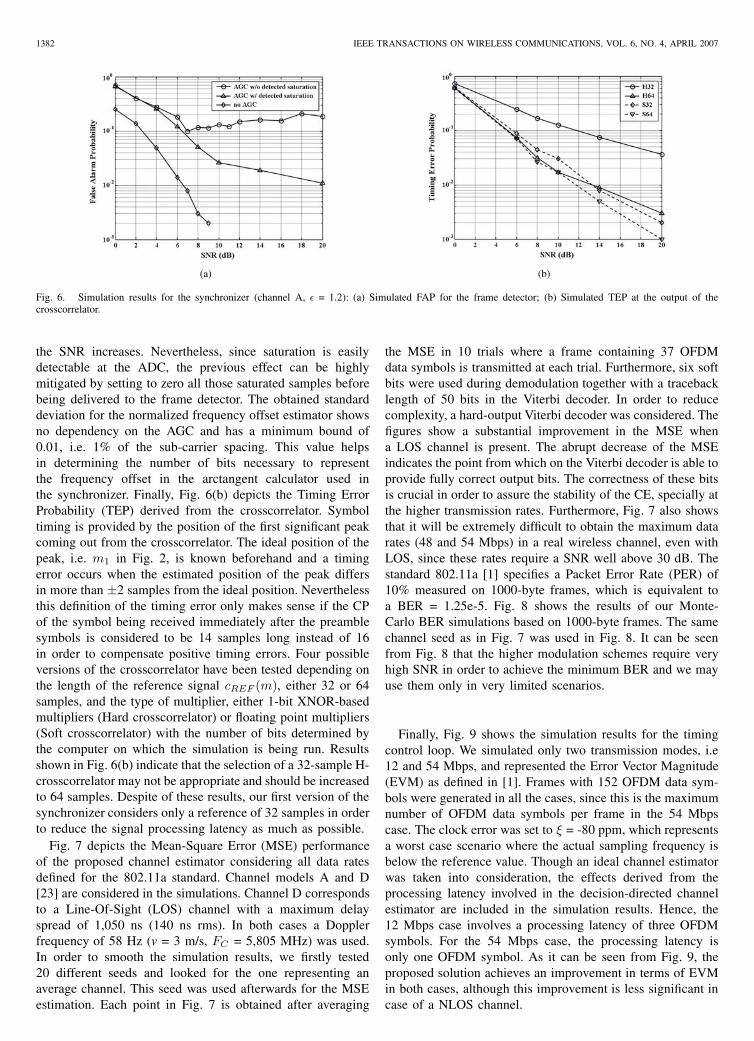
1382 IEEE TRANSACTIONS ON WIRELESS COMMUNICATIONS, VOL. 6, NO. 4, APRIL 2007
(a) (b)
Fig. 6. Simulation results for the synchronizer (channel A, ε = 1.2): (a) Simulated FAP for the frame detector; (b) Simulated TEP at the output of thecrosscorrelator.
the SNR increases. Nevertheless, since saturation is easilydetectable at the ADC, the previous effect can be highlymitigated by setting to zero all those saturated samples beforebeing delivered to the frame detector. The obtained standarddeviation for the normalized frequency offset estimator showsno dependency on the AGC and has a minimum bound of0.01, i.e. 1% of the sub-carrier spacing. This value helpsin determining the number of bits necessary to representthe frequency offset in the arctangent calculator used inthe synchronizer. Finally, Fig. 6(b) depicts the Timing ErrorProbability (TEP) derived from the crosscorrelator. Symboltiming is provided by the position of the first significant peakcoming out from the crosscorrelator. The ideal position of thepeak, i.e. m1 in Fig. 2, is known beforehand and a timingerror occurs when the estimated position of the peak differsin more than ±2 samples from the ideal position. Neverthelessthis definition of the timing error only makes sense if the CPof the symbol being received immediately after the preamblesymbols is considered to be 14 samples long instead of 16in order to compensate positive timing errors. Four possibleversions of the crosscorrelator have been tested depending onthe length of the reference signal cREF (m), either 32 or 64samples, and the type of multiplier, either 1-bit XNOR-basedmultipliers (Hard crosscorrelator) or floating point multipliers(Soft crosscorrelator) with the number of bits determined bythe computer on which the simulation is being run. Resultsshown in Fig. 6(b) indicate that the selection of a 32-sample H-crosscorrelator may not be appropriate and should be increasedto 64 samples. Despite of these results, our first version of thesynchronizer considers only a reference of 32 samples in orderto reduce the signal processing latency as much as possible.
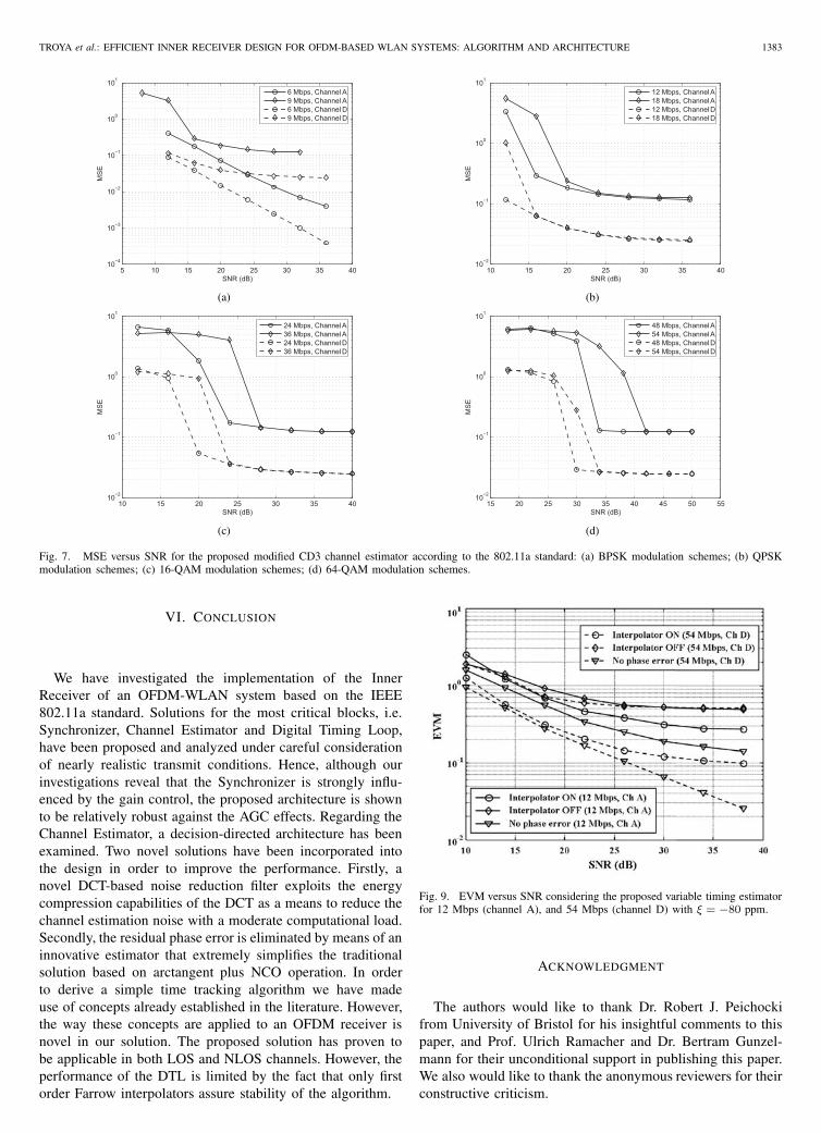
Fig. 7 depicts the Mean-Square Error (MSE) performanceof the proposed channel estimator considering all data ratesdefined for the 802.11a standard. Channel models A and D[23] are considered in the simulations. Channel D correspondsto a Line-Of-Sight (LOS) channel with a maximum delayspread of 1,050 ns (140 ns rms). In both cases a Dopplerfrequency of 58 Hz (v = 3 m/s, FC = 5,805 MHz) was used.In order to smooth the simulation results, we firstly tested20 different seeds and looked for the one representing anaverage channel. This seed was used afterwards for the MSEestimation. Each point in Fig. 7 is obtained after averaging
the MSE in 10 trials where a frame containing 37 OFDMdata symbols is transmitted at each trial. Furthermore, six softbits were used during demodulation together with a tracebacklength of 50 bits in the Viterbi decoder. In order to reducecomplexity, a hard-output Viterbi decoder was considered. Thefigures show a substantial improvement in the MSE whena LOS channel is present. The abrupt decrease of the MSEindicates the point from which on the Viterbi decoder is able toprovide fully correct output bits. The correctness of these bitsis crucial in order to assure the stability of the CE, specially atthe higher transmission rates. Furthermore, Fig. 7 also showsthat it will be extremely difficult to obtain the maximum datarates (48 and 54 Mbps) in a real wireless channel, even withLOS, since these rates require a SNR well above 30 dB. Thestandard 802.11a [1] specifies a Packet Error Rate (PER) of10% measured on 1000-byte frames, which is equivalent toa BER = 1.25e-5. Fig. 8 shows the results of our Monte-Carlo BER simulations based on 1000-byte frames. The samechannel seed as in Fig. 7 was used in Fig. 8. It can be seenfrom Fig. 8 that the higher modulation schemes require veryhigh SNR in order to achieve the minimum BER and we mayuse them only in very limited scenarios.
Finally, Fig. 9 shows the simulation results for the timingcontrol loop. We simulated only two transmission modes, i.e12 and 54 Mbps, and represented the Error Vector Magnitude(EVM) as defined in [1]. Frames with 152 OFDM data sym-bols were generated in all the cases, since this is the maximumnumber of OFDM data symbols per frame in the 54 Mbpscase. The clock error was set to ξ = -80 ppm, which representsa worst case scenario where the actual sampling frequency isbelow the reference value. Though an ideal channel estimatorwas taken into consideration, the effects derived from theprocessing latency involved in the decision-directed channelestimator are included in the simulation results. Hence, the12 Mbps case involves a processing latency of three OFDMsymbols. For the 54 Mbps case, the processing latency isonly one OFDM symbol. As it can be seen from Fig. 9, theproposed solution achieves an improvement in terms of EVMin both cases, although this improvement is less significant incase of a NLOS channel.
TROYA et al.: EFFICIENT INNER RECEIVER DESIGN FOR OFDM-BASED WLAN SYSTEMS: ALGORITHM AND ARCHITECTURE 1383
5 10 15 20 25 30 35 4010−4
10−3
10−2
10−1
100
101
SNR (dB)
MS
E6 Mbps, Channel A9 Mbps, Channel A6 Mbps, Channel D9 Mbps, Channel D
(a)
10 15 20 25 30 35 4010−2
10−1
100
101
SNR (dB)
MS
E
12 Mbps, Channel A18 Mbps, Channel A12 Mbps, Channel D18 Mbps, Channel D
(b)
10 15 20 25 30 35 4010−2
10−1
100
101
SNR (dB)
MS
E
24 Mbps, Channel A36 Mbps, Channel A24 Mbps, Channel D36 Mbps, Channel D
(c)
15 20 25 30 35 40 45 50 5510−2
10−1
100
101
SNR (dB)
MS
E
48 Mbps, Channel A54 Mbps, Channel A48 Mbps, Channel D54 Mbps, Channel D
(d)
Fig. 7. MSE versus SNR for the proposed modified CD3 channel estimator according to the 802.11a standard: (a) BPSK modulation schemes; (b) QPSKmodulation schemes; (c) 16-QAM modulation schemes; (d) 64-QAM modulation schemes.
VI. CONCLUSION
We have investigated the implementation of the InnerReceiver of an OFDM-WLAN system based on the IEEE802.11a standard. Solutions for the most critical blocks, i.e.Synchronizer, Channel Estimator and Digital Timing Loop,have been proposed and analyzed under careful considerationof nearly realistic transmit conditions. Hence, although ourinvestigations reveal that the Synchronizer is strongly influ-enced by the gain control, the proposed architecture is shownto be relatively robust against the AGC effects. Regarding theChannel Estimator, a decision-directed architecture has beenexamined. Two novel solutions have been incorporated intothe design in order to improve the performance. Firstly, anovel DCT-based noise reduction filter exploits the energycompression capabilities of the DCT as a means to reduce thechannel estimation noise with a moderate computational load.Secondly, the residual phase error is eliminated by means of aninnovative estimator that extremely simplifies the traditionalsolution based on arctangent plus NCO operation. In orderto derive a simple time tracking algorithm we have madeuse of concepts already established in the literature. However,the way these concepts are applied to an OFDM receiver isnovel in our solution. The proposed solution has proven tobe applicable in both LOS and NLOS channels. However, theperformance of the DTL is limited by the fact that only firstorder Farrow interpolators assure stability of the algorithm.
Fig. 9. EVM versus SNR considering the proposed variable timing estimatorfor 12 Mbps (channel A), and 54 Mbps (channel D) with ξ = −80 ppm.
ACKNOWLEDGMENT
The authors would like to thank Dr. Robert J. Peichockifrom University of Bristol for his insightful comments to thispaper, and Prof. Ulrich Ramacher and Dr. Bertram Gunzel-mann for their unconditional support in publishing this paper.We also would like to thank the anonymous reviewers for theirconstructive criticism.

1384 IEEE TRANSACTIONS ON WIRELESS COMMUNICATIONS, VOL. 6, NO. 4, APRIL 2007
2 4 6 8 10 12 14 16 1810−6
10−5
10−4
10−3
10−2
10−1
100
SNR (dB)
BE
R6 Mbps, Channel A9 Mbps, Channel A6 Mbps, Channel D9 Mbps, Channel DPER = 10%
(a)
5 7 9 11 13 15 17 19 21 23 2510−6
10−5
10−4
10−3
10−2
10−1
100
SNR (dB)
BE
R
12 Mbps, Channel A18 Mbps, Channel A12 Mbps, Channel D18 Mbps, Channel DPER = 10%
(b)
12 14 16 18 20 22 24 26 28 30 32 34 36 38 4010−6
10−5
10−4
10−3
10−2
10−1
100
SNR (dB)
BE
R
24 Mbps, Channel A36 Mbps, Channel A24 Mbps, Channel D36 Mbps, Channel DPER = 10%
(c)
26 28 30 32 34 36 38 40 42 44 46 48 5010−6
10−5
10−4
10−3
10−2
10−1
100
SNR (dB)
BE
R
48 Mbps, Channel A54 Mbps, Channel A48 Mbps, Channel D54 Mbps, Channel DPER = 10%
(d)
Fig. 8. BER versus SNR for the proposed modified CD3 channel estimator according to the 802.11a standard: (a) BPSK modulation schemes; (b) QPSKmodulation schemes; (c) 16-QAM modulation schemes; (d) 64-QAM modulation schemes.
REFERENCES
[1] “Wireless LAN medium access control (MAC) and physical layer (PHY)specifications: High speed physical layer in the 5 GHz band,” IEEEP802.11a/D7.0, Part II, 1999.
[2] “Wireless LAN medium access control (MAC) and physical layer (PHY)specifications. Amendment 4: Further higher data rate extension in the2.4 GHz band,” IEEE 802.11G. Standard for IT - Telecommunicationsand information exchange between systems LAN/MAN - Part II, 2003.
[3] [Online.] Available: www.wigwam-project.com[4] [Online.] Available: www.multibandofdm.org[5] M. Speth, S. A. Fechtel, G. Fock, and H. Meyr, “Optimum receiver
design for wireless broad-band systems using OFDM - Part I,” IEEETrans. Commun., vol. 47, no. 11, pp. 1668–1677, Nov. 1999.
[6] P. Robertson and S. Kaiser, “Analysis of the effects of phase-noise inorthogonal frequency division multiplex (OFDM) systems,” in Proc.IEEE ICC, June 1995, pp. 1652–1657.
[7] H. Meyr, M. Moeneclaey, and S. Fechtel, Digital CommunicationReceivers: Synchronization, Channel Estimation, and Signal Processing.New York: Wiley, 1998.
[8] M. Krstic, A. Troya, K. Maharatna, and E. Grass, “Optimized low-power synchronizer design for the IEEE 802.11a standard,” in Proc.IEEE ICASSP, Apr. 2003, vol. 2, pp. 333–336.
[9] A. Troya, K. Maharatna, M. Krstic, and E. Grass, “Method and devicefor frame detection and synchronizer.” PCT Patent WO 2004/008706A2, pending, Jan. 22, 2004.
[10] K. Maharatna, A. Troya, S. Banerjee, and E. Grass, “A CORDIC likeprocessor for computation of arctangent and absolute magnitude of avector,” in Proc. IEEE ISCAS, May 2004, vol. 2, pp. 713–716.
[11] K. Maharatna, A. Troya, S. Banerjee, E. Grass, and M. Krstic, “A 16-bitCORDIC rotator for high-speed wireless LAN,” in Proc. IEEE PIMRC,Sep. 2004, vol. 3, pp. 1747–1751.
[12] K. Maharatna, S. Banerjee, E. Grass, M. Krstic, and A. Troya, “Modifiedvirtually scaling-free CORDIC rotator algorithm and architecture,” IEEETrans. Circuits Syst. Video Technol., vol. 15, no. 11, pp. 1463–1474, Nov.2005.
[13] T. M. Schmidl and D. C. Cox, “Robust frequency and timing synchro-nization for OFDM,” IEEE Trans. Commun., vol. 45, no. 12, pp. 1613–1621, Dec. 1997.
[14] B. Stantchev and G. Fettweis, “Burst synchronization for OFDM-basedcellular systems with separate signaling channel,” in Proc. IEEE VTC,May 1998, pp. 758–762.
[15] V. Mignone and A. Morello, “CD3-OFDM: A novel demodulationscheme for fixed and mobile receivers,” IEEE Trans. Commun., vol.44, no. 9, pp. 1144–1151, Sep. 1996.
[16] J.-J. van de Beek, O. Edfors, M. Sandell, S. K. Wilson, and P. O. Bör-jesson, “On channel estimation in OFDM systems,” in Proc. IEEE VTC,July 1995, vol. 2, pp. 815–819.
[17] O. Edfors, M. Sandell, J.-J. van de Beek, S. K. Wilson, and P. O. Bör-jesson, “OFDM channel estimation by singular value decomposition,”IEEE Trans. Commun., vol. 46, no. 7, pp. 931–939, July 1998.
[18] H. Schmidt, V. Kühn, K.-D. Kammeyer, R. Rueckriem, and S. Fechtel,“Channel tracking in wireless OFDM systems,” in Proc. 5th WorldMulti-Conference on Systemics, Cybernetics and Informatics, July 2001,vol. 4, pp. 402–406.
[19] A. Troya, M. Krstic, and K. Maharatna, “Simplified residual phasecorrection mechanism for the IEEE 802.11a standard,” in Proc. IEEEVTC-Fall, Oct. 2003, vol. 2, pp. 1137–1141.
[20] A. Troya, K. Maharatna, and M. Krstic, “Verfahren und Vorrichtung zurFehlerkorrektur von Multiplex-Signalen.” PCT Patent WO 2004/036863A1, pending, Apr. 29, 2004.
[21] B. Yang, K. B. Letaief, R. S. Cheng, and Z. Cao, “An improvedcombined symbol and sampling clock synchronization method forOFDM systems,” in Proc. IEEE Wireless Commun. Networking Conf.,Sep. 1999, vol. 3, pp. 1153–1157.
[22] L. Erup, F. M. Gardner, and R. A. Harris, “Interpolation in digitalmodems - Part II: Implementation and performance,” IEEE Trans.Commun., vol. 41, no. 6, pp. 998–1008, June 1993.
[23] “Criteria for comparison,” ETSI Technical Report 30701F, BRAN WG3PHY Subgroup, May 1998.

TROYA et al.: EFFICIENT INNER RECEIVER DESIGN FOR OFDM-BASED WLAN SYSTEMS: ALGORITHM AND ARCHITECTURE 1385
Alfonso Troya (M’95) was born in Barcelona,Spain, in 1975. He received the M.Sc. degree inTelecommunications Engineering from the Techni-cal University of Catalonia, Barcelona, Spain, in1999, and the Dr.-Ing. degree from BrandenburgUniversity of Technology, Cottbus, Germany, in2004.
He joined the IHP (Institute for High Performancemicroelectronics), Frankfurt (Oder), Germany, in1999, as a Research Associate in the Wireless Com-munication Systems Department, where he worked
on the development and implementation of digital signal processing algo-rithms for broadband wireless communication systems. In October 2004he joined Infineon Technologies AG, Munich, Germany, as an AlgorithmConcept Engineer. He is currently involved in the development of OFDM-based communication systems and their implementation on Software-DefinedRadio architectures.
Dr. Troya is a member of the IEEE Signal Processing Society.
Koushik Maharatna (M’02) received the M.Sc. de-gree in Electronic Science from Calcutta University,Calcutta, India, in 1995 and the Ph.D. degree fromJadavpur University, Calcutta, India, in 2002. From1996 to 2000, he was involved in projects sponsoredby the Government of India undertaken at the In-dian Institute of Technology (IIT), Kharagpur, India.From 2000 to 2003, he was a Research Scientist withIHP, Frankfurt (Oder), Germany. During this phase,his main involvement was related to the design of asingle-chip modem for the IEEE 802.11a standard.
In August 2003, he joined the Department of Electrical & ElectronicsEngineering, University of Bristol, Bristol, UK as a Lecturer. From October2006 he is with the School of Electronics and Computer Science, University ofSouthampton, where he is currently a Senior Lecturer. His research interestsinclude development of VLSI architectures for the application in DSP andcommunication, computer arithmetic, low-power design, and analog signalprocessing.
Dr. Maharatna has served as session chair for IEEE ISCAS 2005 andVLSI design Conference 2006, and also acted as a reviewer for several IEEEJournals and Conferences. He is currently a member of the Engineering andPhysical Research Council (EPSRC) college in the UK. He is a member ofthe IEEE Circuits and Systems Society.
Milos Krstic was born in Nis, Serbia, in 1973.He received the Dipl.-Ing. and the M.Sc. degreesin Electronics from the University of Nis, Serbia,in 1997 and 2001, respectively, and the Dr.-Ing.degree from Brandenburg University of Technology,Cottbus, Germany, in 2006.
Since 2001 he has been with IHP, Frankfurt(Oder), Germany, as a Research Associate withinthe Wireless Communication Systems Department,where he is currently working on low-power digi-tal design techniques for wireless applications and
globally-asynchronous locally-synchronous (GALS) methodologies for digitalsystems integration.
Eckhard Grass received his Dr.-Ing. degree inElectronics from the Humboldt University, Berlin,Germany, in 1992.
He worked as a Visiting Research Fellow atLoughborough University (U.K.) from 1993 to 1995and as a Senior Lecturer in Microelectronics at theUniversity of Westminster, London, U.K., from 1995to 1999. He has been with IHP, Frankfurt (Oder),Germany, since 1999, where he currently leads aproject on the development and implementation ofa wireless broadband communication system in the
60 GHz band. His research interests include data-driven (asynchronous) signalprocessing structures and low-power VLSI implementation of communicationsystems.
Ulrich Jagdhold received the Diploma in Physics(M.Sc. degree) from the Technical University ofDresden, Dresden, Germany, in 1987. From 1987 to1996, he was with the Technology Integration Groupof the IHP, Frankfurt (Oder), Germany, workingon CMOS, BiCMOS, and SiGe technologies anddevice physics. In 1997 he joined the WirelessCommunication Systems Department of IHP, wherehe has been working on WLAN system developmentprojects, focusing on baseband integration issuesand ASIC design, including development of digital
CMOS libraries.
Rolf Kraemer (M’79) received his Diploma andPh.D. degrees in Electrical Engineering and Com-puter Science from the RWTH Aachen, Germany,in 1979 and 1985, respectively. He has worked for15 years in R&D of communication and multimediasystems at Philips Research Laboratories in Ham-burg and Aachen. Since 1998 he is a professor ofsystems at the Brandenburg University of Technol-ogy, Cottbus, Germany. He also leads the WirelessCommunications Systems Department of the IHP,where his research focus is on wireless Internet
systems spanning from application down to Systems-on-Chip. He is co-founder of the startup company lesswire AG, where he holds the positionof the CTO.
Prof. Kraemer has published over 150 conference and journal papers, andholds 16 international patents. He is a member of the IEEE Computer Society,the VDE-NTG, and the German Informatics Society.