Effects of Varied Cleaning Methods on Ni-5% W Substrate
17
Nanomaterials 2012, 2, 251-267; doi:10.3390/nano2030251 nanomaterials ISSN 2079-4991 www.mdpi.com/journal/nanomaterials Article Effects of Varied Cleaning Methods on Ni-5% W Substrate for Dip-Coating of Water-based Buffer Layers: An X-ray Photoelectron Spectroscopy Study Vyshnavi Narayanan 1, *, Els Bruneel 1 , Ruben Hühne 2 and Isabel Van Driessche 1 1 Sol-Gel Centre for Research on Inorganic Powders and Thin Film Synthesis SCRiPTS, Department of Inorganic and Physical Chemistry, Ghent University, Krijgslaan 281-S3, Gent B-9000, Belgium; E-Mails: [email protected] (E.B.); [email protected] (I.V.D.) 2 IFW Dresden, Helmholtzstrasse 20, Dresden 01069, Germany; E-Mail: [email protected] * Author to whom correspondence should be addressed; E-Mails: [email protected]; [email protected]; Tel.: +32-(0)-9-264-44-33; Fax: +32-(0)-9-264-49-83. Received: 31 May 2012; in revised form: 17 July 2012 / Accepted: 25 July 2012 / Published: 9 August 2012 Abstract: This work describes various combinations of cleaning methods involved in the preparation of Ni-5% W substrates for the deposition of buffer layers using water-based solvents. The substrate has been studied for its surface properties using X-ray photoelectron spectroscopy (XPS). The contaminants in the substrates have been quantified and the appropriate cleaning method was chosen in terms of contaminants level and showing good surface crystallinity to further consider them for depositing chemical solution-based buffer layers for Y 1 Ba 2 Cu 3 O y (YBCO) coated conductors. Keywords: X-ray photoelectron spectroscopy; cleaning of Ni-5% W substrate; depth profile studies; thin films and coatings 1. Introduction Second generation superconductors employing RABiTS (Rolling-Assisted-Biaxially-Textured-Substrates) offer a viable way to develop superconductor wires for commercial use. Coated conductors are based on the deposition of (0 0 l) oriented buffer layers and the c-axis oriented YBa 2 Cu 3 O 7−x (YBCO) films on these nickel alloy substrates. Researchers have noticed that the surface properties of the nickel surface play a crucial role in making it conducive to epitaxial film deposition [1]. The crucial factor to OPEN ACCESS
Transcript of Effects of Varied Cleaning Methods on Ni-5% W Substrate

Nanomaterials 2012, 2, 251-267; doi:10.3390/nano2030251
nanomaterialsISSN 2079-4991
www.mdpi.com/journal/nanomaterials
Article
Effects of Varied Cleaning Methods on Ni-5% W Substrate for Dip-Coating of Water-based Buffer Layers: An X-ray Photoelectron Spectroscopy Study
Vyshnavi Narayanan 1,*, Els Bruneel 1, Ruben Hühne 2 and Isabel Van Driessche 1
1 Sol-Gel Centre for Research on Inorganic Powders and Thin Film Synthesis SCRiPTS, Department
of Inorganic and Physical Chemistry, Ghent University, Krijgslaan 281-S3, Gent B-9000, Belgium;
E-Mails: [email protected] (E.B.); [email protected] (I.V.D.) 2 IFW Dresden, Helmholtzstrasse 20, Dresden 01069, Germany; E-Mail: [email protected]
* Author to whom correspondence should be addressed; E-Mails: [email protected];
[email protected]; Tel.: +32-(0)-9-264-44-33; Fax: +32-(0)-9-264-49-83.
Received: 31 May 2012; in revised form: 17 July 2012 / Accepted: 25 July 2012 /
Published: 9 August 2012
Abstract: This work describes various combinations of cleaning methods involved in the
preparation of Ni-5% W substrates for the deposition of buffer layers using water-based
solvents. The substrate has been studied for its surface properties using X-ray
photoelectron spectroscopy (XPS). The contaminants in the substrates have been quantified
and the appropriate cleaning method was chosen in terms of contaminants level and
showing good surface crystallinity to further consider them for depositing chemical
solution-based buffer layers for Y1Ba2Cu3Oy (YBCO) coated conductors.
Keywords: X-ray photoelectron spectroscopy; cleaning of Ni-5% W substrate; depth
profile studies; thin films and coatings
1. Introduction
Second generation superconductors employing RABiTS (Rolling-Assisted-Biaxially-Textured-Substrates)
offer a viable way to develop superconductor wires for commercial use. Coated conductors are based
on the deposition of (0 0 l) oriented buffer layers and the c-axis oriented YBa2Cu3O7−x (YBCO) films
on these nickel alloy substrates. Researchers have noticed that the surface properties of the nickel
surface play a crucial role in making it conducive to epitaxial film deposition [1]. The crucial factor to
OPEN ACCESS

Nanomaterials 2012, 2
252
obtain a superconducting YBCO thin film is dependent on the ability to deposit smooth, dense,
crack-free and highly aligned oxide buffer layers on textured metal substrates to protect the
superconductors from metal contamination and, to provide an appropriate biaxially oriented, lattice
matched substrate for the subsequent epitaxial growth of superconducting YBCO on top of it.
Furthermore, such a barrier layer may also limit diffusion as well from the metal substrate to the
superconducting coating as inversely, thereby allowing a better control of purity and oxygen content.
Before a buffer layer can be deposited, the substrates must be prepared for coating by an optimized
cleaning procedure. Subsequently, optimized buffer layer architectures must be designed in order to
have a biaxially textured, smooth and dense thin film that fulfills all the requirements. Many buffer
layers including CeO2, doped CeO2, YSZ, La2Zr2O7, Gd2Zr2O7, LaxCe1−xOδ have been prevalently
used for the support of YBCO growth [2–13]. Our work was focused on depositing water based buffer
layers using chemical solution deposition method (CSD) on the Ni-5% W substrates. Water-based
methods were considered because of their effectiveness based on environmental and economic
reasons [7–15]. Since water-based solutions possess a quite high surface tension, an optimal way of
preparing the substrate to get a uniform coating on top of it was a challenge in its own way. Following
this, different cleaning methods with inclusion of chemicals had to be considered in order to improve
wetting behavior. However, inclusion of chemicals can add-up to the already present impurities on the
substrates in the form of carbon from the atmosphere. Moreover, grease and oil is used while rolling
the substrates during its preparation for obtaining epitaxial RABiTS Ni-5% W substrates. This can also
add to the level of carbon contaminations. Additionally, the substrates can be covered by a passivating
layer of NiO on top, which can prove detrimental for the to-be deposited buffer layers in terms of
transferring the epitaxy. Therefore, a suitable and convincing cleaning method had to be chosen and
more fundamental insights on the surface behavior had to be gained.
Previously, there have been a few reports on different cleaning methods used for the preparation of
Ni-5% W substrates for coating the buffer layers using CSD [6,10,11,16]. Sathyamurthy et al. [16]
examined the effect of a chemical etching process on the amount of carbon and oxygen contamination
on the nickel surface.
In this work, the focus has been directed towards elucidation of the action of different cleaning
methods on the Ni-5 at % W substrates, including a thermal treatment to make it suitable for coating of
aqueous based buffer layers. The results obtained from a combination of a chemical and thermal
cleaning procedure based on a sequence of chemical treatments in trichloroethylene, acetone,
methanol, deionized water and an etching mixture of hydrogen peroxide and formic acid and thermal
treatment at 800 °C are reported. The chemical composition in terms of atom percentages of Ni and W
and the contaminants including C and O quantified using XPS is presented. Previously, XPS has been
used as an effective analytical tool for studying the buffer layer capacity [17]. The wetting property of
the substrate after different cleaning methods has been pictured and presented. It was found that the
cleaning treatment significantly improves the wettability of the substrates, a crucial property for the
epitaxial growth of crack-free and homogeneous buffer layers by means of water-based solution-gel
deposition techniques.
Nanomaterials 2012, 2
253
2. Experimental Section
Flexible 80 µm thick and polished substrates were provided by D-Nano GmbH and produced by
evico GmbH. They have been considered for investigation throughout this work.
2.1. Chemical Cleaning with Etching Process
The substrates were dipped consecutively in trichloroethylene 99% (Acros Organics), in acetone
99.5% (Fiers) and in methanol 99.85% (Fiers), each dipping step lasted for 5 min. This was
carried-out in order to remove organic traces of oil, grease, and also dirt which can occur due to their
use in rolling process of the RABiTS Ni-5%W substrate. This degreasing procedure was followed by a
5 min rinse in MiliQ water obtained from a MILLIPORE 00A/040 MiliQ water purification system. In
this step, residual solvents and ionic salts were removed. Subsequently, the substrates were introduced
in a hot mixture (50–55 °C) 50 vol % each of hydrogen peroxide (H2O2) 35% in weight (Sigma
Aldrich) and formic acid (HCOOH) 99% (Chem-Lab), for 15 min. This final step will involve “etching”
of the surface, more precisely the grain boundaries. Substrates were finally rinsed twice for 10 min
with MiliQ water. This whole sequence of the treatment is called “chemical cleaning with etching”
of substrates.
2.2. Thermal Cleaning Process
In the “thermal cleaning process” substrates were exposed to high temperatures (800 °C) for 1 h in a
quartz tubular furnace (Carbolite, Three zone furnace) and in a reducing atmosphere provided by a
continuous flow of Ar-5% H2 gas maintained at 0.2 L/min. The native NiO, which can act as passive
protection for the Ni-5% W substrates will be reduced under the reducing gas flow during this step.
Heating and cooling rate was set at 10 °C/min. After this thermal treatment the substrates were stored
in methanol to avoid contamination from air and particulates in the atmosphere.
2.3. XPS Characterization
The contaminants, such as carbon and oxygen (as NiO), present in the tapes under uncleaned and
differently cleaned conditions were evaluated by XPS depth profiling (S-probe, Surface Science
Instruments, VG with a monochromatic AlKα-source, 1,486.6 eV). The voltage and power of the
source were kept constant at 10 KV, 200 W. Sputtering of an area of 3 × 3 mm2 was performed with an
Ar+-ion gun (4 keV). After each consecutive sputter cycle an area of 250 × 1000 µm2 was analyzed
with an hemispherical analyzer. Regions for O 1s, C 1s, Ni 2p and W 4f peaks were registered with a
resolution of 0.15 eV. Peak areas were converted into atomic concentrations with the software package
CasaXPS (Casa Software Ltd., UK) using a Shirley background and Scoffield sensitivity factors.
Ar+-ion sputtering was carried-out for four consecutive sputter cycles each lasting 10 s. In total, 40 s of
sputtering was carried out. According to the standard sputtering rate of Ta2O5, fixed at 0.15 nm/s, each
sputter cycle can be roughly estimated to remove 1.5 nm thickness of the substrate and in total,
therefore approximately 6 nm thickness of the substrate is believed to have been sputtered
and removed.

Nanomaterials 2012, 2
254
The XPS study was supported by a reflection high energy electron diffraction (RHEED) analysis.
RHEED is an electron diffraction technique used to characterize the topmost layer (2–5 nm) of a
material. A focused beam of electrons, generated by an electron gun, strikes the surface of the sample
under a grazing angle (<1.5°). The electrons are diffracted by the atoms at the sample’s surface. Due to
the very small angle and a wavelength of 7.08 nm for an accelerating potential of 30 keV, their mean
free path perpendicular to the surface is 5 to 10 nm at the most. Typically, the electrons penetrate small
islands at a rough surface, which leads to a transmission pattern similar to transmission electron
microscopy. The diffraction pattern, captured on a photo luminescent screen with an additional CCD
camera, as a result exhibits either discrete spots (for a highly oriented material) or spots merged into
rings (for polycrystalline material). The as-received and cleaned Ni-5% W substrates were analyzed
using a STAIB RHEED instrument at the IFW Dresden, Germany. The top surface crystallinity with
diffraction spots corresponding to epitaxial metallic Ni is crucial for the further deposition of buffer
layers to grow c-axis oriented superconducting YBCO.
3. Results and Discussion
In the following discussion, different combinations of chemical and thermal cleaning were
carried-out on the substrates and have been analyzed using XPS.
3.1. Uncleaned Ni-5% W Substrate
Figure 1 shows the depth profile XPS-study of the as-received, uncleaned substrate. The top surface
shows a significant carbon contamination. The native carbon and oxygen contamination is removed
after 10 s of sputtering, exposing the Ni and W peaks.
Figure 1. X-ray photoelectron spectroscopy (XPS) depth profile studies of uncleaned
Ni-5% W substrate.
0
10
20
30
40
50
60
70
80
90
100
0 10 20 30 40 50
Ato
m p
erc
ent
Sputtering time(s)
Carbon 1s
Nickel 2p
Oxygen 1s
Tungsten 4f

Nanomaterials 2012, 2
255
Figure 2 explicitly depicts the Ni peaks under different sputtering cycles (from bottom to top). The
Ni peaks in different sputtering cycle are shown. The top-surface exposing the epitaxial Ni is crucial
for the epitaxial growth of the following buffer layers and YBCO growth. The intensity of Ni peaks on
the top surface and in different depths of sputtering, correlates to the exposed epitaxial Ni surface. The
intense Ni peaks using XPS (AlKα): Ni 2p3/2 and Ni 2p1/2 for metallic Ni is expected at a binding
energy of 852.3 eV and 869.7 eV (along with their corresponding satellite peaks) whereas, it is
expected at 853.3 eV and 871.7 eV for NiO. Normally, any observation of a broader and shifted peak
at 853.3 eV can be correlated to the presence of NiO. Additionally, a peak shift in Ni peaks helps in
verifying whether it corresponds to metallic Ni or that of NiO.
Figure 2. XPS depth profile studies of Ni peaks in uncleaned substrates.
As seen in Figure 2, almost no Ni is visible on the top-surface (0 s of sputtering). After sputtering
Ni peaks can be correlated to the corresponding metallic Ni peak position as observed from the figure.
The reason for the less intense peak of Ni can be attributed to the presence of surface carbon and
oxygen as shown in Figure1. This shows the necessity of cleaning the surface prior to deposition of the
Binding energy (eV)
Inte
nsity
(cps
)
10 s
Top surface at 0 s
20 s
30 s
40 s
Ni 2p1/2
Ni 2p3/2

Nanomaterials 2012, 2
256
buffer layers. The wettability of the substrate was evaluated by measuring the contact angle of water. It
can be seen that, the water droplet did not wet the substrate, instead it remained stagnant with a contact
angle of >75° (Figure 3). This also means that the wettability of the native substrate needs to be
improved in order to coat it using water-based solutions [9,13].
Figure 3. Non-wetting droplet of water on top of uncleaned Ni-5% W substrate.
3.2. Chemical Cleaning with Etching for 15 min
The as-received substrates were chemically cleaned and etched for 15 min. Figure 4 depicts the
various percentages of elements present in this sample after different sputter cycles, starting from the
top-surface. On the surface of the sample a relatively high amount of oxygen was observed. This can
be attributed to the use of the HCOOH-H2O2 mixture which releases active oxygen species that can
attach to the surface of the sample.
Figure 4. XPS depth profile studies of Ni-5% W substrate chemically cleaned with etching
for 15 min.
SubstrateWater droplet75o
0
10
20
30
40
50
60
70
80
90
100
0 10 20 30 40 50
Ato
m p
erc
ent
Sputtering time (s)
Carbon 1s
Nickel 2p
Oxygen 1s
Tungsten 4f

Nanomaterials 2012, 2
257
From Figure 4, the presence of oxygen can be seen even after 20 s of sputtering which indicates that
the etchant has penetrated several nanometres deep into the substrate. From this we can conclude that
the oxidation of the substrate up to ~4.5 nm thickness has occurred. The oxygen peaks, seen in Figure
4 after 10 s of sputtering, is indexed to be partially corresponding to that of NiO. Growth along the
(111) phase is thermodynamically favorable for NiO. This is highly undesirable because it can induce
growth of the buffer layer with a similar orientation, thus hampering the growth of c-axis oriented
superconducting YBCO. Figure 5 shows the Ni-peak after different sputtering cycles.
Figure 5. XPS depth profile studies of Ni peaks in substrate chemically cleaned with
etching for 15 min (with deconvolution for the presence of NiO).
Compared to uncleaned substrate, there is a higher amount of Ni that is exposed on the top-surface
after this cleaning procedure. Also, a decrease in amount of C at the surface can be seen as compared
to that of the uncleaned substrate (Figure 4 vs. Figure 1). The Ni 2p3/2 peak has been deconvoluted
according to the guidelines of Biesinger et al. [18] with peaks for metallic and oxidized Ni, as well as
for their satellites, From this graph we can see that the top surface is predominantly composed of
Binding energy (eV)
Inte
nsity
(cps
)
10 s
Top surface at 0 s
20 s
30 s
40 s
Ni 2p1/2
Ni 2p3/2
Satellite peaks
Oxides of Ni
Ni Metal
Nanomaterials 2012, 2
258
oxidized Nickel with a peak at higher binding energies (above 853 eV), while with sputtering the peak
at higher binding energies diminishes and the fraction of metallic Ni increases.
Additionally, it can be seen that, after etching, the concentration of carbon has decreased in
comparison to uncleaned substrates (although the oxygen percentage is higher). This signifies that the
carbon impurities are removed after etching. On the other hand, the oxygen percentage remained high,
showing the formation of NiO as stated before, which is very much undesirable.
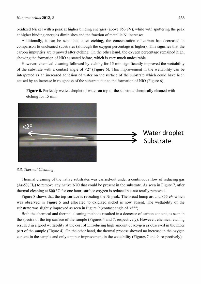
However, chemical cleaning followed by etching for 15 min significantly improved the wettability
of the substrate with a contact angle of <2° (Figure 6). This improvement in the wettability can be
interpreted as an increased adhesion of water on the surface of the substrate which could have been
caused by an increase in roughness of the substrate due to the formation of NiO (Figure 6).
Figure 6. Perfectly wetted droplet of water on top of the substrate chemically cleaned with
etching for 15 min.
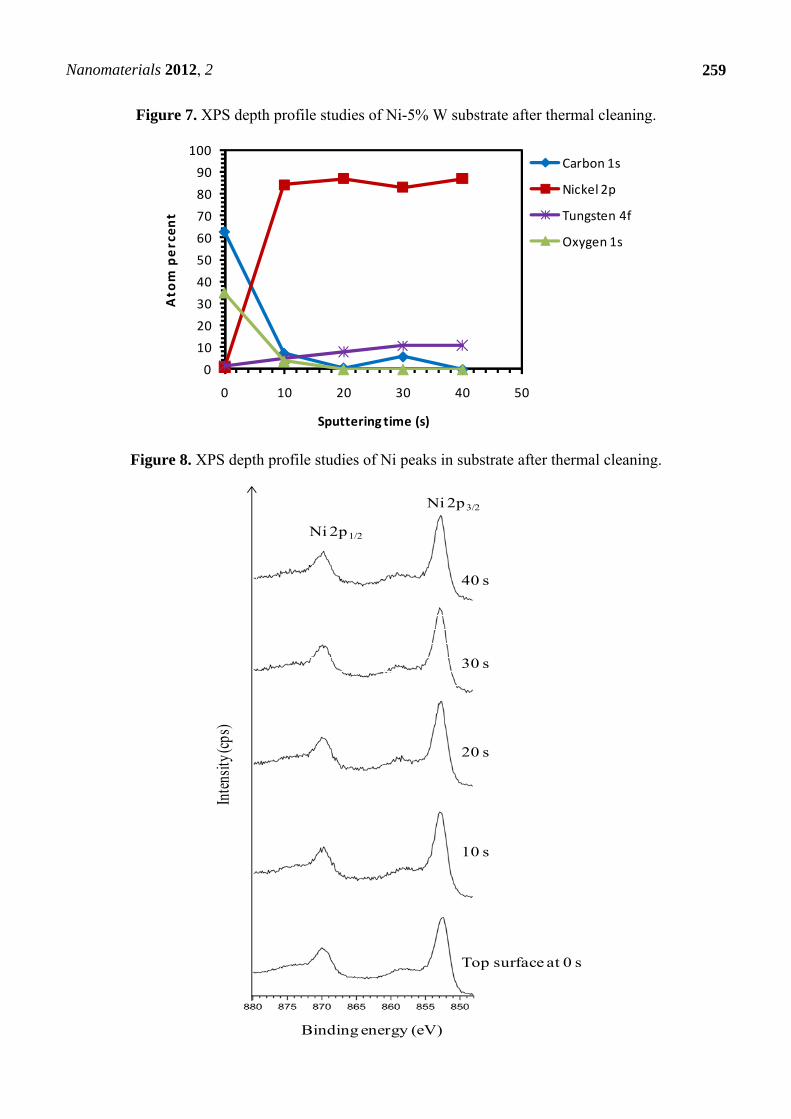
3.3. Thermal Cleaning
Thermal cleaning of the native substrates was carried-out under a continuous flow of reducing gas
(Ar-5% H2) to remove any native NiO that could be present in the substrate. As seen in Figure 7, after
thermal cleaning at 800 °C for one hour, surface oxygen is reduced but not totally removed.
Figure 8 shows that the top-surface is revealing the Ni peak. The broad hump around 855 eV which
was observed in Figure 5 and allocated to oxidized nickel is now absent. The wettability of the
substrate was slightly improved as seen in Figure 9 (contact angle of <55°).
Both the chemical and thermal cleaning methods resulted in a decrease of carbon content, as seen in
the spectra of the top surface of the sample (Figures 4 and 7, respectively). However, chemical etching
resulted in a good wettability at the cost of introducing high amount of oxygen as observed in the inner
part of the sample (Figure 4). On the other hand, the thermal process showed no increase in the oxygen
content in the sample and only a minor improvement in the wettability (Figures 7 and 9, respectively).
SubstrateWater droplet
<2o
Nanomaterials 2012, 2
259
Figure 7. XPS depth profile studies of Ni-5% W substrate after thermal cleaning.
Figure 8. XPS depth profile studies of Ni peaks in substrate after thermal cleaning.
0
10
20
30
40
50
60
70
80
90
100
0 10 20 30 40 50
Ato
m p
erc
ent
Sputtering time (s)
Carbon 1s
Nickel 2p
Tungsten 4f
Oxygen 1s
Binding energy (eV)
Inte
nsity
(cps
)
10 s
Top surface at 0 s
20 s
30 s
40 s
Ni 2p1/2
Ni 2p3/2

Nanomaterials 2012, 2
260
Figure 9. Water droplet on top of a thermally cleaned Ni-5% W substrate.
3.4. Thermal Cleaning Followed by Chemical Cleaning with Etching for 15 min
To ensure good wettability of the surface the above said sequence of thermal treatment was
followed by chemical cleaning and etching. This process resulted in an improvement in the wettability
with a contact angle of <5°, but the contamination with NiO did not improve as seen in Figures 10 and 11.
Figure 10. XPS depth profile studies of Ni-5% W substrate after thermal cleaning followed
by chemical cleaning with etching for 15 min.
SubstrateWater droplet<55o
0
10
20
30
40
50
60
70
80
90
100
0 10 20 30 40 50
Ato
m p
erc
ent
Sputtering time(s)
Carbon 1s
Nickel 2p
Tungsten 4f
Oxygen 1s
Nanomaterials 2012, 2
261
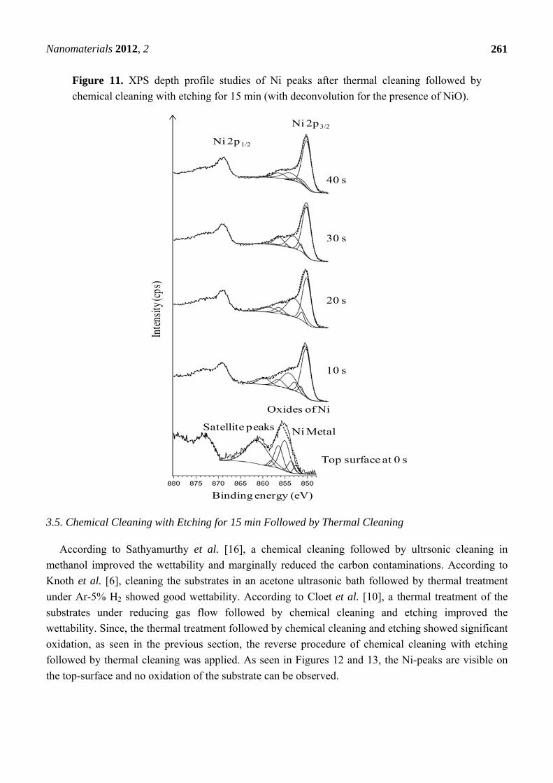
Figure 11. XPS depth profile studies of Ni peaks after thermal cleaning followed by
chemical cleaning with etching for 15 min (with deconvolution for the presence of NiO).
3.5. Chemical Cleaning with Etching for 15 min Followed by Thermal Cleaning
According to Sathyamurthy et al. [16], a chemical cleaning followed by ultrsonic cleaning in
methanol improved the wettability and marginally reduced the carbon contaminations. According to
Knoth et al. [6], cleaning the substrates in an acetone ultrasonic bath followed by thermal treatment
under Ar-5% H2 showed good wettability. According to Cloet et al. [10], a thermal treatment of the
substrates under reducing gas flow followed by chemical cleaning and etching improved the
wettability. Since, the thermal treatment followed by chemical cleaning and etching showed significant
oxidation, as seen in the previous section, the reverse procedure of chemical cleaning with etching
followed by thermal cleaning was applied. As seen in Figures 12 and 13, the Ni-peaks are visible on
the top-surface and no oxidation of the substrate can be observed.
Binding energy (eV)
Inte
nsity
(cps
)
10 s
Top surface at 0 s
20 s
30 s
40 s
Ni 2p1/2
Ni 2p3/2
Satellite peaks
Oxides of Ni
Ni Metal

Nanomaterials 2012, 2
262
Figure 12. XPS depth profile studies of Ni-5% W substrate after chemical cleaning with
etching for 15 min followed by thermal cleaning.
Figure 13. XPS depth profile studies of Ni peaks after chemical cleaning with etching for
15 min followed by thermal cleaning.
0
10
20
30
40
50
60
70
80
90
100
0 10 20 30 40 50
Ato
m p
erc
ent
Sputtering time (s)
Carbon 1s
Nickel 2p
Tungsten 4f
Oxygen 1s
Binding energy (eV)
Inte
nsity
(cps
)
10 s
Top surface at 0 s
20 s
30 s
40 s
Ni 2p1/2
Ni 2p3/2

Nanomaterials 2012, 2
263
3.6. RHEED Analysis
Since top-surface crystallinity is crucial for epitaxial growth of the buffer layers and the YBCO
layer thereon, the substrates were analyzed by RHEED after different cleaning procedures. Therefore,
an uncleaned substrate, a substrate with thermal followed by chemically cleaning with etching and the
substrate with chemical cleaning with etching followed by thermal cleaning was analyzed. The
samples were aligned in such a way that the electron beam was parallel to the <100> or <110>
direction of the cube textured Ni-5% W tape (Figure 14).
Figure 14. Reflection high energy electron diffraction (RHEED) pattern of uncleaned and
differently cleaned Ni-5% W substrate.
As received Ni-5% W Ni-5% W with thermal + chemical treatment
Ni-5% W with chemical + thermal treatment
Vie
w II
<10
0>
Vie
w II
<11
0>
The untreated RABiTS Ni-5% W tape shows only a diffuse diffraction pattern indicating an
amorphous or nanocrystalline surface structure. Such patterns are typically observed on these
substrates as a thin nanocrystalline untextured NiO is building up during storage even at room
temperature. As a result, no crystalline RHEED spots from the Ni tape itself are observed. In contrast,
both of the cleaned Ni-5% W tapes exhibit crystalline diffraction spots. The spots are clearly visible on
the substrate after the thermal followed by chemical cleaning and somewhat more diffuse on the
sample treated with an opposite cleaning sequence. The RHEED diffraction pattern was recalculated
and indexed using software based on a kinematic diffraction theory in order to get information on the
crystal structure of the surface layer. The results were compared to the measured pattern (Figure 15).
Nanomaterials 2012, 2
264
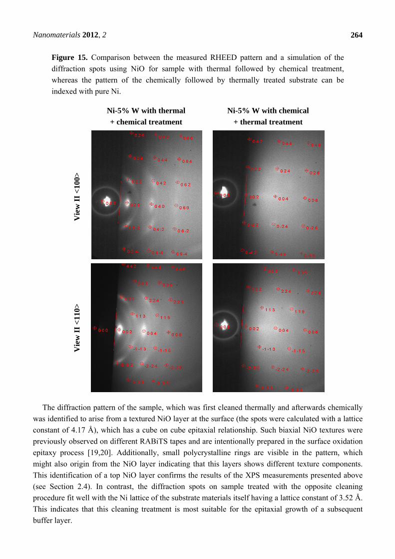
Figure 15. Comparison between the measured RHEED pattern and a simulation of the
diffraction spots using NiO for sample with thermal followed by chemical treatment,
whereas the pattern of the chemically followed by thermally treated substrate can be
indexed with pure Ni.
Ni-5% W with thermal + chemical treatment
Ni-5% W with chemical + thermal treatment
Vie
w II
<10
0>
Vie
w II
<11
0>
The diffraction pattern of the sample, which was first cleaned thermally and afterwards chemically
was identified to arise from a textured NiO layer at the surface (the spots were calculated with a lattice
constant of 4.17 Å), which has a cube on cube epitaxial relationship. Such biaxial NiO textures were
previously observed on different RABiTS tapes and are intentionally prepared in the surface oxidation
epitaxy process [19,20]. Additionally, small polycrystalline rings are visible in the pattern, which
might also origin from the NiO layer indicating that this layers shows different texture components.
This identification of a top NiO layer confirms the results of the XPS measurements presented above
(see Section 2.4). In contrast, the diffraction spots on sample treated with the opposite cleaning
procedure fit well with the Ni lattice of the substrate materials itself having a lattice constant of 3.52 Å.
This indicates that this cleaning treatment is most suitable for the epitaxial growth of a subsequent
buffer layer.

Nanomaterials 2012, 2
265
In summary, the combination of chemical cleaning with etching for 15 min followed by thermal
cleaning was chosen to be the best in terms of a reduced surface contamination, an undisturbed
textured Ni surface and an improved wettability with a contact angle of 18° which is sufficient for
dipcoating in an aqueous sol-gel system [17]. Such cleaned substrates are particularly suitable for
water-based solutions, which have a high surface tension.
4. Conclusions
Different ways of cleaning the Ni-5% W substrate were tested. The contaminations of the surface in
terms of carbon and oxygen were quantified using XPS and the best cleaning method was chosen
based on a minimal contamination, and good surface wettability. Thus a chemical cleaning with
etching for 15 min followed by thermal cleaning is preferred. This procedure results a in minimal
contamination of the top-surface with carbon impurities and NiO, while providing a contact angle
of <20°. An additional RHEED study on this substrate showed diffraction spots corresponding to cube
textured Ni indicating a clean substrate surface. This is an important prerequisite for an epitaxial
growth of buffer layers, in particular for the application of water-based precursor solutions.
Acknowledgments
The authors would like to thank the Belgian Science policy for funding the project under the project
grant P2/00/03 (CHEMAT), IAP/VI-17 (INANOMAT) and FP7-NMP-2007-SMALL-1 grant
No. 205854 (EFECTS). Due thanks are to Olivier Janssens (Ghent University) for the SEM
measurements, Nico De Roo (Ghent University) for assistance with the XPS experiments and Michael
Bäcker (D-Nano GmbH) for providing Ni-5% W tapes. We gratefully acknowledge Sebastian Fähler
for the use of his RHEED analysis software and S. Sathyamurthy for useful discussions.
References
1. Goyal, A.; Norton, D.P.; Christen, D.K.; Specht, E.D.; Paranthaman, M.; Kroeger, D.M.;
Budai, J.D.; He, Q.; List, F.A.; Feenstra, R.; Kerchner, H.R.; Lee, D.F.; Hatfield, E.;
Martin, P.M.; Mathis, J.; Park, C. Epitaxial superconductors on rolling-assisted biaxially-textured
substrates (RABiTS): A route towards high critical density wire. Appl. Supercond. 1996, 4,
403–427.
2. Chirayil, T.G.; Paranthaman, M.; Beach, D.B.; Lee, D.F.; Goyal, A.; Williams, R.K.; Cui, X.;
Kroeger, D.M.; Feenstra, R.; Verebelyi, D.T.; Christen, D.K. Epitaxial growth of La2Zr2O7 thin
films on rolled Ni-substrates by sol-gel process for high Tc superconducting tapes. Phys. C 2000,
336, 63–69.
3. Sathyamurthy, S.; Paranthaman, M.P.; Zhai, H.Y.; Kang, S.K.; Christen, H.M.; Cantoni, C.;
Goyal, A.; Martin, P.M. Solution processing of lanthanum zirconate films as single buffer layers
for high Ic YBCO coated conductors. IEEE Trans. Appl. Supercond. 2003, 13, 2658–2660.
4. Bhuiyan, M.S.; Paranthaman, M.; Salama, K. Solution-derived textured oxide thin films: A
review. Supercond. Sci. Technol. 2006, 19, R1–R21.
Nanomaterials 2012, 2
266
5. Liu, Z.; Wang, S.F.; Zhao, S.Q.; Zhou, Y.L. Epitaxial growth of CeO2/YSZ/CeO2 buffer layers on
textured Ni substrates for YBCO conductors. J. Supercond. 2005, 18, 537–540.
6. Knoth, K.; Huhne, R.; Oswald, S.; Schultz, L.; Holzapfel, B. Detailed investigations on La2Zr2O7
buffer layers for YBCO-coated conductors prepared by chemical solution deposition. Acta Mater.
2007, 55, 517–529.
7. Van de Velde, N.; van de Vyver, D.; Brunkahl, O.; Hoste, S.; Bruneel, E.; van Driessche, I. CeO2
buffer layers for HTSC via an aqueous sol-gel method: Chemistry and microstructure. Eur. J.
Inorg. Chem. 2010, 2, 233–241.
8. Van de Velde, N.; Bruggeman, T.; Stove, L.; Pollefeyt, G.; Brunkahl, O.; van Driessche, I.
Influence of morphology and texture of CeO2 on YBCO growth and BaCeO3 formation in
solution-derived synthesis. Eur. J. Inorg. Chem. 2012, 8, 1186–1194.
9. Narayanan, V.; Lommens, P.; de Buysser, K.; Huhne, R.; van Driessche, I. Thick lanthanum
zirconate buffer layers from water-based precursor solutions on Ni-5% W substrates. J. Solid
State Chem. 2011, 184, 2887–2896.
10. Cloet, V.; Feys, J.; Huhne, R.; Hoste, S.; van Driessche, I. Thin La2Zr2O7 films made from a
water-based solution. J. Solid State Chem. 2009, 182, 37–42.
11. Penneman, G.; van Driessche, I.; Bruneel, E.; Hoste, S. Deposition of CeO2 buffer layers and
YBa2Cu3O7−δ superconducting layers using an aqueous sol-gel method. Key Eng. Mater. 2004,
264–268, 501–504.
12. Van Driessche, I.; Penneman, G.; Abell, J.S.; Bruneel, E.; Hoste, S. Chemical approach to the
deposition of textured CeO2 buffer layers based on sol gel dip coating. Mater. Sci. Forum 2003,
426, 3517–3522.
13. Narayanan, V.; Lommens, P.; de Buysser, K.; Hühne, R.; Vanpoucke, D.; Molina, L.;
van Tendeloo, G.; van der Voort, P.; van Driessche, I. Aqueous CSD approach for the growth of
lattice-tuned novel LaxCe1-xOδ epitaxial layers. J. Mater. Chem. 2012, 22, 8476–8483.
14. Van Driessche, I.; Penneman, G.; Bruneel, E.; Hoste, S. Nonvacuum-based deposition techniques
for superconducting ceramic coatings. Pure Appl. Chem. 2002, 74, 2101–2109.
15. Mouganie, T.; Moram, M.A.; Sumner, J.; Glowacki, B.A.; Schoofs, B.; van Driessche, I.;
Hoste, S. Chemical and physical analysis of acetate-oxide sol-gel processing routes for the
Y-Ba-Cu-O system. J. Sol Gel Sci. Technol. 2005, 36, 87–94.
16. Sathyamurthy, S.; Salama, K. Chemical cleaning treatment of textured nickel for the deposition of
epitaxial thin films. Supercond. Sci. Technol. 2001, 14, 643–645.
17. Narayanan, V.; de Buysser, K.; Bruneel, E.; van Driessche, I. XPS depth profiling for evaluation
of LZO buffer layer capacity. Materials 2012, 5, 364–376.
18. Biesinger, M.C.; Payne, B.P.; Lau, L.W.M.; Gerson, A.; Smart, R.St.C. X-ray photoelectron
spectroscopic chemical state quantification of mixed nickel metal, oxide and hydroxide systems.
Surf. Interface Anal. 2009, 41, 324–332.
19. Wörz, B.; Heinrich, A.; Stritzker, B. Epitaxial NiO buffer layer by chemical enhanced surface
oxidation epitaxy on Ni-5% W RABiTS for YBCO coated conductors. Phys. C 2005, 418,
107–120.

Nanomaterials 2012, 2
267
20. Kursumovic, A.; Hühne, R.; Tomov, R.; Holzapfel, B.; Glowacki, B.A.; Evetts, J.E. Investigation
of the growth and stability of (1 0 0)[0 0 1] NiO films grown by thermal oxidation of textured
(1 0 0)[0 0 1] Ni tapes for coated conductor applications during oxygen exposure from 700 to
1400 °C. Acta Mater. 2003, 51, 3759–3768.
© 2012 by the authors; licensee MDPI, Basel, Switzerland. This article is an open access article
distributed under the terms and conditions of the Creative Commons Attribution license
(http://creativecommons.org/licenses/by/3.0/).


![Warpage Issues and Assembly Challenges Using …. Timoshenko et al. [12] ... structure is modified to bilayer structure. Coreless substrate is easily varied from smile to cry shape](https://static.fdocuments.in/doc/165x107/5ae2465b7f8b9a097a8cb8db/warpage-issues-and-assembly-challenges-using-timoshenko-et-al-12-structure.jpg)