Effects of reduced dimensionality on the electronic...
16
Proc. R. Soc. A (2011) 467, 1970–1985 doi:10.1098/rspa.2010.0514 Published online 9 February 2011 Effects of reduced dimensionality on the electronic structure and defect chemistry of semiconducting hybrid organic–inorganic PbS solids BY ARON WALSH* Kathleen Lonsdale Materials Chemistry, Department of Chemistry, University College London, 20 Gordon Street, London WC1H 0AJ, UK The combination of inorganic and organic frameworks to produce crystalline hybrid semiconductors offers a pathway for obtaining novel photovoltaic and optoelectronic materials. Taking an archetypal binary semiconductor, PbS (galena), we investigate the electronic effects of the reduced dimensionality in the PbS framework on transition from bulk PbS to three-dimensional and one-dimensional hybrid inorganic–organic networks. Analysis of density functional theory calculations reveals the substantial contribution of the organic (benzenehexathiol derivates) to the band-edge states. Implications for intrinsic defect formation and potential application in solar cell devices are discussed, as well as future design pathways for engineering the electronic properties of this new class of hybrid metal–organic framework. Keywords: metal sulphides; defects; hybrid materials; density functional theory 1. Introduction Traditionally, there has been a clear separation between the materials chemistry of organic and inorganic systems; however, the discovery of organic–inorganic hybrid frameworks has resulted in an emerging theme at the interface of these two disciplines (Ferey 2001; Cheetham & Rao 2007). The resulting inorganic– organic hybrid materials are crystalline and can be reproducibly fabricated. This rapidly growing family of compounds can be classified based on the dimensionality of the inorganic (I) and organic (O) linkages: I x O y , where x + y ≤ 3 (Cheetham et al. 2006; Rao et al. 2008). To date, the majority of research has centred on metal organic frameworks (MOFs) with I 0 O y (y = 1–3). This special class of coordination polymers contains isolated metal cations linked through functional organic moieties and offers potential for gas storage and catalysis, and are generally viewed as the hybrid analogues of classical porous zeolites (Mellot-Draznieks 2007). For electronic applications however, MOFs often offer *[email protected] One contribution of 16 to a Special feature ‘High-performance computing in the chemistry and physics of materials’. Received 7 October 2010 Accepted 19 November 2010 This journal is © 2011 The Royal Society 1970 on June 19, 2018 http://rspa.royalsocietypublishing.org/ Downloaded from
Transcript of Effects of reduced dimensionality on the electronic...
Proc. R. Soc. A (2011) 467, 1970–1985doi:10.1098/rspa.2010.0514
Published online 9 February 2011
Effects of reduced dimensionality on theelectronic structure and defect chemistry ofsemiconducting hybrid organic–inorganic
PbS solidsBY ARON WALSH*
Kathleen Lonsdale Materials Chemistry, Department of Chemistry,University College London, 20 Gordon Street, London WC1H 0AJ, UK
The combination of inorganic and organic frameworks to produce crystalline hybridsemiconductors offers a pathway for obtaining novel photovoltaic and optoelectronicmaterials. Taking an archetypal binary semiconductor, PbS (galena), we investigate theelectronic effects of the reduced dimensionality in the PbS framework on transition frombulk PbS to three-dimensional and one-dimensional hybrid inorganic–organic networks.Analysis of density functional theory calculations reveals the substantial contributionof the organic (benzenehexathiol derivates) to the band-edge states. Implications forintrinsic defect formation and potential application in solar cell devices are discussed, aswell as future design pathways for engineering the electronic properties of this new classof hybrid metal–organic framework.
Keywords: metal sulphides; defects; hybrid materials; density functional theory
1. Introduction
Traditionally, there has been a clear separation between the materials chemistryof organic and inorganic systems; however, the discovery of organic–inorganichybrid frameworks has resulted in an emerging theme at the interface of thesetwo disciplines (Ferey 2001; Cheetham & Rao 2007). The resulting inorganic–organic hybrid materials are crystalline and can be reproducibly fabricated.This rapidly growing family of compounds can be classified based on thedimensionality of the inorganic (I) and organic (O) linkages: IxOy , where x + y ≤ 3(Cheetham et al. 2006; Rao et al. 2008). To date, the majority of research hascentred on metal organic frameworks (MOFs) with I0Oy (y = 1–3). This specialclass of coordination polymers contains isolated metal cations linked throughfunctional organic moieties and offers potential for gas storage and catalysis,and are generally viewed as the hybrid analogues of classical porous zeolites(Mellot-Draznieks 2007). For electronic applications however, MOFs often offer
One contribution of 16 to a Special feature ‘High-performance computing in the chemistry andphysics of materials’.
Received 7 October 2010Accepted 19 November 2010 This journal is © 2011 The Royal Society1970
on June 19, 2018http://rspa.royalsocietypublishing.org/Downloaded from
Hybrid PbS 1971
(a)
(b)
ba
cb
cb
ab
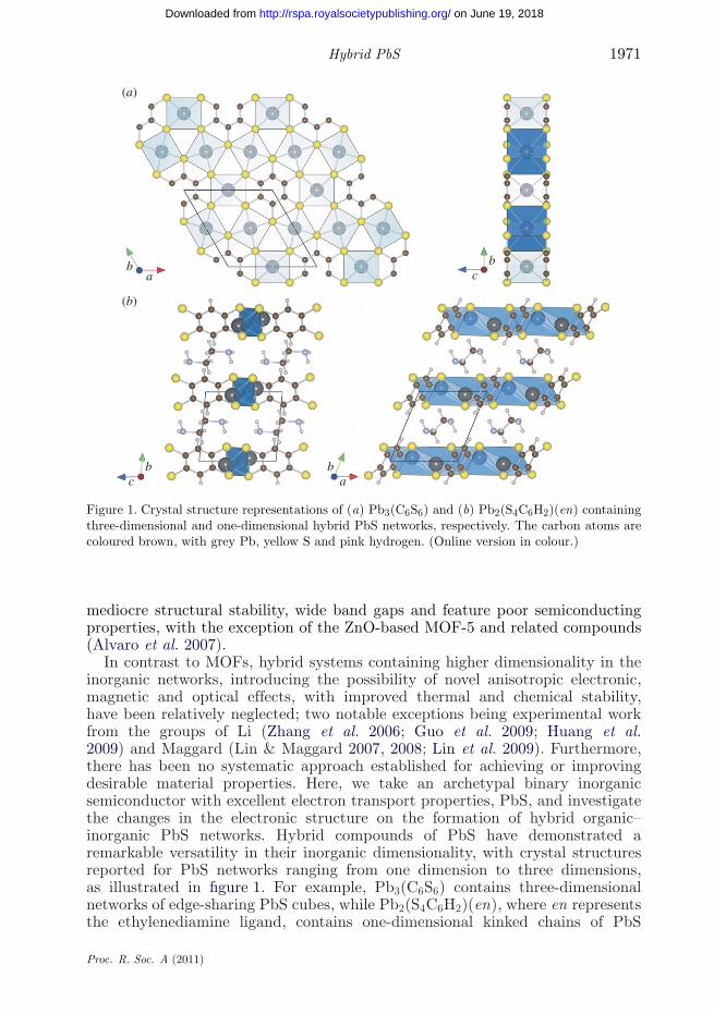
Figure 1. Crystal structure representations of (a) Pb3(C6S6) and (b) Pb2(S4C6H2)(en) containingthree-dimensional and one-dimensional hybrid PbS networks, respectively. The carbon atoms arecoloured brown, with grey Pb, yellow S and pink hydrogen. (Online version in colour.)
mediocre structural stability, wide band gaps and feature poor semiconductingproperties, with the exception of the ZnO-based MOF-5 and related compounds(Alvaro et al. 2007).
In contrast to MOFs, hybrid systems containing higher dimensionality in theinorganic networks, introducing the possibility of novel anisotropic electronic,magnetic and optical effects, with improved thermal and chemical stability,have been relatively neglected; two notable exceptions being experimental workfrom the groups of Li (Zhang et al. 2006; Guo et al. 2009; Huang et al.2009) and Maggard (Lin & Maggard 2007, 2008; Lin et al. 2009). Furthermore,there has been no systematic approach established for achieving or improvingdesirable material properties. Here, we take an archetypal binary inorganicsemiconductor with excellent electron transport properties, PbS, and investigatethe changes in the electronic structure on the formation of hybrid organic–inorganic PbS networks. Hybrid compounds of PbS have demonstrated aremarkable versatility in their inorganic dimensionality, with crystal structuresreported for PbS networks ranging from one dimension to three dimensions,as illustrated in figure 1. For example, Pb3(C6S6) contains three-dimensionalnetworks of edge-sharing PbS cubes, while Pb2(S4C6H2)(en), where en representsthe ethylenediamine ligand, contains one-dimensional kinked chains of PbS
Proc. R. Soc. A (2011)
on June 19, 2018http://rspa.royalsocietypublishing.org/Downloaded from
1972 A. Walsh
stacked along the triclinic a-axis. These two materials exhibit optical band gapsof 1.7 and 3.1 eV, respectively (Turner et al. 2008), covering the full rangeof the visible spectrum. This demonstrates the potential of hybrid materialsfor optoelectronic applications including photovoltaics and solid-state lighting,areas traditionally dominated by III–V, II–VI and related semiconductor alloys(Srivastava et al. 1985; Wei et al. 1990; Zhu et al. 2008; Chen et al. 2009b; Catlowet al. 2010).
In this work, we investigate changes in the electronic structure producedfrom the parent rocksalt-structured PbS on the formation of hybrid materialscontaining PbS polyhedra linked through three-dimensional and one-dimensionalnetworks with benzenehexathiol-derived organic ligands. Our calculations, basedon a first-principles density functional theory approach, highlight the effect ofquantum confinement in widening the intrinsic PbS band gap, in addition to themarked contributions of the organic components to the band-edge states and alsoto point defect formation. Finally, a design rationale for further engineering theelectronic properties of hybrid materials is proposed.
2. Computational methods
The electronic structure and total energy of rocksalt PbS and both hybrid PbSsystems were calculated using density functional theory (DFT; Hohenberg &Kohn 1964; Kohn & Sham 1965) within the code VASP (Kresse & Furthmüller1996a,b). Exchange-correlation effects were treated at the generalized gradientapproximation (GGA) level of theory, namely the Perdew–Burke Ernzerhof(PBE) functional (Perdew et al. 1996). A plane-wave basis set was employed,with the projector augmented wave method (Blöchl 1994) used to representthe valence–core (Pb:[Xe], C:[He], N:[He], S:[Ne]) interactions. Scalar-relativisticcontributions are explicitly included in the core potentials, while spin–orbitcoupling is not treated; previous calculations on PbS have shown that theinclusion of spin–orbit coupling lowers the degeneracy of the empty Pb 6p band,but does not significantly affect the valence band structure (Wei & Zunger1997). All calculations were performed on the HECToR supercomputer using, onaverage, 128 cores for a typical optimization job. The parallel efficiency of VASP(and similar plane-wave DFT codes) dramatically decreases for larger numbersof cores, primarily due to the increased cost (latency) of communication betweenthe computing nodes.
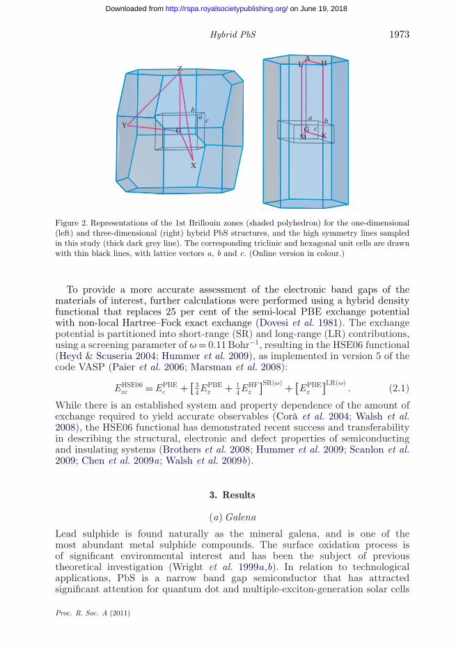
The plane-wave kinetic energy cut-off (500 eV) and the k-point sampling wereboth checked for convergence in both the total energies and equilibrium latticeconstants. The internal positions were relaxed using Quasi-Newton minimizationuntil the forces were below 0.005 eV Å−1. The equilibrium cell volumes wereobtained by performing a series of constant volume calculations and fitting theresulting energy–volume data to the Murnaghan equation of state (Murnaghan1944). The electronic band structures are plotted along high symmetry directionsof the respective first Brillouin zone of the primitive unit cells (Aroyo et al. 2006),which are illustrated for the two hybrid material structures in figure 2. The latticesite and angular momentum decomposed (local) electronic densities of states wereobtained by projecting the wavefunctions onto spherical harmonics centred ateach ion core.
Proc. R. Soc. A (2011)
on June 19, 2018http://rspa.royalsocietypublishing.org/Downloaded from
Hybrid PbS 1973
cab
Z
X
YG c
a b
AL
M K
H
G
Figure 2. Representations of the 1st Brillouin zones (shaded polyhedron) for the one-dimensional(left) and three-dimensional (right) hybrid PbS structures, and the high symmetry lines sampledin this study (thick dark grey line). The corresponding triclinic and hexagonal unit cells are drawnwith thin black lines, with lattice vectors a, b and c. (Online version in colour.)
To provide a more accurate assessment of the electronic band gaps of thematerials of interest, further calculations were performed using a hybrid densityfunctional that replaces 25 per cent of the semi-local PBE exchange potentialwith non-local Hartree–Fock exact exchange (Dovesi et al. 1981). The exchangepotential is partitioned into short-range (SR) and long-range (LR) contributions,using a screening parameter of u = 0.11 Bohr−1, resulting in the HSE06 functional(Heyd & Scuseria 2004; Hummer et al. 2009), as implemented in version 5 of thecode VASP (Paier et al. 2006; Marsman et al. 2008):
EHSE06xc = EPBE
c + [ 34E
PBEx + 1
4EHFx
]SR(u) + [EPBE
x
]LR(u). (2.1)
While there is an established system and property dependence of the amount ofexchange required to yield accurate observables (Corà et al. 2004; Walsh et al.2008), the HSE06 functional has demonstrated recent success and transferabilityin describing the structural, electronic and defect properties of semiconductingand insulating systems (Brothers et al. 2008; Hummer et al. 2009; Scanlon et al.2009; Chen et al. 2009a; Walsh et al. 2009b).
3. Results
(a) Galena
Lead sulphide is found naturally as the mineral galena, and is one of themost abundant metal sulphide compounds. The surface oxidation process isof significant environmental interest and has been the subject of previoustheoretical investigation (Wright et al. 1999a,b). In relation to technologicalapplications, PbS is a narrow band gap semiconductor that has attractedsignificant attention for quantum dot and multiple-exciton-generation solar cells
Proc. R. Soc. A (2011)
on June 19, 2018http://rspa.royalsocietypublishing.org/Downloaded from
1974 A. Walsh
–10
n (e
lect
rons
eV
–1)
ener
gy (
eV)
–8 –6
Pb s
bulk PbS
S p
S s
Pb p
–4 –2energy (eV)
0 2 4 6–10
–8
–6
–4
–2
0
2
4
6
L G X
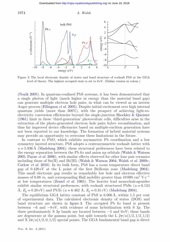
Figure 3. The local electronic density of states and band structure of rocksalt PbS at the GGAlevel of theory. The highest occupied state is set to 0 eV. (Online version in colour.)
(Nozik 2005). In quantum-confined PbS systems, it has been demonstrated thata single photon of light (much higher in energy than the material band gap)can generate multiple electron–hole pairs, in what can be viewed as an inverseAuger process (Ellingson et al. 2005). Despite initial excitement over high internalquantum yields (more than 300%), with the prospect of achieving light-to-electricity conversion efficiencies beyond the single-junction Shockley & Queisser(1961) limit in these ‘third-generation’ photovoltaic cells, difficulties arise in theextraction of the photo-generated electron–hole pairs before recombination, andthus far improved device efficiencies based on multiple-excition generation havenot been reported to our knowledge. The formation of hybrid material systemsmay provide an opportunity to overcome these limitations in the future.
In contrast to PbO, which exhibits asymmetric Pb coordination and a lowsymmetry layered structure, PbS adopts a centrosymmetric rocksalt lattice witha = 5.936 Å (Madelung 2004); these structural preferences have been related tothe energy separation between the Pb 6s and anion np orbitals (Walsh & Watson2005; Payne et al. 2006), with similar effects observed for other lone pair ceramicsincluding those of Sn(II) and Bi(III) (Walsh & Watson 2004; Walsh et al. 2009c;Catlow et al. 2010). In its bulk form, PbS has a room temperature direct bandgap of 0.420 eV at the L point of the first Brillouin zone (Madelung 2004).This small electronic gap results in remarkably low hole and electron effectivemasses of 0.08 me and corresponding Hall mobility greater than 10 000 cm2 V s−1
at low temperatures (Zemel et al. 1965). The heavier lead monochalcogenidesexhibit similar structural preferences, with rocksalt structured PbSe (a = 6.124Å, Eg = 0.28 eV) and PbTe (a = 6.462 Å, Eg = 0.31 eV) (Madelung 2004).
The equilibrium GGA lattice constant of PbS is 6.006 Å, within 1.5 per centof experimental data. The calculated electronic density of states (DOS) andband structure are shown in figure 3. The occupied Pb 6s band is presentbetween −6 and −8 eV, with evidence of some hybridization with S 3p. Thethree predominately S 3p bands are located between −5 and 0 eV; these bandsare degenerate at the gamma point, but split towards the L 2p/a(1/2, 1/2, 1/2)and X 2p/a(1/2, 0, 1/2) special points. The GGA fundamental band gap is direct
Proc. R. Soc. A (2011)
on June 19, 2018http://rspa.royalsocietypublishing.org/Downloaded from

Hybrid PbS 1975
Table 1. The equilibrium GGA structural and electronic parameters of the bulk and hybridPbS systems. The band gaps obtained from the hybrid HSE06 functional are also listed forcomparison. The corresponding experimental values (Madelung 2004; Turner et al. 2008) are shownin parenthesis. Note that the experimental band gaps were estimated from room temperature visiblelight absorption spectra for the hybrid materials.
bulk PbS three-dimensional hybrid one-dimensional hybrid
a (Å) 6.006 (5.936) 9.053 (8.964) 7.192 (6.938)b (Å) 7.356 (7.145)c (Å) 4.006 (3.958) 8.078 (7.891)a (◦) 90 90 85.60 (85.89)b (◦) 90 90 65.98 (66.56)g (◦) 90 120 68.07 (67.59)Pb–S (Å) 6 × 3.00 8 × 3.11 6 × 3.22EGGA
g (eV) 0.47 (0.42) 0.99 (1.7) 2.22 (3.1)
EHSE06g (eV) 0.84 (0.42) 1.84 (1.7) 3.15 (3.1)
at the L point (0.465 eV), with the conduction band composed predominatelyof Pb 6p states. The occurrence of the direct band gap away from the gammapoint has been explained by the hybridization between Pb 6s and S 3p, which issymmetry forbidden (Wei & Zunger 1997), i.e. in the rocksalt primitive unit cell,interatomic s bonding between s and p states are forbidden at the zone centre dueto their phase inequivalence (A1g and T2u representations, respectively). Similarrestrictions for the coupling of p and d states results in the indirect band gapof CdO (Mcguinness et al. 2003; Zhu et al. 2008). In comparison to experiment,the magnitude of the band gap for PbS is in good agreement; while this levelof theory typically underestimates the band gaps of insulating materials, for thecase of band gaps determined by anion and cation p orbitals, better agreementis generally found (Wei & Zunger 1997; Walsh & Watson 2005).
(b) Hybrid lead sulphide composites
Crystal structures for one-dimensional and three-dimensional hybrid organic–inorganic PbS composite networks have recently been determined (Turner et al.2008), which are illustrated in figure 1. The experimental structural parameters,measured at room temperature using powder X-ray diffraction, were taken as thestarting positions, which were then fully relaxed through DFT calculations, withthe resulting equilibrium structures and band gaps detailed in table 1.
The crystal structure of the three-dimensional hybrid system, Pb3(C6S6), ishexagonal (space group 191, P6/mmm) with one formula unit per repeating cell.The structure consists of alternating planes of Pb and S/C oriented along ofthe c-axis. Each Pb atom lies at the centre of a cube with eightfold sulphurcoordination, while each S atom is coordinated to four lead atoms and one carbonatom. The carbon atoms form sulphur-terminated planar hexagonal rings, i.e. aderivative of benzenehexathiol. The equilibrium GGA structural parameters arein good agreement with experiment, with errors of less than 1.5 per cent.
Proc. R. Soc. A (2011)
on June 19, 2018http://rspa.royalsocietypublishing.org/Downloaded from
1976 A. Walsh
–10
n (e
lect
rons
eV
–1)
ener
gy (
eV)
–8 –6
PbC
S
Pb s
–4 –2energy (eV)
0 2 4–1
0
1
2
A H K MG G L
Figure 4. The local electronic density of states and band structure of the three-dimensional PbShybrid material at the GGA level of theory. The highest occupied state is set to 0 eV. (Onlineversion in colour.)
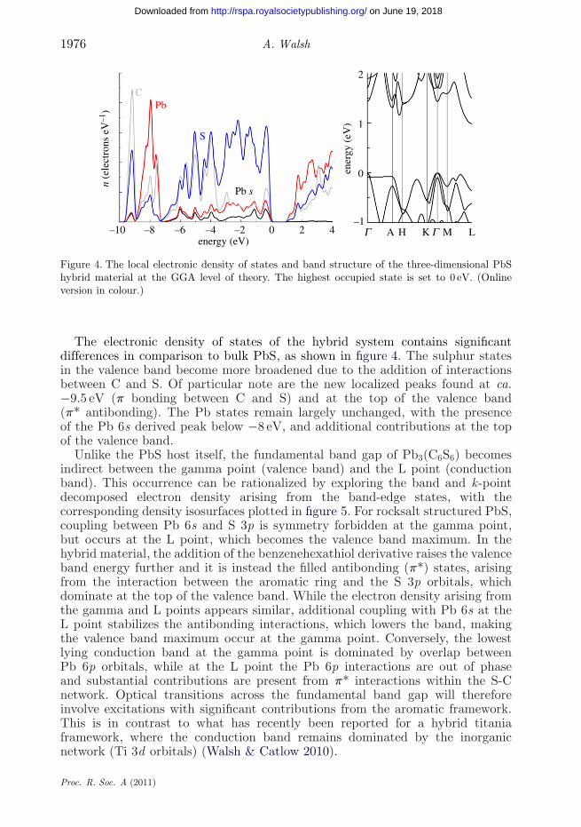
The electronic density of states of the hybrid system contains significantdifferences in comparison to bulk PbS, as shown in figure 4. The sulphur statesin the valence band become more broadened due to the addition of interactionsbetween C and S. Of particular note are the new localized peaks found at ca.−9.5 eV (p bonding between C and S) and at the top of the valence band(p* antibonding). The Pb states remain largely unchanged, with the presenceof the Pb 6s derived peak below −8 eV, and additional contributions at the topof the valence band.
Unlike the PbS host itself, the fundamental band gap of Pb3(C6S6) becomesindirect between the gamma point (valence band) and the L point (conductionband). This occurrence can be rationalized by exploring the band and k-pointdecomposed electron density arising from the band-edge states, with thecorresponding density isosurfaces plotted in figure 5. For rocksalt structured PbS,coupling between Pb 6s and S 3p is symmetry forbidden at the gamma point,but occurs at the L point, which becomes the valence band maximum. In thehybrid material, the addition of the benzenehexathiol derivative raises the valenceband energy further and it is instead the filled antibonding (p*) states, arisingfrom the interaction between the aromatic ring and the S 3p orbitals, whichdominate at the top of the valence band. While the electron density arising fromthe gamma and L points appears similar, additional coupling with Pb 6s at theL point stabilizes the antibonding interactions, which lowers the band, makingthe valence band maximum occur at the gamma point. Conversely, the lowestlying conduction band at the gamma point is dominated by overlap betweenPb 6p orbitals, while at the L point the Pb 6p interactions are out of phaseand substantial contributions are present from p* interactions within the S-Cnetwork. Optical transitions across the fundamental band gap will thereforeinvolve excitations with significant contributions from the aromatic framework.This is in contrast to what has recently been reported for a hybrid titaniaframework, where the conduction band remains dominated by the inorganicnetwork (Ti 3d orbitals) (Walsh & Catlow 2010).
Proc. R. Soc. A (2011)
on June 19, 2018http://rspa.royalsocietypublishing.org/Downloaded from
Hybrid PbS 1977
(a) (b)
(c) (d)
Figure 5. Electron density arising from the highest occupied band at the (a) G and (b) L pointsand the lowest unoccupied bands at the (c) G and (d) L points for the three-dimensional hybridmaterial. The carbon atoms are coloured brown, with grey Pb, yellow S and pink hydrogen. (Onlineversion in colour.)
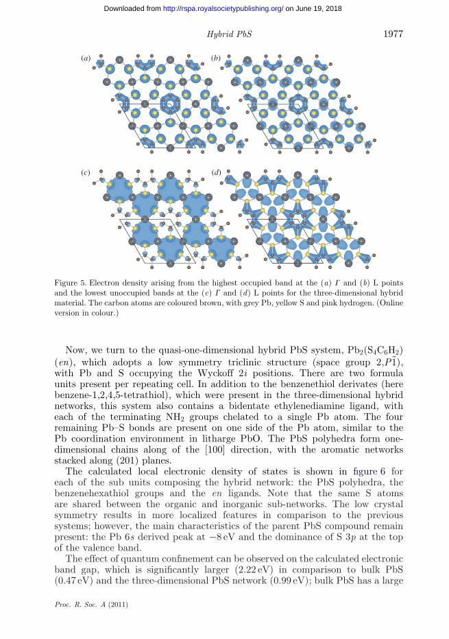
Now, we turn to the quasi-one-dimensional hybrid PbS system, Pb2(S4C6H2)(en), which adopts a low symmetry triclinic structure (space group 2,P 1̄),with Pb and S occupying the Wyckoff 2i positions. There are two formulaunits present per repeating cell. In addition to the benzenethiol derivates (herebenzene-1,2,4,5-tetrathiol), which were present in the three-dimensional hybridnetworks, this system also contains a bidentate ethylenediamine ligand, witheach of the terminating NH2 groups chelated to a single Pb atom. The fourremaining Pb–S bonds are present on one side of the Pb atom, similar to thePb coordination environment in litharge PbO. The PbS polyhedra form one-dimensional chains along of the [100] direction, with the aromatic networksstacked along (201) planes.
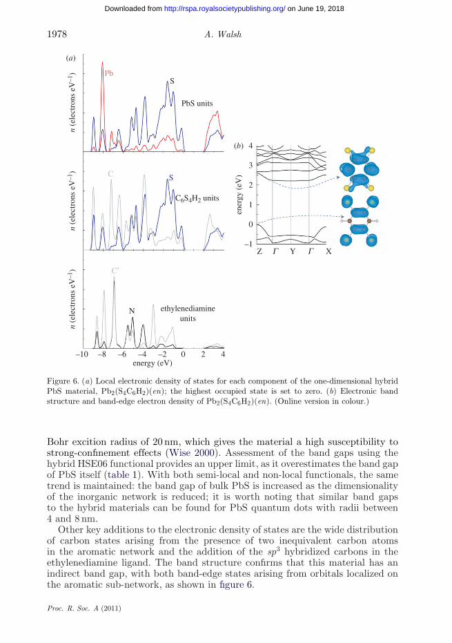
The calculated local electronic density of states is shown in figure 6 foreach of the sub units composing the hybrid network: the PbS polyhedra, thebenzenehexathiol groups and the en ligands. Note that the same S atomsare shared between the organic and inorganic sub-networks. The low crystalsymmetry results in more localized features in comparison to the previoussystems; however, the main characteristics of the parent PbS compound remainpresent: the Pb 6s derived peak at −8 eV and the dominance of S 3p at the topof the valence band.
The effect of quantum confinement can be observed on the calculated electronicband gap, which is significantly larger (2.22 eV) in comparison to bulk PbS(0.47 eV) and the three-dimensional PbS network (0.99 eV); bulk PbS has a large
Proc. R. Soc. A (2011)
on June 19, 2018http://rspa.royalsocietypublishing.org/Downloaded from
1978 A. Walsh
–10
n (e
lect
rons
eV
–1)
n (e
lect
rons
eV
–1)
n (e
lect
rons
eV
–1)
ener
gy (
eV)
–8 –6 –4 –2energy (eV)
0 2
ethylenediamineunits
C6S4H2 units
PbS units
S
(a)
(b)
S
Pb
N
C¢
C
4
Z–1
0
1
2
3
4
Y GG X
Figure 6. (a) Local electronic density of states for each component of the one-dimensional hybridPbS material, Pb2(S4C6H2)(en); the highest occupied state is set to zero. (b) Electronic bandstructure and band-edge electron density of Pb2(S4C6H2)(en). (Online version in colour.)
Bohr excition radius of 20 nm, which gives the material a high susceptibility tostrong-confinement effects (Wise 2000). Assessment of the band gaps using thehybrid HSE06 functional provides an upper limit, as it overestimates the band gapof PbS itself (table 1). With both semi-local and non-local functionals, the sametrend is maintained: the band gap of bulk PbS is increased as the dimensionalityof the inorganic network is reduced; it is worth noting that similar band gapsto the hybrid materials can be found for PbS quantum dots with radii between4 and 8 nm.
Other key additions to the electronic density of states are the wide distributionof carbon states arising from the presence of two inequivalent carbon atomsin the aromatic network and the addition of the sp3 hybridized carbons in theethylenediamine ligand. The band structure confirms that this material has anindirect band gap, with both band-edge states arising from orbitals localized onthe aromatic sub-network, as shown in figure 6.
Proc. R. Soc. A (2011)
on June 19, 2018http://rspa.royalsocietypublishing.org/Downloaded from

Hybrid PbS 1979
valence band
0.01
0.120.15VSVx
SVx
Pb 0.03VPb
0.78
1.31
0.47
0.99
0.04 0.05VxS
galena hybrid PbS
conduction band
VxPb VPb
VS
Figure 7. Schematic of the adiabatic defect ionization levels within the band gap of the bulk andhybrid PbS systems calculated using density functional theory at the GGA level. (Online versionin colour.)
Table 2. Point defect reaction energies.
defect reaction bulk PbS three-dimensional hybrid
SS � V×S + S(s) 1.77 2.47
PbPb � V×Pb + Pb(s) 1.36 1.74
PbPb + SS � V×Pb + V×
S + PbS(s) 1.04 1.58PbPb + SS � V/
Pb + V•S + PbS(s) 0.87 1.43
PbPb + SS � V//
Pb + V••S + PbS(s) 0.69 1.55
For the hybrid material, the Schottky reaction is balanced through the precipitation of bulk PbS.All values are in eV per defect.
(c) Defect chemistry
Analysis of the intrinsic defect reactions in the bulk and three-dimensionalhybrid PbS systems, the details of which have been presented elsewhere (Walsh2010), have indicated a particularly low formation energy and shallow ionizationlevels for cation vacancies, which would suggest that the hybrid materials willfavour intrinsic p-type behaviour. The defect reaction energies are listed intable 2, with the thermal ionization levels shown in figure 7. As the top of thevalence band is composed of antibonding interactions between S 3p and Pb 6sin PbS (Walsh & Watson 2005), emptying these states is accompanied by onlya small energetic penalty, similar to the antibonding O 2p/Cu 3d states in thep-type oxide semiconductor Cu2O (Nolan & Elliott 2006; Scanlon et al. 2009; Soonet al. 2009). The same orbital character is observed in the high-energy bands ofthe three-dimensional hybrid material with the addition of delocalized p* states.
In contrast to the lead vacancy, the sulphur vacancy in PbS results in a deepdefect level, predominately localized in the vacancy site, i.e. an F-centre (or colourcentre), which may be viewed as a two-electron He analogous to the hydrogenicone-electron F-centre observed in alkali halides (Stoneham 1975). In this case,
Proc. R. Soc. A (2011)
on June 19, 2018http://rspa.royalsocietypublishing.org/Downloaded from

1980 A. Walsh
0.02 Å 0.10 Å 0.15 Å
179.11°(a) (b) (c)176.56° 174.48°
Figure 8. Equilibrium geometries around (a) V×S , (b) V•
S and (c) V••S in galena. The S–Pb–S bond
angles and Pb displacements, shown relative to the ideal bulk positions, are isotropic around thedefect site. (Online version in colour.)
the F-centre is accompanied by significant polarization of the neighbouring Pbsites. In the hybrid material, the defect charge density is again associated witha localized centre, but there is additional hybridization with the neighbouring pframework: see Walsh (2010).
Ionization of the localized anion vacancy centres shows different behaviour inthe bulk and hybrid systems: the F+ centre is thermodynamically unstable inPbS, exhibiting negative U behaviour, where U represents the on-site repulsiveCoulomb interaction between two electrons (Anderson 1975; Yu & Cardona 2005).In such a case, negative U refers to the situation where the second electron isattracted to the defect state, and a direct transition is observed between the closedshell neutral and doubly ionized point defect centres. In other words, in thermalequilibrium, the F+ centre will only be metastable: for any equilibrium position ofthe Fermi energy within the band gap, the defect state will exist either as an F orF++ centre. Ionization of V×
S in galena results in an isotropic outward expansionof the neighbouring Pb ions as shown in figure 8. In the hybrid material, similarionic relaxation occurs but the V•
S centre is further stabilized electronically dueto interaction with the organic sub-lattice, and the V•→••
S transition lies resonantwithin the valence band. If produced in sufficient quantities, the paramagneticV•
S centre should be observable through spectroscopic methods, such as electronspin resonance.
The energies for Schottky pair formation (intrinsic ionic disorder involving non-interacting site vacancies) are listed in table 2. Both materials exhibit a preferencefor charged Schottky formation owing to the beneficial electron transfer betweendonor and acceptor states; however, the charge state preferences differ in thetwo cases: PbS favours doubly charged (fully ionized) disorder, while Pb3(C6S6)favours the single ionized Schottky disorder as the defect level of V••
S lies belowthat of V//
Pb. The Schottky energies, ranging from 0.7 to 1.6 eV per defect, aremuch smaller than those observed in wide band gap metal oxide and III–Vsystems, e.g. 4.44 eV in In2O3 (Walsh et al. 2009a), 3.45 eV in ZnO (Sokol et al.2007; Catlow et al. 2008), 3.67 eV in SnO2 (Godinho et al. 2009), and 4.7 eVin GaN (Catlow et al. 2010). For all defect reactions, the formation energies
Proc. R. Soc. A (2011)
on June 19, 2018http://rspa.royalsocietypublishing.org/Downloaded from
Hybrid PbS 1981
are substantially higher in the hybrid materials, which would suggest that theirconcentrations will be much lower: to produce semiconducting samples, it maybe necessary to extrinsically dope these materials.
4. Discussion
A number of key changes have been observed in the transition from bulk PbSto the quasi-one-dimensional hybrid PbS material. Bulk PbS is a direct bandgap, low effective mass semiconductor. On transition to the three-dimensionalhybrid network, the local PbS bonding network is perturbed and the valenceand conduction band-edge states contain contributions from hybridized statesof both the organic and inorganic sub-networks. However, while the band gapis opened, significant band dispersion is maintained, which should contribute toreasonable carrier mobility in the hybrid materials. Unfortunately, indirect bandgaps are predicted, which could limit radiative recombination of electrons andholes for light-emission applications. Investigation of the primary defect reactionssuggests that a number of parallels exist between the bulk and hybrid systems;most importantly, Pb vacancies exist as low energy shallow electron acceptingdefects in both cases, while sulphur vacancies exist as deep colour centres. In allmaterials studied, the contribution of the organic ligands to the band-edge statesis appreciable, and the resulting electron transport properties will therefore relyon the cooperative behaviour between the inorganic and organic networks.
Three avenues for chemical functionalization can be envisioned in hybridmaterials, which extend beyond the prototype PbS compounds studied here:
— In terms of the aromatic ligands, incorporation of acidic or basic functionalgroups could be used to engineer the band-edge positions (adjustingthe effective ionization potentials and electron affinities), which in turnwill affect both the visible light absorption and defect properties. Directexamples would include the substitution of electron withdrawing groupssuch as an alcohol, amine or triflouromethyl compounds into the aromaticring, or the addition of electron donating groups such as a methyl oraldehyde derivative.
— In terms of the inorganic network, similar frameworks could be built, whilemaintaining the underlying II–VI framework, for example, the replacementof Pb with alternative divalent cationic species such as Sn, Cd or Zn.Partial substitutions to form hybrid II–VI alloys, e.g. (Zn,Sn)S materials,may also be feasible considering the mechanical flexibility of the organicnetwork to compensate for alloy strain. Alternatively, cation mutationcould be performed producing multi-ternary semiconductors analogousto chalcopyrite (e.g. CuGaSe2) and kesterite (e.g. CuZnSnS4) solar cellabsorbers (Goodman 1958; Chen et al. 2009a,b, 2010).
— Isoelectronic modification of the anions is also feasible, forming thecorresponding oxides, selenides or tellurides. In most cases, oxideformation would be expected to increase the band gap, through theaddition of more localized, higher binding energy, O 2p orbitals andenhanced electron transfer. Conversely, the addition of Te would beexpected to decrease the band gap. Forming intermediate systems of
Proc. R. Soc. A (2011)
on June 19, 2018http://rspa.royalsocietypublishing.org/Downloaded from
1982 A. Walsh
mixed composition, e.g. oxysulphide hybrid compounds, would introducean extra degree of freedom, as demonstrated by the purely inorganicoxysulphide class of p-type transparent oxide semiconductors (Ueda et al.2000; Scanlon & Watson 2009).
A computational exploration of these design principles is currently in progress.
5. Conclusions
Using first-principles electronic structure calculations, we have investigated thechanges in electronic structure and chemical bonding on transition from bulk PbSto hybrid organic–inorganic networks containing three and one dimensionalitiesin the PbS interactions. In particular, our analysis highlighted:
— The contributions of the aromatic subnetworks to the band-edge statesactive in electron transport.
— A large increase in electronic band gap on formation of the hybridcompounds comparable to PbS quantum dots with radii of 4 to 8 nm.
— Comparable defect chemistry between the hybrid and inorganic parentPbS systems.
— Accessible routes for chemical engineering of the electronic properties ofhybrid materials.
The results emphasize the potential of hybrid materials as functionalsemiconducting materials, an area that is presently growing, and can resultin viable new directions for obtaining materials chemically engineered forphotovoltaic and optoelectronic devices. The role of materials simulation inproviding predictive guidance can help to rapidly progress research in this area.
I would like to acknowledge stimulating discussions with T. P. Vaid, A. K. Cheetham,C. R. A. Catlow, A. A. Sokol, S. M. Woodley and D. Demathieu. This work was funded througha Marie-Curie Intra-European Fellowship on ‘Electronic Structure Modelling of Hybrid Organic-Inorganic Semiconductors’ from the European Union under the Seventh Framework Programme.Via my membership of the UK’s HPC Materials Chemistry Consortium, which is funded by EPSRC(EP/F067496), this work made use of the facilities of HECToR, the UK’s national high-performancecomputing service. I also acknowledge use of the UCL Legion High Performance Computing Facility,and associated support services, in the completion of this work.
References
Alvaro, M., Carbonell, E., Belén, F., Llabrés, I., Xamena, F. X. & Hermenegildo, G. 2007Semiconductor behavior of a metal–organic framework (MOF). Chem. Eur. J. 13, 5106–5112.(doi:10.1002/chem.200601003)
Anderson, P. W. 1975 Model for the electronic structure of amorphous semiconductors. Phys. Rev.Lett. 34, 953–955. (doi:10.1103/PhysRevLett.34.953)
Aroyo, M. I., Kirov, A., Capillas, C., Perez-Mato, J. M. & Wondratschek, H. 2006 Bilbaocrystallographic server. II. Representations of crystallographic point groups and space groups.Acta Crystallogr. Sect. A 62, 115–128. (doi:10.1107/S0108767305040286)
Proc. R. Soc. A (2011)
on June 19, 2018http://rspa.royalsocietypublishing.org/Downloaded from
Hybrid PbS 1983
Blöchl, P. E. 1994 Projector augmented-wave method. Phys. Rev. B 50, 17 953–17 979.(doi:10.1103/PhysRevB.50.17953)
Brothers, E. N., Izmaylov, A. F., Normand, J. O., Barone, V. & Scuseria, G. E. 2008 Accuratesolid-state band gaps via screened hybrid electronic structure calculations. J. Chem. Phys. 129,011102. (doi:10.1063/1.2955460)
Catlow, C. R. A., French, S. A., Sokol, A. A., Al-Sunaidi, A. A. & Woodley, S. M. 2008 Zincoxide: a case study in contemporary computational solid state chemistry. J. Comput. Chem. 29,2234–2249. (doi:10.1002/jcc.21051)
Catlow, C. R. A., Guo, Z. X., Miskufova, M., Shevlin, S. A., Smith, A. G. H., Sokol, A. A.,Walsh, A., Wilson, D. J. & Woodley, S. M. 2010 Advances in computational studies of energymaterials. Phil. Trans. R. Soc. A 368, 3379–3456. (doi:10.1098/rsta.2010.0111)
Cheetham, A. K. & Rao, C. N. R. 2007 Materials science: there’s room in the middle. Science 318,58–59. (doi:10.1126/science.1147231)
Cheetham, A. K., Rao, C. N. R. & Feller, R. K. 2006 Structural diversity and chemical trendsin hybrid inorganic–organic framework materials. Chem. Comm. 46, 4780–4795. (doi:10.1039/b610264f)
Chen, S., Gong, X. G., Walsh, A. & Wei, S.-H. 2009a Crystal and electronic band structure ofCu2ZnSnX4 (X = S and Se) photovoltaic absorbers: first-principles insights. Appl. Phys. Lett.94, 041903. (doi:10.1063/1.3074499)
Chen, S., Gong, X. G., Walsh, A. & Wei, S.-H. 2009b Electronic structure and stability ofquaternary chalcogenide semiconductors derived from cation cross-substitution of II–VI andI–III–VI2 compounds. Phys. Rev. B 79, 165211. (doi:10.1103/PhysRevB.79.165211)
Chen, S., Gong, X. G., Walsh, A. & Wei, S.-H. 2010 Defect physics of the kesterite thin-film solarcell absorber Cu2ZnSnS4. Appl. Phys. Lett. 96, 021902. (doi:10.1063/1.3275796)
Corà, F., Alfredsson, M., Mallia, G., Middlemiss, D. S., Mackrodt, W. C., Dovesi, R. & Orlando, R.2004 The performance of hybrid density functionals in solid state chemistry. Chem. Mater. Sci.113, 171–232. (doi:10.1007/b97944)
Dovesi, R., Causà, M. & Angonoa, G. 1981 Exact-exchange Hartree–Fock calculations for periodicsystems. V. Ground-state properties of silicon. Phys. Rev. B 24, 4177–4183. (doi:10.1103/PhysRevB.24.4177)
Ellingson, R. J., Beard, M. C., Johnson, J. C., Yu, P., Micic, O. I., Nozik, A. J., Shabaev, A. &Efros, A. L. 2005 Highly efficient multiple exciton generation in colloidal PbSe and PbS quantumdots. Nano Lett. 5, 865–871. (doi:10.1021/nl0502672)
Ferey, G. 2001 Microporous solids: from organically templated inorganic skeletons to hybridframeworks—ecumenism in chemistry. Chem. Mater. 13, 3084–3098. (doi:10.1021/cm011070n)
Godinho, K. G., Walsh, A. & Watson, G. W. 2009 Energetic and electronic structure analysis ofintrinsic defects in SnO2. J. Phys. Chem. C 113, 439–448. (doi:10.1021/jp807753t)
Goodman, C. H. L. 1958 The prediction of semiconducting properties in inorganic compounds.J. Phys. Chem. Solids 6, 305–314. (doi:10.1016/0022-3697(58)90050-7)
Guo, Z., Cao, R., Wang, X., Li, H., Yuan, W., Wang, G., Wu, H. & Li, J. 2009 A Multifunctional3D ferroelectric and NLO-active porous metal-organic framework. J. Am. Chem. Soc. 131, 6894–6895. (doi:10.1021/ja9000129)
Heyd, J. & Scuseria, G. E. 2004 Efficient hybrid density functional calculations in solids: assessmentof the Heyd–Scuseria–Ernzerhof screened Coulomb hybrid functional. J. Chem. Phys. 121,1187–1192. (doi:10.1063/1.1760074)
Hohenberg, P. & Kohn, W. 1964 Inhomogeneous electron gas. Phys. Rev. 136, B864–B871.(doi:10.1103/PhysRev.136.B864)
Huang, X., Roushan, M., Emge, T. J., Bi, W., Thiagarajan, S., Cheng, J.-H., Yang, R. & Li, J.2009 Flexible hybrid semiconductors with low thermal conductivity: the role of organic diamines.Angew. Chem. Int. Ed. 48, 7871–7874. (doi:10.1002/anie.200903234)
Hummer, K., Harl, J. & Kresse, G. 2009 Heyd–Scuseria–Ernzerhof hybrid functional forcalculating the lattice dynamics of semiconductors. Phys. Rev. B 80, 115205. (doi:10.1103/PhysRevB.80.115205)
Kohn, W. & Sham, L. J. 1965 Self-consistent equations including exchange and correlation effects.Phys. Rev. 140, A1133–A1138. (doi:10.1103/PhysRev.140.A1133)
Proc. R. Soc. A (2011)
on June 19, 2018http://rspa.royalsocietypublishing.org/Downloaded from
1984 A. Walsh
Kresse, G. & Furthmüller, J. 1996a Efficiency of ab initio total energy calculations for metalsand semiconductors using a plane-wave basis set. Comput. Mater. Sci. 6, 15–50. (doi:10.1016/0927-0256(96)00008-0)
Kresse, G. & Furthmüller, J. 1996b Efficient iterative schemes for ab initio total-energy calculationsusing a plane-wave basis set. Phys. Rev. B 54, 11 169–11 186. (doi:10.1103/PhysRevB.54.11169)
Lin, H. & Maggard, P. A. 2007 Copper(I)-rhenate hybrids: syntheses, structures, and opticalproperties. Inorg. Chem. 46, 1283. (doi:10.1021/ic061767g)
Lin, H. S. & Maggard, P. A. 2008 Synthesis and structures of a new series of silver–vanadatehybrid solids and their optical and photocatalytic properties. Inorg. Chem. 47, 8044–8052.(doi:10.1021/ic8004129)
Lin, H. S., Wu, X. M. & Maggard, P. A. 2009 Ligand-based modification of the structures andoptical properties of new silver(i)-rhenate(vii) oxide/organic hybrid solids. Inorg. Chem. 48,11 265–11 276. (doi:10.1021/ic901749r)
Madelung, O. M. 2004 Semiconductors: data handbook. Berlin, Germany: Springer.Marsman, M., Paier, J., Stroppa, A. & Kresse, G. 2008 Hybrid functionals applied to extended
systems. J. Phys. Condensed Matter 20, 064201. (doi:10.1088/0953-8984/20/6/064201)McGuinness, C., Stagarescu, C. B., Ryan, P. J., Downes, J. E., Fu, D., Smith, K. E. & Egdell,
R. G. 2003 Influence of shallow core-level hybridization on the electronic structure of post-transition-metal oxides studied using soft X-ray emission and absorption. Phys. Rev. B 68,165104. (doi:10.1103/PhysRevB.68.165104)
Mellot-Draznieks, C. 2007 Role of computer simulations in structure prediction and structuredetermination: from molecular compounds to hybrid frameworks. J. Mater. Chem. 17,4348–4358. (doi:10.1039/b702516p)
Murnaghan, F. D. 1944 The compressibility of media under extreme pressures. Proc. Natl Acad.Sci. USA 30, 244–247. (doi:10.1073/pnas.30.9.244)
Nolan, M. & Elliott, S. D. 2006 The p-type conduction mechanism in Cu2O: a first principles study.Phys. Chem. Chem. Phys. 8, 5350–5358. (doi:10.1039/b611969g)
Nozik, A. J. 2005 Exciton multiplication and relaxation dynamics in quantum dots:applications to ultrahigh-efficiency solar photon conversion. Inorg. Chem. 44, 6893–6899.(doi:10.1021/ic0508425)
Paier, J., Marsman, M., Hummer, K., Kresse, G., Gerber, I. C. & Angyan, J. G. 2006Screened hybrid density functionals applied to solids. J. Chem. Phys. 124, 154709.(doi:10.1063/1.2187006)
Payne, D. J., Egdell, R. G., Walsh, A., Watson, G. W., Guo, J., Glans, P. A., Learmonth, T. &Smith, K. E. 2006 Electronic origins of structural distortions in post-transition metal oxides:experimental and theoretical evidence for a revision of the lone pair model. Phys. Rev. Lett. 96,157403. (doi:10.1103/PhysRevLett.96.157403)
Perdew, J. P., Burke, K. & Ernzerhof, M. 1996 Generalized gradient approximation made simple.Phys. Rev. Lett. 77, 3865–3868. (doi:10.1103/PhysRevLett.77.3865)
Rao, C. N. R., Cheetham, A. K. & Thirumurugan, A. 2008 Hybrid inorganic–organic materials: anew family in condensed matter physics. J. Phys.: Condensed Matter 20, 083202. (doi:10.1088/0953-8984/20/8/083202)
Scanlon, D. O. & Watson, G. W. 2009 (Cu2S2)(Sr3Sc2O5)–a layered, direct band gap, p-typetransparent conducting oxychalcogenide: a theoretical analysis. Chem. Mater. 21, 5435–5442.(doi:10.1021/cm902260b)
Scanlon, D. O., Morgan, B. J., Watson, G. W. & Walsh, A. 2009 Acceptor levels in p-type Cu2O:rationalizing theory and experiment. Phys. Rev. Lett. 103, 096405. (doi:10.1103/PhysRevLett.103.096405)
Shockley, W. & Queisser, H. J. 1961 Detailed balance limit of efficiency of p–n junction solar cells.J. Appl. Phys. 32, 510. (doi:10.1063/1.1736034)
Sokol, A. A., French, S. A., Bromley, S. T., Catlow, C. R. A., Dam, H. J. J. V. & Sherwood, P.2007 Point defects in ZnO. Faraday Discussions 134, 267–282. (doi:10.1039/b607406e)
Soon, A., Cui, X.-Y., Delley, B., Wei, S.-H. & Stampfl, C. 2009 Native defect-induced multifariousmagnetism in nonstoichiometric cuprous oxide: first-principles study of bulk and surfaceproperties of Cu2O. Phys. Rev. B 79, 035205. (doi:10.1103/PhysRevB.79.035205)
Proc. R. Soc. A (2011)
on June 19, 2018http://rspa.royalsocietypublishing.org/Downloaded from

Hybrid PbS 1985
Srivastava, G. P., Martins, J. L. & Zunger, A. 1985 Atomic structure and ordering in semiconductoralloys. Phys. Rev. B 31, 2561–2564. (doi:10.1103/PhysRevB.31.2561)
Stoneham, A. M. 1975 Theory of defects in solids. New York, NY: Oxford University Press.Turner, D. L., Vaid, T. P., Stephens, P. W., Stone, K. H., Dipasquale, A. G. & Rheingold, A.
L. 2008 Semiconducting lead–sulfur-organic network solids. J. Am. Chem. Soc. 130, 14–15.(doi:10.1021/ja0770983)
Ueda, K., Inoue, S., Hirose, S., Kawazoe, H. & Hosono, H. 2000 Transparent p-type semiconductor:LaCuOS layered oxysulfide. Appl. Phys. Lett. 77, 2701–2703. (doi:10.1063/1.1319507)
Walsh, A. 2010 Defect processes in a PbS metal organic framework: a quantum-confined hybridsemiconductor. J. Phys. Chem. Lett. 1, 1284–1287. (doi:10.1021/jz100312y)
Walsh, A. & Catlow, C. R. A. 2010 Photostimulated reduction processes in a titania hybrid metal–organic framework. Chem. Phys. Chem. 11, 2341–2344. (doi:10.1002/cphc.201000306)
Walsh, A. & Watson, G. W. 2004 Electronic structures of rocksalt, litharge, and herzenbergite SnOby density functional theory. Phys. Rev. B 70, 235114. (doi:10.1103/PhysRevB.70.235114)
Walsh, A. & Watson, G. W. 2005 The origin of the stereochemically active Pb(II) lone pair:DFT calculations on PbO and PbS. J. Solid State Chem. 178, 1422–1428. (doi:10.1016/j.jssc.2005.01.030)
Walsh, A., Da Silva, J. L. F. & Wei, S.-H. 2008 Theoretical description of magnetism in cobaltdoped ZnO. Phys. Rev. Lett. 100, 256401.
Walsh, A., Catlow, C. R. A., Sokol, A. A. & Woodley, S. M. 2009a Physical properties, Intrinsicdefects, and phase stability of indium sesquioxide. Chem. Mater. 21, 4962–4969. (doi:10.1021/cm902280z)
Walsh, A., Da Silva, J. L. F., Yan, Y., Al-Jassim, M. M. & Wei, S.-H. 2009b Origin of electronic andoptical trends in ternary In2O3(ZnO)n transparent conducting oxides (n = 1,3,5): Hybrid densityfunctional theory calculations. Phys. Rev. B 79, 073105. (doi:10.1103/PhysRevB.79.073105)
Walsh, A., Yan, Y., Huda, M. N., Al-Jassim, M. M. & Wei, S.-H. 2009c Band edge electronicstructure of BiVO4: elucidating the role of the Bi s and V d orbitals. Chem. Mater. 21, 547–551.(doi:10.1021/cm802894z)
Wei, S.-H. & Zunger, A. 1997 Electronic and structural anomalies in lead chalcogenides. Phys. Rev.B 55, 13605. (doi:10.1103/PhysRevB.55.13605)
Wei, S.-H., Ferreira, L. G., Bernard, J. E. & Zunger, A. 1990 Electronic properties of random alloys:special quasirandom structures. Phys. Rev. B 42, 9622–9649. (doi:10.1103/PhysRevB.42.9622)
Wise, F. W. 2000 Lead salt quantum dots: the limit of strong quantum confinement. AccountsChem. Res. 33, 773–780. (doi:10.1021/ar970220q)
Wright, K., Hillier, I. H., Vaughan, D. J. & Vincent, M. A. 1999a Cluster models of the dissociationof water on the surface of galena (PbS). Chem. Phys. Lett. 299, 527–531. (doi:10.1016/S0009-2614(98)01312-8)
Wright, K., Hillier, I. H., Vincent, M. A. & Kresse, G. 1999b Dissociation of water on the surfaceof galena (PbS): a comparison of periodic and cluster models. J. Chem. Phys. 111, 6942–6946.(doi:10.1063/1.479986)
Yu, P. Y. & Cardona, M. 2005 Fundamentals of semiconductors. Berlin, Germany: Springer.Zemel, J. N., Jensen, J. D. & Schoolar, R. B. 1965 Electrical and optical properties of epitaxial films
of PbS, PbSe, PbTe, and SnTe. Phys. Rev. 140, A330–A342. (doi:10.1103/PhysRev.140.A330)Zhang, Y., Dalpian, G. M., Fluegel, B., Wei, S.-H., Mascarenhas, A., Huang, X. Y., Li, J. &
Wang, L. W. 2006 Novel approach to tuning the physical properties of organic–inorganic hybridsemiconductors. Phys. Rev. Lett. 96, 026405. (doi:10.1103/PhysRevLett.96.026405)
Zhu, Y. Z., Chen, G. D., Ye, H. G., Walsh, A., Moon, C. Y. & Wei, S.-H. 2008 Electronic structureand phase stability of MgO, ZnO, CdO, and related ternary alloys. Phys. Rev. B 77, 245209.(doi:10.1103/PhysRevB.77.245209)
Proc. R. Soc. A (2011)
on June 19, 2018http://rspa.royalsocietypublishing.org/Downloaded from