Effects of High Frequency Voltage Stress on Air Insulation and Solid Insulation€¦ · ·...
18
Effects of High Frequency Voltage Stress on Air Insulation and Solid Insulation
-
Upload
phungkhuong -
Category
Documents
-
view
214 -
download
1
Transcript of Effects of High Frequency Voltage Stress on Air Insulation and Solid Insulation€¦ · ·...

Effects of High Frequency Voltage Stress on Air Insulation and Solid Insulation

Effects of High Frequency Voltage Stress on Air Insulation and Solid Insulation
page 2
Abstract — Air insulation and solid insulation are the most common approaches used to achieve adequate electrical insulation. However, with the increase in instances of high- frequency voltage stress, there are important differences in dimensioning these product safety approaches. This paper discusses the phenomenon of partial discharge and its impact on the behavior of clearances, creepage distances and solid insulation. To shorten the learning curve for a new procedure for determining clearances, a flowchart developed to identify the key distinguishing factors to be considered is also presented. Finally, the paper provides a case study of an investigation of a novel switch mode power supply.
Presented at the 2010 IEEE Product Safety Engineering Symposium
IntroductionAchieving safe voltages in electrical and electronic equipment depends on more than just using a step-down converter or a transformer, but on the variety of electrical insulation protection schemes incorporated into the device as well. Even the smallest breakdown in electrical insulation can make parts and circuits accessible to users unsafe, creating the potential for an electric shock that is capable of causing pain or injury. That’s why determining the shortest required distance to provide adequate insulation between two electrodes is a routine exercise for product safety engineers. For some time, the insulation requirements
for frequencies up to 30 kHz have been routinely applied to insulation stressed by voltages operating at frequencies greater than 30 kHz. Yet, the deteriorating effect of a partial discharge is increased roughly in proportion to the increased frequency. Therefore, with the introduction of high- frequency voltage stress considerations in IEC 62368-1:2010, the product safety standard for audio/video, information and communication technology equipment, it is important to understand the differences in the application of high frequency requirements, and how clearances, creepage distances and solid insulation can reduce the likelihood of insulation breakdown.
Effects of High Frequency Voltage Stress on Air Insulation and Solid Insulation
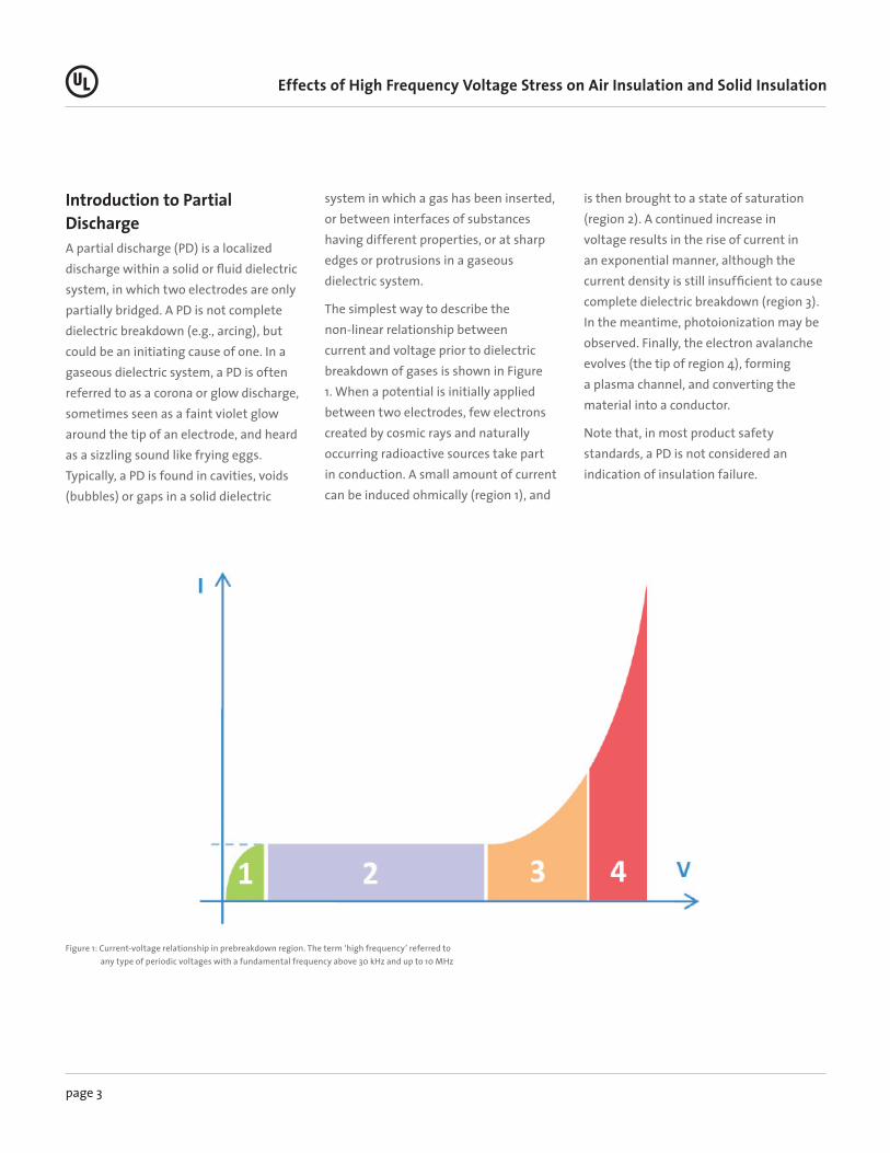
Figure 1: Current-voltage relationship in prebreakdown region. The term ‘high frequency’ referred to any type of periodic voltages with a fundamental frequency above 30 kHz and up to 10 MHz
Effects of High Frequency Voltage Stress on Air Insulation and Solid Insulation
page 3
Introduction to Partial DischargeA partial discharge (PD) is a localized discharge within a solid or fluid dielectric system, in which two electrodes are only partially bridged. A PD is not complete dielectric breakdown (e.g., arcing), but could be an initiating cause of one. In a gaseous dielectric system, a PD is often referred to as a corona or glow discharge, sometimes seen as a faint violet glow around the tip of an electrode, and heard as a sizzling sound like frying eggs. Typically, a PD is found in cavities, voids (bubbles) or gaps in a solid dielectric
system in which a gas has been inserted, or between interfaces of substances having different properties, or at sharp edges or protrusions in a gaseous dielectric system.
The simplest way to describe the non-linear relationship between current and voltage prior to dielectric breakdown of gases is shown in Figure 1. When a potential is initially applied between two electrodes, few electrons created by cosmic rays and naturally occurring radioactive sources take part in conduction. A small amount of current can be induced ohmically (region 1), and
is then brought to a state of saturation (region 2). A continued increase in voltage results in the rise of current in an exponential manner, although the current density is still insufficient to cause complete dielectric breakdown (region 3). In the meantime, photoionization may be observed. Finally, the electron avalanche evolves (the tip of region 4), forming a plasma channel, and converting the material into a conductor.
Note that, in most product safety standards, a PD is not considered an indication of insulation failure.
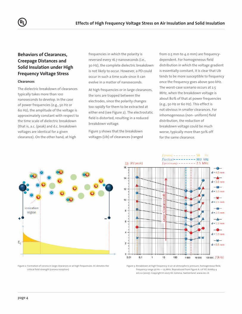
Figure 2: Formation of corona in large clearances or at high frequencies. EC denotes the critical field strength (corona inception)
Figure 3: Breakdown at high frequency in air at atmospheric pressure, homogeneous field, frequency range 50 Hz — 25 MHz. Reproduced from Figure A.1 of IEC 60664-4 ed.2.0 (2005). Copyright © 2005 IEC Geneva, Switzerland. www.iec.ch
Effects of High Frequency Voltage Stress on Air Insulation and Solid Insulation
page 4
Behaviors of Clearances, Creepage Distances and Solid Insulation under High Frequency Voltage StressClearances
The dielectric breakdown of clearances typically takes more than 100 nanoseconds to develop. In the case of power frequencies (e.g., 50 Hz or 60 Hz), the amplitude of the voltage is approximately constant with respect to the time scale of dielectric breakdown (that is, a.c. (peak) and d.c. breakdown voltages are identical for a given clearance). On the other hand, at high
frequencies in which the polarity is reversed every 16.7 nanoseconds (i.e., 30 Hz), the complete dielectric breakdown is not likely to occur. However, a PD could occur in such a time scale since it can evolve in a matter of nanoseconds.
At high frequencies or in large clearances, the ions are trapped between the electrodes, since the polarity changes too rapidly for them to be extracted at either end (see Figure 2). The electrostatic field is distorted, resulting in a reduced breakdown voltage.
Figure 3 shows that the breakdown voltages (Ub) of clearances (ranged
from 0.5 mm to 4.0 mm) are frequency-dependent. For homogeneous field distribution in which the voltage gradient is essentially constant, it is clear that Ub tends to be more susceptible to frequency once the frequency goes above 900 kHz. The worst-case scenario occurs at 2.5 MHz, when the breakdown voltage is about 80% of that at power frequencies (e.g., 50 Hz or 60 Hz). This effect is not obvious in smaller clearances. For inhomogeneous (non- uniform) field distribution, the reduction of breakdown voltage could be much worse, typically more than 50% off for the same clearance.
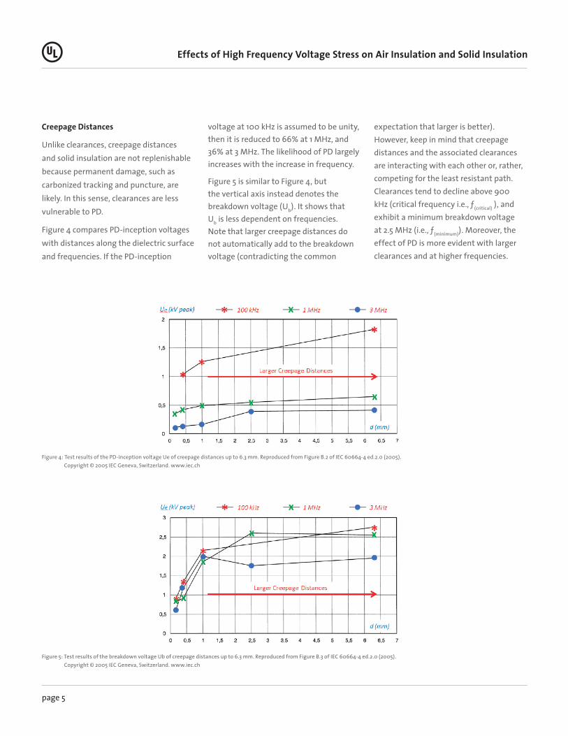
Figure 4: Test results of the PD-inception voltage Ue of creepage distances up to 6.3 mm. Reproduced from Figure B.2 of IEC 60664-4 ed.2.0 (2005). Copyright © 2005 IEC Geneva, Switzerland. www.iec.ch
Figure 5: Test results of the breakdown voltage Ub of creepage distances up to 6.3 mm. Reproduced from Figure B.3 of IEC 60664-4 ed.2.0 (2005). Copyright © 2005 IEC Geneva, Switzerland. www.iec.ch
Effects of High Frequency Voltage Stress on Air Insulation and Solid Insulation
page 5
Creepage Distances
Unlike clearances, creepage distances and solid insulation are not replenishable because permanent damage, such as carbonized tracking and puncture, are likely. In this sense, clearances are less vulnerable to PD.
Figure 4 compares PD-inception voltages with distances along the dielectric surface and frequencies. If the PD-inception
voltage at 100 kHz is assumed to be unity, then it is reduced to 66% at 1 MHz, and 36% at 3 MHz. The likelihood of PD largely increases with the increase in frequency.
Figure 5 is similar to Figure 4, but the vertical axis instead denotes the breakdown voltage (Ub). It shows that Ub is less dependent on frequencies. Note that larger creepage distances do not automatically add to the breakdown voltage (contradicting the common
expectation that larger is better). However, keep in mind that creepage distances and the associated clearances are interacting with each other or, rather, competing for the least resistant path. Clearances tend to decline above 900 kHz (critical frequency i.e., ƒ(critical) ), and exhibit a minimum breakdown voltage at 2.5 MHz (i.e., ƒ(minimum)). Moreover, the effect of PD is more evident with larger clearances and at higher frequencies.

Effects of High Frequency Voltage Stress on Air Insulation and Solid Insulation
page 6
All of this suggests that clearances are the leading cause of the phenomenon observed. Since charged ions travel along the electric field lines, any change in field direction could cause the ions to collide with, or be reflected away from, the dielectric surface. PD occurs in the clearances along the surface where the ionized gas is trapped, deteriorating carbon-based surface material, and making it more susceptible to carbonized tracking. This speculation also explains why the test results at 100 kHz are similar to those at 1MHz, but distinct from those at 3 MHz. The increased creepage distances are simply not able to compensate for the rapid deterioration of the associated clearances.
Solid Insulation
Compared to air insulation, solid insulation provides at least a ten-fold increase in electric strength. Influencing factors include insulation material thickness, temperature, and the duration of electrical stress. However, in practice, a PD can occur in embedded voids or air gaps in solid dielectrics at a PD-inception voltage far below its breakdown voltage, reducing its voltage withstand ability, and likely resulting in the complete destruction of nearly all solid dielectrics.
An electric field with a gas-filled void or an air gap is modeled in Figure 6. In the parallel plate model, the capacitance increases with the area of the plate
and the absolute permittivity of the dielectric (e.g., air is 1.006 times of ε0; polycarbonate is 2.3 times of ε0; FR-4 is 4.4 times of ε0) but decreases with the distance between the parallel plates. The capacitance of the remaining solid dielectric, C(remainder), is far greater than the capacitance of the void, C(void). Similarly, C(void) is far greater than the capacitance of the remaining solid dielectric connected in series with the void, C(series). As illustrated in equation (1), though the voltage across the void, V(void), does not seem to be greater than the voltage across C(series), it is still greater than any solid dielectric of the same size as the void, by a multiplier of the relative permittivity, εr.
Equation 1
Figure 6: Electric field distribution and equivalent circuit of electric field with a gas-filled void or an air gap
Effects of High Frequency Voltage Stress on Air Insulation and Solid Insulation
page 7
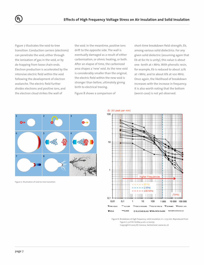
Figure 7 illustrates the void-to-tree transition. Conduction carriers (electrons) can penetrate the void, either through the ionization of gas in the void, or by de-trapping from loose chain ends. Electron production is accelerated by the intensive electric field within the void following the development of electron avalanche. The electric field further divides electrons and positive ions, and the electron cloud strikes the wall of
the void. In the meantime, positive ions drift to the opposite side. The wall is eventually damaged as a result of either carbonization, or ohmic heating, or both. After an elapse of time, the carbonized area shapes a ‘new’ void. As the new void is considerably smaller than the original, the electric field within the new void is stronger than before, ultimately giving birth to electrical treeing.
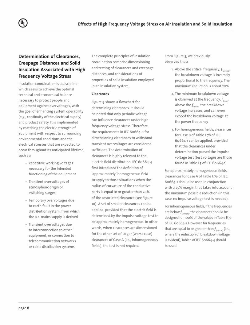
Figure 8 shows a comparison of
short-time breakdown field strength, Eb, among various solid dielectrics. For any given solid dielectric (assuming again that Eb at 60 Hz is unity), this value is about one- tenth at 1 MHz. With phenolic resin, for example, Eb is reduced to about 22% at 1 MHz, and to about 6% at 100 MHz. Once again, the likelihood of breakdown increases with the increase in frequency. It is also worth noting that the bottom (worst-case) is not yet observed.
Figure 7: Illustration of void-to-tree transition
Figure 8: Breakdown at high frequency, solid insulation; d = 0.75 mm. Reproduced from Figure C.3 of IEC 60664-4 ed.2.0 (2005). Copyright © 2005 IEC Geneva, Switzerland. www.iec.ch
Effects of High Frequency Voltage Stress on Air Insulation and Solid Insulation
page 8
Determination of Clearances, Creepage Distances and Solid Insulation Associated with High Frequency Voltage StressInsulation coordination is a discipline which seeks to achieve the optimal technical and economical balance necessary to protect people and equipment against overvoltages, with the goal of enhancing system operability (e.g., continuity of the electrical supply) and product safety. It is implemented by matching the electric strength of equipment with respect to surrounding environmental conditions and the electrical stresses that are expected to occur throughout its anticipated lifetime, such as:
• Repetitive working voltages necessary for the intended functioning of the equipment
• Transient overvoltages of atmospheric origin or switching surges
• Temporary overvoltages due to earth fault in the power distribution system, from which the a.c. mains supply is derived
• Transient overvoltages due to interconnection to other equipment, or connection to telecommunication networks or cable distribution systems
The complete principles of insulation coordination comprise dimensioning and testing of clearances and creepage distances, and considerations of properties of solid insulation employed in an insulation system.
Clearances
Figure 9 shows a flowchart for determining clearances. It should be noted that only periodic voltage can influence clearances under high frequency voltage stress. Therefore, the requirements in IEC 60664- 1 for dimensioning clearances to withstand transient overvoltages are considered sufficient. The determination of clearances is highly relevant to the electric field distribution. IEC 60664-4 first introduced the definition of ‘approximately’ homogeneous field to apply to those situations when the radius of curvature of the conductive parts is equal to or greater than 20% of the associated clearance (see Figure 10). A set of smaller clearances can be applied, provided that the electric field is determined by the impulse voltage test to be approximately homogeneous. In other words, when clearances are dimensioned for the other set of larger (worst-case) clearances of Case A (i.e., inhomogeneous fields), the test is not required.
From Figure 3, we previously observed that:
1. Above the critical frequency, ƒ(critical), the breakdown voltage is inversely proportional to the frequency. The maximum reduction is about 20%
2. The minimum breakdown voltage is observed at the frequency, ƒ(min). Above the ƒ(min), the breakdown voltage increases, and can even exceed the breakdown voltage at the power frequency
3. For homogeneous fields, clearances for Case B of Table F.7b of IEC 60664-1 can be applied, provided that the clearances under determination passed the impulse voltage test (test voltages are those found in Table F.5 of IEC 60664-1)
For approximately homogeneous fields, clearances for Case A of Table F.7a of IEC 60664-1 should be used in conjunction with a 25% margin that takes into account the maximum possible reduction (in this case, no impulse voltage test is needed).
For inhomogeneous fields, if the frequencies are below ƒ(critical), the clearances should be designed for 100% of the values in Table F.7a of IEC 60664-1. However, for frequencies that are equal to or greater than ƒ(critical) (i.e., where the reduction of breakdown voltage is evident), Table 1 of IEC 60664-4 should be used.

Effects of High Frequency Voltage Stress on Air Insulation and Solid Insulation
page 9
Figure 9: Flowchart for the determination of clearances
Figure 10: Examples of homogeneity of electric fields
Creepage Distances
Though the dimensioning of creepage distances is of little relevance to random transient overvoltages, it is commonly understood that the creepage distances must be equal to or greater than the
associated clearances.
Figure 11 shows a flowchart for determining creepage distances. In summary, for frequencies not exceeding 30 kHz, only the RMS-value of any periodic voltage is relevant. For
frequencies greater than 30 kHz, the dielectric breakdown resulting from the effects of PD has priority over the phenomenon of carbonized tracking, due to the accumulation of charges along the insulating surface.

Effects of High Frequency Voltage Stress on Air Insulation and Solid Insulation
page 10
Figure 11: Flowchart for determining creepage distances
Note that Table 2 of IEC 60664-4 only accounts for the PD-induced breakdown, and not the tracking phenomenon. Therefore, it is imperative to apply Table F.4 of IEC 60664-1 in conjunction Table 2 of IEC 60664-4.
Dimensioning creepage distances can be ignored if the surface material is not likely to be deteriorated by thermal effects (e.g., ceramics). However, dimensioning clearances still applies in such cases.
Solid Insulation
Because the breakdown field strength of solid insulation is higher than air insulation by at least one order of magnitude, the insulating distances through solid insulation can be much smaller than those for air insulation.
However, imperfect solid dielectric may contain gaps or voids, potentially initiating a PD at levels far below the breakdown voltage. Since PDs can degrade insulating material well in advance of its predicted useful life, good manufacturing practices and processes are imperative to reduce the likelihood of such breakdown.
The breakdown field strength of solid insulation can be generally represented as a function of the thickness of the material, and is also considerably influenced by environmental conditions such as heat and humidity. Verifying the adequacy of solid insulation is generally accomplished by conducting a performance-based test after environmental conditioning, since it
is difficult to calculate the thickness required to achieve the desired performance characteristics.
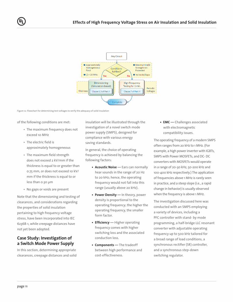
Figure 12 shows a flowchart for determining the test voltages necessary to verify the adequacy of solid insulation. High frequency testing includes a withstand test (short time stresses) and a PD test (long time stresses) to verify the integrity of solid insulation under high frequency voltage stress. Since a suitable test instrument is not readily available, a test similar to general power-frequency electric strength (hi-pot) test is considered as an acceptable alternative. Solid insulation can also be verified by dimensioning alone without performing high frequency testing, provided that all
Effects of High Frequency Voltage Stress on Air Insulation and Solid Insulation
page 11
Figure 12: Flowchart for determining test voltages to verify the adequacy of solid insulation
of the following conditions are met:
• The maximum frequency does not exceed 10 MHz
• The electric field is approximately homogeneous
• The maximum field strength does not exceed 2 kV/mm if the thickness is equal to or greater than 0.75 mm, or does not exceed 10 kV/mm if the thickness is equal to or less than 0.30 μm
• No gaps or voids are present
Note that the dimensioning and testing of clearances, and considerations regarding the properties of solid insulation pertaining to high frequency voltage stress, have been incorporated into IEC 62368-1, while creepage distances have not yet been adopted.
Case Study: Investigation of a Switch Mode Power SupplyIn this section, determining appropriate clearances, creepage distances and solid
insulation will be illustrated through the investigation of a novel switch mode power supply (SMPS), designed for compliance with various energy saving standards.
In general, the choice of operating frequency is achieved by balancing the following factors:
• Acoustic Noise — Ears can normally hear sounds in the range of 20 Hz to 20 kHz; hence, the operating frequency would not fall into this range (usually above 20 kHz).
• Power Density — In theory, power density is proportional to the operating frequency; the higher the operating frequency, the smaller form factor.
• Efficiency — Higher operating frequency comes with higher switching loss and the associated conduction loss.
• Components — The tradeoff between high performance and cost-effectiveness.
• EMC — Challenges associated with electromagnetic compatibility issues.
The operating frequency of a modern SMPS often ranges from 20 kHz to 1 MHz. (For example, a high power inverter with IGBTs, SMPS with Power MOSFETs, and DC- DC converters with MOSFETs would operate in a range of 20-30 kHz, 50-200 kHz and 100-400 kHz respectively.) The application of frequencies above 1 MHz is rarely seen in practice, and a steep slope (i.e., a rapid change in behavior) is usually observed when the frequency is above 1 MHz.
The investigation discussed here was conducted with an SMPS employing a variety of devices, including a PFC controller with stand- by mode programming, a half-bridge LLC resonant converter with adjustable operating frequency up to 500 kHz tailored for a broad range of load conditions, a synchronous rectifier (SR) controller, and a synchronous step-down switching regulator.
Effects of High Frequency Voltage Stress on Air Insulation and Solid Insulation
page 12
General technical information regarding the SMPS is as follows:
• Rated voltage range: 100-240 V a.c., 50/60 Hz
• Overvoltage category II: Pluggable equipment supplied by fixed electrical installation of buildings
• Pollution degree 2
• Peak working voltage: 514 V peak
• RMS working voltage: 270 V RMS
• Short-term temporary overvoltages: 1,440 V RMS, if it is intended to be supplied by IT or TT power system
• Operating frequency: 500 kHz
• Comparative tracking index (CTI): Material Group III
Clearances
1. Clearances to withstand transient overvoltages- Rated impulse voltage from Table F.1 of IEC 60664-1:
Nominal system voltage .......................................................................≤ 300 V a.c. Overvoltage category .............................................................................................. II Rated impulse voltage for equipment ..................................................... 2,500 V
- Clearances for Case A (inhomogeneous field) from Table F.2 of IEC 60664-1: Required impulse withstand voltage.................................................................... II Pollution degree......................................................................................................... 2 Clearances for basic insulation..................................................................... 1.5 mm Clearances for reinforced insulation ......................................................... 3.0 mm
Alternatively,- Impulse test voltage for verifying clearances from Table F.5 of IEC 60664-1:
Rated impulse voltage for equipment ..................................................... 2,500 V Impulse test voltage at sea level ............................................................... 2,920 V
- Clearances for Case B (homogeneous field) from Table F.2 of IEC 60664-1, upon the condition that the clearances are verified by the impulse test: Clearances for basic insulation................................................................... 0.6 mm Clearances for reinforced insulation ......................................................... 1.2 mm
2. Clearances to withstand periodic voltages (taken into account for high frequency voltage stress)
- Clearances for Case A (inhomogeneous field) from Table 1 of IEC 60664-4, upon the condition that the operating frequency is above ƒ(critical): Peak working voltage..........................................................................≤ 600 V peak Clearances for basic insulation.............................................................. 0.065 mm Clearances for reinforced insulation ...................................................... 0.50 mm

Effects of High Frequency Voltage Stress on Air Insulation and Solid Insulation
page 13
Alternatively,- Clearances for Case B (homogeneous field) from Table F.7 of IEC 60664-1,
upon the condition that the clearances are verified by the impulse test: Peak working voltage............................................................................... 514 V peak Clearances for basic insulation................................................................. 0.05 mm Clearances for reinforced insulation ........................................................ 0.11 mm
For clearances, the potential effect of transient overvoltages has priority over that of periodic voltages. Hence, the minimum clearance for basic insulation is 1.5 mm, and that for reinforced insulation is 3.0 mm. If the clearances are additionally verified by the impulse test, the minimum clearance for basic insulation and reinforced insulation can be reduced to 0.6 mm and 1.2 mm respectively.
Note that determining clearances to withstand periodic voltages does not account for short-term temporary overvoltages (TOV) of 1,440 V a.c., for the following reasons:
• The enormous offset (i.e., 1,200 V a.c.) is the product of the prospective high-voltage (HV) system earth fault current and the resistance of the earthing arrangement of the transformer substation, resulting in a highly-biased neutral. However, an offset of such magnitude can only occur in IT or TT power distribution systems where the earthing arrangements of the system and equipment are independent. In other words, TN system are immune to HV-system earth faults, and are only subject to faults in a low-voltage system at a maximum of 145% of the nominal line-to-neutral voltage
• If short-term temporary overvoltages (TOV) of 1,440 V a.c. (i.e., 2036 V peak) were taken into account, it would be impossible to obtain a reasonable value from Table 1 of IEC 60664-4, since Table 1 ends at 2,000 V peak, and extrapolation beyond that value is not allowed
• As the magnitude of the short-term TOV is much greater than the working voltages expected in current topologies of SMPSs, the measurement of working voltages is largely unnecessary
• It is questionable whether the SMPS would continue to generate artificial switch frequencies under such circumstances (highly-biased supply). Indeed, one could argue that the high frequency conditions would cease to exist after the equipment is damaged
Creepage Distances
1. Creepage distances to avoid carbonized tracking- Creepage distances from Table F.4 of IEC 60664-1:
RMS working voltage .......................................................................... 270 V r.m.s. Pollution degree......................................................................................................... 2 Comparative tracking index (CTI)............................................Material Group III Creepage distances for basic insulation ................................................... 2.7 mm Creepage distances for reinforced insulation.......................................... 5.4 mm
Effects of High Frequency Voltage Stress on Air Insulation and Solid Insulation
page 14
2. Creepage distances to avoid deterioration due to high frequency voltage stresses- Creepage distances from Table 2 of IEC 60664-4:
Peak working voltage.............................................................................. 514 V peak Pollution degree......................................................................................................... 2 Operating frequency ............................................................................... ≤ 500 kHz Creepage distances for basic insulation .................................................. 0.6 mm Creepage distances for reinforced insulation.......................................... 1.2 mm
For creepage distances, the effect of carbonized tracking takes priority over the effect of deterioration due to high frequency voltage stresses. Therefore, the minimum creepage distance for basic insulation is 2.7 mm, and that of reinforced insulation is 5.4 mm. No alignment is needed as the minimum creepage distances are greater than the minimum clearances.
Solid Insulation
1. Solid insulation verified by high frequency testing- A.C. high-frequency breakdown test verifying short-term dielectric
strength in accordance with Sub-clause 7.4 of IEC 60664-4: Peak working voltage............................................................................... 514 V peak Short-term temporary overvoltage ................................................... 2,211 V peak Test voltage for basic insulation.......................................................... 2,211 V peak Test voltage for reinforced insulation ..............................................4,422 V peak
- High-frequency partial discharge test verifying no partial discharge occur under steady-state conditions according to Sub-clause 7.5 of IEC 60664-4: Peak working voltage x 1.65 ..................................................................848 V peak Peak working voltage x 2.06 ...............................................................1060 V peak Long-term temporary overvoltage x 1.65 ......................................... 1,431 V peak Long-term temporary overvoltage x 2.06 ....................................... 1,789 V peak Test voltage for basic insulation.......................................................... 1,431 V peak Test voltage for reinforced insulation ............................................... 1,789 V peak
The following multiplying factors are applied in accordance with Sub- clause 6.1.3.5.1 of IEC 60664-1:
• F1 = 1.2: The basic safety factor for PD testing and dimensioning basic and supplementary insulation
• F2 = 1.25: PD hysteresis factor
• F3 = 1.25: The additional safety factor for PD testing and dimensioning reinforced insulation
• F4 = 1.1: The maximum deviation of the nominal voltage of the low-voltage system
• F1 x F2 x F4 = 1.65: Multiplying factor for basic and supplementary insulation
• F1 x F2 x F3 x F4 = 2.06: Multiplying factor for reinforced insulation
Effects of High Frequency Voltage Stress on Air Insulation and Solid Insulation
page 15
2. Solid insulation verified by method of dimensioning- Minimum thickness of solid insulation in accordance with to Sub-clause
6.3 of IEC 60664-1, upon all four aforesaid conditions are fulfilled: Required field strength for basic insulation .................................... 2,211 V peak Required field strength for reinforced insulation ........................ 4,422 V peak Required thickness for basic insulation ................................................. 0.46 mm Required thickness for reinforced insulation ........................................ 0.09mm
For solid insulation, the effect of a short-term temporary overvoltage takes priority over that of the highest steady-state voltage, the recurring peak voltages and the high frequency partial discharge. If all four of these conditions are met, high frequency testing is not needed, provided that the minimum thickness of the insulating material is not less than 0.46 mm for basic insulation, or not less than 0.09 mm for reinforced insulation. If any one of these conditions is not met, high frequency testing is necessary. For the a.c. high- frequency breakdown test, the test voltage is 2,211 V peak for basic insulation, and 4,422 V peak for reinforced insulation. For the high- frequency partial discharge test, the test voltage is 1,431 V peak for basic insulation, and 1,789 V peak for reinforced insulation.
A comparison between Different Product Safety StandardsInstead of a comprehensive comparison of the dimensioning of clearances, creepage distances and solid insulation found in IEC 62368-1 and the legacy standards (i.e., IEC 60950-1 and IEC 60065), this section offers a brief overview through a series of simplified charts.
Clearances
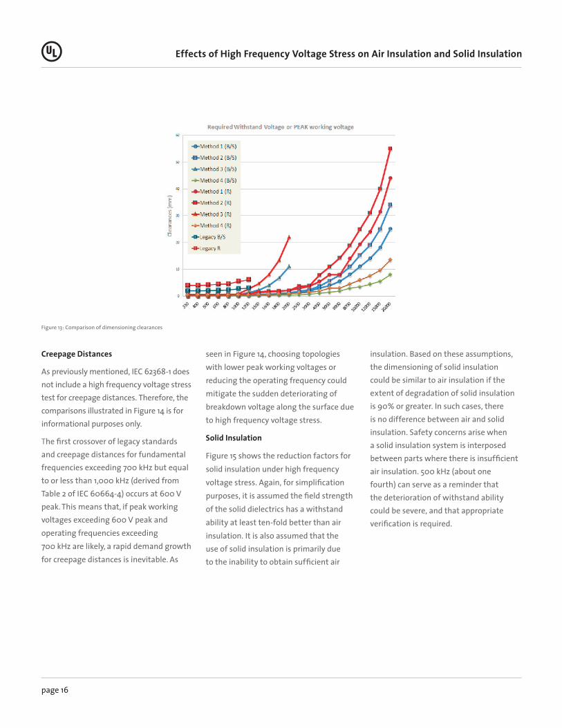
Figure 13 depicts a comparison of dimensioning clearances. In brief, the clearances of the legacy standards are obtained by assuming the a.c. mains supply does not exceed 300 V RMS (i.e., a.c. mains transient of 2,500 V peak, representing equipment designed for an universal input voltage range of 100-240 V a.c.), pollution degree 2, overvoltage category II. Hence, the traces of the legacy standards depicted result in an offset of 2 mm for basic or supplementary insulation, and 4 mm for reinforced insulation, and associated additional values in Table 2L of IEC 60950-1.
Figure 13 shows that, as long as the peak working voltages do not exceed 1,200 V peak, dimensioning according to the legacy standards will suffice for IEC 62368-1. In other words, for equipment with peak working voltage higher than that value, early awareness can mitigate the potential future impact on long-standing design practices.
Effects of High Frequency Voltage Stress on Air Insulation and Solid Insulation
page 16
Figure 13: Comparison of dimensioning clearances
Creepage Distances
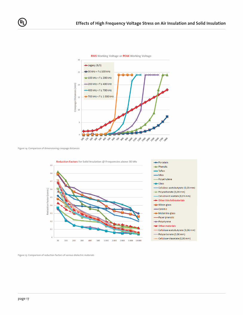
As previously mentioned, IEC 62368-1 does not include a high frequency voltage stress test for creepage distances. Therefore, the comparisons illustrated in Figure 14 is for informational purposes only.
The first crossover of legacy standards and creepage distances for fundamental frequencies exceeding 700 kHz but equal to or less than 1,000 kHz (derived from Table 2 of IEC 60664-4) occurs at 600 V peak. This means that, if peak working voltages exceeding 600 V peak and operating frequencies exceeding 700 kHz are likely, a rapid demand growth for creepage distances is inevitable. As
seen in Figure 14, choosing topologies with lower peak working voltages or reducing the operating frequency could mitigate the sudden deteriorating of breakdown voltage along the surface due to high frequency voltage stress.
Solid Insulation
Figure 15 shows the reduction factors for solid insulation under high frequency voltage stress. Again, for simplification purposes, it is assumed the field strength of the solid dielectrics has a withstand ability at least ten-fold better than air insulation. It is also assumed that the use of solid insulation is primarily due to the inability to obtain sufficient air
insulation. Based on these assumptions, the dimensioning of solid insulation could be similar to air insulation if the extent of degradation of solid insulation is 90% or greater. In such cases, there is no difference between air and solid insulation. Safety concerns arise when a solid insulation system is interposed between parts where there is insufficient air insulation. 500 kHz (about one fourth) can serve as a reminder that the deterioration of withstand ability could be severe, and that appropriate verification is required.
Effects of High Frequency Voltage Stress on Air Insulation and Solid Insulation
page 17
Figure 14: Comparison of dimensioning creepage distances
Figure 15: Comparison of reduction factors of various dielectric materials

Effects of High Frequency Voltage Stress on Air Insulation and Solid Insulation
page 18
ConclusionEmerging energy-saving standards have led to a marked preference for switch mode power supply topologies. However, the use of SMPSs has raised concerns over the sharp change in dielectric properties under high frequency voltage stress, and the attendant safety risks. This paper has provided some basic information about the partial discharge phenomena, and the rationale underlying the applicable product safety standards, in an effort to assist compliance engineers to better understand applicable testing requirements.
Acknowledgment
The author thanks the International Electrotechnical Commission (IEC) for permission to reproduce Information from its International Publication IEC 60664-4 ed.2.0 (2005). All such extracts are copyright of IEC, Geneva, Switzerland. All rights reserved. Further information on the IEC is available from www.iec.ch. IEC has no responsibility for the placement and context in which the extracts and contents are reproduced by the author, nor is IEC in any way responsible for the other content or accuracy therein.
For more information about the Effects of High Frequency Voltage Stress on Air Insulation and Solid Insulation white paper, please contact Flore Chiang, Senior Project Engineer, Consumer Sector, Conformity Assessment Services, [email protected].
UL and the UL logo are trademarks of UL LLC © 2012. No part of this document may be copied or distributed without the prior written consent of UL LLC 2012.
©2010 IEEE. Personal use of this material is permitted. However, permission to reprint/republish this material for advertising or promotional purposes or for creating new collective works for resale or redistribution to servers or lists, or to reuse any copyrighted component of this work in other works must be obtained from the IEEE.
1 Insulation Coordination for Equipment within Low-voltage Systems — Part 1: Principle, requirements and tests, IEC 60664-1, Second Edition, 2007
2 Insulation Coordination for Equipment within Low-voltage Systems — Part 4: Considerations of high-frequency voltage stress, IEC 60664-4, Second Edition, 2005
3 E. Kuffel, W.S. Zaengl, J. Kuffel, High Voltage Engineering Fundamentals, Second Edition. Newnes Oxford4 Audio/video, information and communication technology equipment — Part 1: Safety requirements, IEC 62368-1, First Edition, 2010,
including Corrigendum 1, 2010