Effect of Load Impedance on the Performance of …jaucs.com/issue39/E6.pdf · · 2016-12-27Effect...
31
Effect of Load Impedance on the Performance of Microwave… Firas M. Ali , Suhad H. Jasim Issue No. 39/2016 Journal of Al Rafidain University College 427 ISSN (1681-6870) Effect of Load Impedance on the Performance of Microwave Negative Resistance Oscillators Firas Mohammed Ali Al-Raie [email protected] University of Technology - Department of Electrical Engineering - Baghdad - Iraq Suhad Hussein Jasim [email protected] University of Technology - Department of Electrical Engineering - Baghdad - Iraq Abstract: In microwave negative resistance oscillators, the RF transistor presents impedance with a negative real part at either of its input or output ports. According to the conventional theory of microwave negative resistance oscillators, in order to sustain oscillation and optimize the output power of the circuit, the magnitude of the negative real part of the input/output impedance should be maximized. This paper discusses the effect of the circuit’s load impedance on the input negative resistance and other oscillator performance characteristics in common base microwave oscillators. New closed-form relations for the optimum load impedance that maximizes the magnitude of the input negative resistance have been derived analytically in terms of the Z- parameters of the RF transistor. Furthermore, nonlinear CAD simulation is carried out to show the deviation of the large-signal
Transcript of Effect of Load Impedance on the Performance of …jaucs.com/issue39/E6.pdf · · 2016-12-27Effect...
Effect of Load Impedance on the Performance of Microwave…
Firas M. Ali , Suhad H. Jasim Issue No. 39/2016
Journal of Al Rafidain University College 427 ISSN (1681-6870)
Effect of Load Impedance on the Performance of
Microwave Negative Resistance Oscillators
Firas Mohammed Ali Al-Raie [email protected]
University of Technology - Department of Electrical
Engineering - Baghdad - Iraq
Suhad Hussein Jasim [email protected]
University of Technology - Department of Electrical
Engineering - Baghdad - Iraq
Abstract: In microwave negative resistance oscillators, the RF
transistor presents impedance with a negative real part at either of
its input or output ports. According to the conventional theory of
microwave negative resistance oscillators, in order to sustain
oscillation and optimize the output power of the circuit, the
magnitude of the negative real part of the input/output impedance
should be maximized. This paper discusses the effect of the circuit’s
load impedance on the input negative resistance and other
oscillator performance characteristics in common base microwave
oscillators. New closed-form relations for the optimum load
impedance that maximizes the magnitude of the input negative
resistance have been derived analytically in terms of the Z-
parameters of the RF transistor. Furthermore, nonlinear CAD
simulation is carried out to show the deviation of the large-signal
Effect of Load Impedance on the Performance of Microwave…
Firas M. Ali , Suhad H. Jasim Issue No. 39/2016
Journal of Al Rafidain University College 428 ISSN (1681-6870)
optimum load impedance from its small-signal value. It has been
shown also that the optimum load impedance for maximum
negative input resistance differs considerably from its value
required for maximum output power under large-signal conditions.
A 1.8 GHz oscillator circuit has been designed and simulated using
a typical SiGe hetero-junction bipolar transistor (HBT) to verify the
proposed approach of analysis.
Keywords: Negative Resistance Oscillators, Common Base
Oscillator, Microwave Nonlinear Circuits, SiGe HBT Transistors.
1. Introductory Concepts
RF and microwave oscillators are fundamental elements in
different wireless communication systems. Basically, there are two
approaches for the analysis of RF oscillators: the open-loop gain
approach [1, 2] and the negative resistance approach [3, 4].
In the open-loop gain method, the oscillator circuit is viewed to
be composed of an amplifier cascaded with a resonator. The open
loop gain, S21, of the combination is evaluated and tested across a
frequency range around the desired oscillation frequency. The
necessary conditions for starting the oscillation is that the phase of
S21 should equal to zero, while there is a considerable gain margin
at the frequency of oscillation [5]. When the loop is closed, the
output signal builds until reaching a steady state condition where
the gain becomes 0 dB as the RF device enters the nonlinear region.
This causes shift in the oscillation frequency and other performance
characteristics and therefore the design approach should be
modified under large-signal conditions.
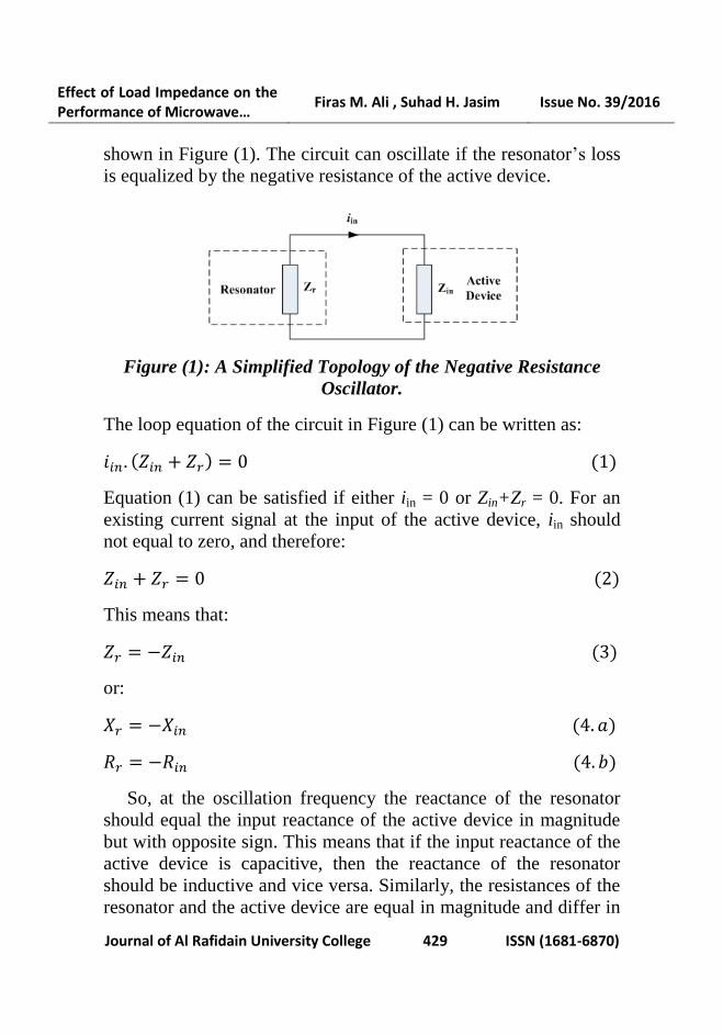
On the other hand, in negative resistance oscillators the RF
device is characterized as a one-port network by its input
impedance Zin and is connected with a resonator of impedance Zr as
Effect of Load Impedance on the Performance of Microwave…
Firas M. Ali , Suhad H. Jasim Issue No. 39/2016
Journal of Al Rafidain University College 429 ISSN (1681-6870)
shown in Figure (1). The circuit can oscillate if the resonator’s loss
is equalized by the negative resistance of the active device.
Figure (1): A Simplified Topology of the Negative Resistance
Oscillator.
The loop equation of the circuit in Figure (1) can be written as:
𝑖𝑖𝑛. (𝑍𝑖𝑛 + 𝑍𝑟) = 0 (1)
Equation (1) can be satisfied if either iin = 0 or Zin+Zr = 0. For an
existing current signal at the input of the active device, iin should
not equal to zero, and therefore:
𝑍𝑖𝑛 + 𝑍𝑟 = 0 (2)
This means that:
𝑍𝑟 = −𝑍𝑖𝑛 (3)
or:
𝑋𝑟 = −𝑋𝑖𝑛 (4. 𝑎)
𝑅𝑟 = −𝑅𝑖𝑛 (4. 𝑏)
So, at the oscillation frequency the reactance of the resonator
should equal the input reactance of the active device in magnitude
but with opposite sign. This means that if the input reactance of the
active device is capacitive, then the reactance of the resonator
should be inductive and vice versa. Similarly, the resistances of the
resonator and the active device are equal in magnitude and differ in

Effect of Load Impedance on the Performance of Microwave…
Firas M. Ali , Suhad H. Jasim Issue No. 39/2016
Journal of Al Rafidain University College 430 ISSN (1681-6870)
sign. But since the resonator is a passive circuit then its resistance is
positive in all conditions, and therefore the active device should
present a negative resistance at the oscillation frequency.
The input resistance and reactance of the active device are not
solely functions of the frequency but vary also with the power level
at the input port of the device. So, the large signal magnitude of Rin
is different from its small signal value due to the inherent
nonlinearities in the active device. This resistance usually decreases
with power level in most practical RF devices as shown in Figure
(2) [6]. In this sketch, the value of the small signal input resistance
equals to -Ro, while Pin represents the available power at the input
port, and Pth is the threshold input power at which the large-signal
device’s input resistance deviates from its small-signal value.
Figure (2): Typical Variation of Negative Input Resistance with
Power Level.
So, the necessary condition for oscillation is to make Rr less than
the magnitude of the small-signal input resistance in order to place
the operating point beyond threshold:
𝑅𝑟 < |𝑅𝑜| (5)

Effect of Load Impedance on the Performance of Microwave…
Firas M. Ali , Suhad H. Jasim Issue No. 39/2016
Journal of Al Rafidain University College 431 ISSN (1681-6870)
The resonator resistance Rr is usually taken equal to |Ro|/3 as a
practical rule of thumb for the startup of oscillation [6].
2. Related Work
The fundamental concepts of negative resistance microwave
oscillators were established by Kurokawa’s work [3,7]. He
developed the steady state oscillation condition of the oscillator
circuit. Further studies were concentrated on the use of large signal
S-parameters to maximize the output power and efficiency for
microwave oscillators [8-10]. Analytic derivation of the large-
signal S-parameters in terms of the input and output device terminal
voltage amplitudes was carried out [11]. These equations are
formulated systematically as a root finder computer algorithm to
determine the circuit elements for maximum oscillator’s output
power.
Another technique for the evaluation of different oscillator
circuit topologies for optimized output power was carried out
depending on the measurements of an optimized power amplifier
[12]. This technique takes benefits from the ease of power amplifier
measurements when compared with oscillator’s measurement. A
simplified quasi-linear design technique for GaAs MESFET
oscillators was also developed [13]. In this approach the generated
oscillator’s power is derived in terms of the gate and drain RF
voltages. The oscillator circuit elements are derived to maximize
the generated power under the limiting conditions of the terminal
voltage amplitudes.
An analytical approach to the design of microwave oscillators
with output power prediction was documented [14]. This design
method is mainly concerned with the calculation of the oscillator’s
network elements using small-signal RF device two-port
parameters as the starting point. The oscillator output power is
estimated with the aid of the DC bias voltage and current. A
linearized design method that maximizes the added power in a two-

Effect of Load Impedance on the Performance of Microwave…
Firas M. Ali , Suhad H. Jasim Issue No. 39/2016
Journal of Al Rafidain University College 432 ISSN (1681-6870)
port oscillator was verified [15]. In this technique, different
network topologies are analyzed for the sake of optimized output
power with the RF device modeled through its small-signal
parameters.
Andrei Grebennikov proved analytically that maximum
output power of the RF oscillator can be obtained by maximizing
the negative real part of the output impedance of the RF device, and
derived expressions for the optimum circuit elements based on this
assumption [16]. This technique was applied both to BJT [17] and
FET [18] oscillator circuits. Microstrip resonators were also used in
negative resistance microwave oscillator circuits employing either
GaAs FET or bipolar devices [19].
Emitter degeneration technique was applied to increase the
oscillation frequency and improve the phase noise and tuning range
of RF oscillators [20]. The frequency tuning capability of RF
oscillators is performed by inserting varactor diodes in the
resonator circuits [21].
A method for designing negative resistance RF oscillators
based on large-signal measurement setup was verified [22]. In this
technique, measurements are performed based on the real-time
active load-pull (RTALP) method for the second and third
harmonics using a large-signal network analyzer (LSNA). A novel
technique was presented to increase the negative resistance and
thereby the output power for common collector Colpitts oscillators
by means of an inductor [23]. The inductance value is selected to
overcome the parasitic capacitances of the collector-base and
emitter-base junctions. Another measurement-based design
technique for negative resistance microwave oscillators has been
proposed [24]. According to this technique, a harmonic-loaded
oscillator can be efficiently designed at the specified frequency
using a novel multi-harmonic real-time active load-pull technique.
Using this methodology, a stable negative resistance RF transistor
active circuit is first optimized with the aid of computer simulations
around the desired frequency. The optimal second- and third-

Effect of Load Impedance on the Performance of Microwave…
Firas M. Ali , Suhad H. Jasim Issue No. 39/2016
Journal of Al Rafidain University College 433 ISSN (1681-6870)
harmonic load impedances that achieve maximum output power are
then extracted. The loading network of the oscillator can thereby be
synthesized to present the measured optimal harmonic impedances
at the device’s output port.
To overcome the limitations of the small-signal scattering
parameters in predicting the performance behavior of RF oscillators
under nonlinear conditions, improved analytical expressions based
on large-signal X-parameters have been developed for use in
transistor oscillator circuit design [25].
In another recent study, it was shown that increasing the
magnitude of the negative output resistance of the RF device does
not always lead to greater output power [26]. Finally, the stability
analysis of negative resistance oscillators has been analyzed based
on X-parameters which provide significant behavioral modeling for
the circuit under large-signal conditions [27].
3. Potentially Unstable Active Devices
In order to achieve a negative resistance at one of the RF
transistor ports, it should be placed in the unstable region. In other
words, the RF transistor should be potentially unstable at the
desired frequency of oscillation which means that its stability
factor, K, is less than one, where K can be expressed in terms of Z-
parameters as [28]:
𝐾 =2𝑅11𝑅22 − 𝑅𝑒[𝑍12𝑍21]
|𝑍12𝑍21| (6)
Where: R11 = Re[Z11], R22 = Re[Z22], and Zij are the Z-parameters of
the RF transistor at the specific frequency.
The oscillation susceptibility of the RF transistor can be
increased by connecting it in common base configuration. The
instability region of the common base configuration can further be
extended by adding an additional feedback element as illustrated in

Effect of Load Impedance on the Performance of Microwave…
Firas M. Ali , Suhad H. Jasim Issue No. 39/2016
Journal of Al Rafidain University College 434 ISSN (1681-6870)
Figure (3), where an inductor is inserted in the base terminal to
constitute a series feedback network [29]. The inductance value can
either be calculated analytically using a simplified equivalent
circuit model for the RF device, or can be optimized using a
microwave CAD simulator. The load stability circle of the RF
transistor is first sketched on the Smith chart to view the unstable
region for all possible load reflection coefficient values. If the
stability circle does not cover a considerable part of the Smith
chart, then the circuit presented in Figure (3) should be selected to
extend the unstable region.
Figure (3): Common Base Configurations with Series Base
Inductance.
4. Analytic Determination of the Optimum Load
Impedance
A block diagram for the negative resistance oscillator is
presented in Figure (4). It consists of an active device with certain
positive feedback and is terminated by the resonator at its input
port, and a load at its output port. The output matching network is
necessary to present the required load impedance ZL at the output
port. The loading effect at the output port greatly affects the value
of the input impedance Zin. In order to make the circuit oscillate, the
real part of the input impedance should be made negative. To
obtain maximum power at the load terminal, the magnitude of the
negative input resistance of the RF device is maximized [16]. So,

Effect of Load Impedance on the Performance of Microwave…
Firas M. Ali , Suhad H. Jasim Issue No. 39/2016
Journal of Al Rafidain University College 435 ISSN (1681-6870)
the optimum load impedance ZL(opt) can be selected to maximize the
magnitude of the negative real part of the input impedance.
Figure (4): A Block Diagram for the Negative Resistance
Oscillator.
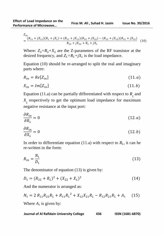
It is convenient to analytically determine ZL=RL+jXL which
is required to make |Rin| maximum. This can be done by evaluating
an equation for Rin and partial differentiating it with respect to RL
and XL respectively after characterizing the active device with its Z-
parameters at the required frequency.
From two-port network theory, if the device is described in
terms of its Z-parameters then the input impedance is given by:
𝑍𝑖𝑛 = 𝑍11 −𝑍12. 𝑍21
𝑍22 + 𝑍𝐿
(7)
After some arrangement,
𝑍𝑖𝑛 =𝑍11. 𝑍𝐿 + ∆𝑧
𝑍22 + 𝑍𝐿
(8)
where:
∆𝑧= 𝑍11. 𝑍22 − 𝑍12. 𝑍21 (9)
Equation (8) can be re-written as:
Effect of Load Impedance on the Performance of Microwave…
Firas M. Ali , Suhad H. Jasim Issue No. 39/2016
Journal of Al Rafidain University College 436 ISSN (1681-6870)
𝑍𝑖𝑛
=(𝑅11 + 𝑗𝑋11)(𝑅𝐿 + 𝑗𝑋𝐿) + (𝑅11 + 𝑗𝑋11)(𝑅22 + 𝑗𝑋22) − (𝑅12 + 𝑗𝑋12)(𝑅21 + 𝑗𝑋21)
𝑅22 + 𝑗𝑋22 + 𝑅𝐿 + 𝑗𝑋𝐿
(10)
Where: Zij=Rij+Xij are the Z-parameters of the RF transistor at the
desired frequency, and ZL=RL+jXL is the load impedance.
Equation (10) should be re-arranged to split the real and imaginary
parts where:
𝑅𝑖𝑛 = 𝑅𝑒[𝑍𝑖𝑛] (11. 𝑎)
𝑋𝑖𝑛 = 𝐼𝑚[𝑍𝑖𝑛] (11. 𝑏)
Equation (11.a) can be partially differentiated with respect to RL
and
XL
respectively to get the optimum load impedance for maximum
negative resistance at the input port:
𝜕𝑅𝑖𝑛
𝜕𝑅𝐿
= 0 (12. 𝑎)
𝜕𝑅𝑖𝑛
𝜕𝑋𝐿
= 0 (12. 𝑏)
In order to differentiate equation (11.a) with respect to RL, it can be
re-written in the form:
𝑅𝑖𝑛 =𝑁1
𝐷1
(13)
The denominator of equation (13) is given by:
𝐷1 = (𝑅22 + 𝑅𝐿)2 + (𝑋22 + 𝑋𝐿)2 (14)
And the numerator is arranged as:
𝑁1 = 2 𝑅11𝑅22𝑅𝐿 + 𝑅11𝑅𝐿2 + 𝑋12𝑋21𝑅𝐿 − 𝑅12𝑅21𝑅𝐿 + 𝐴1 (15)
Where A1 is given by:

Effect of Load Impedance on the Performance of Microwave…
Firas M. Ali , Suhad H. Jasim Issue No. 39/2016
Journal of Al Rafidain University College 437 ISSN (1681-6870)
𝐴1 = 𝑅11𝑅222 − 𝑅12𝑅21𝑅22 + 2𝑅11𝑋22𝑋𝐿 + 𝑅11𝑋22
2 + 𝑅11𝑋𝐿2 − 𝑅12𝑋21𝑋22
− 𝑅12𝑋21𝑋𝐿 − 𝑅21𝑋12𝑋22 − 𝑅21𝑋12𝑋𝐿 + 𝑅22𝑋12𝑋21 (16)
Applying equation (12.a) and rearranging yields:
𝑅𝐿(𝑜𝑝𝑡) =−𝛼2 + √𝛼2
2 − 4𝛼1𝛼3
2𝛼1
(17)
where:
𝛼1 = 2𝑅11𝑅22 + 2𝑅12𝑅21 − 2𝑋12𝑋21 + 𝐴3 (18)
𝛼2 = 2𝑅12𝑅21𝑅22 − 4𝑅11𝑅222 − 2𝑅22𝑋12𝑋21 + 2𝑅11𝐴2 + 2𝑅22𝐴3
− 2𝐴1 (19)
𝛼3 = 𝐴2𝐴3 − 2𝑅22𝐴1 (20)
𝐴2 = 𝑅222 + 𝑋22
2 + 2𝑋22𝑋𝐿 + 𝑋𝐿2 (21)
𝐴3 = 2𝑅11𝑅22 − 𝑅12𝑅21 + 𝑋12𝑋21 (22)
Equation (17) is derived in terms of the transistor Z-parameters and
the load reactance XL.
Similarly, in order to differentiate equation (11.a) with respect to
XL, it can be re-written in the form:
𝑅𝑖𝑛 =𝑁2
𝐷2
(23)
The denominator of equation (23) is given by:
𝐷2 = (𝑅22 + 𝑅𝐿)2 + (𝑋22 + 𝑋𝐿)2 (24)
and the numerator is arranged as:
𝑁2 = 2 𝑅11𝑋22𝑋𝐿 + 𝑅11𝑋𝐿2 − 𝑅12𝑋21𝑋𝐿 − 𝑅21𝑋12𝑋𝐿 + 𝐵1 (25)
Where B1 is given by:

Effect of Load Impedance on the Performance of Microwave…
Firas M. Ali , Suhad H. Jasim Issue No. 39/2016
Journal of Al Rafidain University College 438 ISSN (1681-6870)
𝐵1 = 2𝑅11𝑅22𝑅𝐿 + 𝑅11𝑅222 + 𝑅11𝑅𝐿
2 − 𝑅12𝑅21𝑅22 − 𝑅12𝑅21𝑅𝐿
− 𝑅12𝑋21𝑋22 − 𝑅21𝑋12𝑋22 + 𝑅22𝑋12𝑋21 + 𝑅𝐿𝑋12𝑋21 (26)
Applying equation (12.b) and rearranging leads to:
𝑋𝐿(𝑜𝑝𝑡) =−𝛽2 + √𝛽2
2 − 4𝛽1𝛽3
2𝛽1
(27)
where:
𝛽1 = 2𝑅12𝑋21 − 2𝑅11𝑋22 − 2𝑅21𝑋12 + 𝐵3 (28)
𝛽2 = 2𝑅11𝐵2 − 4𝑅11𝑋222 + 2𝑅12𝑋21𝑋22 + 2𝑅21𝑋12𝑋22 + 2𝑋22𝐵3
− 2𝐵1 (29)
𝛽3 = 𝐵2𝐵3 − 2𝐵1𝑋22 (30)
𝐵2 = 𝑅222 + 2𝑅22𝑅𝐿 + 𝑅𝐿
2 + 𝑋222 (31)
𝐵3 = 2𝑅11𝑋22 − 𝑅12𝑋21 − 𝑅21𝑋12 (32)
The real part of the input impedance (Rin) can be calculated
either from equation (13) or (23), while the imaginary part of the
input impedance (Xin) can be evaluated in terms of RL(opt) and XL(opt)
where:
𝑋𝑖𝑛 =𝑁3
𝐷3
(33)
where:
𝐷3 = (𝑅22 + 𝑅𝐿)2 + (𝑋22 + 𝑋𝐿)2 (34)
and
𝑁3 = 2𝑅22𝑅𝐿𝑋11 + 𝑅222𝑋11 + 𝑅12𝑅21𝑋22 + 𝑅12𝑅21𝑋𝐿
− 𝑅12𝑅22𝑋21 − 𝑅21𝑅22𝑋12 − 𝑅12𝑅𝐿𝑋21 − 𝑅21𝑅𝐿𝑋12
+ 𝑅𝐿2𝑋11 + 2𝑋11𝑋22𝑋𝐿 + 𝑋11𝑋22
2 + 𝑋11𝑋𝐿2
− 𝑋12𝑋21𝑋22 − 𝑋12𝑋21𝑋𝐿 (35)

Effect of Load Impedance on the Performance of Microwave…
Firas M. Ali , Suhad H. Jasim Issue No. 39/2016
Journal of Al Rafidain University College 439 ISSN (1681-6870)
The derived equations for RL(opt) and XL(opt) apply for small-
signal power levels before threshold . But in practice since Rin is a
function of signal level as depicted in Figure (2), the optimum load
resistance RL(opt) and optimum load reactance XL(opt) may vary with
power level. RL(opt) and XL(opt) can thus be found from large-signal
simulation of the circuit at the desired oscillator’s power level and
frequency using the non-linear model of the transistor to generate a
family of curves for Rin, |Γin
|, power gain, and output power as
functions of both RL and XL. A compromise is to be done for
important oscillator performance characteristics such as high output
power, low harmonic distortion, minimal stability factor, and high
resonator’s quality factor when selecting RL and XL from the
generated curves.
5. Design of a 1.8 GHz Oscillator Circuit
A microwave oscillator circuit is to be designed and
simulated in order to verify the effect of load impedance on its
performance characteristics. This circuit operates at the standard
1800 MHz mobile communication band (GSM-1800). Desired
specifications are to achieve an output power of more than 10 dBm,
second harmonic distortion level better than -20 dBc, and low phase
noise at 1.8 GHz.
5.1 Selection of the RF Transistor
SiGe heterojunction bipolar transistors (HBTs) are improved
versions of BJT transistors with superior high frequency
performance characteristics. The structure is similar to that of the
silicon transistor but the base region is incorporated with
germanium. The addition of germanium to the base region reduces
its resistance and transit time, which increases the transition
frequency fT [30]. The higher base doping concentration reduces
also the noise figure of the transistor [31].
In this design, the NPN SiGe heterojunction bipolar
transistor NESG2101M05 of Renesas (Previously NEC) has been

Effect of Load Impedance on the Performance of Microwave…
Firas M. Ali , Suhad H. Jasim Issue No. 39/2016
Journal of Al Rafidain University College 440 ISSN (1681-6870)
selected. This device is a low power transistor and has low noise
figure in the order of 0.9 dB at 2 GHz with an associated power
gain of 13 dB. It has a typical transition frequency fT of 17 GHz.
The transistor is to be biased at VCE = 3 V and IC = 20 mA. The DC
simulation of the large-signal model of the transistor indicates that
VBE = 0.835 V for a collector current of 20 mA with a DC current
gain, hFE, of 185.
5.2 Large Signal Z-Parameters and Stability Evaluation
The test circuit for viewing the stability conditions and
extracting the large-signal device parameters is shown in Figure
(5). The transistor is connected in common base configuration, and
a bias circuit is designed to place the Q-point at VCE = 3V and IC =
20 mA. The input power level is varied from -20 dBm to +15 dBm
and the simulation frequency is set at 1.8 GHz. The circuit has been
simulated using the harmonic balance algorithm provided by the
nonlinear microwave CAD program ADS 2009 of Keysight
Technologies.
Figure (5): Simulation Setup for Large Signal Z-Parameters
Extraction.
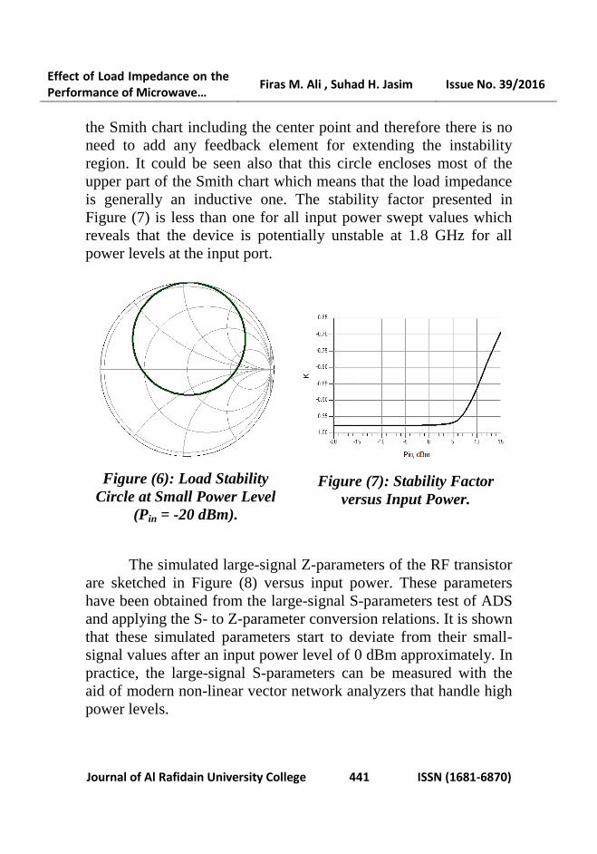
The load stability circle is sketched in Figure (6) and is
measured at a small-signal input power level of -20 dBm, while
Figure (7) presents the stability factor, K, versus input power. As
shown from Figure (6), the stability circle covers a large portion of
Effect of Load Impedance on the Performance of Microwave…
Firas M. Ali , Suhad H. Jasim Issue No. 39/2016
Journal of Al Rafidain University College 441 ISSN (1681-6870)
the Smith chart including the center point and therefore there is no
need to add any feedback element for extending the instability
region. It could be seen also that this circle encloses most of the
upper part of the Smith chart which means that the load impedance
is generally an inductive one. The stability factor presented in
Figure (7) is less than one for all input power swept values which
reveals that the device is potentially unstable at 1.8 GHz for all
power levels at the input port.
Figure (6): Load Stability
Circle at Small Power Level
(Pin = -20 dBm).
Figure (7): Stability Factor
versus Input Power.
The simulated large-signal Z-parameters of the RF transistor
are sketched in Figure (8) versus input power. These parameters
have been obtained from the large-signal S-parameters test of ADS
and applying the S- to Z-parameter conversion relations. It is shown
that these simulated parameters start to deviate from their small-
signal values after an input power level of 0 dBm approximately. In
practice, the large-signal S-parameters can be measured with the
aid of modern non-linear vector network analyzers that handle high
power levels.

Effect of Load Impedance on the Performance of Microwave…
Firas M. Ali , Suhad H. Jasim Issue No. 39/2016
Journal of Al Rafidain University College 442 ISSN (1681-6870)
(a) Z11
(b) Z12
(c) Z21
(d) Z22
Figure (8): Large Signal Z-parameters of the RF Transistor.
5.3 Simulation of Load Impedance Variations
In order to simulate the effect of the load impedance on the
negative input resistance and output power of the oscillator, the
simulation setup of Figure (5) has been modified by maintaining
the input power level at a certain value and changing the load
impedance ZL, where ZL= RL + jXL. Figure (9-a) presents the
variation of the input resistance of the RF device with load
reactance XL for three values of RL with input power of -20 dBm
(small-signal condition), while Figure (9-b) shows the equivalent
variation of the output power with XL.

Effect of Load Impedance on the Performance of Microwave…
Firas M. Ali , Suhad H. Jasim Issue No. 39/2016
Journal of Al Rafidain University College 443 ISSN (1681-6870)
(a) Rin versus XL
(b) Pout versus XL
Figure (9): Variation of Input Resistance (a) and Output Power
(b) versus Load Reactance for Three Different Values of RL when
Pin = -20 dBm.
In Figure 10, the variations of Rin and Pout with XL are
sketched with Pin = 0 dBm (large-signal condition), while Figure 11
presents the corresponding variations for Pin = 3 dBm (very large-
signal condition).
(a) Rin versus XL
(b) Pout versus XL
Figure (10): Variation of Input Resistance (a) and Output Power
(b) versus Load Reactance for Three Different Values of RL when
Pin = 0 dBm.
Effect of Load Impedance on the Performance of Microwave…
Firas M. Ali , Suhad H. Jasim Issue No. 39/2016
Journal of Al Rafidain University College 444 ISSN (1681-6870)
(a) Rin versus XL
(b) Pout versus XL
Figure (11): Variation of Input Resistance (a) and Output Power
(b) versus Load Reactance for Three Different Values of RL when
Pin = 3 dBm.
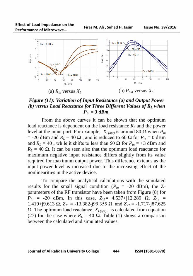
From the above curves it can be shown that the optimum
load reactance is dependent on the load resistance RL and the power
level at the input port. For example, XL(opt) is around 80 Ω when Pin
= -20 dBm and RL = 40 Ω , and is reduced to 60 Ω for Pin = 0 dBm
and RL = 40 , while it shifts to less than 50 Ω for Pin = +3 dBm and
RL = 40 Ω. It can be seen also that the optimum load reactance for
maximum negative input resistance differs slightly from its value
required for maximum output power. This difference extends as the
input power level is increased due to the increasing effect of the
nonlinearities in the active device.
To compare the analytical calculations with the simulated
results for the small signal condition (Pin = -20 dBm), the Z-
parameters of the RF transistor have been taken from Figure (8) for
Pin = -20 dBm. In this case, Z11= 4.537+j12.289 Ω, Z12 =
1.419+j9.613 Ω, Z21 = -13.382-j99.355 Ω, and Z22 = -1.717-j87.625
Ω. The optimum load reactance, XL(opt), is calculated from equation
(27) for the case where RL = 40 Ω. Table (1) shows a comparison
between the calculated and simulated values.

Effect of Load Impedance on the Performance of Microwave…
Firas M. Ali , Suhad H. Jasim Issue No. 39/2016
Journal of Al Rafidain University College 445 ISSN (1681-6870)
Table (1): Calculated and Simulated Values of XL(opt) and Zin for
RL = 40 Ω.
Parameter
Calculated
Value
(Small-Signal)
Simulated
Value for
Pin = -20 dBm
Simulated
Value for
Pin = 0 dBm
Simulated
Value for
Pin = +3 dBm
XL(opt), Ω 82.22 82 60 46
Rin, Ω -20.14 -20.39 -13.47 -8.83
Xin, Ω 15.81 15.70 7.84 4.91
As shown from Table (1), the calculated value of XL(opt) is
very close to the simulated value for the small-signal condition (Pin
= -20 dBm). However, as power level is increased, the optimum
load reactance deviates considerably from its small-signal
calculated value. This means that for a successful oscillator design,
the optimum load impedance must be chosen specifically for the
specified output power level and the corresponding power level at
the input port. Similarly, the negative input resistance and output
power can be varied with RL for a given value of XL. Figure (12)
shows this variation for a small-signal input power level of -20
dBm and three different values of XL. The optimum load resistance
required to obtain maximum negative input resistance is around 15
Ω for XL = 70 Ω as depicted from Figure (12-a), while its value is
about 19 Ω for maximum output power with XL = 70 Ω. It is clear
from Figure (9) that the optimum load reactance for this input
power level is about 80 Ω. So, the optimum load impedance for this
power level is thus ZL = 19+j80 Ω.

Effect of Load Impedance on the Performance of Microwave…
Firas M. Ali , Suhad H. Jasim Issue No. 39/2016
Journal of Al Rafidain University College 446 ISSN (1681-6870)
(a) Rin versus RL
(b) Pout versus RL
Figure (12): Variation of Input Resistance (a) and Output Power
(b) versus Load Resistance for Three Different Values of XL when
Pin = -20 dBm.
(a) Rin versus RL
(b) Pout versus RL
Figure (13): Variation of Input Resistance (a) and Output Power
(b) versus Load Resistance for Three Different Values of XL when
Pin = 0 dBm.
In Figure (13), Rin and Pout are sketched versus RL for
different values of XL with increasing the input power level to 0
dBm. It is noticed that there is a considerable change from the
results obtained for the small signal simulation in Figure (12). The
optimum load resistance for maximum Rin is about 32 Ω with XL =
60 Ω. Its value is reduced to 28 Ω for maximum Pout. From Figure
(10), it was found that the optimum load reactance is about 60 Ω.
So, the optimum load impedance for a maximum power level is ZL

Effect of Load Impedance on the Performance of Microwave…
Firas M. Ali , Suhad H. Jasim Issue No. 39/2016
Journal of Al Rafidain University College 447 ISSN (1681-6870)
= 28+j60 Ω, and the maximum attainable power in this case is
about 14.5 dBm given that Pin = 0 dBm.
In Figure (14), the simulations are repeated for Pin = 3 dBm.
It is noticed that the optimum load resistance is increased, while the
magnitude of the negative input resistance is significantly
decreased. The maximum attainable power in this case becomes
about 14.85 dBm which is not far away from the value obtained
under the condition of Pin = 0 dBm. This means that the RF device
enters saturation at this power level which may increase the
distortion level in the output signal.
(a) Rin versus RL
(b) Pout versus RL
Figure (14): Variation of Input Resistance (a) and Output Power
(b) versus Load Resistance for Three Different Values of XL when
Pin = 3 dBm.
Table (2) summarizes the variation in the optimum load
resistance with power level for XL = 60 Ω. The optimum load
resistance and input impedance differ significantly for large-signal
levels when compared with their small-signal calculated values.

Effect of Load Impedance on the Performance of Microwave…
Firas M. Ali , Suhad H. Jasim Issue No. 39/2016
Journal of Al Rafidain University College 448 ISSN (1681-6870)
Table (2): Calculated and Simulated Values of RL(opt) and Zin for
XL = 60 Ω.
Parameter
Calculated
Value
(Small-
Signal)
Simulated
Value for
Pin = -20 dBm
Simulated
Value for
Pin = 0 dBm
Simulated
Value for
Pin = +3
dBm
RL(opt), Ω 22.77 22 32 54
Rin, Ω -17.97 -17.99 -13.93 -6.01
Xin, Ω -4.44 -5.06 6.53 10.99
5.4 Design of the Output Matching and Resonator Networks
Based on the previous simulation results, the optimum load
impedance for a maximum output power of 14.5 dBm and an input
power level of 0 dBm is selected to be ZL(opt) = 28+j60 Ω. With the
circuit terminated with ZL(opt), the input power is swept to view the
variation of Zin and Pout against input power level as depicted in
Figures (15) and (16) below.
Figure (15): Variation of Zin
with Power Level.
Figure (16): Output Power
versus Input Power.
As shown from Figure (15), the small signal negative input
resistance equals to -17.5 Ω, and changes to -13.77 Ω when Pin = 0
dBm. At this power level, the input reactance, Xin, is 5.8 Ω. Hence,
the resonator impedance Zr = 13.77 – j5.8 Ω according to equation
(3). Note that the variation of Rin against power level in Figure (15)

Effect of Load Impedance on the Performance of Microwave…
Firas M. Ali , Suhad H. Jasim Issue No. 39/2016
Journal of Al Rafidain University College 449 ISSN (1681-6870)
is typically similar to that of Figure (2). At Pin = 0 dBm, the output
power is 14.5 dBm, and the RF device is operating at the edge of,
but not deeply in, the saturation region as shown in Figure (16).
Accordingly, the output matching network of the oscillator is
designed with the aid of the Smith chart to transform the 50 Ω
terminal impedance into ZL(opt) and consists of a short-circuited
parallel stub with a series transmission line section as shown in
Figure (17). On the other hand, the resonator network is designed to
present Zr at the transistor’s input port and consists of a parallel
open-ended stub with a series transmission line section as presented
in Figure (18).
Figure (17): The Output
Matching Network of the
Oscillator.
Figure (18): Resonator
Network.
5.5 Performance Evaluation of the Oscillator Circuit
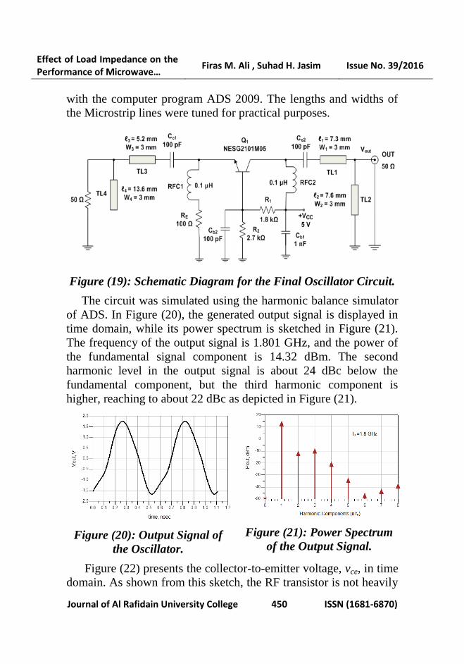
The schematic diagram of the final oscillator circuit is presented
in Figure (19). As shown from this figure, the transmission line
sections were implemented using Microstrip lines. The selected
Microstrip substrate type is the low cost epoxy-glass (FR-4) which
has a relative dielectric constant εr of 4.5 and thickness h = 1.6 mm.
The tangent loss of this substrate is about 0.01, while the conductor
thickness t = 0.05 mm. The ideal transmission line sections were
converted into Microstrip lines using the Linecalc tool provided
Effect of Load Impedance on the Performance of Microwave…
Firas M. Ali , Suhad H. Jasim Issue No. 39/2016
Journal of Al Rafidain University College 450 ISSN (1681-6870)
with the computer program ADS 2009. The lengths and widths of
the Microstrip lines were tuned for practical purposes.
Figure (19): Schematic Diagram for the Final Oscillator Circuit.
The circuit was simulated using the harmonic balance simulator
of ADS. In Figure (20), the generated output signal is displayed in
time domain, while its power spectrum is sketched in Figure (21).
The frequency of the output signal is 1.801 GHz, and the power of
the fundamental signal component is 14.32 dBm. The second
harmonic level in the output signal is about 24 dBc below the
fundamental component, but the third harmonic component is
higher, reaching to about 22 dBc as depicted in Figure (21).
Figure (20): Output Signal of
the Oscillator.
Figure (21): Power Spectrum
of the Output Signal.
Figure (22) presents the collector-to-emitter voltage, vce, in time
domain. As shown from this sketch, the RF transistor is not heavily

Effect of Load Impedance on the Performance of Microwave…
Firas M. Ali , Suhad H. Jasim Issue No. 39/2016
Journal of Al Rafidain University College 451 ISSN (1681-6870)
driven into saturation. In Figure (23), the phase noise of the
oscillator is sketched and is about -108 dBc/Hz at an offset
frequency of 100 kHz from the carrier.
Figure (22): Collector-to-
Emitter Voltage.
Figure (23): Simulated Phase
Noise of the Circuit.
6. Conclusion
The effect of load impedance on the performance
characteristics of negative resistance microwave oscillators has
been studied thoroughly in this paper. Analytic expressions have
been derived for the optimum load impedance in terms of the small
signal Z-parameters of the RF transistor. These relations are
convenient as an initial guess for the RF oscillator design prior to
computer optimization. Throughout computer simulation, it was
shown that the optimum load resistance and reactance are
dependent on each other. The optimum load impedance varies also
with the signal power level at which the active device is operating
with. Hence, the load and input impedances of the RF transistor
should be extracted at the specific power level for a successful
large-signal oscillator design. Furthermore, it was shown that the
optimum load impedance for maximum negative input resistance
does not coincide with its value required for maximum output
power. This difference usually extends as the signal level becomes

Effect of Load Impedance on the Performance of Microwave…
Firas M. Ali , Suhad H. Jasim Issue No. 39/2016
Journal of Al Rafidain University College 452 ISSN (1681-6870)
larger. The shift between the two values may probably change from
device to device.
A 1.8 GHz grounded-base oscillator circuit was designed
and simulated with the aid of the microwave CAD program ADS
2009 to confirm the approach of analysis. This circuit is based on a
SiGe HBT transistor and generates an RF signal at 1.8 GHz with an
output power level of more than 14 dBm, and produces a phase
noise of -108 dBc/Hz at an offset frequency of 100 kHz from the
frequency of oscillation.
References
[1] Alechno, S., “Analysis method characterizes microwave
oscillators," Microwaves & RF, Vol. 36, No. 11, pp. 82-86,
1997.
[2] Randall, M. and M. J. Hock, “General oscillator
characterization using linear open-loop S-parameters," IEEE
Transactions on Microwave Theory and Techniques, Vol.
49, No. 6, pp. 1094-1100, 2001.
[3] Kurokawa, K., “Some basic characteristics of broadband
negative resistance oscillator circuits”, Bell Systems
Technical Journal, Vol. 48, No. 6, pp. 1937-1955, 1969.
[4] Zhang, J., “A y-parameter approach to the design of one-port
negative resistance oscillators”, in Proceedings of the 2013
International Conference on Measurement, Information and
Control (ICMIC), Harbin, China, pp. 214-217, 2013.
[5] Rhea, R. W., Discrete Oscillator Design: Linear, Nonlinear,
Transient, and Noise Domains, Artech-House Publishers,
New York, 2010.
[6] R. Ludwig and G. Bogdanov, "RF Circuit Design: Theory
and Applications", 2nd
Edition, Pearson Educations, Upper
Saddle River, NJ, 2009.
[7] Kurokawa, K., Beccone, J. P., and Kenyon, N. D.,
“Broadband negative resistance oscillator circuits”, in

Effect of Load Impedance on the Performance of Microwave…
Firas M. Ali , Suhad H. Jasim Issue No. 39/2016
Journal of Al Rafidain University College 453 ISSN (1681-6870)
Proceedings of the 1969 G-MTT International Microwave
Symposium, pp. 281-284, 1969.
[8] Kotzebue, K. L. and Parrish, W. J., "The use of large signal
S-parameters in microwave oscillator design", in
Proceedings of the 1975 IEEE International Microwave
Symposium on Circuits and Systems, pp. 487-490, 1975.
[9] Mitsui, Y., Nakatani, M., and Mitsui, S., "Design of GaAs
MESFET oscillators using large signal S-parameters", IEEE
Transactions on Microwave Theory and Techniques, Vol.
25, pp. 981-984, 1977.
[10] Johnson, K. M. "Large signal GaAs MESFET
oscillator design", IEEE Transactions on Microwave Theory
and Techniques, Vol. 27, No. 3, pp. 217 -227, 1979.
[11] Gilmore, R. J. and Rosenbaum, F. J. "GaAs
MESFET oscillator design using large-signal S-
parameters", in Proceedings of the 1983 IEEE MTT-S
International Microwave Symposium Digest, pp. 279-281,
1983.
[12] Kotzebue, K.L. "A Technique for the Design of
Microwave Transistor Oscillators (Short Paper)", IEEE
Transactions on Microwave Theory and Techniques, Vol.
32, No. 7, pp. 719 - 721, 1984.
[13] Abe, H., "A GaAs MESFET oscillator quasi-linear
design method", IEEE Transactions on Microwave Theory
and Techniques, Vol. 34, No. 1, pp. 19 -25, 1986.
[14] Lam , V. M. T., Yip, P. C. L. and Poole, C. R.,
"Microwave oscillator design with power
prediction", Electronics Letters, Vol. 27, No. 17, pp. 1574
– 1575, 1991.
[15] Kormanyos, B. K. and Rebeiz, G. M., “Oscillator
design for maximum added power”, IEEE Microwave and
Guided Wave Letters, Vol. 4, No. 6, pp. 205 –207, 1994.
[16] Grebennikov, A. and Nikiforov, V., “An analytic
method for microwave transistor oscillator design”,
International Journal of Electronics, Vol. 83, No. 6, pp. 849-
858, 1997.

Effect of Load Impedance on the Performance of Microwave…
Firas M. Ali , Suhad H. Jasim Issue No. 39/2016
Journal of Al Rafidain University College 454 ISSN (1681-6870)
[17] Grebennikov, A., “Microwave transistor oscillators:
an analytic approach to simplify computer-aided design,”
Microwave Journal, Vol. 42, No. 5, pp. 292–300, 1999.
[18] Grebennikov, A., “Microwave FET oscillators: an
analytic approach to simplify computer-aided design,”
Microwave Journal, Vol. 43, No. 1, pp. 100–110, 2000.
[19] Ain, M. F., Lancaster, M. J., and Gardner, P., “Design
of L-band microwave oscillators”, in Proceedings of the
2001 6th IEEE High Frequency Postgraduate Student
Colloquium, Cardiff, UK, pp.19-24, September 2001.
[20] Zhan, J.-H. Conan, Maurice, K., Duster, J. and
Kornegay, K. V., "Analysis and design of negative
impedance LC oscillators using bipolar transistors", IEEE
Transactions on Circuits and Systems-I: Fundamental
Theory and Applications, Vol. 50, No. 11, pp. 1461-1464,
2003.
[21] Hsin, W. H. H., Chet, K. V., and Kung, F., “The
design and development of a 1.4 GHz VCO”, in Proceedings
of the 2005 Asia-Pacific Conference on Applied
Electromagnetics, Malaysia, December 2005.
[22] Suh, I. et al., “Negative input resistance and real-time
active load-pull measurements of a 2.5GHz oscillator using a
LSNA”, in Proceedings of the 2007 69th ARFTG
Conference, Honolulu, HI, pp. 1-6, June 2007.
[23] Chen, Y., Mouthaan, K., and Ooi, B-L., “A Novel
Technique to Enhance the Negative Resistance for Colpitts
Oscillators by Parasitic Cancellation”, in Proceedings of the
IEEE Conference on Electron Devices and Solid-State
Circuits, Tainan, pp. 425-428, December 2007.
[24] Suh, I., Roblin, P., Doo, S. J., Cui, X., Strahler, J.,
and Rojas, R. G. , "Measurement-based methodology to
design harmonic-loaded oscillators using real-time active
load pull", IET Microwaves, Antennas & Propagation, Vol.
5, No. 1, pp. 77-83, 2011.
[25] Pelaez-Perez, A. M., Woodington, S., Barciela , M.
F., Tasker, P. J., and J. I. Alonso, "Large signal oscillator

Effect of Load Impedance on the Performance of Microwave…
Firas M. Ali , Suhad H. Jasim Issue No. 39/2016
Journal of Al Rafidain University College 455 ISSN (1681-6870)
design procedure utilizing analytical X-parameters closed-
form expressions", IEEE Transactions on Microwave Theory
and Techniques, Vol. 60, No. 10, pp. 3126-3136, 2012.
[26] Barakat, A., Evaluation of an Existing Approach for
Oscillator Power Optimization, M.Sc. Thesis, Tampere
University of Technology, Finland, 2013.
[27] Zargar, H., and Banai, A., “A new stability criterion
for negative resistance oscillators based on X-parameters”,
in Proceedings of the 2015 23rd Iranian Conference on
Electrical Engineering, Tehran, Iran, pp. 231-234, May
2015.
[28] Grebennikov, A., RF and Microwave Power
Amplifier Design, McGraw-Hill, 2005.
[29] Gonzalez, G., Foundations of Oscillator Circuit
Design, Artech-House, Norwood, MA, 2007.
[30] Bahl, I. J., Fundamentals of RF and Microwave
Transistor Amplifiers, John Wiley & Sons, 2009.
[31] Niu, G. et al., “Noise-gain tradeoff in RF SiGe
HBTs”, Solid-State Electronics, Vol. 46, No. 9, pp. 1445-
1451, 2002.

Effect of Load Impedance on the Performance of Microwave…
Firas M. Ali , Suhad H. Jasim Issue No. 39/2016
Journal of Al Rafidain University College 456 ISSN (1681-6870)
تأثير ممانعة الحمل على أداء مذبذبات الموجات المايكروية ذات
المقاومة السالبة
م.م. فراس محمد علي[email protected]
قسم الهندسة الكهربائية -الجامعة التكنولوجية
سهاد حسين جاسم م.م[email protected]
قسم الهندسة الكهربائية -الجامعة التكنولوجية
:المستخلص
في مذبذبات الموجات المايكروية ذات المقاومة السالبة يكون الجزء الحقيقي لممانعة
وبالعودة إلى النظرية التقليدية لتحليل منفذ الدخل أو الخرج للترانزستور الراديوي سالبا.
ألجل تحقيق شرط التذبذب مع الحصول المذبذبات الراديوية ذات المقاومة السالبة فإنه
أو ة خرج من الدائرة فإن مقدار الجزء الحقيقي السالب لممانعة الدخل على أقصى قدر
الخرج يتم جعله أقصى ما يمكن.
يناقش هذا البحث تأثير ممانعة الحمل للدائرة على قيمة مقاومة الدخل السالبة
وخصائص أداء المذبذب األخرى. وقد تم اشتقاق معادالت جديدة الستخراج قيمة ممانعة
لدائرة المذبذب ذو القاعدة المشتركة بداللة معامالت الممانعة للترانزستور الحمل المثلى
الراديوي وذلك لتحقيق أعلى قيمة لمقاومة الدخل السالبة. باإلضافة إلى ذلك تم استخدام
برامج التصميم المعزز بالحاسوب الالخطية لتتبع التغير بقيمة ممانعة الحمل المثلى في
عة العالية عن قيمتها المحسوبة في حالة اإلشارات ذات السعة حالة اإلشارات ذات الس
الصغيرة.
وقد لوحظ بأن قيمة ممانعة الحمل المثلى الالزمة لتحقيق أعلى مقاومة دخل
سالبة تختلف ألى حد ما عن قيمتها الالزمة لتحقيق أقصى قدرة خرج من الدائرة في حالة
ومحاكاة دائرة مذبذب راديوي تعمل في اإلشارت ذات السعة العالية. وقد تم تصميم

Effect of Load Impedance on the Performance of Microwave…
Firas M. Ali , Suhad H. Jasim Issue No. 39/2016
Journal of Al Rafidain University College 457 ISSN (1681-6870)
ثنائي القطب ذو وباستخدام ترانزستور عالي المواصفات من النوع GHz 1.8التردد
لتأكيد طريقة التحليل. (SiGe HBT) الوصلة غير المتجانسة
: مذبذبات المقاومة السالبة، مذبذب القاعدة المشتركة، الدوائر رئيسيةالكلمات ال
ات ثنائية القطب ذات الوصلة غير المتجانسة.ترانزستورال الالخطية،المايكروية