
Effcet of Tunneling
8
IEEE TRANSACTIONS ON ELECTRON DEVICES, VOL. 39, NO. 2, FEBRUARY 1992 33 1 10-@ A New Recombination Model for Device Simulation Including Tunneling NA=~XIO’@ N~=10’@ , G . A . M . Hurkx, D . B. M . Klaassen, and M . P. G . Knuvers Abstract-A new recombination model for device simulation is presented. This model includes both trap-assisted tunneling under forward and reverse bias) and band-to-band tunneling Zener tunneling). The model is formulated in terms of analyt- ical functions of local variables which makes it easy to imple- ment in a numerical device simulator. The trap-assisted tun- neling effect is described by a n expression that f or weak electric fields reduces to the conventional Shockley-Read-Hall SRH) expression for recombination via traps. Compared to the con- ventional SRH expression, the proposed model has one extra physical parameter, vis. the effective mass m . or m = 0 25m0 the model correctly describes the experimental observations as- sociated with tunneling, including the distinctl y d ifferent tem- perature behavior of trap-assisted tunneling and band-to-band tunneling. The band-to-band tunneling contribution is found to be important at room temperature for electric fields larger than 7 X lo5 V/cm. It is shown that for dopant concentrations above 5 X 1 ” or, equivalently, for breakdown voltages below approximately 5 V, the reverse characteristics are dominated by band -to-band tunneling. 1. INTRODUCTION ECE NT developments in both bipolar and MOS tech- R ologies, such as lateral downscaling, shallow-junc- tion formation, and the use of self-alignment techniques, have led to an increase in electric field strength around p-n junctions in these devices. In bipolar transistors it is particularly the emitter-base junction at the emitter pe- riphery where the maximum electric field can reach values as high as lo6 V/cm, while in MOS transistors such strong fields can occur at the drain. In addition, the high intrinsic-base dopant concentration possible in Si/SiGe/Si heterojunction bipolar transistors also gives rise to strong electric fields at the intrinsic emitter-base junction. It is a well-known fact that in a strong electric field, tunneling of electrons through the bandgap can signifi- cantly contribute to carrier transport in a p-n junction [ 11, [2]. Both transitions directly from band to band (Zener tunneling) and transitions via traps (trap-assisted tunnel- ing) can be important. Tunneling not only adversely af- fects the leakage currents (e.g., the so-called “Zener breakdown”) but it can also lead to an anomalously high Manuscript received February 28, 1991. Part of this work was funded by ESPRIT Project 2016. The review of this paper was arranged by As- D. The authors are with Philips Research Laboratories, 56 00 JA Eindhoven, The Netherlands. IEEE Log Number 9104679. nonideal current under forward bias (forward-biased tun- neling) [2]-[ 4]. The latter is shown in Fig. 1 where the current at 0.3 V forward bias and at room temperature is plotted versus the zero-bias depletion layer width for lit- erature data and for our own measurements [3], [5]-[7]. Details of this figure are given in Section IV . Other char- acteristic features of this high nonideal forward current are a reduced temperature dependence and a high non- ideality factor [3], [4]. For CAD purposes it is of crucial importance that these effects are properly taken into account in a numerical de- vice simulator. Since these effects can basically be con- sidered as the generation or recombination of electron- hole pairs, they must be incorporated into the recombi- nation term in the electron and hole continuity equations. Existing models for trap-assisted tunneling [2], [3] give a semi-empirical relation between the current density and a certain exponential function of the applied voltage. These models, however, suffer from the following drawbacks: Since these models describe tunneling by means of a current density , they are only suitable fo r post-processing calculations and cannot be incorporated into the continu- ity equations. 0018-9383/92$03.00 O 1992 IEEE
Transcript of Effcet of Tunneling

8/16/2019 Effcet of Tunneling
http://slidepdf.com/reader/full/effcet-of-tunneling 1/8
IEEE TRANSACTIONS ON ELECTRON DEVICES, VOL. 39, NO.
2,
FEBRUARY 1992
33 1
10-@
A
New Recombination Model for Device Simulation
Including Tunneling
~ N A = ~ X I O ’ @ N~=10’@
,
G .
A . M. H ur kx,
D. B. M .
Klaassen, and
M.
P. G. Knuvers
Abstract-A new recombination model for device simulation
is presented. This model includes both trap-assisted tunneling
under forward and reverse bias) and band-to-band tunneling
Zener tunneling). The model is formulated in terms of analyt-
ical functions of local variables which makes it easy to imple-
ment in a numerical device simulator. The trap-assisted tun-
neling effect is described by a n expression that f or weak electric
fields reduces to the conventional Shockley-Read-Hall SRH)
expression for recombination via traps. Compared to the con-
ventional SRH expression, the proposed model has one extra
physical parameter, vis. the effective mass m . or
m =
0 25m0
the model correctly describes the experimental observations as-
sociated with tunneling, including the distinctly d ifferent tem-
perature behavior of trap-assisted tunneling and band-to-band
tunneling. The band-to-band tunneling contribution is found to
be important at room temperature fo r electric fields larger than
7 X lo5
V/c m. It is shown that for dopant concentrations above
5
X
1 ” or, equivalently, for breakdown voltages below
approximately 5 V, the reverse characteristics are dominated
by band -to-band tunneling.
1.
INTRODUCTION
ECE NT developments in both bipolar and MOS tech-
R ologies, such as lateral downscaling, shallow-junc-
tion formation, and the use of self-alignment techniques,
have led to an increase in electric field strength around
p-n junctions in these devices. In bipolar transistors it is
particularly the emitter-base junction at the emitter pe-
riphery where the maximum electric field can reach values
as
high as
lo6
V/cm, while in MOS transistors such
strong fields can occur at the drain. In add ition, the high
intrinsic-base dopant concentration possible in Si/SiG e/Si
heterojunction bipolar transistors also gives rise to strong
electric fields at the intrinsic emitter-base junctio n.
It is a well-known fact that in a strong electric field,
tunneling of electrons through the bandgap can signifi-
cantly contribute to carrier transport in a p-n junctio n [11,
[2]. Both transitions directly from band to band (Zener
tunneling) and transitions via traps (trap-assisted tunnel-
ing) can be important. Tunneling not only adversely af-
fects the leakage currents (e.g., the so-called “Zener
breakdown”) but it can also lead to an anomalously high
Manuscript received February 28, 1991. Part of this work was funded
by ESPRIT Project 2016. The review of this paper was arranged by
As-
sociate Editor D.D. ang.
The authors are with Philips Research Laboratories, 56 00 JA Eindhoven,
The Netherlands.
IEEE Log Number 9104679.
nonideal current under forward bias (forward-biased tun-
neling) [2]-[4]. The latter is shown in Fig.
1
where the
current at 0.3 V forward bias and at room temperature is
plotted versus the zero-bias depletion layer width fo r lit-
erature data and for our own measurements [3], [5]-[7].
Details of this figure are given in Section IV . O ther char-
acteristic features of this high nonideal forward current
are a reduced temperature dependence and a high non-
ideality factor [3],
[4].
For C AD purposes it is of crucial importance that these
effects are properly taken into account in a num erical de-
vice simulator. Since these effects can basically be con-
sidered as the generation or recombination of electron-
hole pairs, they must be incorporated into the recombi-
nation term in the electron and hole continuity equations.
Existing models for trap-assisted tunneling [2], [3] give a
semi-empirical relation between the current density and a
certain exponential function of the applied voltage. T hese
models, however, suffer from the following drawbacks:
Since these models describe tunneling by means of a
current density , they are only suitable fo r post-processing
calculations and cannot be incorporated into the continu-
ity equations.
0018-9383/92$03.00 O 1992 IEEE
8/16/2019 Effcet of Tunneling
http://slidepdf.com/reader/full/effcet-of-tunneling 2/8
332
IEEE TRANSACTIONS ON ELECTRON DEVICES, VOL. 39, NO. 2, FEBRUARY 1992
They only describe the voltage dependence of the
current density, while its magnitude must be obtained
from experiments.
The predicted temperature dependence is too weak
In this paper we present a recombination model which
takes into account band-to-band tunneling in reverse-bias
and trap-assisted tunneling in both forward and reverse
bias. In situations of a weak electric field (i.e ., lowly
doped junctions) the model reduces to the conventional
Shockley-Read-Hall expression for recombination via
traps. In
[4], [SI
we have established the basic physics
behind the model. In this work we concentrate on the for-
mulation of the model for device simulation purposes and
on the comparison of simulation results with experiments.
In our model the total net recombination rate is given
[41.
by
where
Rtrap
s the contribution of transitions via traps (in-
cluding the conventional SRH recombination mechanism)
and Rbb, s the band-to-band tunn eling contribution. In the
following sections we discuss these two terms
in
detail,
while in Section IV a comparison is made between sim-
ulation results and experiments.
11. MOD ELING RAP-ASSIST EDU N N E L I N G
The net recombination rate via traps is determined by
the density of carriers captured per unit of time and the
probability per unit
of
time of emitting a free carrier from
a trap. To obtain an expression for
Rtrap
we start with the
following general phenomenological expression for the net
recombination rate resulting from a dynamic balance be-
tween the net rate of captured electrons and that of holes.
This expression reads (see, e.g.,
[9])
where
NT
is the trap density, while
n,
and
p t
are the den-
sities of electrons and holes which have the capture rates
c
and
c p ,
respectively. The quantities
e,l
and
ep
are the
respective probabilities per unit of time for the emission
of an electron or a hole . Both the density of captured car-
riers and the emission probability per unit of time are in-
creased by tunneling.
In a weak electric field the carrier densities at a certain
location in a depletion lay er are given by the conventional
density of free carriers in the conduction and valence
bands. However, in a strong electric field the density of
carriers at a certain location within the depletion layer in-
creased due to the finite probability of carriers tunneling
into the gap. For instance an electron at location
x l
in Fig.
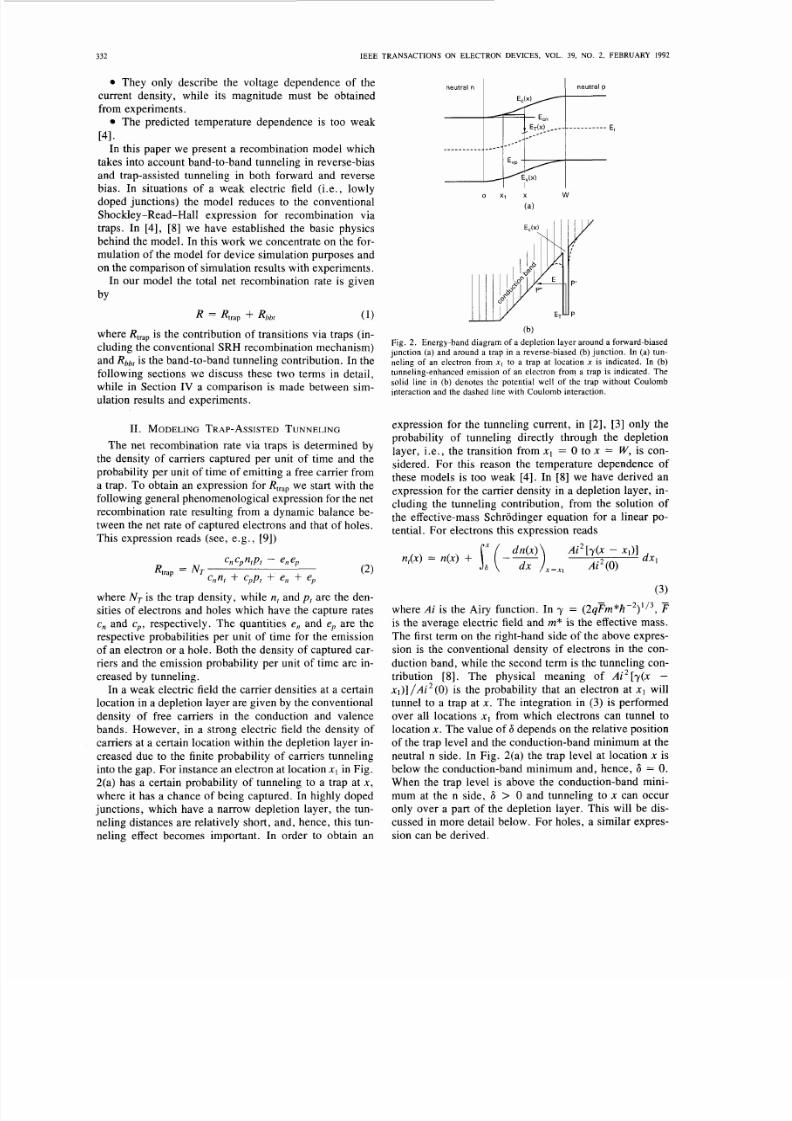
2(a) has a certain probability of tunneling to a trap at
x ,
where it has a chance of being captured. In highly doped
junctions, which have a narrow depletion layer, the tun-
neling distances are relatively short, an d, henc e, this tun-
neling effect becomes important. In order to obtain an
neut ra l
n
neut ra l p
1
b)
Fig.
2.
Energy-band diagram of a depletion layer around a forward-biased
junction (a) and around a trap in a reverse-biased (b) junction. In (a) tun-
neling of an electron from
x ,
to a trap at location x is indicated. In (b)
tunneling-enhanced emission of an electron from a trap is indicated. The
solid line
in
(b) denotes the potential well of the trap without Coulomb
interaction and the dashed line with Coulomb interaction.
expression for the tunneling current, in
[2], [3]
only the
probability of tunneling directly through the depletion
layer, i.e., the transition from
x 1 =
0 to x
=
W , is con-
sidered. For this reason the temperature dependence of
these models is too weak [4]. In [SI we have derived an
expression for the carrier density in a depletion layer, in-
cluding the tunneling contribution, from the solution of
the effective-mass Schrodinger equation for a linear po-
tential. For electrons this expression reads
3)
where
Ai
is the Airy function. In
y = 2qFm*h-2)”3, F
is the average electric field and
m*
is the effective ma ss.
The first term on the right-hand sid e of the above expres-
sion is the conventional density of electrons in the con-
duction band, while the second term is the tunneling con-
tribution [SI. The physical meaning of
Ai2[y x
x l ) ] A i 2
(0) is the probability that an electron at
x 1
will
tunnel to a trap at
x .
The integration in
3)
is performed
over all locations
x 1
from which electrons can tunnel to
location
x .
The value of
6
depends on the relative position
of the trap level and the conduction-band minim um at the
neutral n side. In Fig. 2(a) the trap level at location x is
below the conduction-band minimum and, hence,
6 = 0.
When the trap level is above the conduction-band mini-
mum at the n side,
6
> 0 and tunneling to x can occur
only over a part of the depletion layer. This will be dis-
cussed in more detail below. For holes, a similar expres-
sion can be derived.
8/16/2019 Effcet of Tunneling
http://slidepdf.com/reader/full/effcet-of-tunneling 3/8
HURKX er a l . : A NEW MODEL FOR DEVICE SIMULATION INCLUDING TUNNELING 333
The emission of electrons and holes from a trap is en-
hanced by the phonon-assisted tunneling effect (see Fig.
2(b)) [ lo], [4]. Instead of thermal emission ov er the entire
trap depth
E, ET,
which is the only escape mechanism
possible in the absence of a field, carriers can also be
emitted by thermal excitation over only a part of the trap
depth (transition P P‘ in Fig. 2(b)), followed by tun-
neling through the remaining potential barrier (transition
P ’ P ”).
Following the approach of Vincent
et al .
[ l o ] ,
the expression for the enhancement of the emission p rob-
ability is given by an integral over the trap depth of the
product of a Boltzmann fa ctor, which gives the excitation
probability of a carrier at the trap level to an excited level
E , and the tunneling probability at that energy level from
the trap to the band. F or electrons the emission probabil-
ity reads
e Ai
(0) d E
i 2 ( 2 m * y - 2 h - 2 E )
(4)
where
e,,Os
the emission probability in the absence of an
electric field. Again, the value of A E,,
depends on the rel-
ative position of the trap level and the conduction-band
minimum at the neutral n side. F or the situation sketched
in
Fig. 2(b), tunneling at all levels between
ET
and
E ,
is
possible,
so A E , = E, ET.
In order to make
(3)
and
(4)
suitable for implementation
into a numerical device simulator, we must express these
tunneling effects in terms of analytical functions which
depend on local variables only. For a linear potential it
can be shown that both the carrier concentration and the
emission probability are enhanced by the same factor, i.e .
( 5 4
(5b)
n ? =
r,,+ 1
en0 n
p - p t = r p + i
e p o P
where we have introduced the field-effect functions rn nd
rp .
ollowing the sam e derivation used to obtain the con-
ventional SRH expression from
( 2 )
[9], we arrive at
where
The quantity F is the local electric field. Analytical ap-
proximations for the integral in
(7)
are given in the Ap-
pendix.
Because the conduction-band minimum
E&)
and the
valence-band maximum
E&)
are a function of the posi-
tion in the depletion layer, the absolute value of the trap
level
ET(x)
is also position-dependent. This implies that
also the integration intervals A E,(x) and A Ep(x )are po-
sition-dependent. For the determination of these integra-
tion intervals we must distinguish between two situations:
For the situation of a trap at location x in Fig. 2(a), which
is important in forward-biased junctions, tunneling can
occur only at an energy level between the local conduc-
tion-band minimum
E,(x)
and the conduction-band mini-
mum at the neutral n side E,,, because below E,, there are
no states available from (and into) which an electron can
tunnel. In the case where the trap level
Ej-(x)
lies above
E,, (most important in reverse bias, see Fig. 2(b)) the in-
tegration interval is the whole trap depth, i.e.
,
A E,(x)
=
E,(x) ET(x).
For holes, a similar criterion holds. The
expression for the integration intervals can be written as
AEn(x) = Ern, ET@)5 Ern
= E&) ET@ ) , ET(x ) > Ern
(9a)
and
AEp(x)
= Evp Ev x17
ET(x) > Evp
= ET(x) 5 Evp. (gb)
For device simulation the quantities
E&) , E&) ,
and
ET(x) can easily be determined from the electrostatic po-
tential ( i. e. , the isri ns ic Ferm i level) , the local value of
the bandgap and E , which is the relative position of the
trap level with respect to the intrinsic Ferm i level. At high
dopant concentrations the Fermi level in a neutral region
nearly coincides with the corresponding band edge. For
this reason and because under low and medium fonvard-
where
E = ET Ei ,
i.e., the difference between the trap
level and the intrinsic level. The quantities
r,
and
rp
are
the recombination lifetimes of electrons and holes, re-
spectively, while
nie
is the intrinsic carrier concentration.
For weak electric fields,
rn ,p
<
1
and
6)
reduces to the
conventional
SRH
recombination formula.
Using the asymptotic behavior of the Airy function
Ai(y)
-
exp (-(2/3)y3I2), the expressions for
r,
and
r,
can be written as
bias conditions, where tunneling is important, the quasi-
Fermi levels are approximately constant in the depletion
region,
E,, and Eup can be replaced by
-q+ ,(x)
and
- q (x), respectively. The quantities +,(x) and +p x) are
the local quasi-Fermi levels of electrons and ho les. In re-
verse bias these levels are not constant but their relative
position with respect to the trap level is such that they do
provide the co rrect criterion for the integration intervals.
Using the analytical approximations for the integral in
(7),
together with 8) and (9),
6)
is readily suitable for
incorporation into a numerical device simulator. How-
8/16/2019 Effcet of Tunneling
http://slidepdf.com/reader/full/effcet-of-tunneling 4/8
334 IEEE TRANSACTIONS ON ELECTRON
DEVICES, VOL.
39, NO. 2. FEBRUARY 1992
ever, considering the validity of 6), together with (7),
two questions may arise.
The first one concerns the Poole-Frenkel effect, which
is the mechanism whereby in the case of Coulomb inter-
action between the free carrier and the trap, the effective
trap depth is lowered (s ee dashed line in Fig . 2 (b) ). This
is not taken into account in the above expressions. At a
strong electric field this effect is much weaker than the
tunneling effect, but at a weak field it can greatly enhance
the emission probability [l o] . This Poole-Frenkel effect
occurs in processes where the trap is neutral when it is
occupied by a carrier (either a hole or an electron) and
charged when the carrier is being emitted. However, since
a trap is either donor- o r acceptor-like only o ne of the two
field-enhancement factors in
(6)
increases due to the
Poole-Frenkel effect [9]. The maximum influence of t he
Poole-Frenkel effect on
Rtrap
ccurs when one of the two
field-enhancement factors in (6)becomes so large that Rtrap
is determined solely by the slowest process, i.e ., the other
term in the denominator. That term only experiences the
tunneling effect. Th is implies that the overall influence of
the Poole-Frenkel effect on the net recombination rate is
fairly limited (maximum a factor of 2 for midgap states
and equal lifetimes for electrons and holes).
The second question which may arise concerns the va-
lidity of using a linear potential to calculate the tunneling
probability. This can be investigated by replacing the tun-
neling probability evaluated for a constant field
Ai2
y(x
x l ) ] A i 2 0) (or its asymptotic approximation in (7)) by
the WKB expression [111
Tt = exp / -2
i: IK(X )I
d x ' j
(10)
which is valid for an arbitrary potential. In (lo),
I K ( x ) (
is the absolute value of the wave vector of t he carrier in
the gap, which is determined by the actual potential dis-
tribution between xI, nd
x .
Fig. 3 shows the numerically
calculated value of r or a trap in the middle of a for-
ward-biased, linearly graded junction versus the depletion
layer width (i .e., the doping gradient) for three cases:
1) the tunneling probability evaluated for a constant
field is used and for F the local electric field at the
trap is taken (dotted line);
2) the tunneling probability evaluated for a constant
field is used and for
F
the average electric field in
the depletion layer is taken (dashed line);
3) the tunneling probability as given by (10) is used
(solid line).
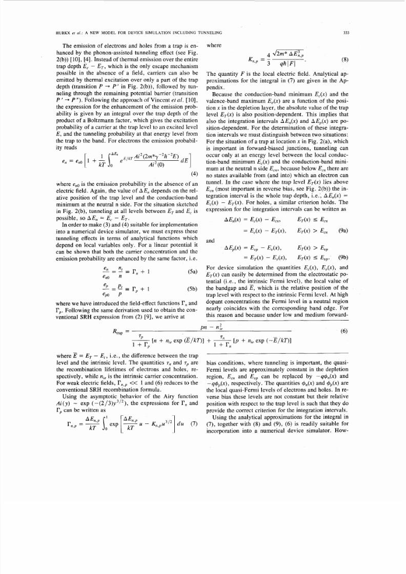
From Fig. 3 we observe that the choice of the local elec-
tric field gives results which agree better with the WKB
calculations than the results obtained with the average
field. At this point is should be noted that both (7) and
(lo), as well as the expression of Vincent t al. [ lo ] ac-
counting for the Poole-Frenkel effect, are obtained in a
one-dimensional (1D) approach. A three-dimensional
(3D) numerical treatment of these problems show that a
t
c
c
1014
1012
10'0
108
106
1
o4
102
0 200
400 600
800 1000
depletion width A )
-
Fig.
3 .
The field-effect function
I
in the case
of A E , , = 0.4 e V
versus
the depletion-layer width of a forward-biased , linearly graded junction
for
two temperatures. The solid lines are obtained
by
using (10) for the tun-
neling prob ability, while the other lines a re obtained by using the tunneling
probability for a constant electric field (dashed lines: average field; dotted
lines: local field).
small variation of the effective mass in the 1D expressions
can account for the 3D effects. T o account for the above-
mentioned effects, the value of the effective mass to be
used in
(8)
is obtained from a comparison of simulations
with experiments. Using the local value of the electric
field in 8) , the experimentally obtained value of m* is
0.25mo (see Section IV and F ig. 7), which is quite a plau-
sible one.
111. MOD ELIN G AND -TO-B ANDUNNELING
For the band-to-band tunneling contribution Rbbrwe
base ourselves on the theoretical work of Keldysh and
Kane [121-[ 141. Since silicon is an indirect semiconduc-
tor whose direct bandgap is much larger than its indirect
gap, indirect transitions including electron-phonon inter-
action are predominant. Keldysh calculated the transition
rate on the basis of a solution of the time-dependent
Schrodinger equation , including electron-phonon inter-
action. His results were later adopted by Kane to obtain
an expression for the tunneling current density per unit of
energy d J b b r / d E [14]. Both directly from the work of
Keldysh, and from Kane's work by using the relation
the following expression for Rbbtcan be obtained:
In [12]-[14] it can be found that U = 2 for direct transi-
tions and
U
= 5 / 2 for indirect transitions, including elec-
tron-phonon interaction. Since silicon is an indirect semi-
conductor, we use
U
= 5/ 2. In (1 1) rl, is the electrostatic
potential, while in (12) E and E are the Fermi levels at
the neutral n and p side, respectively. In the above trans-
formation from d Jbbt o Rbbrhe tunneling of an electron
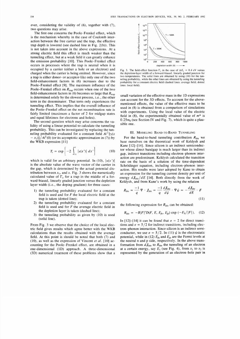
at a certain energy, say E l (see Fig. 4), from x 1 to
x
is
represented by the generation of an electron-hole pair in
8/16/2019 Effcet of Tunneling
http://slidepdf.com/reader/full/effcet-of-tunneling 5/8
HURKX er
a l . :
A NE W M ODE L
FOR
DE VI CE S I M UL AT I ON I NCL UDI NG T UNNE L I NG
335
neut ra l p
. - - - - - - - - -
neut ra l
n
4
t
A
_ _ _ _ _ _ - - -
x xp x
Fig. 4 . Schematic energy-band diagram
of
a reverse-biased
p-n
junc t ion.
The band-to-band tunneling mechanism is indicated. Band-to-band tunnel-
ing is only possible in the region x,,
5
x
<
x
the middle of the gap xI + x2 ) /2 . The function D ( F , E ,
Eb,, ESP)
accounts for the relative position of the Fermi
levels
Efi,
and Efp in the neutral regions and for the influ-
ence of the motion of the electron perpendicular to the
electric field
on
the tunneling probability
[
141. In forward
bias, it accounts for the well-known peak in the tunneling
current observed in Esaki diodes. An expression for
D ( F ,
E , Eb,,
Eh),
which is valid in zero and reverse bias and
which is suitable for implementation in a device simulator
can be obtained from [14]. This gives
(13)
1
exp [(-E, q$) /kTl + 1 .
This function virtually equals zero for
< x,
in Fig. 4,
because in this region there are no final states into which
an electron can tunnel. Fo rx
>
xp n Fig. 4, this function
also equals zero because there are no initial states from
which electrons can tunnel. For
x, < <
xp
or, equiva-
lently, when the tunneling energy El lies between
Ef,
nd
ESP,
his function equals unity.
As
in the case of trap-as-
sisted tunneling, the quantities
Efi,
nd
Eh
can be replaced
by
-q (x)
and -q4p(x), respectively. However, from
numerical simulations it is found that when the current
density in reverse bias is very high, the above replace-
ment gives incorrect results. Th e reason fo r this is that the
finite saturated drift velocity of the carriers causes a n in-
crease in the ca me r densities. When the generated elec-
tron and hole densities are in the order of the intrinsic
carrier density, the quasi-Fermi levels lie very close to the
intrinsic level
E, (E , =
-q$ ). In that case, the replace-
ment of
Ef,
and
Eh
by -q&(x) and
-q p
x)
ives a value
of
D
significantly less than its actual value 1. This can be
remedied simply by putting
D
=
1 at those mesh points
where the magnitude of the electron or hole current den-
sity has increased to a certain fraction (e.g . , l o p3 ) of
qnrcUs,where
U ,
is the saturated drift velocity.
The quantities F, and B at room temperature are found
to be 1.9
X
lo7 V /cm and 4
X
l O I 4
c m - ' l 2
*
V p 5 / *
s - ' ,
respectively [4], [15]. The prefactor
B
is taken to be
temperature-independent. Th e quantity F,, which is pro-
portional to
where
Eg
is the bandgap [12]-[14], de-
pends on the temperature due to the temperature depen-
dence of this bandgap. In order to have an idea of the
electric field strength above which band-to-band tunnel-
ing becomes important at room temperature, we compare
Rbbt
with the ratio
n r e / r ,
which is a measure of the gen-
eration rate via traps. When we take for this ratio a real-
istic value (at room temperature) of
IO"
c m P 3
*
s- ' , we
find that band-to-band tunneling becomes important at a
field strength above 7
X lo5
V / c m .
IV. SIMULATIONESULTS
N D A
COMPARISONITH
EXPERIMENTS
To give an impression of the model behavior, Fig.
5
shows
1D
simulations of diodes in reverse and forward
bias. T he diodes are step junctions with
No = lo2'
c m p 3 ,
while
N A
is varied. In these simulations conventional
models for the mobilities, bandgap n arrowing, recomb i-
nation lifetimes, and impact-ionization rates are used, as
can be found, for instance, in [16]. Furthermore, we have
used E&)
=
E, x) (i. e., "midgap" states) and temper-
ature-independent lifetimes. From the reverse character-
istics, shown in Fig. 5(a), we can observe that for dopant
concentrations above
5
X lOI7 cmP3 or, equivalently, for
breakdown voltages below 4Eg/q-6Eg/q, the reverse
characteristics are dominated by band-to-band tunneling
(Zene r tunneling). This is in agreement with the criteria
mentioned in standard textbooks (e.g. , [17]). From the
forward characteristics given in Fig. 5(b) we see that the
nonideal current increases significantly for dopant con-
centrations above a few times 10' ' cm p3 , which is due to
trap-assisted tunneling. This is in agreement with exper-
imental observations in [3], [5]-[7] and with our own ex-
periments, as will be shown below.
Fig. 6 shows a comparison of simulation results with
measurements
on
different diodes having linearly graded
junctions. These diodes have a large junction area (204
x
204 pm2), and sidewall effects are eliminated by the
use of guard rings. T he junc tion is formed by the diffusion
of boron into a heavily doped, homogeneous n-type sub-
strate. The doping profiles are determined from
C-
I/mea-
surements and from the resistivity of the substrate. Diodes
A , B , and
C
have a zero-bias depletjon layer width of ap-
proximately 200, 270, and 400
A
respectively. The
magnitude of the calculated curves depends on the life-
times, while both the slope (i.e., the nonideality factor)
and the temperature depen dence are given by the effective
mass
m .
ince the values of the lifetimes are unknown,
we have taken a constant value for T,
=
r,, =
T
for each
diode. Fo r each diode the value of
T
is chosen such that
at T
=
294
K
the magnitude of the simulated curve, using
the new model, fits the measurements. The resulting life-
times are 0.6, 2.5, and 20
ps
for diodes
A , B ,
and
C ,
which have a substrate doping concentration of around 2
X
1019, 7
X lo1',
and 1.9
x
10" ~ m - ~ ,espectively.
8/16/2019 Effcet of Tunneling
http://slidepdf.com/reader/full/effcet-of-tunneling 6/8
336
IEEE TRANSACTIONS
ON
ELECTRON DEVICES. VOL. 39, NO. 2 . FEBRUARY 1992
0.0
5
10
15
reverse vo l tage (VI-
(a)
0.0 0.2 0.4 0 6 0.8
f o rw a rd vo l t a ge ( V I-
(b)
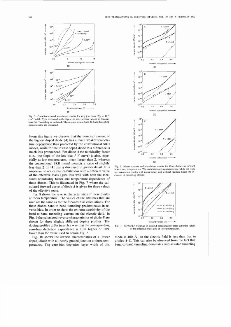
Fig.
5 .
One-dimensional simulation results for step junctions (N,] = IO”’
cm-3 while N A s indicated in the figure) in reverse bias (a ) and in forward
bias (b). Tunneling is includ ed. The regions where band-to-band tunneling
predominates are indicated.
From this figure we observe that the nonideal current of
the highest doped diode ( A ) has a much weaker tempera-
ture dependence than predicted by the conventional SRH
model, while for the lowest doped diode this difference is
much less pronounced. For diode A the nonideality factor
(i.e. , the slope
of
the low-bias
I-V
curve) is also, espe-
cially at low temperatures, much larger than
2 ,
whereas
the conventional
SRH
model predicts a value of slightly
less than
2.
In
[ ]
his is discussed in greater detail. It is
important to notice that calculations with a different value
of the effective mass agree less well with both the mea-
sured nonideality factor and temperature dependence of
these diodes. This is illustrated in Fig.
7
where the cal-
culated forward curve of diode A is given fo r three values
of the effective mass.
Fig.
8
shows the reverse characteristics of these diodes
at room temperature. The values of the lifetimes that are
used are the same as for the forward-bias calculations. For
these diodes band-to-band tunneling predominates in re-
verse bias. In order to show the ext reme sensitivity of the
band-to-band tunneling current on the electric field,
in
Fig.
9
the calculated reverse characteristics of diode
B
are
shown for three slightly different doping profiles. The
doping profiles differ in such a way that the corresponding
zero-bias depletion capacitance is
10%
higher or 10%
lower than the value used to obtain Fig. 8.
Fig. 10 shows the reverse characteristics of a (lower
doped) diod e with a linearly graded junction at three tem-
peratures. The zero-bias depletion layer width
of
this
c
? 10’0
10-12
, ,
0.0 0.2 0.4 0.6
f orward vo l tage (V)
-
(a)
I
1O ~ ’ 2
0.0
0 2
0.4
0 6
f orward vo l tage
(V)
-
(b)
0.0
0.2
0.4 0.6
f orward vo l tage (V)-
(C)
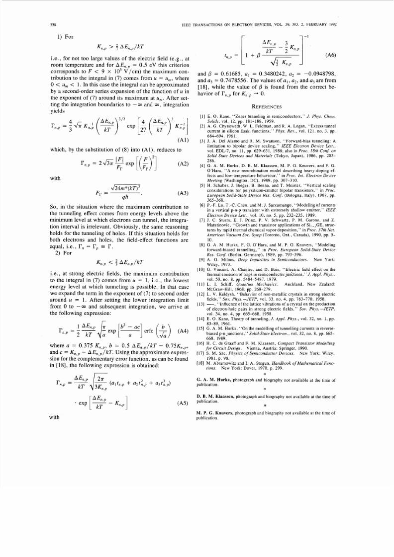
Fig.
6 .
Measurements and simulation results for three diodes in forward
bias at two temperatures. The solid dots are measurements, while the lines
are simulation results with (solid lines) and without (dashed lines) the in-
clusion
of
tunneling effects.
0.0 0 2 0.4 0.6
forward vo l tage
(V)
-
Fig. 7. Forward J-Vcu rves of diode
A
calculated for three different values
of the effective mass and at two temperatures.
diode is
460 A
so the electric field is less than that in
diodes A - C . This can also be observed from the fact that
band-to-band tunneling dominates trap-assisted tunneling

8/16/2019 Effcet of Tunneling
http://slidepdf.com/reader/full/effcet-of-tunneling 7/8
HURKX CI al . :
A
NE W M ODE L FOR DE VI CE S I M UL AT I ON I NCL UDI NG T UNNE L I NG
~
337
102
100
NI
10-2
i
3 1 0 ~ 4
?
10-6
1 0 8
t
U
1 8 8 1 1 1
0 1 2 3 4 5
reverse vol tage
(V)
-
Fig.
8.
Measurements (dots) and simulation results with (solid lines) and
without (dashed lines) tunneling for the three diodes
of
Fig.
6
in reverse
bias and at room temperature.
10
lo
I
I
0 1 2 3 4 5
reverse vol tage (V)-
Fig.
9.
Measurements and simulation results for diode
B
in reverse bias
for three slightly different doping profiles. The solid dots are measure-
ments. The solid line denotes the same simulation results as given in Fig.
8. The doping profiles corresponding to the dashed lines differ in such a
way that the corresponding zero-bias depletion capacitance is
10
higher
or 10% ower than the value used to obtain the curve in Fig.
8 .
E
t
m
E
2
YI
U
a
3
l o o t 1 : T = 2 9 4 K
2: T
=
338K
10
2
1 0 . ~
10-6
10-8
rn 10
3 : T = 3 8 3 K I
0 1 2 3 4 5 6
reverse vol tage (V)
-
Fig. 10. Reverse characteristics of
a
diode with a linearly graded junction
at three temperatures. The dots are measurements, while the lines
are
sim-
ulation results with (solid lines) and without (d ashed lines) tunneling. Fo r
this diode impact ionization is not included.
only above 3 V reverse bias. Notice the different temper-
ature dependence of the two regimes.
Finally, we return to Fig. 1,which shows a comparison
between measurements (from [3], [5]-[7] and own mea-
surements) and simulations. In this plot the forward cur-
rent density at
0.3
V and at room temperature is plotted
versus the zero-bias depletion width. For the data in [3]
and for our own data the values of the zero-bias depletion
layer width are obtained from the zero-bias depletion ca-
pacitance. For the other data we have estimated the de-
pletion lay er width from simulations on junctions with a
similar doping profile. Furthermore, although the junc-
tion areas are rather large, it is not explicitly mentioned
in [5]-[7] that sidewall effects do not play a significant
role. This means that, since the current density is obtained
by dividing the current by the junction area, for these data
the values of the current density are somewhat uncertain.
Neverthe lessb we can clearly observe that below approx-
imately
300
A
zero-bias depletion layer width or, equiv-
alently, above a dopant concentration of a few times lo'*
cm P3 for a steep junction, the nonideal current increases
significantly due to tunneling. When tunne ling is included
in the recombination model, this increase is also given by
the simulation results. In Fig. 1 this is shown by solid line
1 which represents results for a step function (similar to
the results in Fig . 5(b)) and by solid line 2 which are re-
sults for an emitter-base profile of a high-frequency pro-
cess. The dashed line is obtained for step junctions by
using the conventional recombination model without tun-
neling.
V . S U M M A R YND CONCLUSIONS
In this paper we have presented a new recombination
model for device simulation which includes both trap-as-
sisted tunneling and band-to-band tunneling (Zener tun-
neling). The model is formulated in terms of analytical
functions of local variables, which makes it easy to im-
plement in a numerical device simulator. The trap-as-
sisted tunneling effect is described by an expression that
for weak electric fields reduces to the conventional SRH
expression for recombination via traps. Compared with
the conventional SRH expression, the proposed model has
one extra physical parameter, viz. the effective mass m*.
For m* = 0.25mo, which is a quite plausible value, the
model correctly describes the following experimental ob-
servations:
1) The weak temperature dependence of the nonideal
forward current in heavily doped junctions.
2) The nonideality factor of such a junction which, es-
pecially at low temperatures, has a value significantly
larger than tw o.
3)
The significant increase in the nonideal current for
a diode wit a zero-bias depletion layer width less than
about 300
A ,
or, equivalently, above a dopant concen-
tration of a few times 10'' ~ 1 1 1 ~ ~
The band-to-band tunneling contribution is found to be
important at room temperature for electric fields larger
than 7 x lo5V/ cm . We have seen that for dopant con-
centrations above 5 X 10'' cm P3 or, equivalently, for
breakdown voltages below
4Eg
q - 6 E g
q
the reverse
characteristics are dominated by band-to-band tunneling.
This is in agreement with the criteria given in standard
textbooks.
APPENDIX
In order to obtain an analytical approximation for the
we must distinguish between
ield-effect functions
two situations:
8/16/2019 Effcet of Tunneling
http://slidepdf.com/reader/full/effcet-of-tunneling 8/8
IEEE TRANSACTIONS ON ELECTRON DEVICES, VOL. 39, NO. 2, FEBRUARY 199238
1) For
i.e., for not too large values of the electric field (e.g., at
room temperature and for A E n , p= 0.5 eV this criterion
corresponds to F < 9 X lo5V/cm) the maximum con-
tribution to the integral in (7) comes from U = U where
0
< U, < 1. In this case the integral can be approxim ated
by a second-order series expansion of the function of
U
in
the exponent of (7) around its maximum at
U .
After set-
ting the integration boundaries to - O and a ntegration
yields
which, by the substitution of (8) into (Al), reduces to
with
(‘43)
JiiGji
Fr
=
9h
So, in the situation where the maximum contribution to
the tunneling effect comes from energy levels above the
minimum level at which electrons can tunnel, the integra-
tion interval is irrelevant. Obviously, the same reasoning
holds for the tunneling of holes. If this situation holds for
both electrons and holes, the field-effect functions are
equal, i .e . , r, = rp= I’.
2) For
i.e., at strong electric fields, the maximum contribution
to the integral in (7) comes from
U
=
1, i .e . , the lowest
energy level at which tunneling is possible. In that case
we expand the term in the exponent of (7) to second order
around U = 1. After setting the lower integration limit
from
0
to --03 and subsequent integration, we arrive at
the following expression:
where a = 0.375 Kn,p,b = 0.5
AE,, , /kT
0.75Kn,,,
and c = Kn,p AE,,,/kT. Using the approximate expres-
sion for the complementary erro r function, as can be found
in [18], the following expression is obtained:
r 1 1
P
and p = 0.61685,
a l
= 0.3480242,
a2
= -0.0948798,
and u3 = 0.74785 56. Th e values of
a l ,
u 2 ,and u3are from
[18], while the value of p is found from the correct be-
havior of for K n , p
0.
REFERENCES
[ l ]
E. 0
Kane,
‘ ‘Zener
tunneling in semiconductors,”
J
Phys. Chem.
Solids,
vol. 12, pp. 181-188, 1959.
[2] A. G. Chynoweth, W. L. F eldman, and R. A. Logan, “E xcess tunnel
current in silicon Esaki functions,”
Phys. Rev.,
vol. 121,
no.
3, pp .
[3] J . A. Del Alamo and R. M. Swanson, “Forward-bias tunneling: A
limitation to bipolar device scaling,”
IEEE Electron Device Lett..
vol. EDL-7,
no.
11, pp. 629-631, 1986; also in
Proc. 18th Con
on
Solid Stare Devices and Materials
(Tokyo, Japan), 1986, pp. 283-
286.
[4] G. A. M. Hurkx, D. B. M. Klaassen, M. P. G Knuvers, and F. G.
O’Hara, “A new recombination model describing heavy-doping ef-
fects and low-temperature behaviour,” in
Proc. Int. Electron Device
Meeting
(Washington, DC), 1989, pp. 307-310.
[ 5 ]
H.
Schaber, J . Bieger, B. Benna, and T . Me ister, “Vertical scaling
considerations for polysilicon-emitter bipolar transistors,” in
Proc.
European Solid-State Device Res. Conf.
(Bologna, Italy), 1987, pp.
[6] P.-F. Lu, T.-C . Chen, and M. J. Saccamango, “Modeling
of
currents
in a vertical p-n-p transistor with extremely shallow emitter,”
IEEE
Electron Device L ett .,
vol. 10,
no.
5 ,
pp. 232-235, 1989.
[7] J . C . Sturm, E.
J .
Prinz, P. V. Schwartz,
P.
M. Garone, and Z.
Matutinovic, “Growth and transistor applications of Si, - GE, struc-
tures by rapid thermal chemical vapor depos ition,” in
Proc. 37th Nar.
American Vacuum Soc. Symp
(Toronto, On t., Canada), 1990, pp.
5 -
10.
[8] G. A.
M .
Hurkx, F .
G .
O’Hara, and
M .
P. G . Knuvers, “M odeling
forward-biased tunnelling,” in
Proc. European Solid-State Device
Res. Conf.
(Berl in, Germany), 1989, pp. 793-396.
[9] A. G. Milnes,
Deep Impurities in Semiconductors.
New York:
Wiley, 1973.
[lo ] G. Vincent, A. C hantre , and D. Bois, “Electric field effect
on
the
thermal emission of traps in semiconductor unktions,” J. Appl.
Phys.,
vol.
50 , no. 8 ,
pp. 5484-5487, 1979.
[ l l ] L . I . Schiff,
Quantum Mechanics.
Auckland, New Zealand:
McGraw-Hill , 1968, pp. 268-279.
[12]
L .
V. Keldysh, “Behavior of non-metallic crystals in strong electric
fields,”
Sov. Phys.-JETP,
vol. 33,
no.
4, pp. 763-770, 1958.
[13]
-,
“Influence
of
the lattice vibrations of a crystal
on
the production
of
electron-hole pairs in strong electric fields,”
Sov. Phys. -JETP,
vol. 34,
no.
4, pp. 665-668, 1958.
[
141 E. 0 Kane, Theory of tunneling, J
Appl. Phys.,
vol. 32, no. 1, pp.
[ 151
G. A. M. Hurkx, “On the modelling of tunnelling currents
in
reverse-
biased p-n junctions,”
Solid-State Elecrron.,
vol. 32,
no.
8, pp. 665-
668, 1989.
[16] H. C. de Graaff and
F.
M. Klaassen,
Compact Transistor Modelling
for Circuit Design.
[17]
S
M. Sze,
Physics of Semiconductor Devices.
New York: Wiley,
1981,
p.
98.
[18] M. Abramowitz and
I.
A. Stegun,
Handbook
of
Mathematical
Func-
t ions.
684-694, 1961.
365-368.
83-89, 1961.
Vienna, Austria: Springer, 1990.
New York: Dover, 197 0, p. 299.
G . A. M.
Hurkx,
photograph and biography not available at the time
of
publication.
~ 4 3 ~ n , p
D. B. M .
Klaassen,
photograph and biograph y not available at the time of
(A5)
publication.
*
M. P. G .
Knuvers,
photograph and biography not available at the time of
publication.