Eee413 lecture vmos filox
15
RF FILOX VMOS TRANSISTOR Dr. M. M. A. Hakim Dr. M. M. A. Hakim East West University East West University
-
Upload
turjo987 -
Category
Engineering
-
view
30 -
download
1
Transcript of Eee413 lecture vmos filox

RF FILOX VMOS TRANSISTOR
Dr. M. M. A. HakimDr. M. M. A. Hakim
East West UniversityEast West University

Fabrication processFabrication process
STEP 1: 1. p-well implant all over the wafer (B, 2.5e14 cm-3; 50 keV);2. drive-in anneal (1100degC);3. etch to remove oxide formed after drive-in anneal.
Fabrication processFabrication process
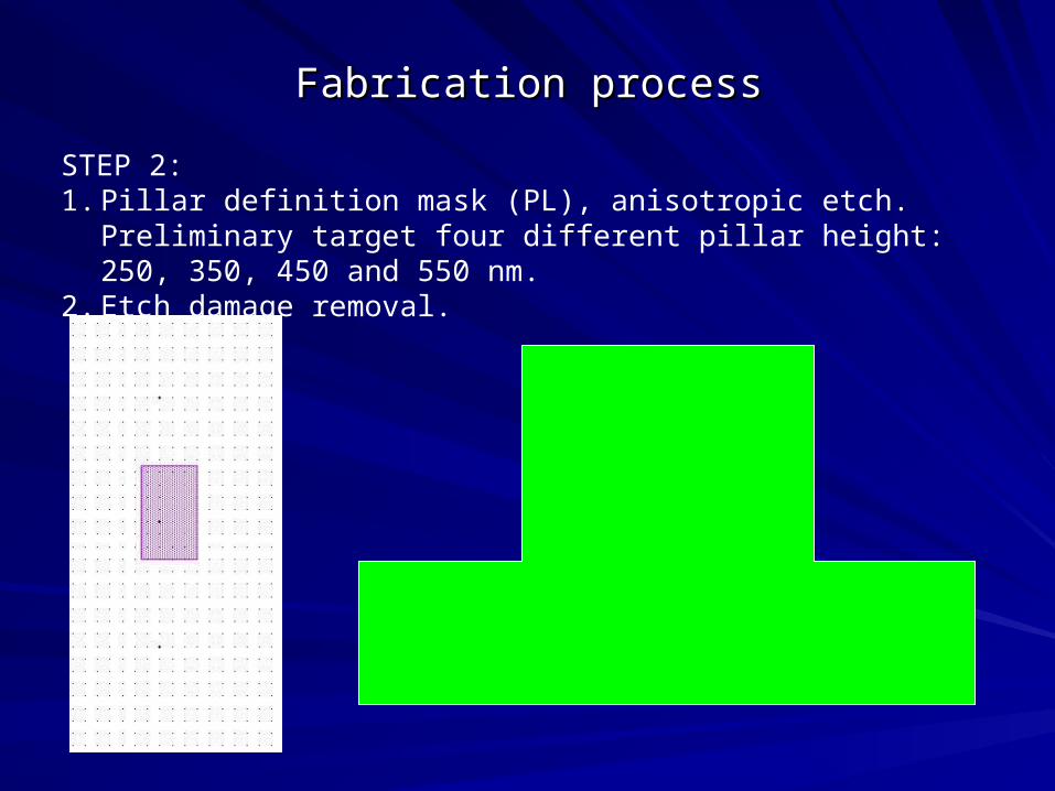
STEP 2:1. Pillar definition mask (PL), anisotropic etch. Preliminary target four
different pillar height: 250, 350, 450 and 550 nm.2. Etch damage removal.

Fabrication processFabrication process
STEP 3: 1. Pad oxidation (dry, 900degC, 10 nm); Pad oxide = stress relief
oxide; protect Si by thermal expansion of Si3N4;2. Deposit Si3N4 (120 nm, 740 degC)

Fabrication processFabrication process
STEP 4: Active area definition 1. Active area definition mask AA; this mask defines the source, the
source contact and the bulk contact area;2. Anisotropic etch

Fabrication processFabrication process
STEP 5: 1. Hydrox oxidation (dry, 1000degC, 400nm); Lateral electrical isolation

Fabrication processFabrication process
STEP 6: 1. Anisotropic etch of Si3N4 and of pad oxide to leave sidewall spacers

Fabrication processFabrication process
STEP 7: FILOX oxidation1. Dry, 1100degC2. Three thicknesses: 40, 70 and 100 nm

Fabrication processFabrication process
STEP 8: Bulk contact implant (p+);1. Mask PP; this mask is larger than the AA to ensure that the bulk
contact covers all of the active area width;2. Implant B+ (1e15cm-3, 50 keV);
Fabrication processFabrication process
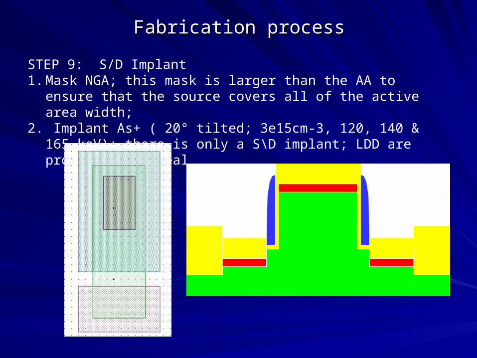
STEP 9: S/D Implant1. Mask NGA; this mask is larger than the AA to ensure that the source
covers all of the active area width;2. Implant As+ ( 20° tilted; 3e15cm-3, 120, 140 & 165 keV); there is
only a S\D implant; LDD are provided by anneal

Fabrication processFabrication process
STEP 10: Nitride fillet and stress relief oxide removal1. Wet etch to remove oxide formed on top of Si3N4;2. Wet etch to remove nitride fillets;3. Wet etch to remove pad (or stress relief) oxide4. 30 nm of FILOX oxide might be removed

Fabrication processFabrication process
STEP 11: Gate oxidation and gate poly deposition. 1. Gate oxidation (dry, 900degC) 2. Deposition of polySi (Low Pressure; 200nm; 5e19cm-3; 650degC)

Fabrication processFabrication process
STEP 12: Poly gate etch1. Mask polysilicon P1; Removal PolySi with anisotropic etch, leaving
only the fillets; 2. The mask protects the link between the Gate contact and the fillets

Fabrication processFabrication process
STEP 13: Back end processing1. Deposition of 100nm undoped Silox+ 500nm BPSG;2. RTA implant activation and reflow3. Mask CW; Vias for metallization

Fabrication processFabrication process
STEP 14: Back end processing1. Sputtering 1000nm Te-Al\Si & Mask M1, Metal lines definition2. Back contact definition for capacitor structures