EECS150 - Digital Design Lecture 7 - High-Level Design ...cs150/fa13/agenda/lec/lec07-hld1.pdf ·...
13
9/19/2013 1 1 Fall 2013 EECS150 - Lec07-hdl1 Page EECS150 - Digital Design Lecture 7 - High-Level Design (Part 1) Sep. 19, 2013 Prof. Ronald Fearing Electrical Engineering and Computer Sciences University of California, Berkeley (slides courtesy of Prof. John Wawrzynek) http://www-inst.eecs.berkeley.edu/~cs150 Outline • Recap: intro to simulation, Verilog to drive and test DUT • High Level Design Overview – divide and conquer – data path/controller partition – organization: e.g. serial vs parallel, pipeline, … 2
Transcript of EECS150 - Digital Design Lecture 7 - High-Level Design ...cs150/fa13/agenda/lec/lec07-hld1.pdf ·...

9/19/2013
1
1 Fall 2013 EECS150 - Lec07-hdl1 Page
EECS150 - Digital Design
Lecture 7 - High-Level Design (Part 1)
Sep. 19, 2013 Prof. Ronald Fearing
Electrical Engineering and Computer Sciences
University of California, Berkeley
(slides courtesy of Prof. John Wawrzynek)
http://www-inst.eecs.berkeley.edu/~cs150
Outline
• Recap: intro to simulation, Verilog to drive and test
DUT
• High Level Design Overview
– divide and conquer
– data path/controller partition
– organization: e.g. serial vs parallel, pipeline, …
2

9/19/2013
2
3 Fall 2013 EECS150 - Lec07-hld1 Page
Introduction
• High-level Design Specifies:
– How data is moved around and operated on.
– The architecture (sometimes called micro-architecture):
• The organization of state elements and combinational logic blocks
• Functional specification of combinational logic blocks
• Optimization
– Deals with the task of modifying an architecture and data movement procedure to meet some particular design requirement:
• performance, cost, power, or some combination.
• high-level organization and optimization – modern CAD tools help fill in the low-level details and optimization
• gate-level minimization, state-assignment, etc.
– A great deal of the leverage on effecting performance, cost, and power comes at the high-level.
3
4 Fall 2013 EECS150 - Lec07-hld1 Page
One Standard High-level Template
• Controller
– accepts external and control input, generates control and external output and sequences the movement of data in the datapath. (puppeteer)
• Datapath
– is responsible for data manipulation. Usually includes a limited amount of storage. (puppet)
• Memory
– optional block used for long term storage of data structures.
• Standard model for CPUs, micro-
controllers, many other digital
sub-systems.
• Usually not nested.
• Sometimes cascaded:

9/19/2013
3
5 Fall 2013 EECS150 - Lec07-hld1 Page
Register Transfer Language
• At the high-level we view these systems as a collection of state
elements and CL blocks.
• “RTL” is a commonly used acronym for “Register Transfer
Level” description.
• It follows from the fact that all synchronous digital system can be
described as a set of state elements connected by combinational
logic blocks.
• Though not strictly correct, some also use “RTL” to mean the
Verilog or VHDL code that describes such systems.
5
6 Fall 2013 EECS150 - Lec07-hld1 Page
Register Transfer “Language” Descriptions
• We introduce a language for
describing the behavior of
systems at the register transfer
level.
• Can view the operation of digital
synchronous systems as a set
of data transfers between
registers with combinational
logic operations happening
during the transfer.
• We will avoid using “RTL” to
mean “register transfer
language.”
• RT Language comprises a set of register transfers with optional operators as part of the transfer.
• Example:
regA ← regB
regC ← regA + regB
if (start==1) regA ← regC
• My personal style:
– use “;” to separate transfers that occur on separate cycles.
– Use “,” to separate transfers that occur on the same cycle.
• Example (2 cycles):
regA ← regB, regB ← 0;
regC ← regA;
9/19/2013
4
7 Fall 2013 EECS150 - Lec07-hld1 Page
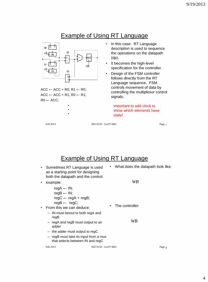
Example of Using RT Language
ACC ← ACC + R0, R1 ← R0;
ACC ← ACC + R1, R0 ← R1;
R0 ← ACC;
•
• •
• In this case: RT Language
description is used to sequence
the operations on the datapath
(dp).
• It becomes the high-level
specification for the controller.
• Design of the FSM controller
follows directly from the RT
Language sequence. FSM
controls movement of data by
controlling the multiplexor control
signals.
clk
clk
clk
important to add clock to
show which elements have
state!
8 Fall 2013 EECS150 - Lec07-hld1 Page
Example of Using RT Language
• Sometimes RT Language is used
as a starting point for designing
both the datapath and the control:
• example:
regA ← IN;
regB ← IN;
regC ← regA + regB;
regB ← regC;
• From this we can deduce:
– IN must fanout to both regA and
regB
– regA and regB must output to an
adder
– the adder must output to regC
– regB must take its input from a mux
that selects between IN and regC
• What does the datapath look like:
• The controller:
WB
WB

9/19/2013
5
9 Fall 2013 EECS150 - Lec07-hld1 Page
List Processor Example
• RT Language gives us a framework for making high-level
optimizations.
• General design procedure outline:
1. Problem, Constraints, and Component Library Spec.
2. “Algorithm” Selection
3. Micro-architecture Specification
4. Analysis of Cost, Performance, Power
5. Optimizations, Variations
6. Detailed Design
9
10 Fall 2013 EECS150 - Lec07-hld1 Page
1. Problem Specification
• Design a circuit that forms the sum of all the 2's complement
integers stored in a linked-list structure starting at memory address
0:
• All integers and pointers are 8-bit. The link-list is stored in a memory
block with an 8-bit address port and 8-bit data port, as shown below.
The pointer from the last element in the list is 0. At least one node in
list.
I/Os:
– START resets to head of list and
starts addition process.
– DONE signals completion
– R holds the final result
Note: We don’t assume nodes are aligned on 2 Byte boundaries.

9/19/2013
6
11 Fall 2013 EECS150 - Lec07-hld1 Page
1. Other Specifications
• Design Constraints: – Usually the design specification puts a restriction on cost,
performance, power or all. We will leave this unspecified for now and return to it later.
• Component Library:
component delay
simple logic gates 0.5ns
n-bit register clk-to-Q=0.5ns
setup=0.5ns
n-bit 2-1 multiplexor 1ns
n-bit adder (2 log(n) + 2)ns
memory 10ns read (asynchronous read)
zero compare 0.5 log(n)
(single ported memory)
Are these reasonable? 11
12 Fall 2013 EECS150 - Lec07-hld1 Page
Review of Register with “Clock Enable”
• Register with Clock Enable:
• Allows register to be either be loaded on selected clock posedge or
to retain its previous value.
• Assume both data and CE require setup time = 0.5ns.
• Assume no reset input.
Functional
description only.
Transistor level
circuit has lower
input delay.
CE
CE

9/19/2013
7
13 Fall 2013 EECS150 - Lec07-hld1 Page
2. Algorithm Specification • In this case the memory only allows one access per cycle, so the algorithm is
limited to sequential execution. If in another case more input data is available
at once, then a more parallel solution may be possible.
• Assume datapath state registers NEXT and SUM.
– NEXT holds a pointer to the node in memory.
– SUM holds the result of adding the node values to this point.
If (START==1) NEXT0, SUM0, DONE0;
repeat {
SUMSUM + Memory[NEXT+1];
NEXTMemory[NEXT];
} until (NEXT==0);
RSUM, DONE1;
13
This RT Language “pseudo code” becomes the basis for DP and controller.
RT language data/control mixing (?)
• sequential?
• interrupted flow?
• parallel operations?
• good for data flow, control better in Verilog…
• state diagram will explain control better! 14
while (START == 0); (1) while (START==1) NEXT0, SUM0, DONE0; begin repeat { SUMSUM + Memory[NEXT+1]; NEXTMemory[NEXT]; } until (NEXT==0); RSUM, DONE1; end while (START==0) DONE1; goto (1)
PSEUDO CODE
but no functions,
actually hardware

9/19/2013
8
15 Fall 2013 EECS150 - Lec07-hld1 Page
3. Architecture #1 Direct implementation of RTL description:
Datapath
Controller
If (START==1) NEXT0, SUM0;
repeat {
SUMSUM + Memory[NEXT+1];
NEXTMemory[NEXT];
} until (NEXT==0);
RSUM, DONE1;
NEXT_SEL=1
WB
16 Fall 2013 EECS150 - Lec07-hld1 Page
4. Analysis of Cost, Performance, and Power
• Skip Power for now.
• Cost:
– How do we measure it? # of transistors? # of gates? # of CLBs?
– Depends on implementation technology. Often we are just
interested in comparing the relative cost of two competing
implementations. (Save this for later)
• Performance:
– 2 clock cycles per number added.
– What is the minimum clock period?
– The controller might be on the critical path. Therefore we need to
know the implementation, and controller input and output delay.
16

9/19/2013
9
17 Fall 2013 EECS150 - Lec07-hld1 Page
Possible Controller Implementation
• Based on this, what is the controller input and output delay?
17
NEXT_SEL=1
draw timing diagram with RTL notation…
one hot
operational timing diagram for list processor
Clock
MemAddress
MemData
LD_SUM
SUM
LD_NEXT
NEXT
18
COMPUTE_SUM GET_NEXT
NEXTMemory[NEXT];
SUMSUM +
Memory[NEXT+1];
x0+x1+x2 x0+x1
5
E A
F
5
GET_NEXT
E x2
E
A
WB

9/19/2013
10
19 Fall 2013 EECS150 - Lec07-hld1 Page
4. Analysis of Performance
Other paths exist for
each cycle in the loop.
These are the worst
case.
20 Fall 2013 EECS150 - Lec07-hld1 Page
4. Analysis of Performance
• Detailed timing:
clock period (T) = max (clock period for each state)
T > 31ns, F < 32 MHz
• Observation:
COMPUTE_SUM state does most of the work. Most of the
components are inactive in GET_NEXT state.
GET_NEXT does: Memory access + …
COMPUTE_SUM does: 8-bit add, memory access, 15-bit add + …
• Conclusion:
Move one of the adds to GET_NEXT.
20
9/19/2013
11
21 Fall 2013 EECS150 - Lec07-hld1 Page
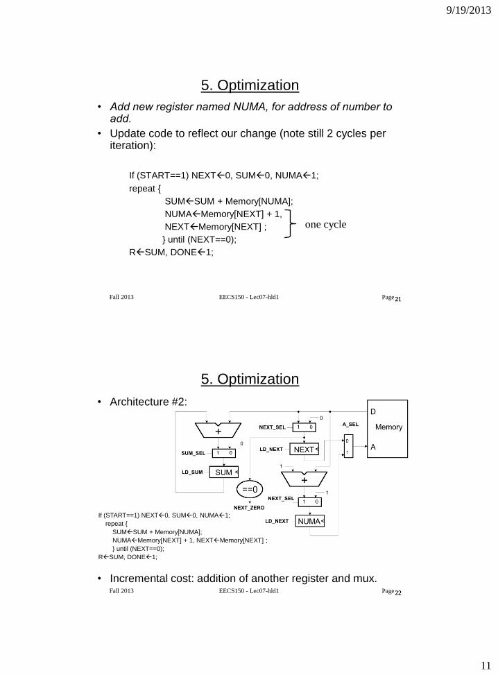
5. Optimization
• Add new register named NUMA, for address of number to add.
• Update code to reflect our change (note still 2 cycles per iteration):
If (START==1) NEXT0, SUM0, NUMA1;
repeat {
SUMSUM + Memory[NUMA];
NUMAMemory[NEXT] + 1,
NEXTMemory[NEXT] ;
} until (NEXT==0);
RSUM, DONE1;
21
one cycle
22 Fall 2013 EECS150 - Lec07-hld1 Page
5. Optimization
• Architecture #2:
• Incremental cost: addition of another register and mux.
If (START==1) NEXT0, SUM0, NUMA1;
repeat {
SUMSUM + Memory[NUMA];
NUMAMemory[NEXT] + 1, NEXTMemory[NEXT] ;
} until (NEXT==0);
RSUM, DONE1;
22

9/19/2013
12
23 Fall 2013 EECS150 - Lec07-hld1 Page
5. Optimization, Architecture #2
• New timing:
Clock Period (T) = max (clock
period for each state)
T > 23ns, F < 43Mhz
• Is this worth the extra cost?
• Can we lower the cost?
• Notice that the circuit now
only performs one add
operation per cycle, but
have two adders. Why not
share 1 adder for both
cycles? 23
24 Fall 2013 EECS150 - Lec07-hld1 Page
5. Optimization, Architecture #3
• Incremental cost:
– Addition of another mux and control (ADD_SEL). Removal of an 8-
bit adder.
• Performance:
– No change.
• Change is definitely worth it.
[Except wiring is more limit than computation…] 24
9/19/2013
13
Summary
• RTL = register transfer level
• FSM is controller
• Load/Enable on register directly corresponds to transfer
command, e.g. A B; (e.g. EnableB, LoadA)
• timing critical for understanding when operations occur
• speed limited by slowest state settling
25