EEC 216 Lecture #9: Energy Recovery Circuitsramirtha/EEC216/W08/lecture9.pdf · EEC 216 Lecture #9:...
60
EEC 216 Lecture #9: Energy Recovery Circuits Rajeevan Amirtharajah University of California, Davis
Transcript of EEC 216 Lecture #9: Energy Recovery Circuitsramirtha/EEC216/W08/lecture9.pdf · EEC 216 Lecture #9:...

EEC 216 Lecture #9:Energy Recovery Circuits
Rajeevan AmirtharajahUniversity of California, Davis

R. Amirtharajah, EEC216 Winter 2008 2
Outline
• Announcements
• Wrap Up: Low Leakage Circuits
• Review: Energy Dissipation
• Adiabatic Charging
• Energy Recovery Circuit Basics
• Dynamic Energy Recovery Logic
• Power and Clock Waveform Generation

R. Amirtharajah, EEC216 Winter 2008 3
Announcements
• Design Project 2 due next Friday, February 29
• Typo: “minimum delay” should be “minimum energy”
• Extra Office Hours: Wednesday, 2/27, 1-3 PM
• Final Projects: start thinking about them!

R. Amirtharajah, EEC216 Winter 2008 4
Suggested Final Projects• Circuits Topics
1. Low power modulated or low-swing interconnect
2. Self-timed and asynchronous circuits for low power
3. Asymmetric blip circuit for pulse-based registers
4. Multiple-threshold logic design
5. Circuits for closed-loop energy harvesting
6. Low leakage memory techniques
7. Low-swing, dual-edge triggered flip-flops

R. Amirtharajah, EEC216 Winter 2008 5
Suggested Final Projects• Architecture Topics
1. Quantifying energy scalability and power awareness
2. Information theoretic and statistical power estimation
3. Power aware instruction set design
4. Fault-tolerance and power consumption
5. Coding for low power
• Miscellaneous Topics1. Energy efficiency of biological computing
2. Energy efficiency of quantum computing
3. Fundamental energy limits of computation
4. Power and energy density implications of molecular electronics

R. Amirtharajah, EEC216 Winter 2008 6
Outline
• Announcements
• Wrap Up: Low Leakage Circuits
• Review: Energy Dissipation
• Adiabatic Charging
• Energy Recovery Circuit Basics
• Dynamic Energy Recovery Logic
• Power and Clock Waveform Generation
R. Amirtharajah, EEC216 Winter 2008 7
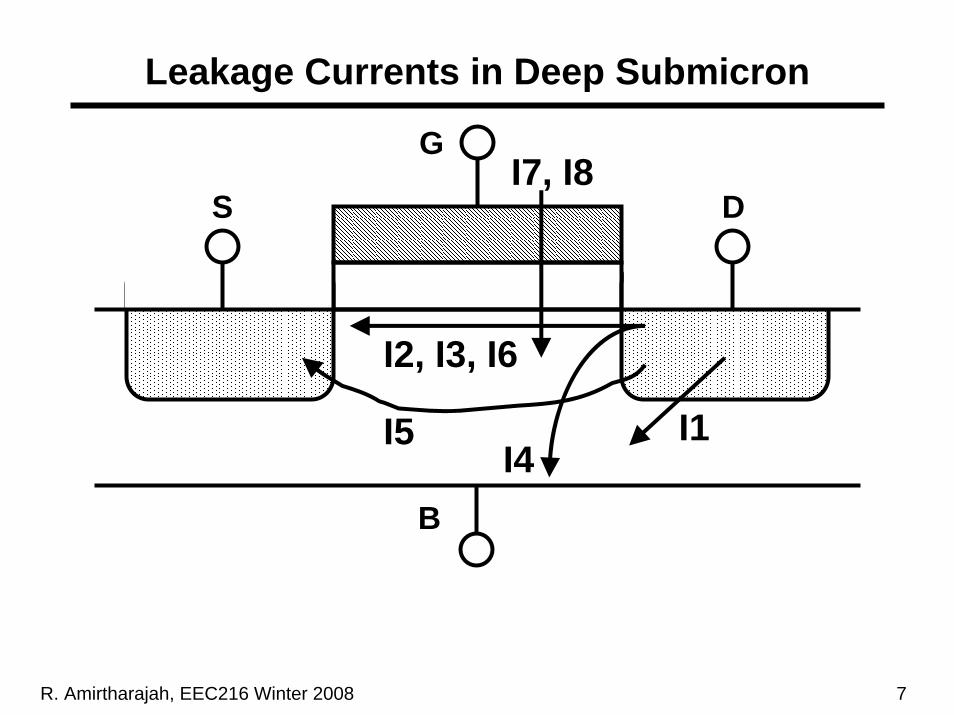
Leakage Currents in Deep Submicron
S D
GI7, I8
I2, I3, I6
I1
B
I4I5

R. Amirtharajah, EEC216 Winter 2008 8
Transistor Leakage Mechanisms1. pn Reverse Bias Current (I1)
2. Subthreshold (Weak Inversion) (I2)
3. Drain Induced Barrier Lowering (I3)
4. Gate Induced Drain Leakage (I4)
5. Punchthrough (I5)
6. Narrow Width Effect (I6)
7. Gate Oxide Tunneling (I7)
8. Hot Carrier Injection (I8)
R. Amirtharajah, EEC216 Winter 2008 9
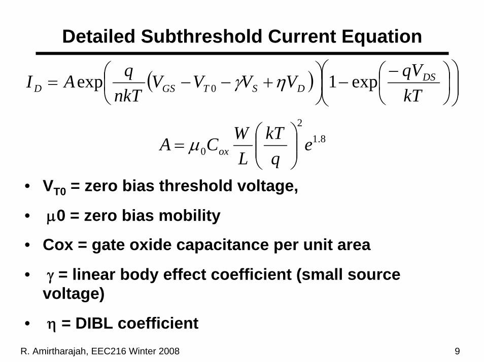
Detailed Subthreshold Current Equation
( ) ⎟⎟⎠
⎞⎜⎜⎝
⎛⎟⎠⎞
⎜⎝⎛ −−⎟
⎠⎞
⎜⎝⎛ +−−=
kTqVVVVV
nkTqAI DS
DSTGSD exp1exp 0 ηγ
• VT0 = zero bias threshold voltage,
• μ0 = zero bias mobility
• Cox = gate oxide capacitance per unit area
• γ = linear body effect coefficient (small source voltage)
• η = DIBL coefficient
8.12
0 eq
kTLWCA ox ⎟⎟
⎠
⎞⎜⎜⎝
⎛= μ
R. Amirtharajah, EEC216 Winter 2008 10
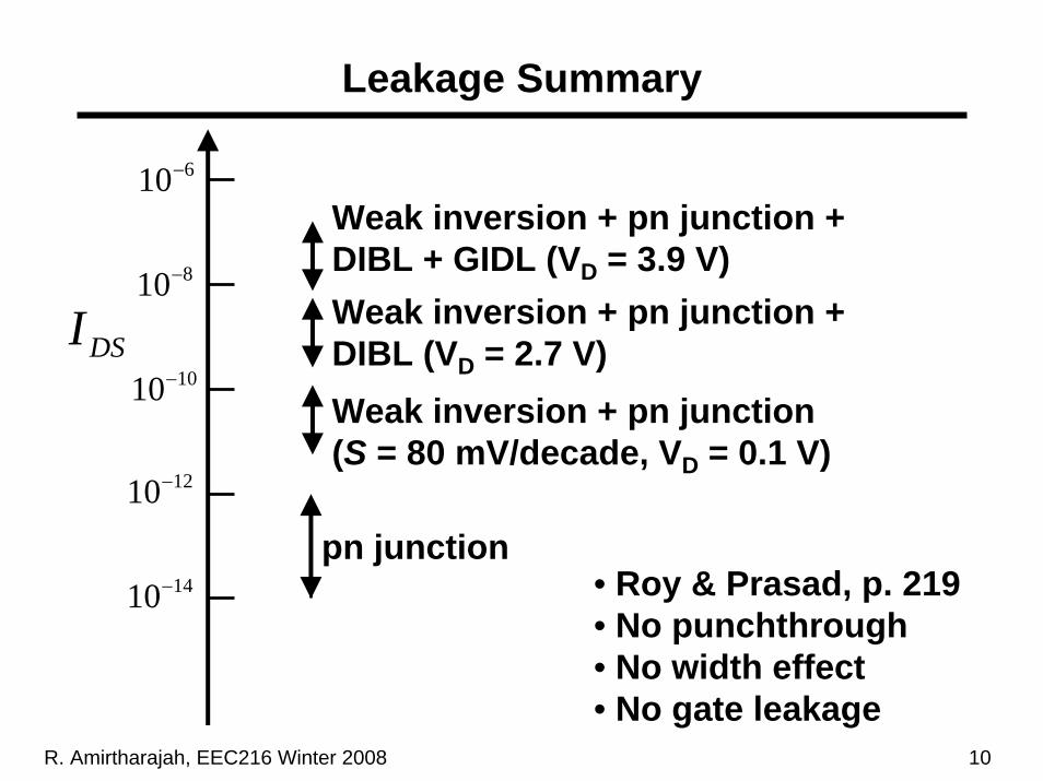
Leakage Summary
DSI
1210−
1010−
810−
610−
pn junction• Roy & Prasad, p. 219• No punchthrough• No width effect• No gate leakage
1410−
Weak inversion + pn junction(S = 80 mV/decade, VD = 0.1 V)
Weak inversion + pn junction +DIBL (VD = 2.7 V)
Weak inversion + pn junction +DIBL + GIDL (VD = 3.9 V)

R. Amirtharajah, EEC216 Winter 2008 11
Outline
• Announcements
• Wrap Up: Low Leakage Circuits
• Review: Energy Dissipation
• Adiabatic Charging
• Energy Recovery Circuit Basics
• Dynamic Energy Recovery Logic
• Power and Clock Waveform Generation
R. Amirtharajah, EEC216 Winter 2008 12
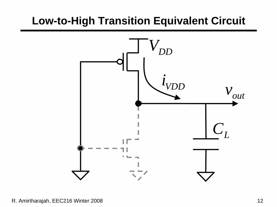
Low-to-High Transition Equivalent Circuit
LC
VDDioutv
DDV

R. Amirtharajah, EEC216 Winter 2008 13
Energy Drawn From Power Supply
dtVtidttPE DDVDDVDDVDD ∫∫∞∞
==00
)()(
∫∫ ==∞ DDV
outDDLout
LDD dvVCdtdt
dvCV00
2DDLVC=
)(tvout )(tiVDD

R. Amirtharajah, EEC216 Winter 2008 14
Energy Stored on Load Capacitor
• Compared to , we see that dissipated
• Same amount dissipated when capacitor discharged
• Independent of MOSFET resistance
dtvtiE outVDDC ∫∞
=0
)(
∫∫ ==∞ DDV
outoutLoutout
L dvvCdtvdt
dvC00
2
21
DDLVC=
2
2DDLVC
VDDE

R. Amirtharajah, EEC216 Winter 2008 15
Can We Do Better on Energy?
• Seems that is pretty fundamental
– Independent of resistance, circuit delay
• Static CMOS logic basically configures FETs as switches connected to voltage sources
– Transient determined by capacitor dynamics,
• But, suppose we use a current source to charge the capacitor instead…
2DDLVC
LRC

R. Amirtharajah, EEC216 Winter 2008 16
Outline
• Announcements
• Wrap Up: Low Leakage Circuits
• Review: Energy Dissipation
• Adiabatic Charging
• Energy Recovery Circuit Basics
• Dynamic Energy Recovery Logic
• Power and Clock Waveform Generation

R. Amirtharajah, EEC216 Winter 2008 17
Principle of Adiabatic Charging
dttvtiE IDDDDIDD )()(0∫∞
=
LC
R
)(tiDD
• By controlling the current, we can control the voltage developed across the resistor, and reduce power consumption by charging slowly

R. Amirtharajah, EEC216 Winter 2008 18
Adiabatic Charging Analysis
cc V
dtdVRC +⎟
⎠⎞
⎜⎝⎛=Φ
LC
R
)(tΦ
• Solve differential equation assuming input is ramp with duration T
)(tVc

R. Amirtharajah, EEC216 Winter 2008 19
Input Voltage Equation
• ideal linear voltage ramp ending in VDD steady-state voltage
• Later: how to implement impacts energy dissipation and limits energy recovery efficiency
⎪⎪⎩
⎪⎪⎨
⎧
≥
<≤
<
=Φ
TtV
TttT
Vt
t
DD
DD 0
00
)(
)(tΦ
)(tΦ

R. Amirtharajah, EEC216 Winter 2008 20
Output Voltage Solution
• Solve for instantaneous resistor power using
• Integrate to find dissipated energy as function of T
)(tVc
( )( )⎪
⎪⎪
⎩
⎪⎪⎪
⎨
⎧
≥−−Φ
<≤−−Φ
<
=
−−−
−
TteeVT
RC
TteVT
RCt
tV
RCTtRCTDD
RCtDDc
)(1
01
00
)(

R. Amirtharajah, EEC216 Winter 2008 21
Energy Dissipated With Ramp Driver
• Consider the extreme cases of RC with respect to T
( ) ( )( ) dtR
tVdttVtiE cRRdiss ∫∫
∞∞ −Φ==
0
2
0
)(
⎥⎦⎤
⎢⎣⎡ +−= − RCT
DD eT
RCT
RCCVT
RC 12
( )( ) ( )( ) dtR
tVdtR
tV
T
cT
c ∫∫∞ −Φ
+−Φ
=2
0
2

R. Amirtharajah, EEC216 Winter 2008 22
Limiting Cases of Slow and Fast Ramps
• For very slow ramp :
• For very fast ramp (original CMOS case):
• Energy dissipation can be made arbitrarily small by making transition time T arbitrarily long
2DDdiss CV
TRCE =
RCT >>
2
21
DDdiss CVE =
RCT <<

R. Amirtharajah, EEC216 Winter 2008 23
Example Voltage Ramp: Stepwise Charging
TC+
−
1−NV
TC+
−
1V
TC+
−
0V
ΦNΦN-1
Φ1
Φ0
ΦGND
Out
outv

R. Amirtharajah, EEC216 Winter 2008 24
Stepwise Charger Operation
• Basic idea: charge large capacitance in small incremental steps– Voltage swing between steps small, so small power
dissipation between intermediate voltage levels– Falls off quadratically with number of levels N– N steps required, so total dissipation for entire
transition goes as 1 / N
fN
VC DDL
2
=
2
1∑=
⎟⎠⎞
⎜⎝⎛=
N
k
DDL N
VCfP
R. Amirtharajah, EEC216 Winter 2008 25
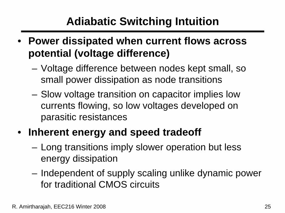
Adiabatic Switching Intuition
• Power dissipated when current flows across potential (voltage difference)– Voltage difference between nodes kept small, so
small power dissipation as node transitions– Slow voltage transition on capacitor implies low
currents flowing, so low voltages developed on parasitic resistances
• Inherent energy and speed tradeoff– Long transitions imply slower operation but less
energy dissipation– Independent of supply scaling unlike dynamic power
for traditional CMOS circuits

R. Amirtharajah, EEC216 Winter 2008 26
Outline
• Announcements
• Wrap Up: Low Leakage Circuits
• Review: Energy Dissipation
• Adiabatic Charging
• Energy Recovery Circuit Basics
• Dynamic Energy Recovery Logic
• Power and Clock Waveform Generation
R. Amirtharajah, EEC216 Winter 2008 27
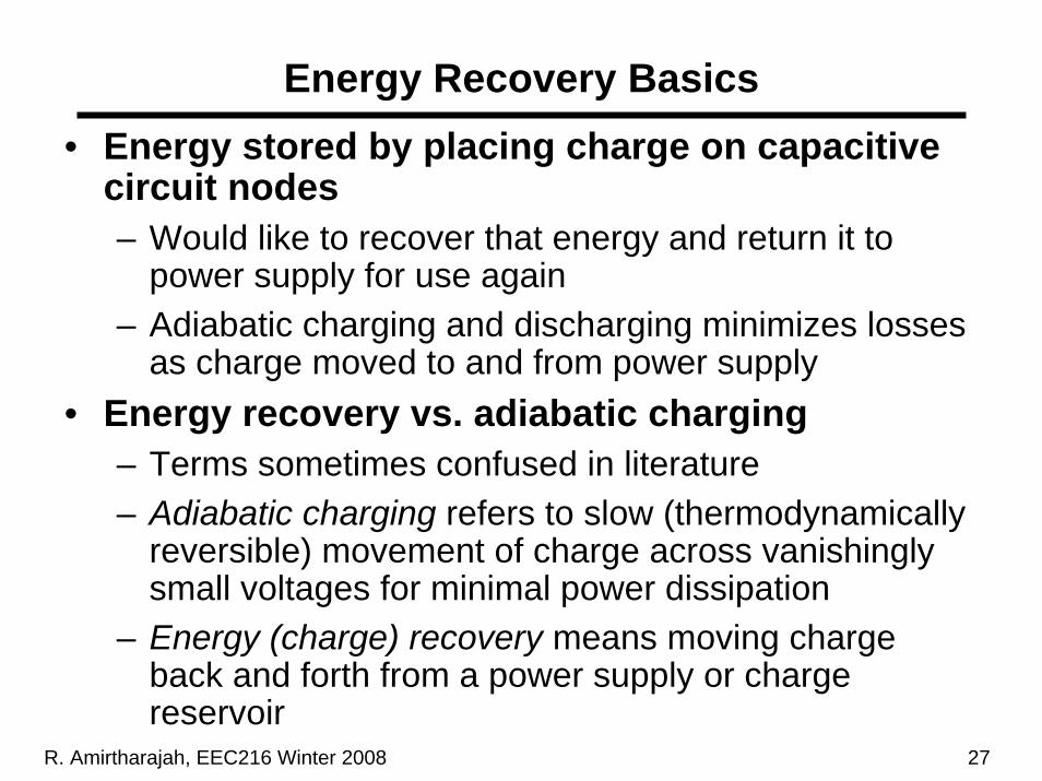
Energy Recovery Basics• Energy stored by placing charge on capacitive
circuit nodes– Would like to recover that energy and return it to
power supply for use again– Adiabatic charging and discharging minimizes losses
as charge moved to and from power supply• Energy recovery vs. adiabatic charging
– Terms sometimes confused in literature– Adiabatic charging refers to slow (thermodynamically
reversible) movement of charge across vanishingly small voltages for minimal power dissipation
– Energy (charge) recovery means moving charge back and forth from a power supply or charge reservoir

R. Amirtharajah, EEC216 Winter 2008 28
Energy Recovery Process
LC
cioutv
)(tΦ

R. Amirtharajah, EEC216 Winter 2008 29
Energy Recovery Timing Phases
• Similar to dynamic logic or level sensitive (latch-based) clocking, except power supply is also the clock signal
• Four phases of operation– Idle Phase: (Φ = 0) Circuit state before evaluation– Evaluation Phase: (Φ transitions from 0 V to VDD)
Circuit nodes evaluate to final value– Hold Phase: (Φ = VDD) Circuit nodes maintain state
after evaluation– Restoration Phase: (Φ transitions from VDD to 0 V )
Circuit nodes restored to initial value

R. Amirtharajah, EEC216 Winter 2008 30
Energy Recovery Process Timing
outv
)(tΦ
• Want output voltage to transition slowly with power/clock waveform
• How do we cascade logic stages?

R. Amirtharajah, EEC216 Winter 2008 31
Cascading Energy Recovery Stages
0y
0Φ
?
1y
1Φ
?

R. Amirtharajah, EEC216 Winter 2008 32
Cascaded Logic Energy Recovery Timing
• Charge nth stage nodes and then discharge (n-1)th stage nodes
• How do we implement the energy recovery phase?
0y
0Φ
1y
1Φ

R. Amirtharajah, EEC216 Winter 2008 33
Cascaded Logic Timing Issues
• Must isolate input from output node– Otherwise inputs cannot change until output has
been sampled by succeeding stage– Constraint ripples to end of logic pipeline, i.e. no
input can change until final stage evaluates• Isolation requires an alternative path (? Box) for
reverse current flow for energy recovery – Reverse path must be controlled by gate output– If y0 = 1, then must discharge y0 slowly using Φ0
(returning charge to power supply)– If y0 = 0, reverse path must be open circuit to prevent
leakage from Φ0 contaminating output y0
R. Amirtharajah, EEC216 Winter 2008 34
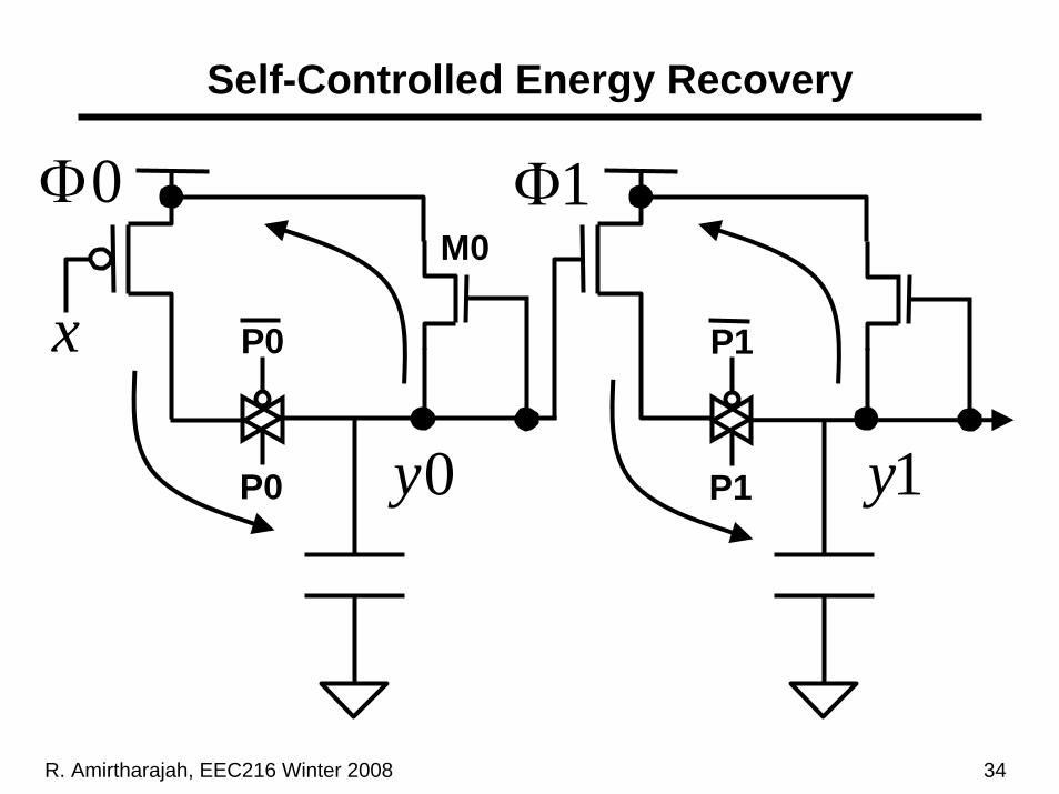
Self-Controlled Energy Recovery
0y
0Φ
1y
1Φ
x
P0
P0
P1
P1
M0

R. Amirtharajah, EEC216 Winter 2008 35
Self-Controlled Recovery Issues
• Use full transmission gates to isolate outputs• Diode connect FETs between output and clock /
power node provide reverse current path for energy recovery – Simple to implement with low area overhead– Control signal varying with output voltage transition– Requires VTH voltage drop to forward bias diode M0,
increasing power dissipation• Would like recovery path control signal to
maintain state throughout restoration phase • Alternative: use succeeding stage output to
compute control

R. Amirtharajah, EEC216 Winter 2008 36
Next Stage Controlled Energy Recovery
0y
0Φ
1y
1Φ
xP0
P0
P1
P1
0F 1F
11−F
1Φ

R. Amirtharajah, EEC216 Winter 2008 37
Next Stage Controlled Recovery Issues• Control signal for energy recovery path generated
from succeeding stage output– Requires computing inverse function of nth stage to
reproduce state of (n-1)th stage output– Full pass gate isolation means that control signal held
constant during full restoration phase transition• Overhead for this logic style can be high
– Computing inverse could be even more area intensive than computing desired function
• True physically and logically reversible computation– Pass gate reverse current path has little loss, adiabatic
transition– Style results in minimum overall energy dissipation

R. Amirtharajah, EEC216 Winter 2008 38
Example: Split-Level Charge Recovery Logic
AZ
0Φ
0Φ
1P
1P
• Uses rails which split up and down from half VDDrather than single rail ramping from 0V to VDD
• Can use many clock phases to build pipeline
• Younis 1994

R. Amirtharajah, EEC216 Winter 2008 39
Energy Recovery System Block Diagram
• Use circuits to generate power / clock waveforms• Generators must use as little power as possible
– Resonant RLC circuits often used in these applications
– Minimize parasitic losses in power / clock generator
DCAC
CLOCK / POWERDRIVER
ENERGY RECOVERY
LOGIC
NΦΦ K0DDV

R. Amirtharajah, EEC216 Winter 2008 40
Outline
• Announcements
• Wrap Up: Low Leakage Circuits
• Review: Energy Dissipation
• Adiabatic Charging
• Energy Recovery Circuit Basics
• Dynamic Energy Recovery Logic
• Power and Clock Waveform Generation

R. Amirtharajah, EEC216 Winter 2008 41
Dynamic CMOS Two-Input NAND Gate
A
• PMOS precharges (Clk low), NMOS evaluates (Clk high)
B
OutClk
Clk

R. Amirtharajah, EEC216 Winter 2008 42
Adiabatic Dynamic Logic (ADL) Inverter
LCinV
outV
Φ• Precharge Phase: Φ0 is long voltage ramp from 0V
to VDD charging Vout to VDD- Vdiode
• Evaluate Phase: Φ0 swings slowly low, discharging if input is high otherwise leaving output high

R. Amirtharajah, EEC216 Winter 2008 43
Cascading Adiabatic Dynamic Logic Gates
iC1−iX
iX
0Φ• Similar to NP-CMOS design style: cascade N-
blocks with P-blocks
1+iC
1+iX
1Φ

R. Amirtharajah, EEC216 Winter 2008 44
Adiabatic Dynamic Logic Design Issues• Clocking methodology similar to all adiabatic
designs: four phases required – Clocks for consecutive stages must be synchronized
such that when the output of first stage is latched (hold phase) the second stage starts evaluate phase
– When first stage is evaluating, must ensure no non-adiabatic transitions in second stage
• Output voltages must be precharged high (low) enough to guarantee correct operation– Reduces to guaranteeing diode drop is significantly
less than FET threshold voltage (Vdiode < VTH)– Alternative is to add DC offset to power / clock
voltages to compensate for diode drop

R. Amirtharajah, EEC216 Winter 2008 45
Cascaded Adiabatic Dynamic Logic Timing
• Consecutive stages have opposite clock polarities– Similar to NP-CMOS dynamic logic clocking
• Four phases are actually necessary– In this example, stage clocked by Φ2 evaluates
while Φ1 holds and Φ0 restores• Feedback must occur every four stages for
consistent timing (every 4th stage in same phase)
0Φ
1Φ

R. Amirtharajah, EEC216 Winter 2008 46
Adiabatic Dynamic Logic NAND2
LCA
outV
Φ• Complex ADL gate design similar to dynamic
CMOS logic design:– Implement arbitrary pulldown network with a diode
in parallel
B

R. Amirtharajah, EEC216 Winter 2008 47
Outline
• Announcements
• Wrap Up: Low Leakage Circuits
• Review: Energy Dissipation
• Adiabatic Charging
• Energy Recovery Circuit Basics
• Dynamic Energy Recovery Logic
• Power and Clock Waveform Generation

R. Amirtharajah, EEC216 Winter 2008 48
Supply Clock Generation Goals• Energy recovery logic requires efficient power /
clock waveform generation– Should operate with high efficiency (low loss) at high
frequency– Must create long rise and fall times for adiabatic
charging of capacitive circuit nodes– Must be able to deliver and receive charge to recover
energy• Stepwise driver incorporates too many losses to
satisfy these requirements well• Most approaches use an RLC resonant circuit
– Sinusoidal slope approximates linear ramp– Energy moved between capacitive nodes and inductor

R. Amirtharajah, EEC216 Winter 2008 49
Basic Resonant Clock Generator
• SW0 closes, Φ rings up to VDD or down to ground• MP or MN turns on to hold Φ at steady state• RC models clock net, L chosen to set frequency
C
ΦVDD/2
RL
VDD
SW0MP
MN
R. Amirtharajah, EEC216 Winter 2008 50
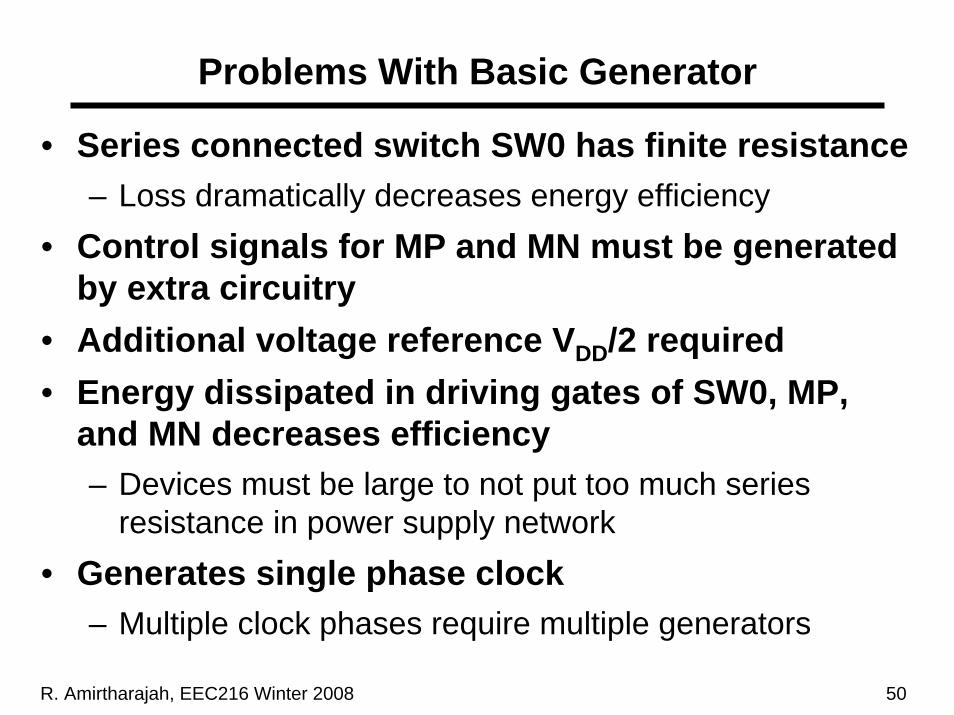
Problems With Basic Generator
• Series connected switch SW0 has finite resistance– Loss dramatically decreases energy efficiency
• Control signals for MP and MN must be generated by extra circuitry
• Additional voltage reference VDD/2 required• Energy dissipated in driving gates of SW0, MP,
and MN decreases efficiency– Devices must be large to not put too much series
resistance in power supply network• Generates single phase clock
– Multiple clock phases require multiple generators

R. Amirtharajah, EEC216 Winter 2008 51
Half Blip Circuit Operation
• Alternative topology for a single rail resonant driver • Eliminates series losses since reset NMOS in parallel• Athas et al., JSSC 97

R. Amirtharajah, EEC216 Winter 2008 52
Original Blip Circuit
• Transistors MN0 and MN1 restore energy to oscillator dissipated by lossy elements
• Generates two almost nonoverlapping clock phases• Gates are also driven resonantly by circuit
VDD/2
C
0Φ RL
MN0C
1ΦR L
MN1

R. Amirtharajah, EEC216 Winter 2008 53
Full Blip Circuit Operation
• Nonoverlapping clock generation measured traces• Athas et al., JSSC 97

R. Amirtharajah, EEC216 Winter 2008 54
Blip Circuit Issues
• Nonsinusoidal “blip” waveforms produced since there are no pullup paths– Sinusoidal waveform has highest energy recycling
efficiency for a resonant circuit– Energy recovery is most efficient at fundamental
frequency– Energy in higher order harmonics almost totally lost
• Two inductors and half VDD reference required for the basic circuit

R. Amirtharajah, EEC216 Winter 2008 55
Blip Circuit Variation 1
• PMOS pullup MP0 used in one branch of circuit• Generates closer to sinusoidal output for better
energy efficiency• PMOS must be sized larger for same resistance,
more loss when driving MP0 gate
VDD/2
C
0Φ RL
MN0C
1ΦR L
MP0
VDD
R. Amirtharajah, EEC216 Winter 2008 56
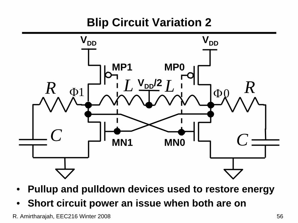
Blip Circuit Variation 2
VDD/2
C
0Φ RL
MN0C
1ΦR L
MN1
MP0MP1
VDD VDD
• Pullup and pulldown devices used to restore energy• Short circuit power an issue when both are on

R. Amirtharajah, EEC216 Winter 2008 57
Other Blip Circuit Variations
• Control PMOS and NMOS gates separately– Careful rise and fall time management of control signals
improves efficiency, creates mostly sinusoidal output– Never on simultaneously so no short circuit power– Requires PLL to align control signals properly in time,
whereas blip circuit control was fully self-timed– Control device gates not driven resonantly so additional
power dissipation there• Other supply clock schemes proposed including
using MEMS switches, MEMS resonators, etc.
R. Amirtharajah, EEC216 Winter 2008 58
Mixing Energy Recovery and Standard Logic
• Can apply energy recovery selectively to design• Most useful for high capacitance nodes like
clocks, enables, memory word lines and bit lines, other global signals
• Get some power benefits without overhead of circuit reversibility, especially for simple functions like clocks
• Decreased time for circuit redesign• Requires careful interfacing between energy
recovery and traditional circuit styles to guarantee correct operation

R. Amirtharajah, EEC216 Winter 2008 59
AC-1 Microprocessor Example
• Used energy recovery latches with traditional logic• Athas et al., JSSC 97

R. Amirtharajah, EEC216 Winter 2008 60
Energy Recovery Logic Summary
• Adiabatic charging and energy recovery can result in asymptotically zero energy dissipation– Requires operation to be arbitrarily slow– Not all applications amenable to very low frequency
operation• Diode based approaches dissipate more power
– Finite forward biased diode drops inherently burn power– Full transmission gate circuits are better from power
perspective• Leakage power currently limits usefulness
– Energy recovery techniques apply to dynamic power only, if leakage dominates then not much gain
– Active research to address these concerns