EE542 Microwave Engineering - KAISTma.kaist.ac.kr/lecturenote/2014_Fall/1_Course overview.pdf · 7...
33
1 EE542 Microwave Engineering, Lecture Times: Tue. 14:30~15:45/ Thu. 14:30~15:45 Location: E3-2 Building, #2220 Professor: Seong-Ook Park, Ph. D. Tel: 350-7414, E-mail: [email protected] Office Hours: E3-2 Building, #6-5206, Wed: 11:00AM~12:00 or by appointment Course Objectives: The goal of this course is to introduce students to the concepts and principles of the advanced microwave engineering, including the use of computer aided design(CAD) methods. RF/microwave CAD is employed extensively in industry and a knowledge of the principles and methods used is important for anyone who may work in an RF/microwave related field. Theory and design of passive and active microwave components, and microwave circuits including: microstrip line, guided wave device, filter, amplifier, oscillators, and experimental characterization of above components using the network analyzer, power and noise meters, microwave theory and properties of ferrimagnetic material. The general flow of this class is Application --> System --> Component; individual components are analyzed by Fields --> Modes --> Equivalent Network. Computer Usage: Computer aides design tools, such as ADS, are used to design, analyze, and construct RF and Microwave Circuits and Matlab EE542 Microwave Engineering 2014 Fall Semester Park, 2014 Fall, KAIST
Transcript of EE542 Microwave Engineering - KAISTma.kaist.ac.kr/lecturenote/2014_Fall/1_Course overview.pdf · 7...

S.-O. Park, KAIST 1 EE542 Microwave Engineering,
Lecture Times: Tue. 14:30~15:45/ Thu. 14:30~15:45
Location: E3-2 Building, #2220
Professor: Seong-Ook Park, Ph. D. Tel: 350-7414, E-mail: [email protected]
Office Hours: E3-2 Building, #6-5206, Wed: 11:00AM~12:00 or by appointment
Course Objectives:
The goal of this course is to introduce students to the concepts and principles of the advanced
microwave engineering, including the use of computer aided design(CAD) methods.
RF/microwave CAD is employed extensively in industry and a knowledge of the principles and
methods used is important for anyone who may work in an RF/microwave related field. Theory
and design of passive and active microwave components, and microwave circuits including:
microstrip line, guided wave device, filter, amplifier, oscillators, and experimental
characterization of above components using the network analyzer, power and noise meters,
microwave theory and properties of ferrimagnetic material.
The general flow of this class is Application --> System --> Component; individual
components are analyzed by Fields --> Modes --> Equivalent Network.
Computer Usage:
Computer aides design tools, such as ADS, are used to design, analyze, and
construct RF and Microwave Circuits and Matlab
EE542 Microwave Engineering 2014 Fall Semester
Park, 2014 Fall, KAIST

S.-O. Park, KAIST 2
Welcome –
Instructor: Prof. Seong-Ook Park
Office: E3-2 Building, #6-5206
Email: [email protected]
Phone: 350-7414 (010-3412-1451)
Office hours – 11:00 AM ~ 12:00 (Wed.)
or by appointment
Assistant: Byung Kwan Kim, (010-3055-3536)
Email: [email protected]
Formulate good questions and seek the
answers.
EE542 Microwave Engineering, Park, 2014 Fall, KAIST

S.-O. Park, KAIST 3
Graduate Course webpage:
http://ma.kaist.ac.kr/lecturenote/2014_Fall/
Text: Lecture Note & Paper
Tentative grading distribution
Mid-Term Exam 35 %
Term-Proj 35 %
Homework 25%
Attendance 5%
Total 100 %
EE542 Microwave Engineering, Park, 2013 Fall, KAIST Park, 2014 Fall, KAIST

S.-O. Park, KAIST 4
Maxwell Equation for Waves
Maxwell’s Equations for fields in free space are given by
E :Electric Field intensity (volt/meter)
H : Magnetic Field intensity (amperes/meter
D :Electric Flux density (coulombs/meter2)
B : Magnetic Flux density (webers/meter2)
(Constitutive Parameters and Relationships)
We recall that D=eE, B=mH, and J=sE + Jf´, where s is conductivity and Jf´is the free current density arising from sources other than conductivity. Assuming that there are no external free charge and currents in the region of interest, that is, we can take J = 0, r = 0 and Jf´=0.
0
0
HE
t
EH J
t
B
E
m
e
r
e
=
=
=
=
EE542 Microwave Engineering, Park, 2013. Fall, KAIST Park, 2014 Fall, KAIST
S.-O. Park, KAIST 5
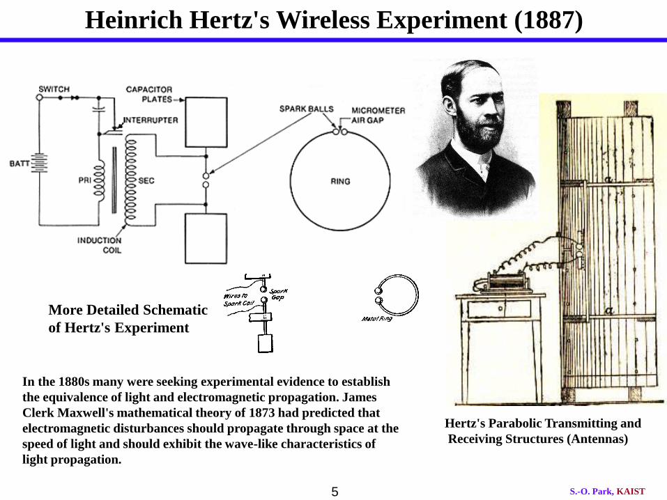
Hertz's Parabolic Transmitting and
Receiving Structures (Antennas)
More Detailed Schematic
of Hertz's Experiment
In the 1880s many were seeking experimental evidence to establish
the equivalence of light and electromagnetic propagation. James
Clerk Maxwell's mathematical theory of 1873 had predicted that
electromagnetic disturbances should propagate through space at the
speed of light and should exhibit the wave-like characteristics of
light propagation.
Heinrich Hertz's Wireless Experiment (1887)

S.-O. Park, KAIST 6
The Electromagnetic Spectrum
EE542 Microwave Engineering, Park, 2013. Fall, KAIST Park, 2014 Fall, KAIST

S.-O. Park, KAIST 7
7
The index of refraction (first graph)
and absorption coefficient (second
graph) of liquid water as a function
of linear frequency. From J. D.
Jackson, Classical Electrodynamics
(2nd edition), John Wiley & Sons,
Inc., New York (1975).
The absorption coefficient falls precipitously over
7.5 decades to a value of a 3 10 -3 cm-1 in a
narrow frequency range between 4 1014Hz and 8
1014Hz.
This is a dramatic absorption window in what what
we call the visible region. The extreme transparency
of water here has it’s origins in the basic energy
level structure of the atoms and molecules.
The student may meditate on the fundamental
question of biological evolution on this water soaked
planet, or why animal eyes see the spectrum from
red to violate and of why the grass is green. Mother
nature has certainly exploited her window!
Park, 2014 Fall, KAIST EE542 Microwave Engineering,
S.-O. Park, KAIST 8
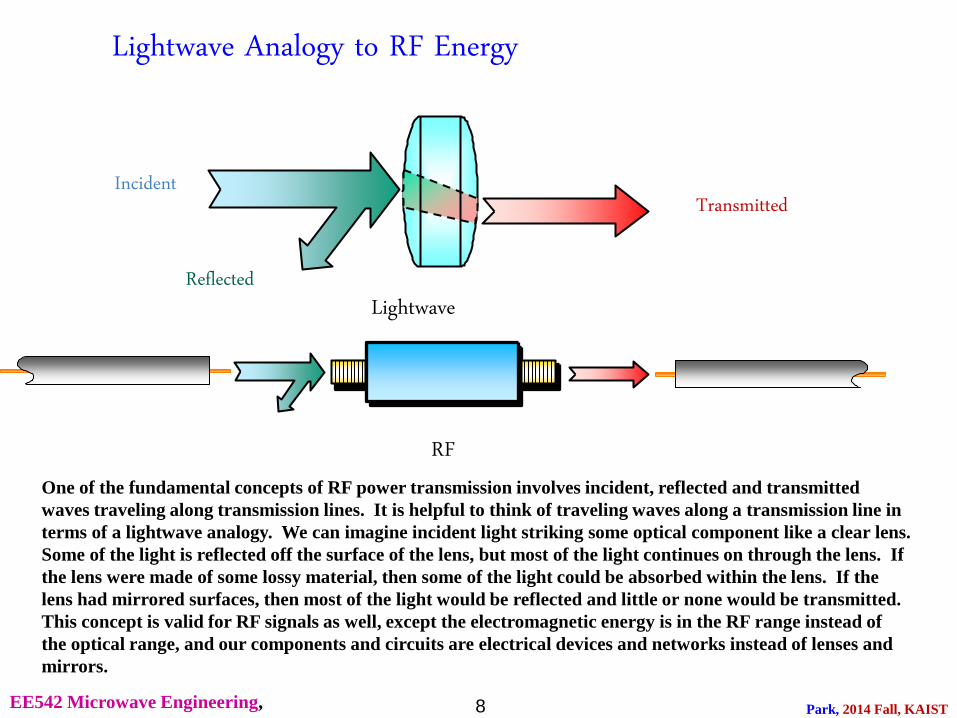
Lightwave Analogy to RF Energy
RF
Incident
Reflected
Transmitted
Lightwave
One of the fundamental concepts of RF power transmission involves incident, reflected and transmitted
waves traveling along transmission lines. It is helpful to think of traveling waves along a transmission line in
terms of a lightwave analogy. We can imagine incident light striking some optical component like a clear lens.
Some of the light is reflected off the surface of the lens, but most of the light continues on through the lens. If
the lens were made of some lossy material, then some of the light could be absorbed within the lens. If the
lens had mirrored surfaces, then most of the light would be reflected and little or none would be transmitted.
This concept is valid for RF signals as well, except the electromagnetic energy is in the RF range instead of
the optical range, and our components and circuits are electrical devices and networks instead of lenses and
mirrors.
EE542 Microwave Engineering, Park, 2013 Fall, KAIST Park, 2014 Fall, KAIST
S.-O. Park, KAIST 9
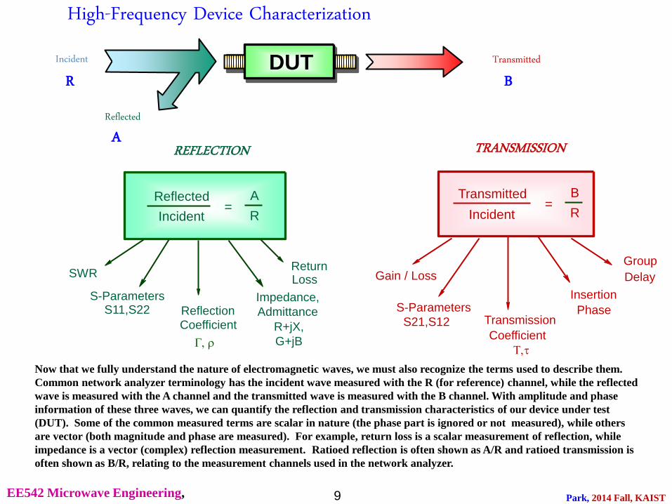
High-Frequency Device Characterization
Reflected
Incident
REFLECTION
SWR
S-Parameters S11,S22 Reflection
Coefficient
Impedance,
Admittance
R+jX,
G+jB
Return Loss
G, r
A
R =
Transmitted
Incident
TRANSMISSION
Gain / Loss
S-Parameters
S21,S12
Group
Delay
Transmission
Coefficient
Insertion
Phase
T,t
B
R =
R
A
Incident
Reflected
B
Transmitted DUT
Now that we fully understand the nature of electromagnetic waves, we must also recognize the terms used to describe them.
Common network analyzer terminology has the incident wave measured with the R (for reference) channel, while the reflected
wave is measured with the A channel and the transmitted wave is measured with the B channel. With amplitude and phase
information of these three waves, we can quantify the reflection and transmission characteristics of our device under test
(DUT). Some of the common measured terms are scalar in nature (the phase part is ignored or not measured), while others
are vector (both magnitude and phase are measured). For example, return loss is a scalar measurement of reflection, while
impedance is a vector (complex) reflection measurement. Ratioed reflection is often shown as A/R and ratioed transmission is
often shown as B/R, relating to the measurement channels used in the network analyzer.
EE542 Microwave Engineering, Park, 2012 Fall, KAIST Park, 2014 Fall, KAIST
S.-O. Park, KAIST 10
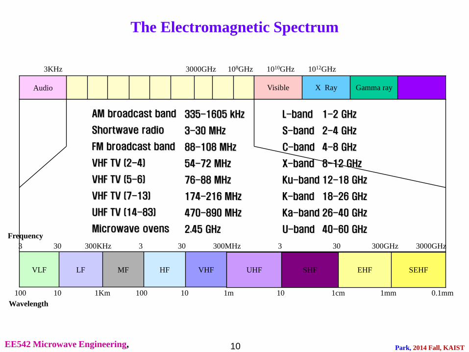
Gamma ray X Ray Visible
The Electromagnetic Spectrum
Audio
3KHz 3000GHz 108GHz 1010GHz 1012GHz
VHF HF MF LF VLF SEHF EHF SHF UHF
3 30 300KHz 3 30 300MHz 3 30 300GHz 3000GHz
100 10 1Km 100 10 1m 10 1cm 1mm 0.1mm
Frequency
Wavelength
AM broadcast band
Shortwave radio
FM broadcast band
VHF TV (2-4)
VHF TV (5-6)
VHF TV (7-13)
UHF TV (14-83)
Microwave ovens
335-1605 kHz
3-30 MHz
88-108 MHz
54-72 MHz
76-88 MHz
174-216 MHz
470-890 MHz
2.45 GHz
L-band
S-band
C-band
X-band
Ku-band
K-band
Ka-band
U-band
1-2 GHz
2-4 GHz
4-8 GHz
8-12 GHz
12-18 GHz
18-26 GHz
26-40 GHz
40-60 GHz
EE542 Microwave Engineering, Park, 2013. Fall, KAIST Park, 2014 Fall, KAIST

S.-O. Park, KAIST 11
Fly’s-eye view. (Adult eye shown here.)
Medium 1
Medium 2
Sub-wavelength Device in Optics and Microwave
<1.6mm
0.5mm
Visible Light: 0.4mm~0.8mm
EE542 Microwave Engineering, Park, 2013. Fall, KAIST Park, 2014 Fall, KAIST
S.-O. Park, KAIST 12
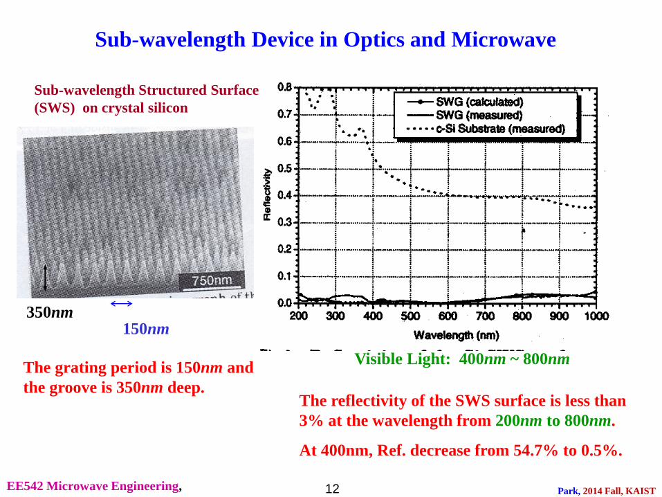
Sub-wavelength Structured Surfaces
(SWS) on crystal silicon
Sub-wavelength Device in Optics and Microwave
350nm
Visible Light: 400nm ~ 800nm The grating period is 150nm and
the groove is 350nm deep.
150nm
The reflectivity of the SWS surface is less than
3% at the wavelength from 200nm to 800nm.
At 400nm, Ref. decrease from 54.7% to 0.5%.
EE542 Microwave Engineering, Park, 2013. Fall, KAIST Park, 2014 Fall, KAIST

S.-O. Park, KAIST 13
Manufacturing Photonic Materials: The Biological Option
As yet, technology has not caught up with our desire to create fully three dimensional, micron scale,
periodic structures. Drawing patterns on a surface presents few problems to the integrated circuit industry,
but that third dimension defeats us for the time being; though not, we suspect, for long.
On the other hand nearly all of biology is `engineered' on the
micron scale and with the help of DNA very complex structures
are manufactured. Not surprisingly the optical properties are
frequently exploited, nowhere with more spectacular effect than in
the butterfly. Many species show irridescent green or blue
patches and these owe their colouring to diffraction from periodic
material in the scales of the wing. On the left is an electron
micrograph of a broken scale taken from mitoura grynea
revealing a periodic array of holes responsible for the colour.
Right we see a specimen of the Adonis Blue
butterfly. Note the blue patches to the rear
of the wing.
EE542 Microwave Engineering, Park, 2013. Fall, KAIST Park, 2014 Fall, KAIST
S.-O. Park, KAIST 14 ICE649 Microwave Engineering,
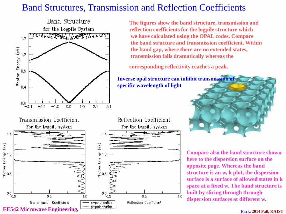
Band Structures, Transmission and Reflection Coefficients
The figures show the band structure, transmission and
reflection coefficients for the logpile structure which
we have calculated using the OPAL codes. Compare
the band structure and transmission coefficient. Within
the band gap, where there are no extended states,
transmission falls dramatically whereas the
corresponding reflectivity reaches a peak.
Compare also the band structure shown
here to the dispersion surface on the
opposite page. Whereas the band
structure is an w, k plot, the dispersion
surface is a surface of allowed states in k
space at a fixed w. The band structure is
built by slicing through through
dispersion surfaces at different w.
Inverse opal structure can inhibit transmission of
specific wavelength of light
EE542 Microwave Engineering, Park, 2013. Fall, KAIST Park, 2014 Fall, KAIST

S.-O. Park, KAIST 15
Transmission Parameters V Incident
Transmission Coefficient = T =
V Transmitted
V Incident
= t
DUT
Gain (dB) = 20 Log V
Trans
V Inc
= 20 log t
Insertion Phase (deg) = V
Trans
V Inc
=
Transmission coefficient T is defined as the transmitted voltage divided by the incident voltage. If
|Vtrans| > |Vinc|, we have gain, and if |Vtrans| < |Vinc|, we have attenuation or insertion loss. When
insertion loss is expressed in dB, a negative sign is added in the definition so that the loss value is
expressed as a positive number. The phase portion of the transmission coefficient is called insertion
phase.
Looking at insertion phase directly is usually not very useful. This is because the phase has a large
negative slope with respect to frequency due to the electrical length of the device (the longer the device,
the greater the slope). Often, the electrical delay feature of the network analyzer is used to remove the
linear portion of the phase response. This has the effect of removing the electrical length of the DUT,
resulting in a high-resolution display showing any deviations from linear phase.
Insertion Loss (dB) = - 20 Log V
Trans
V Inc
= - 20 log t
V Transmitted
EE542 Microwave Engineering, Park, 2013. Fall, KAIST Park, 2014 Fall, KAIST
S.-O. Park, KAIST 16
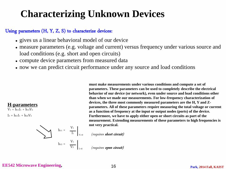
Characterizing Unknown Devices
Using parameters (H, Y, Z, S) to characterize devices: gives us a linear behavioral model of our device
measure parameters (e.g. voltage and current) versus frequency under various source and
load conditions (e.g. short and open circuits)
compute device parameters from measured data
now we can predict circuit performance under any source and load conditions
H-parameters V1 = h11I1 + h12V2
I2 = h21I1 + h22V2
h11 = V1
I1 V2=0
h12 = V1
V2 I1=0
(requires short circuit)
(requires open circuit)
must make measurements under various conditions and compute a set of
parameters. These parameters can be used to completely describe the electrical
behavior of our device (or network), even under source and load conditions other
than when we made our measurements. For low-frequency characterization of
devices, the three most commonly measured parameters are the H, Y and Z-
parameters. All of these parameters require measuring the total voltage or current
as a function of frequency at the input or output nodes (ports) of the device.
Furthermore, we have to apply either open or short circuits as part of the
measurement. Extending measurements of these parameters to high frequencies is
not very practical.
EE542 Microwave Engineering, Park, 2013. Fall, KAIST Park, 2014 Fall, KAIST

S.-O. Park, KAIST 17
Why Use S-Parameters?
relatively easy to obtain at high frequencies
measure voltage traveling waves with a vector
network analyzer
don't need shorts/opens which can cause active
devices to oscillate or self-destruct
relate to familiar measurement (gain,
loss, reflection coefficient ...)
can cascade S-parameters of multiple
devices to predict system performance
can compute H, Y, or Z parameters
from S-parameters if desired
can easily import and use S-parameter files in our
electronic-simulation tools
Incident Transmitted S 21
S 11 Reflected S 22
Reflected
Transmitted Incident
b 1
a 1 b 2
a 2 S 12
DUT
b 1 = S 11 a 1 + S 12 a 2
b 2 = S 21 a 1 + S 22 a 2
Port 1 Port 2
EE542 Microwave Engineering, Park, 2013. Fall, KAIST Park, 2014 Fall, KAIST

S.-O. Park, KAIST 18
Measuring S-Parameters
S 11 = Reflected
Incident =
b 1
a 1 a 2 = 0
S 21 = Transmitted
Incident =
b 2
a 1 a 2 = 0
S 22 = Reflected
Incident =
b 2
a 2 a 1 = 0
S 12 = Transmitted
Incident =
b 1
a 2 a 1 = 0
Incident Transmitted S 21
S 11
Reflected b 1
a 1
b 2
Z 0
Load
a 2 = 0
DUT Forward
1
Incident Transmitted S 12
S 22
Reflected
b 2
a 2
b
a 1 = 0
DUT Z 0
Load Reverse
EE542 Microwave Engineering, Park, 2013. Fall, KAIST Park, 2014 Fall, KAIST

S.-O. Park, KAIST 19
Equating S-Parameters with Common Measurement
Terms
S11 = forward reflection coefficient (input match)
S22 = reverse reflection coefficient (output match)
S21 = forward transmission coefficient (gain or loss)
S12 = reverse transmission coefficient (isolation)
Remember, S-parameters are inherently linear quantities -- however,
we often express them in a log-magnitude format
S-parameters are essentially the same parameters as some of the terms we have
mentioned before, as described above. Remember, S-parameters are inherently linear
quantities -- however, we often express them in a log-magnitude format. S11 and S22 are
often displayed on a Smith chart.
EE542 Microwave Engineering, Park, 2013. Fall, KAIST Park, 2014 Fall, KAIST

S.-O. Park, KAIST 20
Early Days of Radar Chain Home Radar, Deployment Began 1936
Dover
Radar Site

S.-O. Park, KAIST 21
Frequency : 20-30 MHz
• Wavelength
10-15 m
• Antenna
- Dipole Array on Transmit
- Crossed Dipoles on Receive
• Azimuth Beamwidth
- about 100 degree
• Peak Power
- 350 kW
• Detection Range
~160 nmi on
German Bomber
Chain Home Radar Antenna System

S.-O. Park, KAIST 22
What Means are Available for Lifting the Fog of War ?
S.-O. Park, KAIST 23
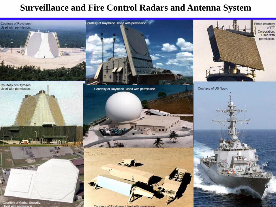
Surveillance and Fire Control Radars and Antenna System

S.-O. Park, KAIST 24
Sources of Noise Received by Antenna
S.-O. Park, KAIST 25 < 01 / 20 >
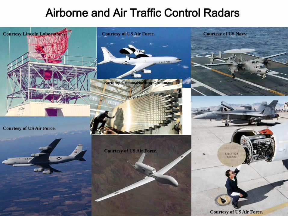
Courtesy Lincoln Laboratory.
Courtesy of US Air Force.
Northrop GrummaNorthropGrumman
Courtesy of US Navy.
Courtesy of US Air Force.
Courtesy of US Air Force.
Courtesy of US Air Force.
Airborne and Air Traffic Control Radars
S.-O. Park, KAIST 26 < 01 / 20 >
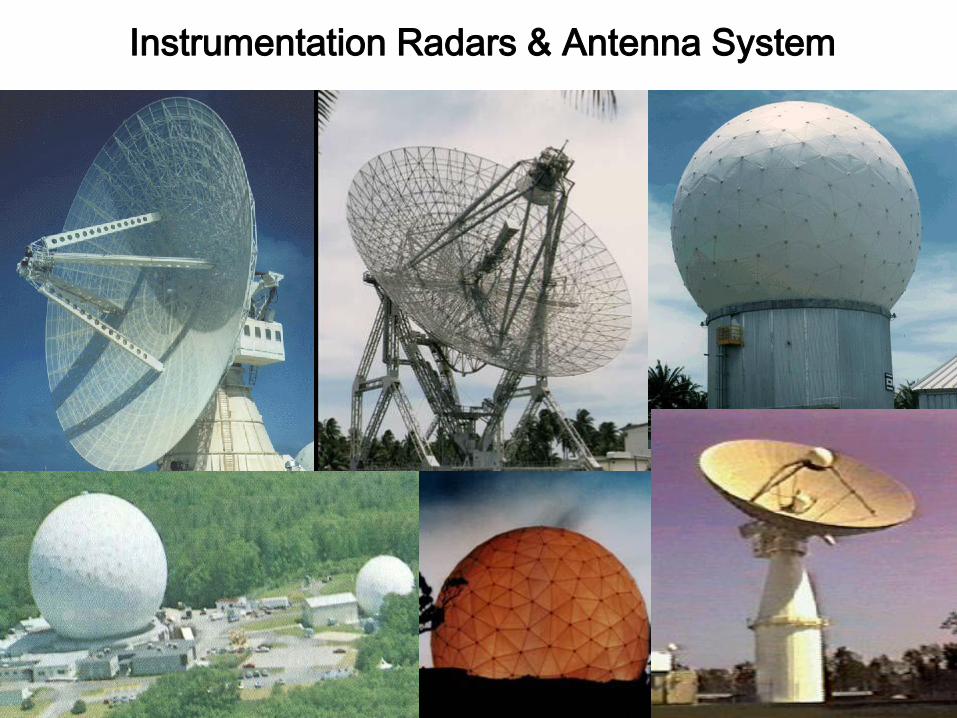
Instrumentation Radars & Antenna System

S.-O. Park, KAIST 27
SPY-1
4100
elements
Large Phased Arrays Antenna System
THAAD Radar
25,344 elements
Courtesy of Raytheon.
Used with permission. Cobra Dane
15.3K active elements

S.-O. Park, KAIST 28
Synthetic Aperture Radar
Synthetic aperture radar technology has provided terrain structural information to geologists for mineral
exploration, oil spill boundaries on water to environmentalists, sea state and ice hazard maps to navigators,
and reconnaissance and targeting information to military operations. There are many other applications or
potential applications. Some of these, particularly civilian, have not yet been adequately explored because
lower cost electronics are just beginning to make SAR technology economical for smaller scale uses.
Interferometry (3-D SAR).
Aa a part of the Airborne Multisensor Pod System
(AMPS) program, Sandia operates and maintains
the SAR pod. The SAR operates in the Ku-band
and is capable of 1 meter resolution. The pod is
visible under the right wing (near the fuselage) of
the aircraft.
S.-O. Park, KAIST 29
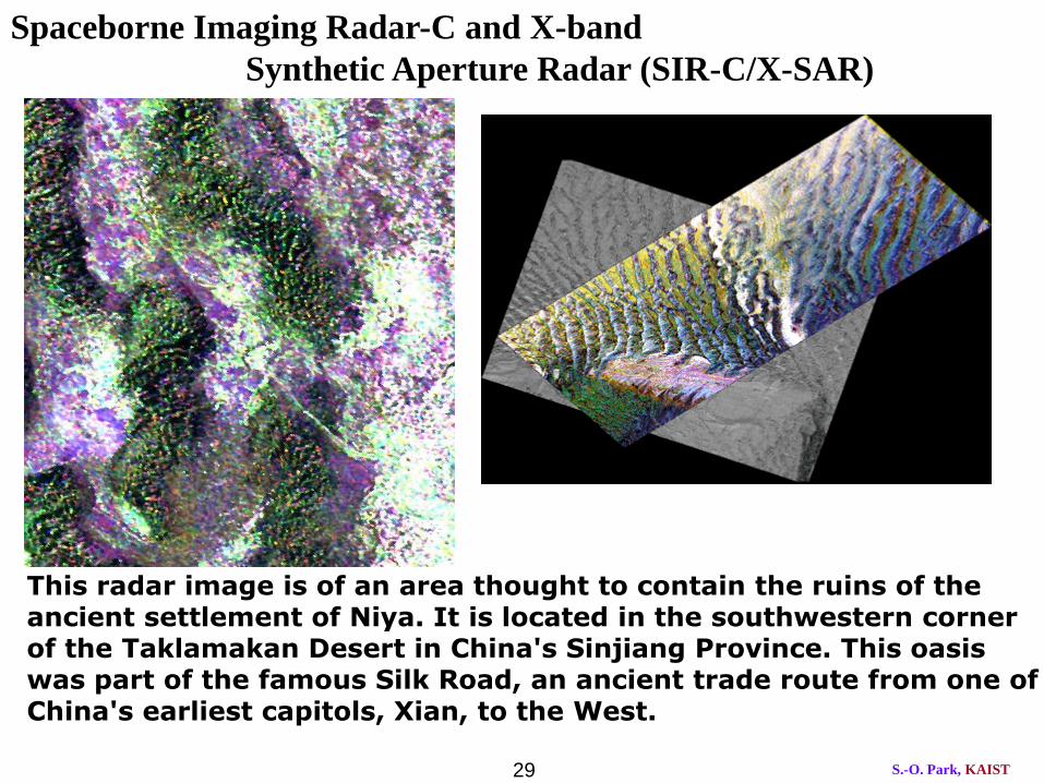
This radar image is of an area thought to contain the ruins of the ancient settlement of Niya. It is located in the southwestern corner of the Taklamakan Desert in China's Sinjiang Province. This oasis was part of the famous Silk Road, an ancient trade route from one of China's earliest capitols, Xian, to the West.
Spaceborne Imaging Radar-C and X-band
Synthetic Aperture Radar (SIR-C/X-SAR)
S.-O. Park, KAIST 30
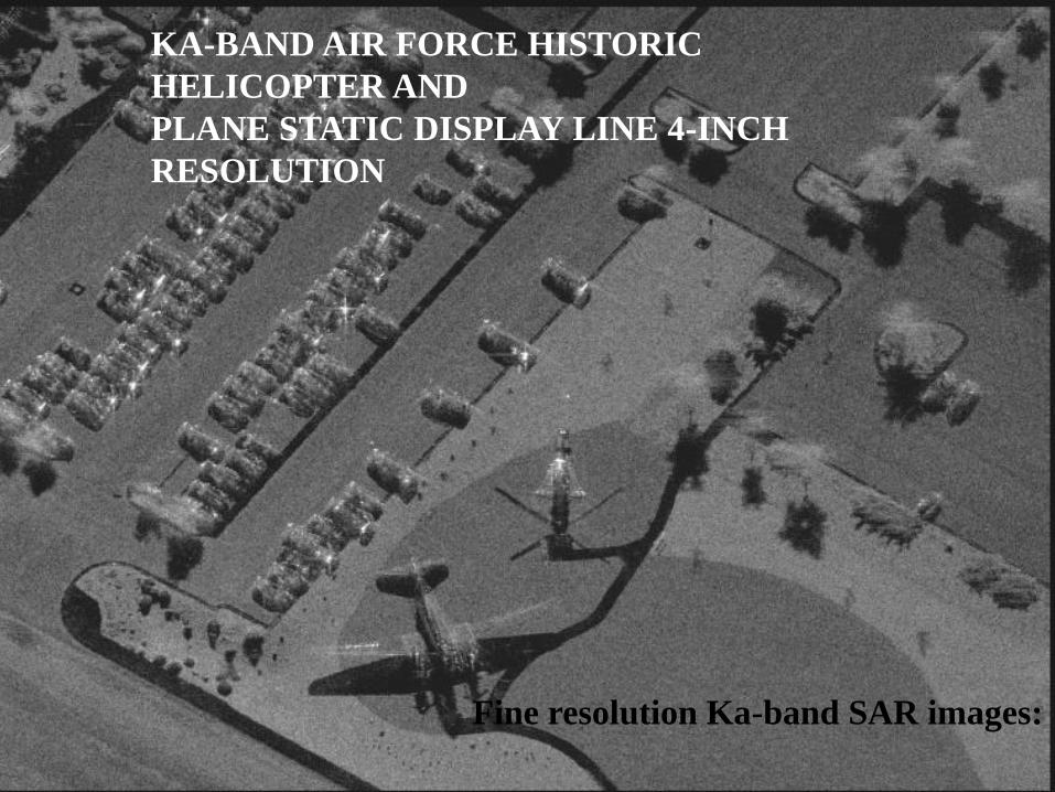
KA-BAND AIR FORCE HISTORIC
HELICOPTER AND
PLANE STATIC DISPLAY LINE 4-INCH
RESOLUTION
Fine resolution Ka-band SAR images:

S.-O. Park, KAIST 31
KA-BAND C-130s ON FLIGHT LINE 4-INCH RESOLUTION
fine resolution Ka-band SAR images:
S.-O. Park, KAIST 32
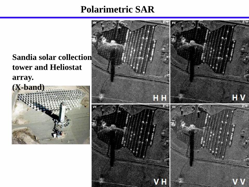
Sandia solar collection
tower and Heliostat
array.
(X-band)
Polarimetric SAR

S.-O. Park, KAIST 33
Predator UAV
–High-resolution Ku-band spotlight SAR: 0.1m
resolution
–Stripmap SAR at arbitrary angles: 0.3m resolution
–Exoclutter Moving Target Indicator (MTI)
–Near-real-time coherent-change detection (CCD)
–Extended range operation: 33 km with 4 mm/hr rain
or 55 km without rain at 0.3-m resolution
–Low weight and power: 119-lb total weight, < 1.2-kW
prime power
General Atomic’s AN/APY-8 Lynx Radar in production
Predator UAV