EE25266 ASIC/FPGA Chip Design - Sharif University...
13
EE25266 – ASIC/FPGA Chip Design Mahdi Shabany Electrical Engineering Department Sharif University of Technology Assignment #8 Designing a FIR Filter, FPGA in the Loop, Ethernet Introduction In this lab, you are shown one way of specifying, simulating, and implementing a FIR filter using the System Generator’s FIR and FDATool blocks. The FDATool block is used to define the filter order and coefficients, and the FIR block is used for the Simulink simulation and design implementation in FPGA using Xilinx ISE. You are also able to verify the functionality of the design by running it through the actual hardware. Objectives After completing this lab, you will be able to: • Enter your filter characteristics and generate coefficients using the FDATool block • Simulate a design using the FIR block with the coefficients generated by the FDATool block • Perform hardware-in-the-loop verification Design Description You are DSP Designer in a company. Your company is investigating using Digital Filters instead of analog for its Security Tag detectors in an attempt to improve performance and reduce cost of the overall system. This will enable the company to further penetrate the growing security market space. The specification of the single channel, single rate filter is specified below: • Sampling Frequency (Fs) = 1.5 MHz • Fstop 1 = 270 KHz ● Fpass 1 = 300 KHz ● Fpass 2 = 450 Khz ● Fstop 2 = 480 KHz ● Attenuation on both sides of the passband = 54 dB ● Pass band ripple = 1 The company has chosen to go with FPGAs due to their flexibility and time to market and performance advantages over DSP Processors. Your HDL design experience is limited and hence
Transcript of EE25266 ASIC/FPGA Chip Design - Sharif University...
EE25266 – ASIC/FPGA Chip Design
Mahdi Shabany Electrical Engineering Department
Sharif University of Technology
Assignment #8
Designing a FIR Filter, FPGA in the Loop, Ethernet
Introduction In this lab, you are shown one way of specifying, simulating, and implementing a FIR filter using the System Generator’s FIR and FDATool blocks. The FDATool block is used to define the filter order and coefficients, and the FIR block is used for the Simulink simulation and design implementation in FPGA using Xilinx ISE. You are also able to verify the functionality of the design by running it through the actual hardware.
Objectives After completing this lab, you will be able to: • Enter your filter characteristics and generate coefficients using the FDATool block • Simulate a design using the FIR block with the coefficients generated by the FDATool block • Perform hardware-in-the-loop verification
Design Description You are DSP Designer in a company. Your company is investigating using Digital Filters instead of analog for its Security Tag detectors in an attempt to improve performance and reduce cost of the overall system. This will enable the company to further penetrate the growing security market space. The specification of the single channel, single rate filter is specified below: • Sampling Frequency (Fs) = 1.5 MHz • Fstop 1 = 270 KHz ● Fpass 1 = 300 KHz ● Fpass 2 = 450 Khz ● Fstop 2 = 480 KHz ● Attenuation on both sides of the passband = 54 dB ● Pass band ripple = 1 The company has chosen to go with FPGAs due to their flexibility and time to market and performance advantages over DSP Processors. Your HDL design experience is limited and hence
System Generator for DSP appears to be an excellent solution for implementing the filter in an FPGA, as you are already familiar with The MathWorks products. Your manager has requested that you create a prototype of the filter to be implemented on their Atlys board prototype board that is almost complete. The prototype must be finished as quickly as possible for the imminent Aggressive Security convention, which is the industry’s largest convention of the year, so it must not be missed. Your manager has provided a starting model that includes input sources and output sink. Your design must be simulated using a Random Source and the chirp from the DSP Blockset. To analyze the output of the filter, input and output signals are displayed in a spectrum scope. A spectrum scope is used to compare the frequency response of the fixed-point FIR filter, which will be implemented in the FPGA. Two different sources are used to simulate the filter: • The chirp block, which sweeps between the specified frequencies of 0 to 750kHz • The random source generator, which outputs a random signal of uniform distribution with a range of 0 to 1 Uniform is a better choice to drive a fixed-point filter because it is bounded.
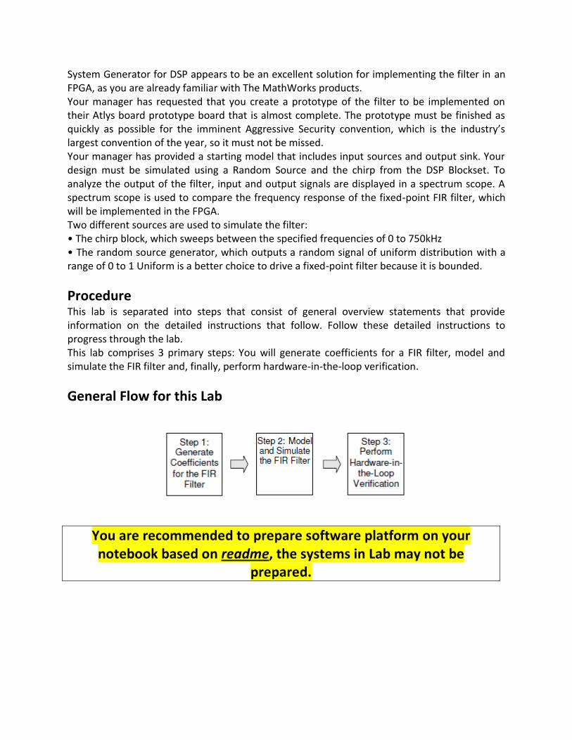
Procedure This lab is separated into steps that consist of general overview statements that provide information on the detailed instructions that follow. Follow these detailed instructions to progress through the lab. This lab comprises 3 primary steps: You will generate coefficients for a FIR filter, model and simulate the FIR filter and, finally, perform hardware-in-the-loop verification.
General Flow for this Lab
You are recommended to prepare software platform on your notebook based on readme, the systems in Lab may not be
prepared.
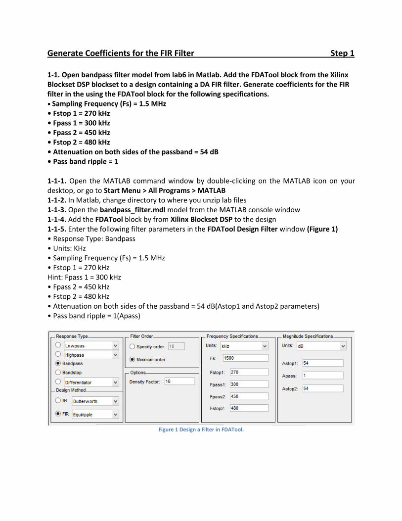
Generate Coefficients for the FIR Filter Step 1 1-1. Open bandpass filter model from lab6 in Matlab. Add the FDATool block from the Xilinx Blockset DSP blockset to a design containing a DA FIR filter. Generate coefficients for the FIR filter in the using the FDATool block for the following specifications. • Sampling Frequency (Fs) = 1.5 MHz • Fstop 1 = 270 kHz • Fpass 1 = 300 kHz • Fpass 2 = 450 kHz • Fstop 2 = 480 kHz • Attenuation on both sides of the passband = 54 dB • Pass band ripple = 1 1-1-1. Open the MATLAB command window by double-clicking on the MATLAB icon on your desktop, or go to Start Menu > All Programs > MATLAB 1-1-2. In Matlab, change directory to where you unzip lab files 1-1-3. Open the bandpass_filter.mdl model from the MATLAB console window 1-1-4. Add the FDATool block by from Xilinx Blockset DSP to the design 1-1-5. Enter the following filter parameters in the FDATool Design Filter window (Figure 1) • Response Type: Bandpass • Units: KHz • Sampling Frequency (Fs) = 1.5 MHz • Fstop 1 = 270 kHz Hint: Fpass 1 = 300 kHz • Fpass 2 = 450 kHz • Fstop 2 = 480 kHz • Attenuation on both sides of the passband = 54 dB(Astop1 and Astop2 parameters) • Pass band ripple = 1(Apass)
Figure 1 Design a Filter in FDATool.
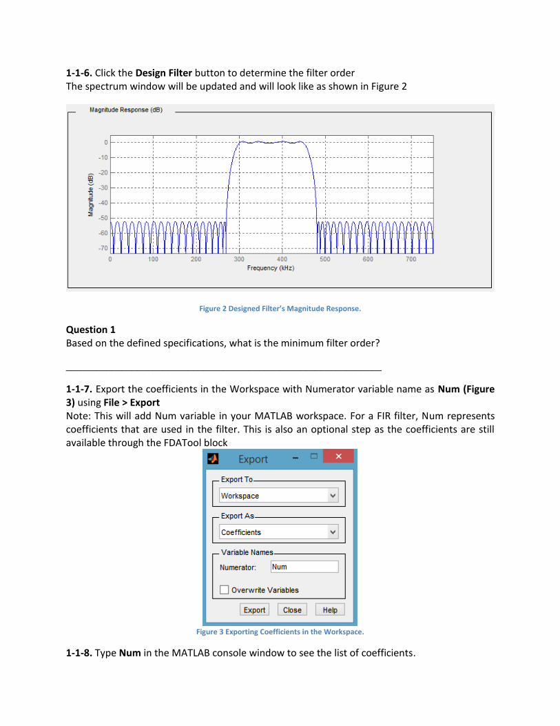
1-1-6. Click the Design Filter button to determine the filter order The spectrum window will be updated and will look like as shown in Figure 2
Figure 2 Designed Filter’s Magnitude Response.
Question 1 Based on the defined specifications, what is the minimum filter order?
______________________________________________________________
1-1-7. Export the coefficients in the Workspace with Numerator variable name as Num (Figure 3) using File > Export Note: This will add Num variable in your MATLAB workspace. For a FIR filter, Num represents coefficients that are used in the filter. This is also an optional step as the coefficients are still available through the FDATool block
Figure 3 Exporting Coefficients in the Workspace.
1-1-8. Type Num in the MATLAB console window to see the list of coefficients.
1-1-9. Type max(Num) and min(Num) in the MATLAB console window to determine the maximum coefficient value that adequately specifies the coefficient width and binary point Question 2 Fill in following information related to the coefficients Maximum value: _______________________________________ Minimum value: _______________________________________
Model and Simulate the FIR Filter Step 2
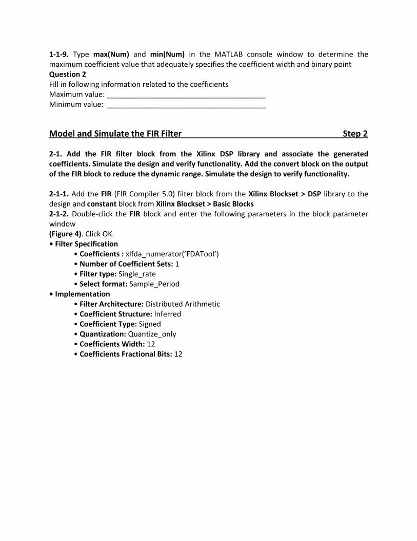
2-1. Add the FIR filter block from the Xilinx DSP library and associate the generated coefficients. Simulate the design and verify functionality. Add the convert block on the output of the FIR block to reduce the dynamic range. Simulate the design to verify functionality. 2-1-1. Add the FIR (FIR Compiler 5.0) filter block from the Xilinx Blockset > DSP library to the design and constant block from Xilinx Blockset > Basic Blocks 2-1-2. Double-click the FIR block and enter the following parameters in the block parameter window (Figure 4). Click OK. • Filter Specification
• Coefficients : xlfda_numerator(’FDATool’) • Number of Coefficient Sets: 1 • Filter type: Single_rate • Select format: Sample_Period
• Implementation • Filter Architecture: Distributed Arithmetic • Coefficient Structure: Inferred • Coefficient Type: Signed • Quantization: Quantize_only • Coefficients Width: 12 • Coefficients Fractional Bits: 12
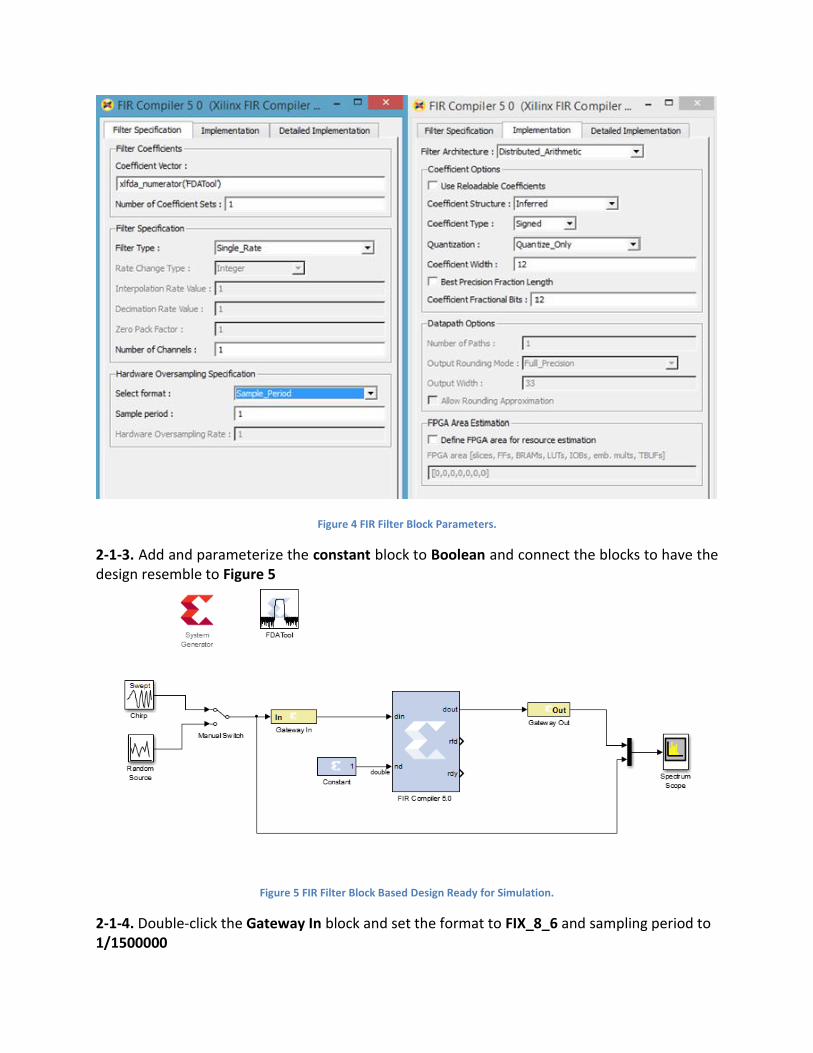
Figure 4 FIR Filter Block Parameters.
2-1-3. Add and parameterize the constant block to Boolean and connect the blocks to have the design resemble to Figure 5
Figure 5 FIR Filter Block Based Design Ready for Simulation.
2-1-4. Double-click the Gateway In block and set the format to FIX_8_6 and sampling period to 1/1500000
2-1-5. Select the Chirp Source and start the simulation 2-1-6. Bring the scope to the front and verify that the signal coming out of the FIR filter has been attenuated and they look like Figure 6 and Figure 7, below.
Figure 6 Attenuation in Passband (Spectrum Scope).
Figure 7 Attenuation in Stopband (Spectrum Scope).
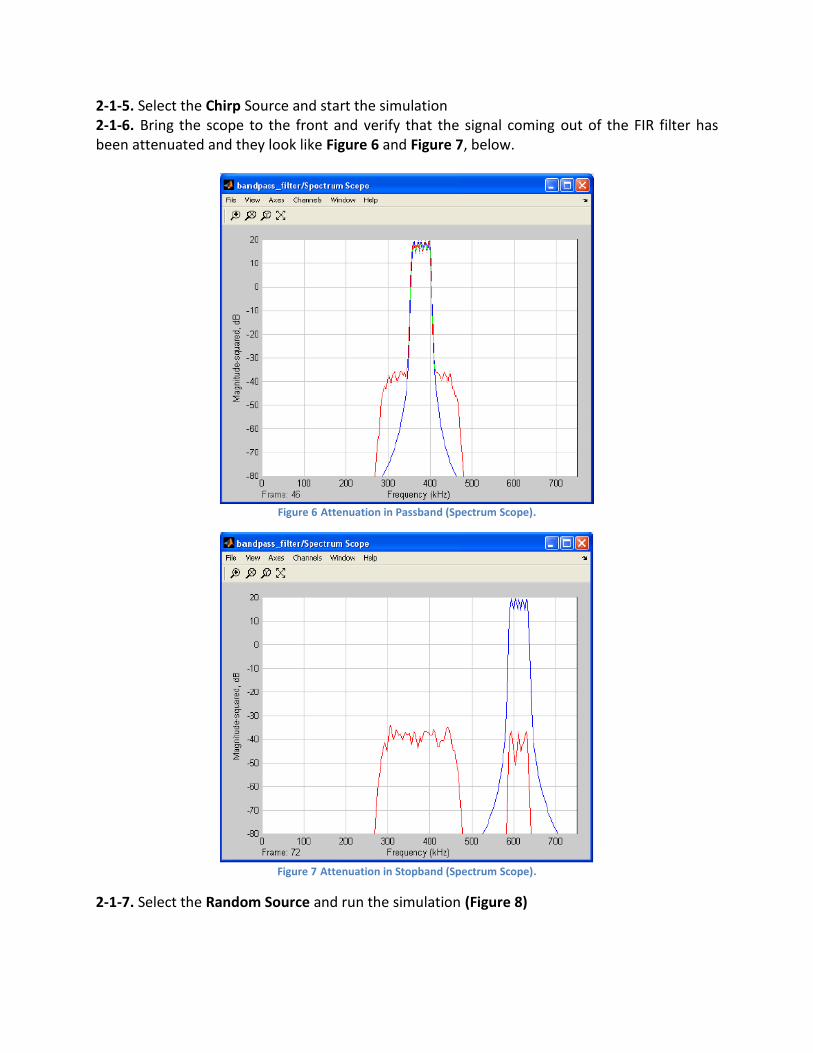
2-1-7. Select the Random Source and run the simulation (Figure 8)
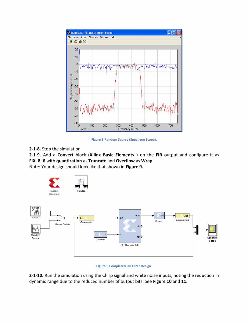
Figure 8 Random Source (Spectrum Scope).
2-1-8. Stop the simulation 2-1-9. Add a Convert block (Xilinx Basic Elements ) on the FIR output and configure it as FIX_8_6 with quantization as Truncate and Overflow as Wrap Note: Your design should look like that shown in Figure 9.
Figure 9 Completed FIR Filter Design.
2-1-10. Run the simulation using the Chirp signal and white noise inputs, noting the reduction in dynamic range due to the reduced number of output bits. See Figure 10 and 11.
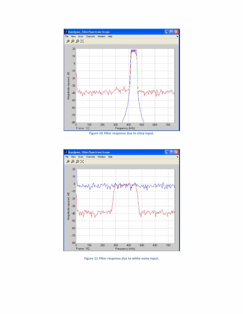
Figure 10 Filter response due to chirp input.
Figure 11 Filter response due to white noise input.
Perform Hardware-in-the-Loop Verification Step 3
3-1. Using the System Generator token, generate the hardware and verify that the design works through the hardware board. Simulate the design through Simulink. 3-1-1. Save the model as bandpass_filter_hw.mdl 3-1-2. Double-click the System Generator token and set the following parameters In Compilation Window ● Compilation: Hardware Co-Simulation Atlys JTAG
• Synthesis Tool: XST • Target Directory: ./lab/hwcosim (or ./hwcosim) • Create Testbench: Unchecked • Create Interface document : Unchecked
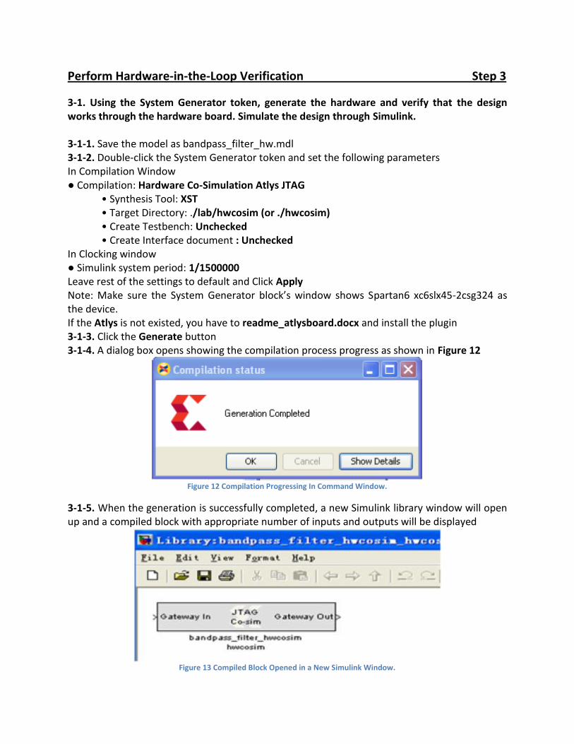
In Clocking window ● Simulink system period: 1/1500000 Leave rest of the settings to default and Click Apply Note: Make sure the System Generator block’s window shows Spartan6 xc6slx45-2csg324 as the device. If the Atlys is not existed, you have to readme_atlysboard.docx and install the plugin 3-1-3. Click the Generate button 3-1-4. A dialog box opens showing the compilation process progress as shown in Figure 12
Figure 12 Compilation Progressing In Command Window.
3-1-5. When the generation is successfully completed, a new Simulink library window will open up and a compiled block with appropriate number of inputs and outputs will be displayed
Figure 13 Compiled Block Opened in a New Simulink Window.
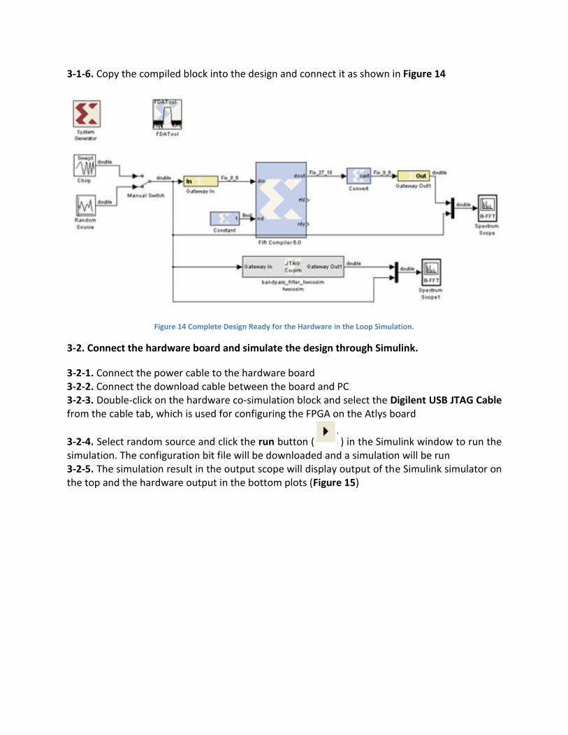
3-1-6. Copy the compiled block into the design and connect it as shown in Figure 14
Figure 14 Complete Design Ready for the Hardware in the Loop Simulation.
3-2. Connect the hardware board and simulate the design through Simulink.
3-2-1. Connect the power cable to the hardware board 3-2-2. Connect the download cable between the board and PC 3-2-3. Double-click on the hardware co-simulation block and select the Digilent USB JTAG Cable from the cable tab, which is used for configuring the FPGA on the Atlys board
3-2-4. Select random source and click the run button ( ) in the Simulink window to run the simulation. The configuration bit file will be downloaded and a simulation will be run 3-2-5. The simulation result in the output scope will display output of the Simulink simulator on the top and the hardware output in the bottom plots (Figure 15)
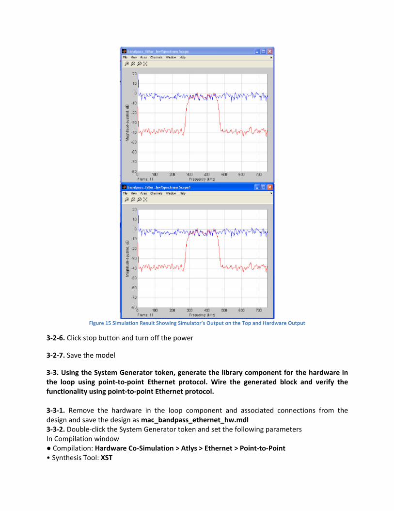
Figure 15 Simulation Result Showing Simulator’s Output on the Top and Hardware Output
3-2-6. Click stop button and turn off the power
3-2-7. Save the model
3-3. Using the System Generator token, generate the library component for the hardware in the loop using point-to-point Ethernet protocol. Wire the generated block and verify the functionality using point-to-point Ethernet protocol. 3-3-1. Remove the hardware in the loop component and associated connections from the design and save the design as mac_bandpass_ethernet_hw.mdl 3-3-2. Double-click the System Generator token and set the following parameters In Compilation window ● Compilation: Hardware Co-Simulation > Atlys > Ethernet > Point-to-Point • Synthesis Tool: XST
• Create Testbench: Unchecked • Target Directory: ./lab/hwcosim_eth (or ./hwcosim_eth) • Create Interface Document: Unchecked In Clocking window ● Simulink sytem period: 1/1500000 Leave rest of the settings to default and click Apply Note: Make sure the System Generator block’s window shows Spartan6 xc6slx45-2csg324 as the part. If Atlys is not shown, then refer readme_atlysboard.docx and install the plugin
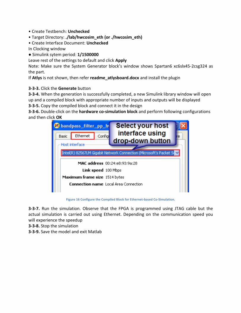
3-3-3. Click the Generate button 3-3-4. When the generation is successfully completed, a new Simulink library window will open up and a compiled block with appropriate number of inputs and outputs will be displayed 3-3-5. Copy the compiled block and connect it in the design 3-3-6. Double-click on the hardware co-simulation block and perform following configurations and then click OK
Figure 16 Configure the Compiled Block for Ethernet-based Co-Simulation.
3-3-7. Run the simulation. Observe that the FPGA is programmed using JTAG cable but the actual simulation is carried out using Ethernet. Depending on the communication speed you will experience the speedup 3-3-8. Stop the simulation 3-3-9. Save the model and exit Matlab