
EE25266 ASIC/FPGA Chip Design - Sharif University...
16
EE25266 – ASIC/FPGA Chip Design Mahdi Shabany Electrical Engineering Department Sharif University of Technology Assignment #7 Getting started with Atlys board and ISE design environment Part I ) In pervious assignments you got familiar with Quartus software and how to use it to Synthesis a Verilog code , set some constraint and pin assignments , do place and route and map it to one of Altera’s FPGAs , generate bit-stream and finally load it to the target FPGA (Most of these steps take place sequentially when you press run -a purple triangle- on Quartus) . ISE is Quartus counterpart for Xilinx’s (one other famous FPGA developer company) FPGAs. Xilinx ISE also is an integrated software which makes it possible for user to implement a digital design on a Xilinx’s FPGA from A to Z. In this part we are getting started with ISE through making a simple project. To run ISE, click on icon on your Lab computer’s desktop. To make a new project, select: File>New Project…, then New Project Wizard will open and help you to create a new project.
Transcript of EE25266 ASIC/FPGA Chip Design - Sharif University...

EE25266 – ASIC/FPGA Chip Design
Mahdi Shabany Electrical Engineering Department
Sharif University of Technology
Assignment #7
Getting started with Atlys board and ISE design environment
Part I ) In pervious assignments you got familiar with Quartus software and how to use it to
Synthesis a Verilog code , set some constraint and pin assignments , do place and route and
map it to one of Altera’s FPGAs , generate bit-stream and finally load it to the target FPGA
(Most of these steps take place sequentially when you press run -a purple triangle- on
Quartus) . ISE is Quartus counterpart for Xilinx’s (one other famous FPGA developer company)
FPGAs. Xilinx ISE also is an integrated software which makes it possible for user to implement a
digital design on a Xilinx’s FPGA from A to Z. In this part we are getting started with ISE through
making a simple project.
To run ISE, click on icon on your Lab computer’s desktop. To make a new project, select:
File>New Project…, then New Project Wizard will open and help you to create a new project.
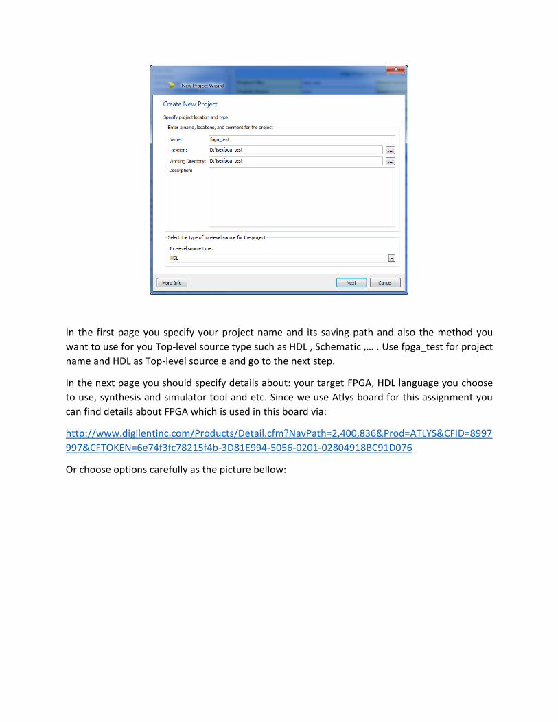
In the first page you specify your project name and its saving path and also the method you
want to use for you Top-level source type such as HDL , Schematic ,… . Use fpga_test for project
name and HDL as Top-level source e and go to the next step.
In the next page you should specify details about: your target FPGA, HDL language you choose
to use, synthesis and simulator tool and etc. Since we use Atlys board for this assignment you
can find details about FPGA which is used in this board via:
http://www.digilentinc.com/Products/Detail.cfm?NavPath=2,400,836&Prod=ATLYS&CFID=8997
997&CFTOKEN=6e74f3fc78215f4b-3D81E994-5056-0201-02804918BC91D076
Or choose options carefully as the picture bellow:
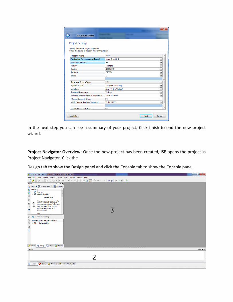
In the next step you can see a summary of your project. Click finish to end the new project
wizard.
Project Navigator Overview: Once the new project has been created, ISE opens the project in
Project Navigator. Click the
Design tab to show the Design panel and click the Console tab to show the Console panel.
1
2
3
The Design panel (1) contains two windows: a Sources window that displays all source files
associated with the current design and a Process window that displays all available processes
that can be run on a selected source file. The Console panel (2) displays status messages
including error and warning messages. The HDL editor window (3) displays source code from
files selected in the Design panel.
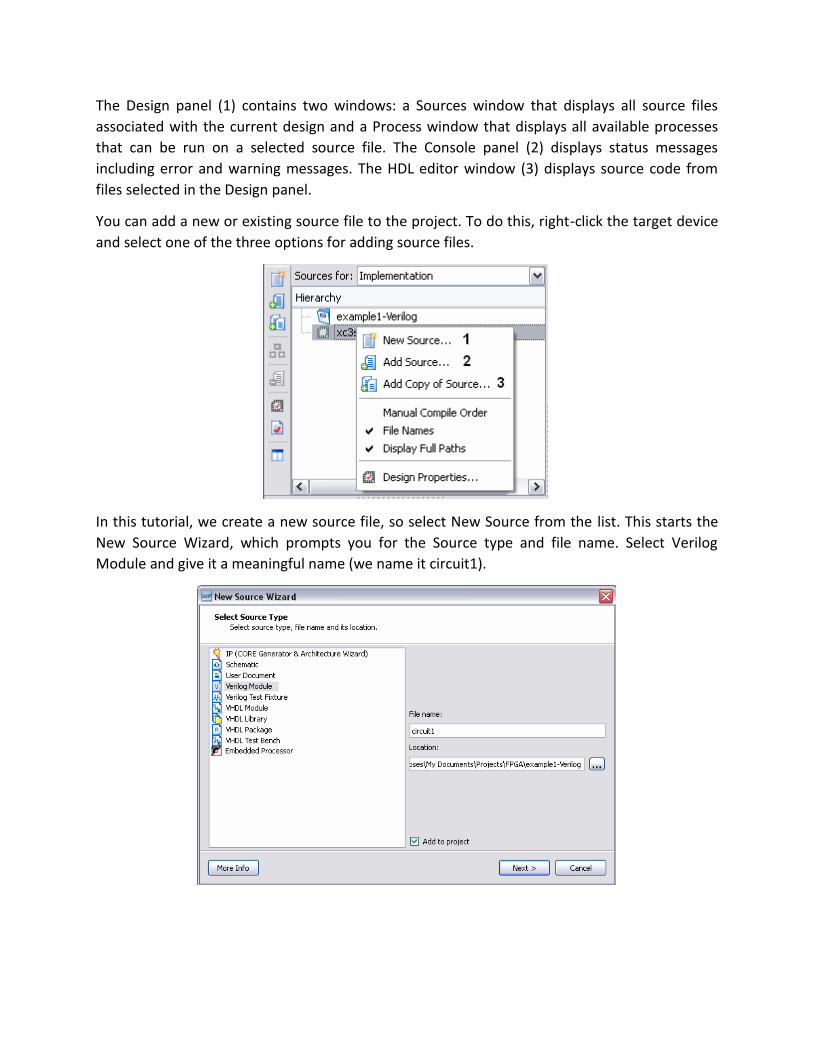
You can add a new or existing source file to the project. To do this, right-click the target device
and select one of the three options for adding source files.
In this tutorial, we create a new source file, so select New Source from the list. This starts the
New Source Wizard, which prompts you for the Source type and file name. Select Verilog
Module and give it a meaningful name (we name it circuit1).
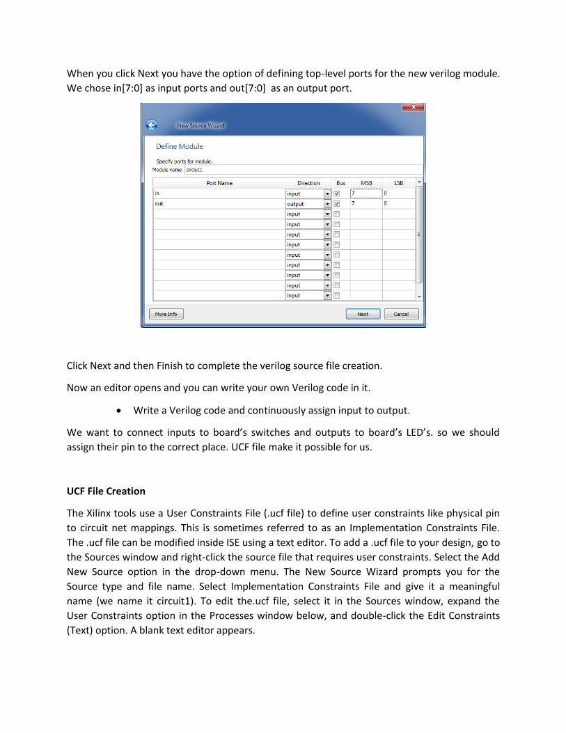
When you click Next you have the option of defining top-level ports for the new verilog module.
We chose in[7:0] as input ports and out[7:0] as an output port.
Click Next and then Finish to complete the verilog source file creation.
Now an editor opens and you can write your own Verilog code in it.
Write a Verilog code and continuously assign input to output.
We want to connect inputs to board’s switches and outputs to board’s LED’s. so we should
assign their pin to the correct place. UCF file make it possible for us.
UCF File Creation
The Xilinx tools use a User Constraints File (.ucf file) to define user constraints like physical pin
to circuit net mappings. This is sometimes referred to as an Implementation Constraints File.
The .ucf file can be modified inside ISE using a text editor. To add a .ucf file to your design, go to
the Sources window and right-click the source file that requires user constraints. Select the Add
New Source option in the drop-down menu. The New Source Wizard prompts you for the
Source type and file name. Select Implementation Constraints File and give it a meaningful
name (we name it circuit1). To edit the.ucf file, select it in the Sources window, expand the
User Constraints option in the Processes window below, and double-click the Edit Constraints
(Text) option. A blank text editor appears.
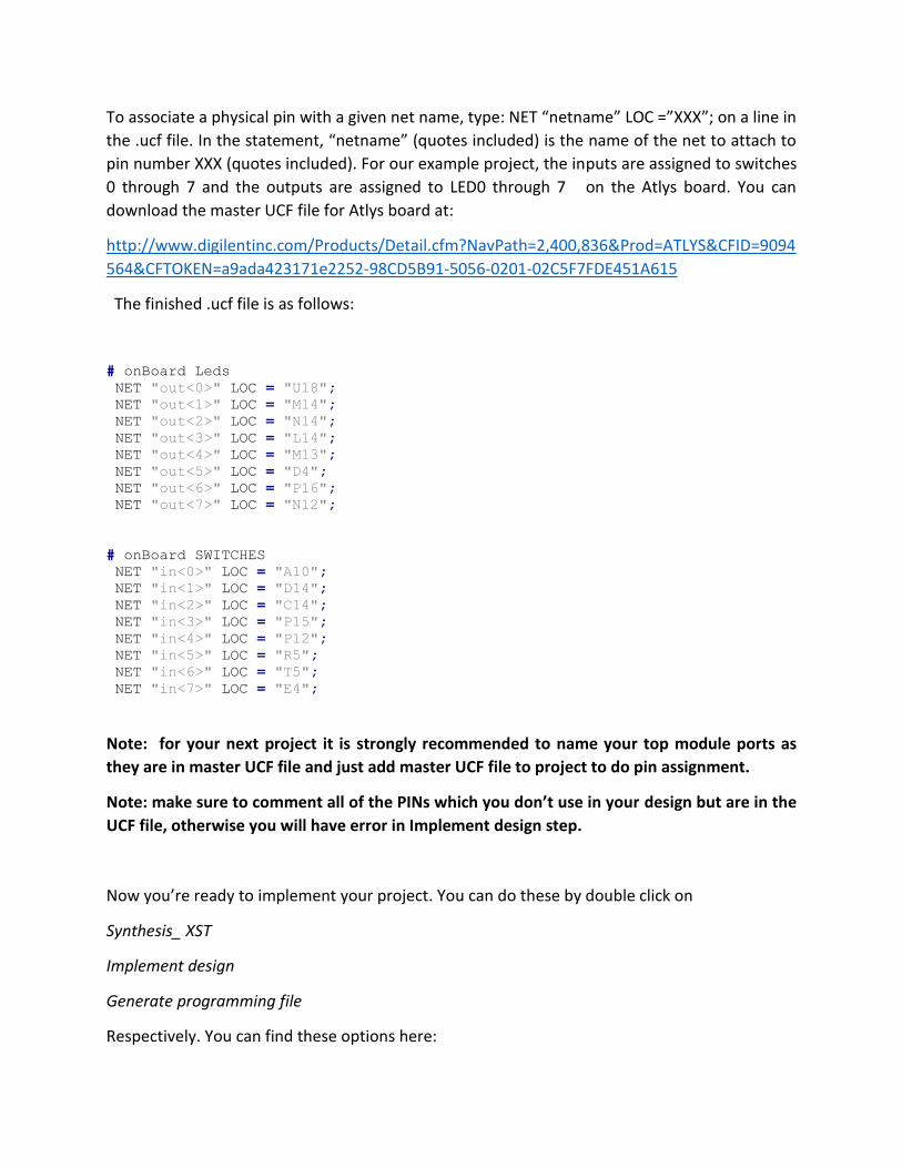
To associate a physical pin with a given net name, type: NET “netname” LOC =”XXX”; on a line in
the .ucf file. In the statement, “netname” (quotes included) is the name of the net to attach to
pin number XXX (quotes included). For our example project, the inputs are assigned to switches
0 through 7 and the outputs are assigned to LED0 through 7 on the Atlys board. You can
download the master UCF file for Atlys board at:
http://www.digilentinc.com/Products/Detail.cfm?NavPath=2,400,836&Prod=ATLYS&CFID=9094
564&CFTOKEN=a9ada423171e2252-98CD5B91-5056-0201-02C5F7FDE451A615
The finished .ucf file is as follows:
# onBoard Leds
NET "out<0>" LOC = "U18";
NET "out<1>" LOC = "M14";
NET "out<2>" LOC = "N14";
NET "out<3>" LOC = "L14";
NET "out<4>" LOC = "M13";
NET "out<5>" LOC = "D4";
NET "out<6>" LOC = "P16";
NET "out<7>" LOC = "N12";
# onBoard SWITCHES
NET "in<0>" LOC = "A10";
NET "in<1>" LOC = "D14";
NET "in<2>" LOC = "C14";
NET "in<3>" LOC = "P15";
NET "in<4>" LOC = "P12";
NET "in<5>" LOC = "R5";
NET "in<6>" LOC = "T5";
NET "in<7>" LOC = "E4";
Note: for your next project it is strongly recommended to name your top module ports as
they are in master UCF file and just add master UCF file to project to do pin assignment.
Note: make sure to comment all of the PINs which you don’t use in your design but are in the
UCF file, otherwise you will have error in Implement design step.
Now you’re ready to implement your project. You can do these by double click on
Synthesis_ XST
Implement design
Generate programming file
Respectively. You can find these options here:
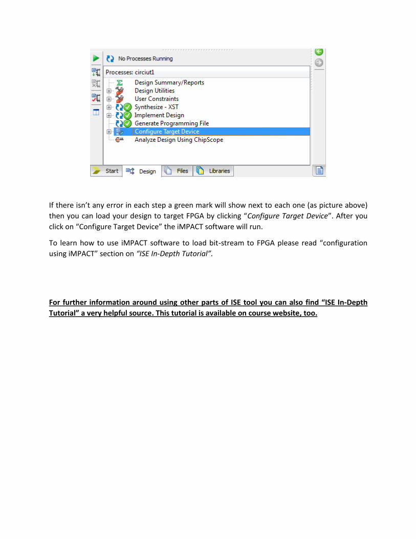
If there isn’t any error in each step a green mark will show next to each one (as picture above)
then you can load your design to target FPGA by clicking “Configure Target Device”. After you
click on “Configure Target Device” the iMPACT software will run.
To learn how to use iMPACT software to load bit-stream to FPGA please read “configuration
using iMPACT” section on “ISE In-Depth Tutorial”.
For further information around using other parts of ISE tool you can also find “ISE In-Depth
Tutorial” a very helpful source. This tutorial is available on course website, too.

Part II) using Core Generator to implement a Block RAM controller.
In this part first you are supposed to synthesis a memory as a Block Ram to store your student number.
This Block Ram will be like a table of digits which should be dynamic. You should move in the table and
read any digits from the memory or rewrite a digit in the memory block. To do that, you will have four
control buttons: Up, Down, Write and Sum.
Up: to go from the current address to the previous address.
For example when the address pointer points to “0” in the table and the Up button is pushed, the
address pointer moves from “0” to the address for digit “2” in the table.
New Address
Previous Address
*Note: moving starts from the first digit of your student ID.
Down: to go from the previous address to the current address.
Previous Address
New Address
9
1
2
0
3
7
5
5
9
1
2
0
3
7
5
5
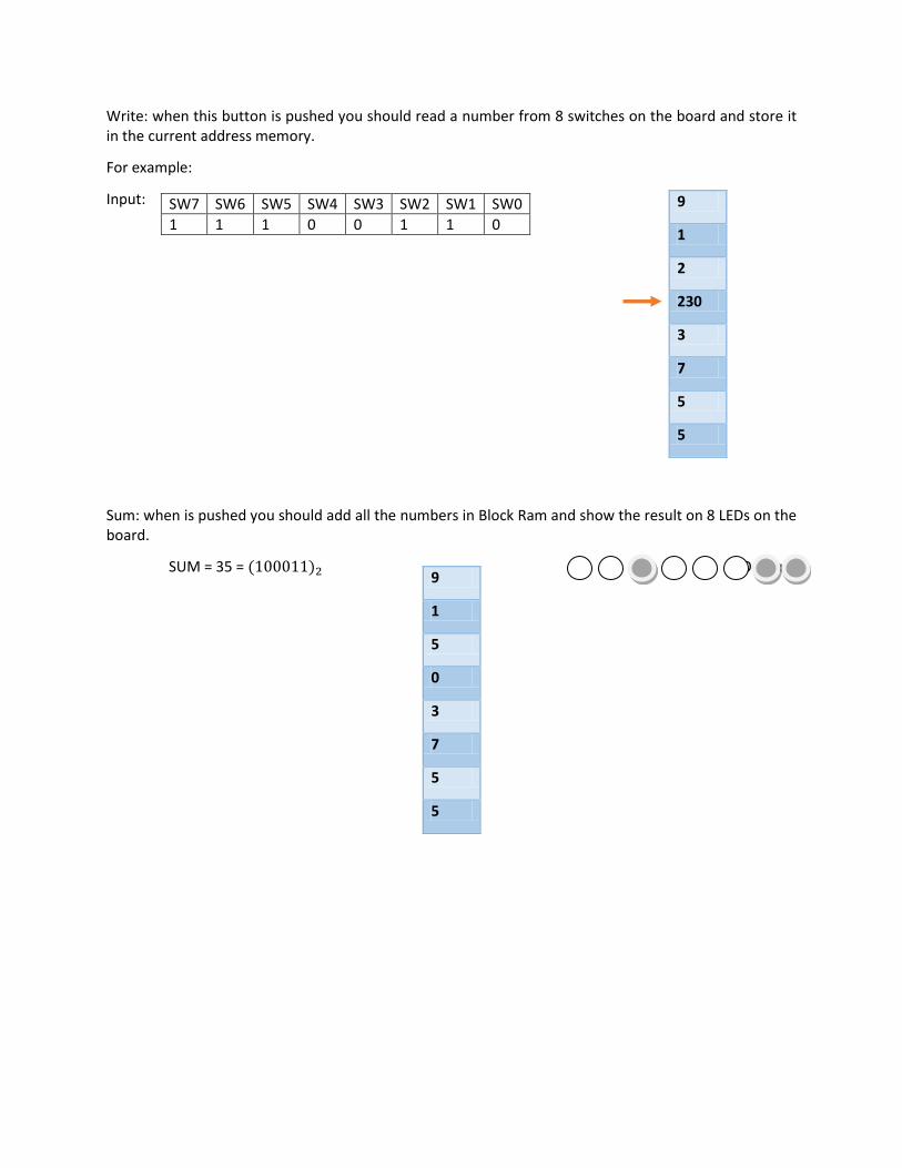
Write: when this button is pushed you should read a number from 8 switches on the board and store it in the current address memory.
For example:
Input:
Sum: when is pushed you should add all the numbers in Block Ram and show the result on 8 LEDs on the board.
SUM = 35 = Output:
SW7 SW6 SW5 SW4 SW3 SW2 SW1 SW0
1 1 1 0 0 1 1 0
9
1
2
230
3
7
5
5
9
1
5
0
3
7
5
5
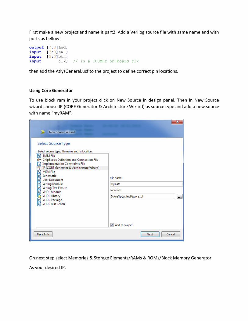
First make a new project and name it part2. Add a Verilog source file with same name and with
ports as bellow:
output [7:0]Led;
input [7:0]sw ;
input [5:0]btn;
input clk; // is a 100MHz on-board clk
then add the AtlysGeneral.ucf to the project to define correct pin locations.
Using Core Generator
To use block ram in your project click on New Source in design panel. Then in New Source
wizard choose IP (CORE Generator & Architecture Wizard) as source type and add a new source
with name “myRAM”.
On next step select Memories & Storage Elements/RAMs & ROMs/Block Memory Generator
As your desired IP.
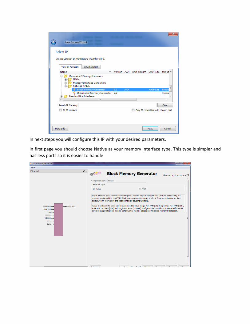
In next steps you will configure this IP with your desired parameters.
In first page you should choose Native as your memory interface type. This type is simpler and
has less ports so it is easier to handle
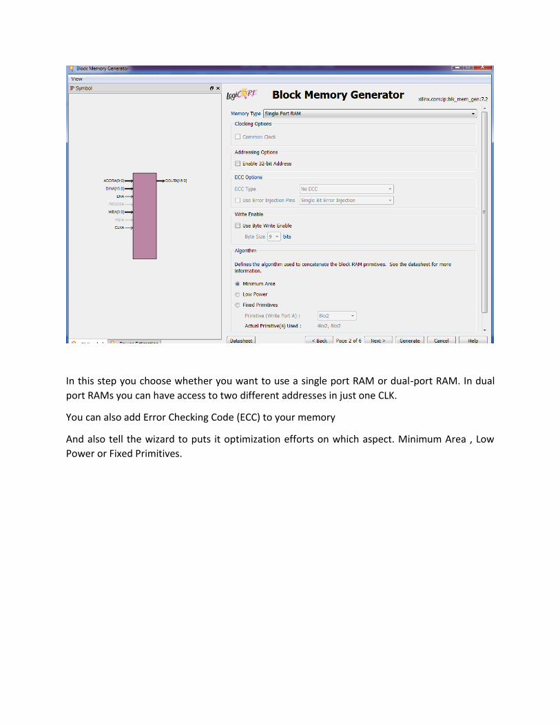
In this step you choose whether you want to use a single port RAM or dual-port RAM. In dual
port RAMs you can have access to two different addresses in just one CLK.
You can also add Error Checking Code (ECC) to your memory
And also tell the wizard to puts it optimization efforts on which aspect. Minimum Area , Low
Power or Fixed Primitives.
*
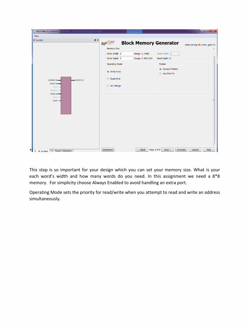
This step is so important for your design which you can set your memory size. What is your
each word’s width and how many words do you need. In this assignment we need a 8*8
memory. For simplicity choose Always Enabled to avoid handling an extra port.
Operating Mode sets the priority for read/write when you attempt to read and write an address
simultaneously.
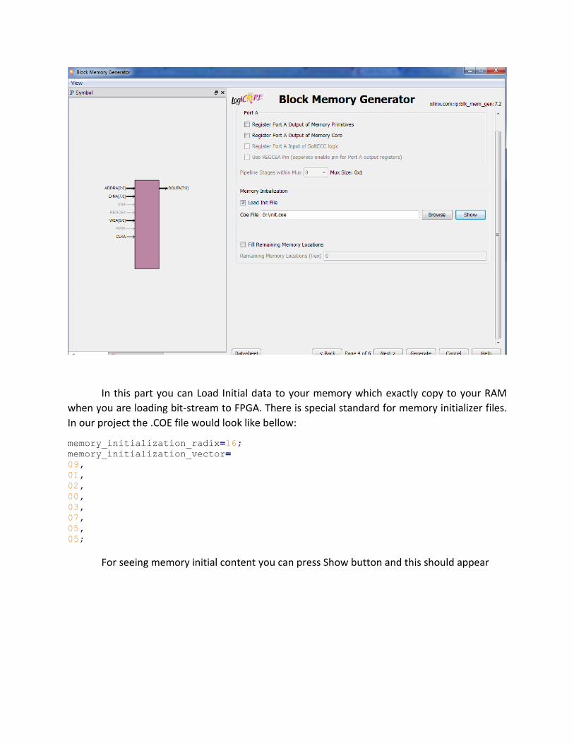
In this part you can Load Initial data to your memory which exactly copy to your RAM
when you are loading bit-stream to FPGA. There is special standard for memory initializer files.
In our project the .COE file would look like bellow:
memory_initialization_radix=16;
memory_initialization_vector=
09,
01,
02,
00,
03,
07,
05,
05;
For seeing memory initial content you can press Show button and this should appear
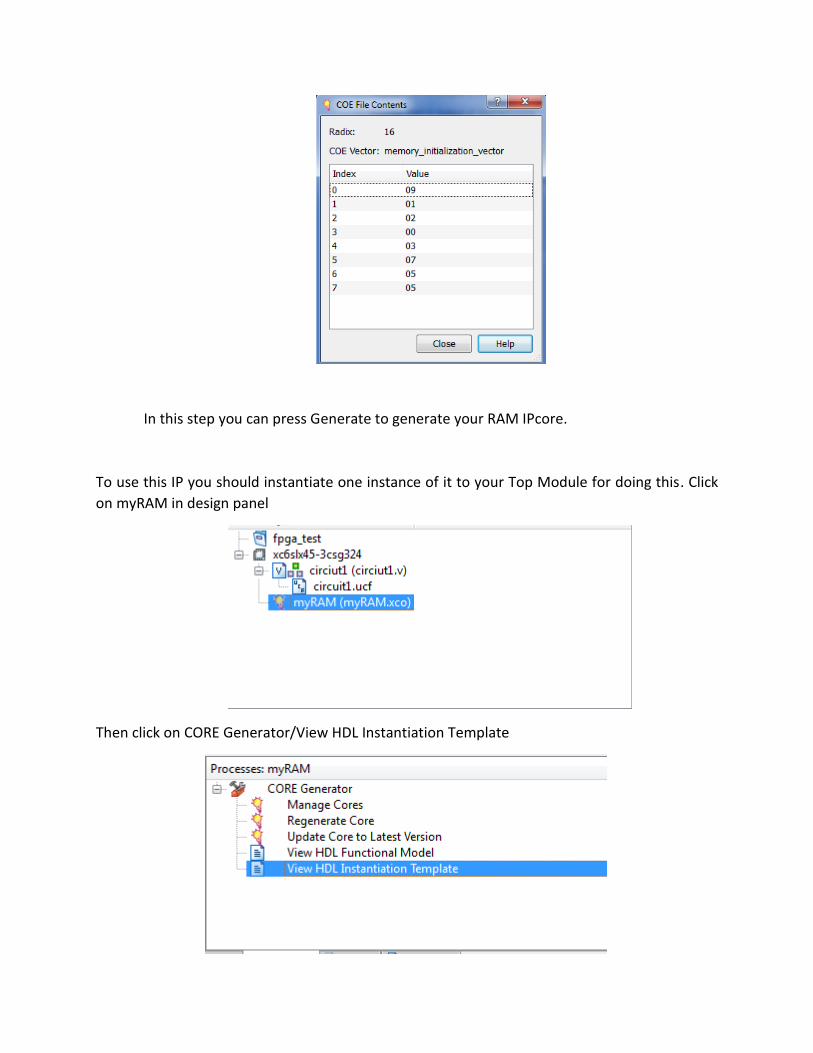
In this step you can press Generate to generate your RAM IPcore.
To use this IP you should instantiate one instance of it to your Top Module for doing this. Click
on myRAM in design panel
Then click on CORE Generator/View HDL Instantiation Template

You can use this template to instantiate RAM modules in your design.
Use this block RAM module and write a Verilog code to implement Part II
instructions.
Note : use buttons in this way :
Reset = ! btn [0] ;
Up = btn [1];
Down = btn [3] ;
Write= btn [4] ;
Sum = btn [5] ;