EE247 Lecture 20 - University of California, Berkeleyee247/fa08/files07/lectures/L20_f08.pdfEE247...
30
EECS 247- Lecture 20 Nyquist Rate ADCs © 2008 H.K. Page 1 EE247 Lecture 20 ADC Converters Comparator design • Single-stage open-loop amplifier • Cascade of open-loop amplifiers • Problem associated with DC offset – Cascaded output series cancellation – Input series cancellation – Offset cancellation through additional input pair plus offset storage capacitors • Latched comparators • Comparator examples EECS 247- Lecture 20 Nyquist Rate ADCs © 2008 H.K. Page 2 Voltage Comparators Play an important role in majority of ADCs Function: Compare the instantaneous value of two analog signals & generate a digital output voltage based on the sign of the difference: + - V out (Digital Output) V DD If V i+ -V i- > 0 V out =“1” If V i+ -V i- < 0 V out =“0” V i+ V i-
Transcript of EE247 Lecture 20 - University of California, Berkeleyee247/fa08/files07/lectures/L20_f08.pdfEE247...

EECS 247- Lecture 20 Nyquist Rate ADCs © 2008 H.K. Page 1
EE247Lecture 20
ADC ConvertersComparator design
• Single-stage open-loop amplifier• Cascade of open-loop amplifiers• Problem associated with DC offset
– Cascaded output series cancellation– Input series cancellation– Offset cancellation through additional input pair plus
offset storage capacitors• Latched comparators• Comparator examples
EECS 247- Lecture 20 Nyquist Rate ADCs © 2008 H.K. Page 2
Voltage Comparators
Play an important role in majority of ADCsFunction: Compare the instantaneous value of two analog signals &
generate a digital output voltage based on the sign of the difference:
+
-Vout (Digital Output)
VDD
If Vi+ -Vi- > 0 Vout=“1”If Vi+ -Vi- < 0 Vout=“0”
Vi+
Vi-
EECS 247- Lecture 20 Nyquist Rate ADCs © 2008 H.K. Page 3
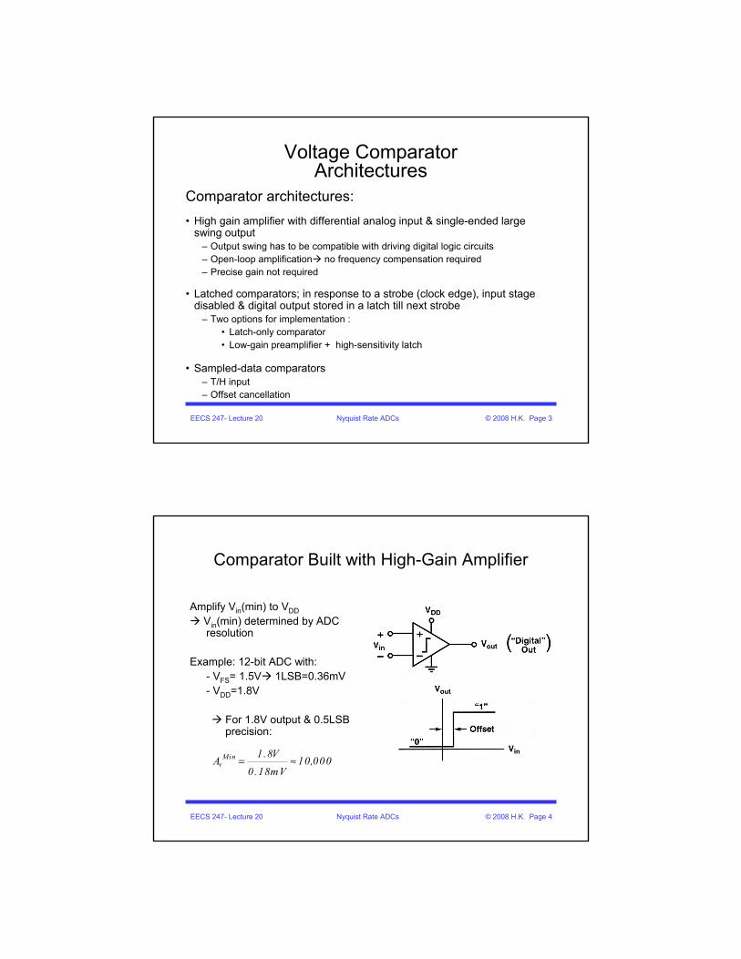
Voltage ComparatorArchitectures
Comparator architectures:• High gain amplifier with differential analog input & single-ended large
swing output– Output swing has to be compatible with driving digital logic circuits– Open-loop amplification no frequency compensation required– Precise gain not required
• Latched comparators; in response to a strobe (clock edge), input stage disabled & digital output stored in a latch till next strobe
– Two options for implementation :• Latch-only comparator• Low-gain preamplifier + high-sensitivity latch
• Sampled-data comparators– T/H input– Offset cancellation
EECS 247- Lecture 20 Nyquist Rate ADCs © 2008 H.K. Page 4
Comparator Built with High-Gain Amplifier
Amplify Vin(min) to VDD Vin(min) determined by ADC resolution
Example: 12-bit ADC with:- VFS= 1.5V 1LSB=0.36mV- VDD=1.8V
For 1.8V output & 0.5LSB precision:
Minv
1.8VA 10,000
0.18mV= ≈
EECS 247- Lecture 20 Nyquist Rate ADCs © 2008 H.K. Page 5
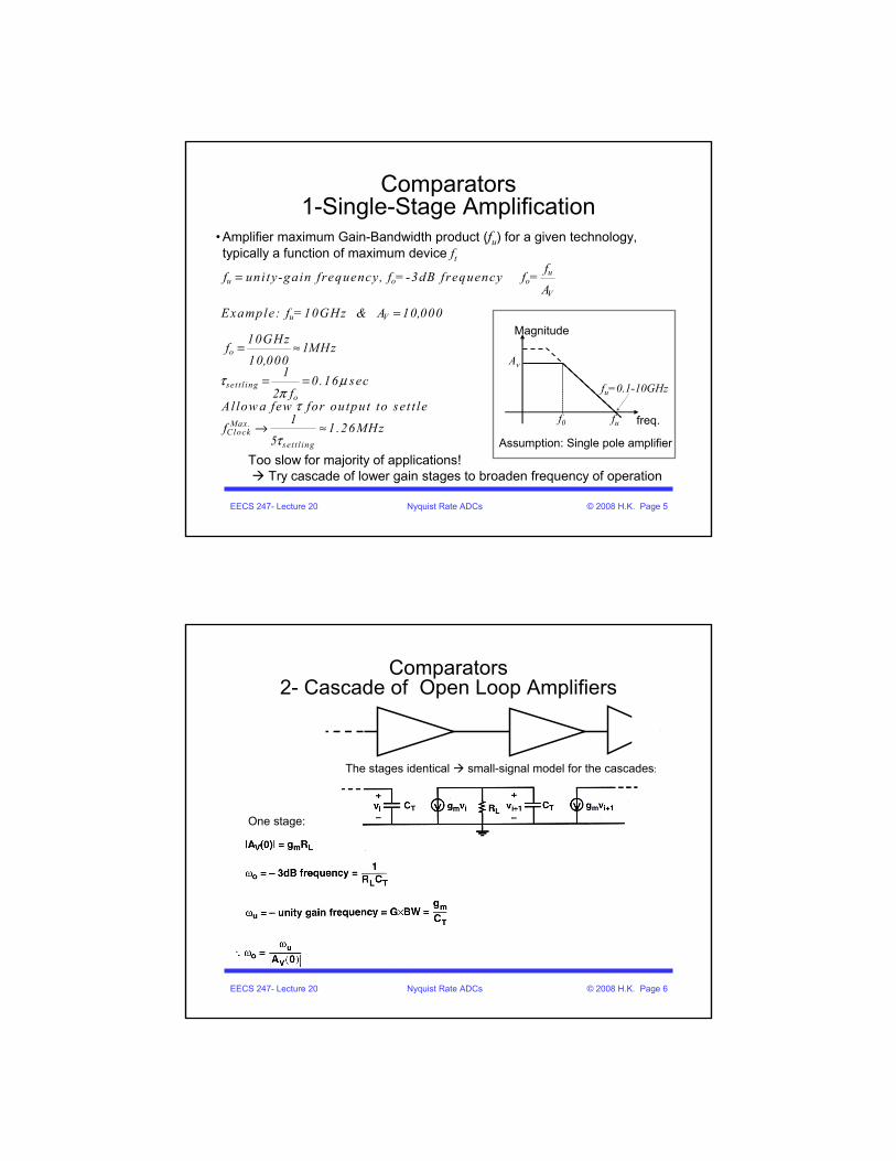
Comparators 1-Single-Stage Amplification
Too slow for majority of applications!Try cascade of lower gain stages to broaden frequency of operation
Assumption: Single pole amplifier
• Amplifier maximum Gain-Bandwidth product (fu) for a given technology, typically a function of maximum device ft
uu o o
V
u V
o
set t l ingo
Max.Clock
set t l ing
ff uni ty-gain frequency, f =-3dB frequency f =
A
Example: f =10GHz & A 10,000
10GHz f 1MHz
10,0001
0.16 sec2 f
Al low a few for output to set t le 1
f 1 .26MHz5
τ μπ
τ
τ
=
=
= ≈
= =
→ ≈
fu=0.1-10GHz
f0 fu freq.
Magnitude
Av
EECS 247- Lecture 20 Nyquist Rate ADCs © 2008 H.K. Page 6
Comparators2- Cascade of Open Loop Amplifiers
The stages identical small-signal model for the cascades:
One stage:
EECS 247- Lecture 20 Nyquist Rate ADCs © 2008 H.K. Page 7
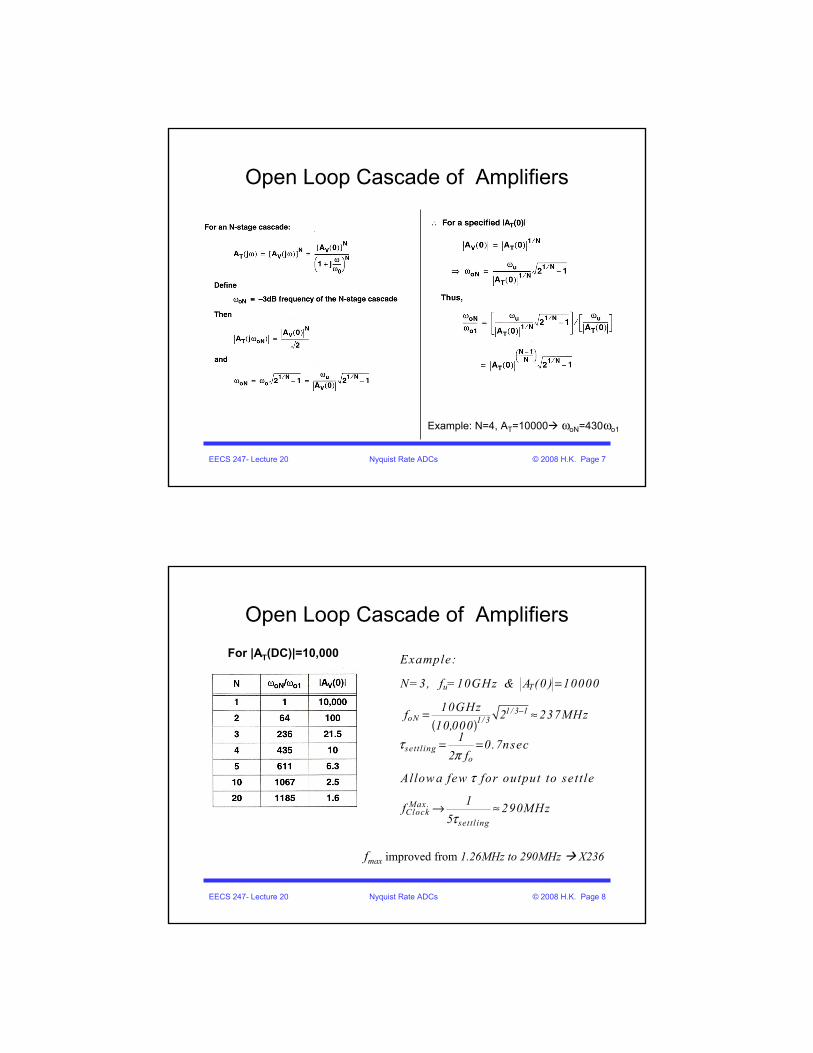
Open Loop Cascade of Amplifiers
Example: N=4, AT=10000 ωoN=430ωo1
EECS 247- Lecture 20 Nyquist Rate ADCs © 2008 H.K. Page 8
Open Loop Cascade of AmplifiersFor |AT(DC)|=10,000
( )
u T
1/ 3 1oN 1/ 3
settlingo
Max.Clock
settl ing
Example:
N=3, f =10GHz & A (0 ) 10000
10GHzf 2 237MHz10,000
1 0.7nsec2 f
Allow a few for output to settle
1f 290MHz5
τπ
τ
τ
−
=
= ≈
= =
→ ≈
fmax improved from 1.26MHz to 290MHz X236

EECS 247- Lecture 20 Nyquist Rate ADCs © 2008 H.K. Page 9
Open Loop Cascade of AmplifiersOffset Voltage
• From offset point of view: high gain/stage is preferred
• Choice of # of stage
bandwidth vs offset tradeoff
Input-referred offset
EECS 247- Lecture 20 Nyquist Rate ADCs © 2008 H.K. Page 10
Open Loop Cascade of AmplifiersStep Response
• Assuming linear behavior (not slew limited)
t

EECS 247- Lecture 20 Nyquist Rate ADCs © 2008 H.K. Page 11
Open Loop Cascade of AmplifiersStep Response
•Assuming linear behavior
EECS 247- Lecture 20 Nyquist Rate ADCs © 2008 H.K. Page 12
N 1 log A for A 1000opt 2 T
N 1.2ln A for A 1000opt T
≈ + <
≈ ≥
Open Loop Cascade of AmplifiersDelay/(C/gm)
• Minimum total delay broad function of N
• Relationship between # of stages resulting in minimize delay (Nop) and gain (Vout/Vin) approximately:
Delay/(C/gm)
Ref: J.T. Wu, et al., “A 100-MHz pipelined CMOS comparator ” IEEE Journal of Solid-State Circuits, vol. 23, pp. 1379 - 1385, December 1988.
( )1/ N
out
m inD
C VN !
g Vτ ⎡ ⎤⎛ ⎞ ⎛ ⎞
⎢ ⎥⎜ ⎟ ⎜ ⎟⎝ ⎠⎝ ⎠ ⎣ ⎦
=

EECS 247- Lecture 20 Nyquist Rate ADCs © 2008 H.K. Page 13
Offset Cancellation• In sampled-data cascade of amplifiers Vos can be cancelled
Store on ac-coupling caps in series with amp stages
• Offset associated with a specific amp can be cancelled by storing it in series with either the input or the output of thatstage
• Offset can be cancelled by adding a pair of auxiliary inputs to the amplifier and storing the offset on capacitors connected to the aux. inputs during offset cancellation phase
Ref: J.T. Wu, et al., “A 100-MHz pipelined CMOS comparator ” IEEE Journal of Solid-State Circuits, vol. 23, pp. 1379 - 1385, December 1988.
EECS 247- Lecture 20 Nyquist Rate ADCs © 2008 H.K. Page 14
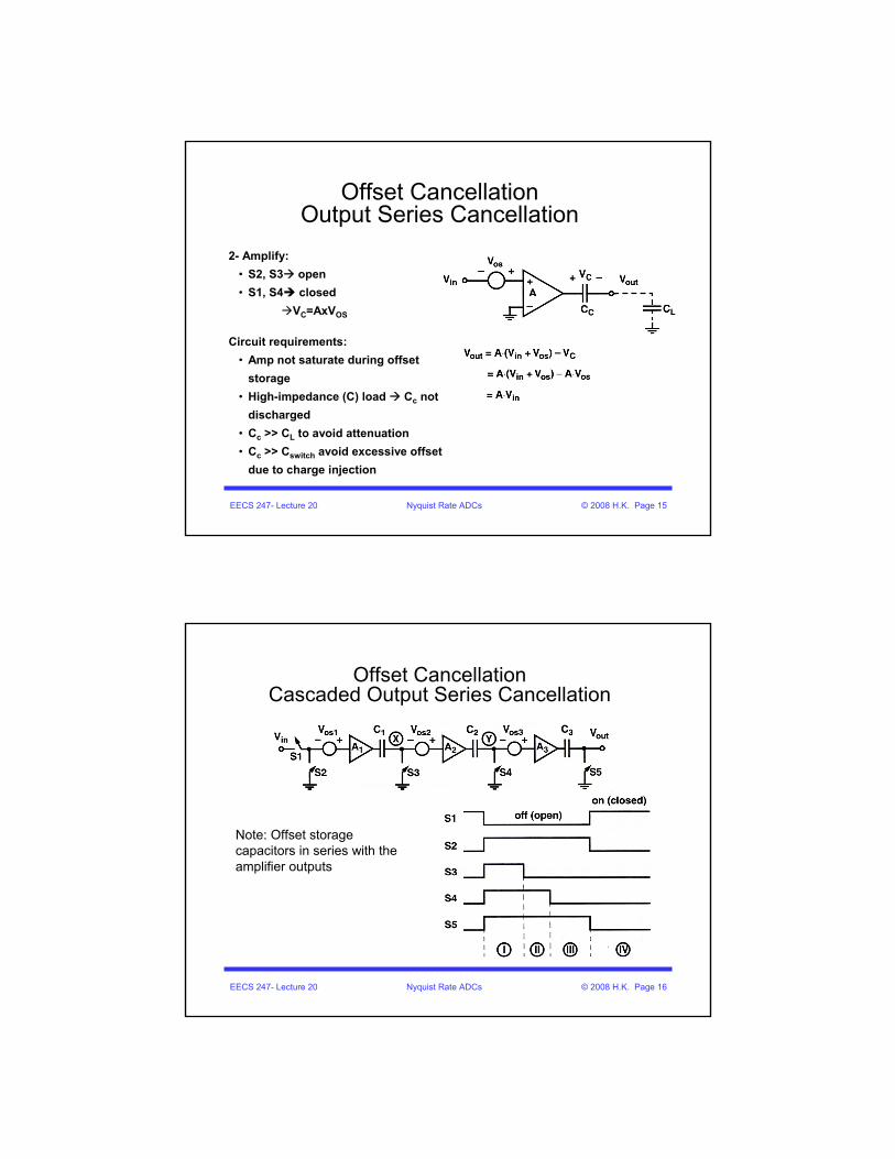
Offset CancellationOutput Series Cancellation
• Amp modeled as ideal + Vos (input referred)
1- Store offset:• S1, S4 open• S2, S3 closed
VC=AxVOS
Ref: J.T. Wu, et al., “A 100-MHz pipelined CMOS comparator ” IEEE Journal of Solid-State Circuits, vol. 23, pp. 1379 - 1385, December 1988.
EECS 247- Lecture 20 Nyquist Rate ADCs © 2008 H.K. Page 15
Offset CancellationOutput Series Cancellation
2- Amplify:• S2, S3 open• S1, S4 closed
VC=AxVOS
Circuit requirements:• Amp not saturate during offset
storage• High-impedance (C) load Cc not
discharged• Cc >> CL to avoid attenuation• Cc >> Cswitch avoid excessive offset
due to charge injection
EECS 247- Lecture 20 Nyquist Rate ADCs © 2008 H.K. Page 16
Offset CancellationCascaded Output Series Cancellation
Note: Offset storage capacitors in series with the amplifier outputs
EECS 247- Lecture 20 Nyquist Rate ADCs © 2008 H.K. Page 17
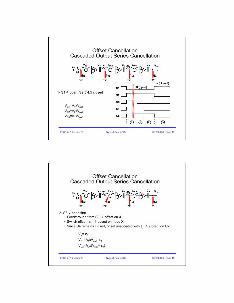
Offset CancellationCascaded Output Series Cancellation
1- S1 open, S2,3,4,5 closed
VC1=A1xVos1
VC2=A2xVos2
VC3=A1xVos3
EECS 247- Lecture 20 Nyquist Rate ADCs © 2008 H.K. Page 18
Offset CancellationCascaded Output Series Cancellation
2- S3 open first• Feedthrough from S3 offset on X• Switch offset , ε3 induced on node X• Since S4 remains closed, offset associated with ε3 stored on C2
VX= ε3
VC1=A1xVos1- ε3
VC2=A2x(Vos2+ ε3)
EECS 247- Lecture 20 Nyquist Rate ADCs © 2008 H.K. Page 19
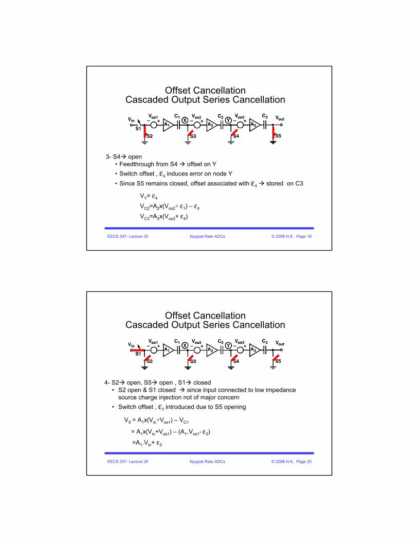
Offset CancellationCascaded Output Series Cancellation
3- S4 open• Feedthrough from S4 offset on Y• Switch offset , ε4 induces error on node Y• Since S5 remains closed, offset associated with ε4 stored on C3
VY= ε4
VC2=A2x(Vos2+ ε3) – ε4
VC3=A3x(Vos3+ ε4)
EECS 247- Lecture 20 Nyquist Rate ADCs © 2008 H.K. Page 20
Offset CancellationCascaded Output Series Cancellation
4- S2 open, S5 open , S1 closed• S2 open & S1 closed since input connected to low impedance
source charge injection not of major concern• Switch offset , ε5 introduced due to S5 opening
VX = A1x(Vin+Vos1) – VC1
= A1x(Vin+Vos1) – (A1.Vos1- ε3)
=A1.Vin+ ε3
EECS 247- Lecture 20 Nyquist Rate ADCs © 2008 H.K. Page 21
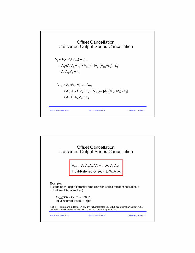
Offset CancellationCascaded Output Series Cancellation
Vy = A2x(Vx+Vos2) – VC2
= A2x(A1Vin + ε3 + Vos2) – [A2.(Vos2+ε3) - ε4]
=A1.A2.Vin + ε4
Vout = A3x(Vy+Vos3) – VC3
= A3.(A2xA1Vin + ε4 + Vos3) – [A3.(Vos3+ε4) - ε5]
= A1.A2.A3.Vin + ε5
EECS 247- Lecture 20 Nyquist Rate ADCs © 2008 H.K. Page 22
Offset CancellationCascaded Output Series Cancellation
Example: 3-stage open-loop differential amplifier with series offset cancellation + output amplifier (see Ref.)
ATotal(DC) = 2x106 = 126dBInput-referred offset < 5μV
Ref: :R. Poujois and J. Borel, "A low drift fully integrated MOSFET operational amplifier," IEEE Journal of Solid-State Circuits, vol. 13, pp. 499 - 503, August 1978.
Vout = A1.A2.A3.(Vin + ε5 /A1.A2.A3)
Input-Referred Offset = ε5 /A1.A2.A3
EECS 247- Lecture 20 Nyquist Rate ADCs © 2008 H.K. Page 23
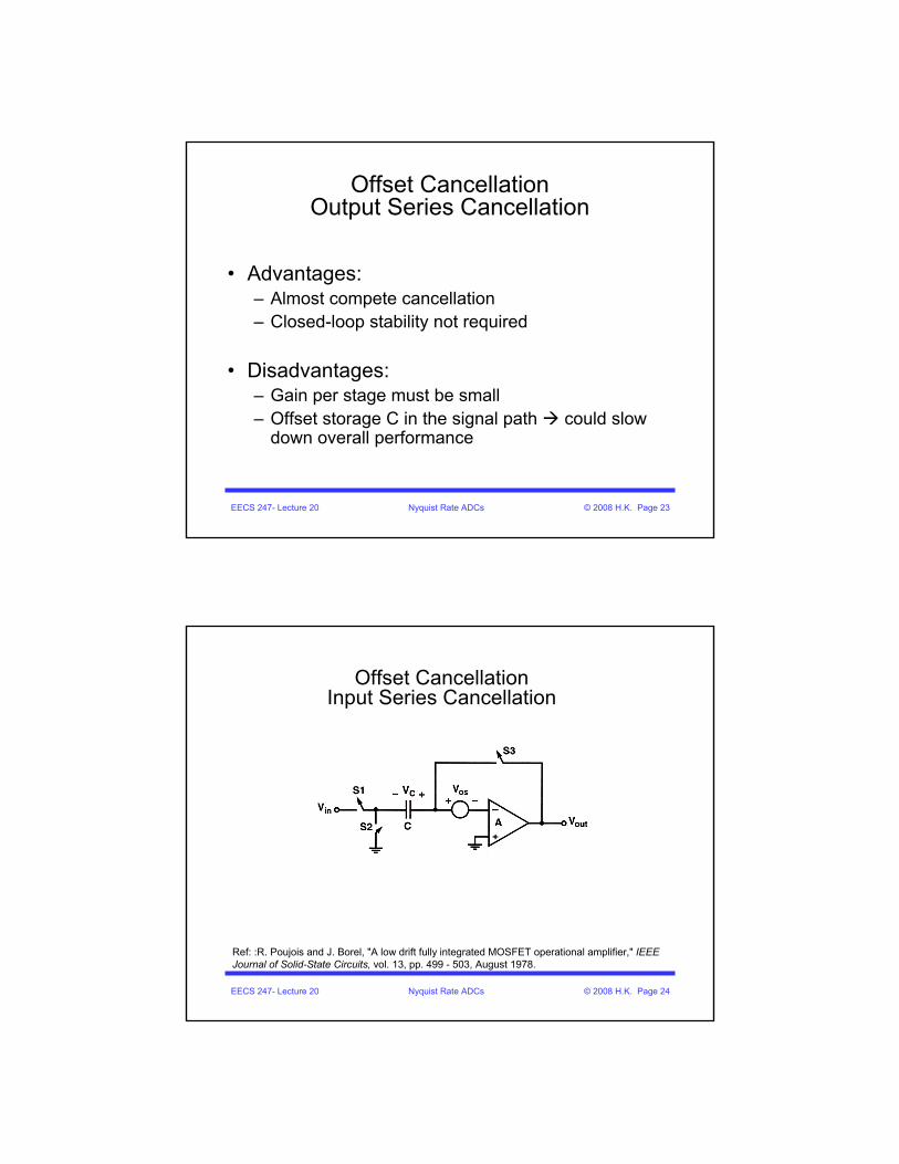
Offset CancellationOutput Series Cancellation
• Advantages:– Almost compete cancellation – Closed-loop stability not required
• Disadvantages:– Gain per stage must be small – Offset storage C in the signal path could slow
down overall performance
EECS 247- Lecture 20 Nyquist Rate ADCs © 2008 H.K. Page 24
Offset CancellationInput Series Cancellation
Ref: :R. Poujois and J. Borel, "A low drift fully integrated MOSFET operational amplifier," IEEE Journal of Solid-State Circuits, vol. 13, pp. 499 - 503, August 1978.
EECS 247- Lecture 20 Nyquist Rate ADCs © 2008 H.K. Page 25
Offset CancellationInput Series Cancellation
Ref: :R. Poujois and J. Borel, "A low drift fully integrated MOSFET operational amplifier," IEEE Journal of Solid-State Circuits, vol. 13, pp. 499 - 503, August 1978.
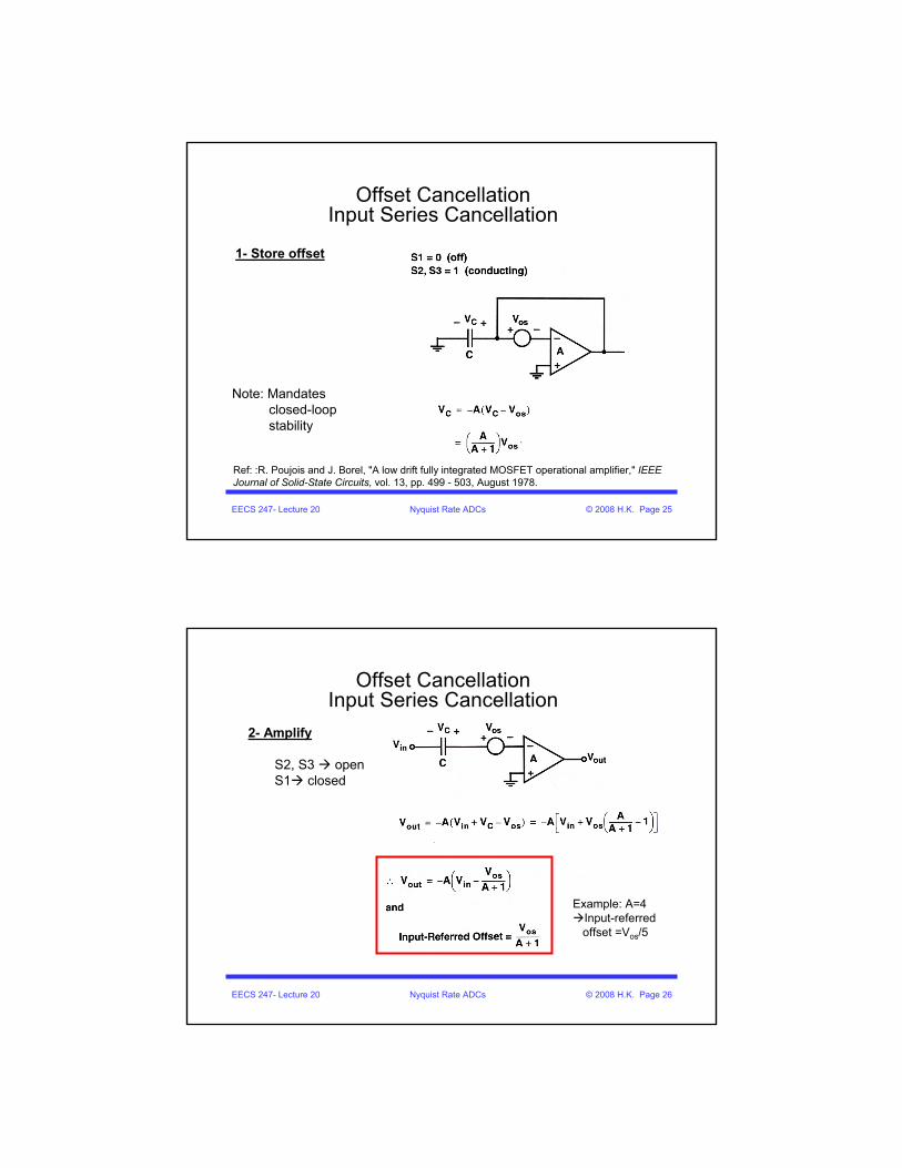
1- Store offset
Note: Mandates closed-loop stability
EECS 247- Lecture 20 Nyquist Rate ADCs © 2008 H.K. Page 26
Offset CancellationInput Series Cancellation
2- Amplify
S2, S3 openS1 closed
Example: A=4 Input-referred offset =Vos/5
EECS 247- Lecture 20 Nyquist Rate ADCs © 2008 H.K. Page 27
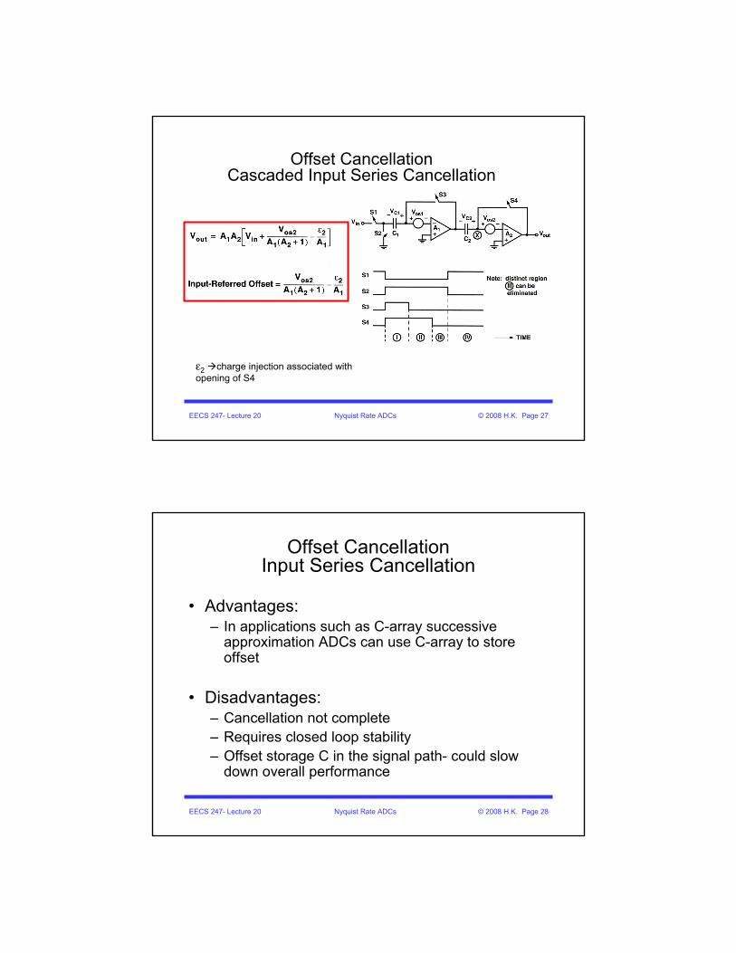
Offset CancellationCascaded Input Series Cancellation
ε2 charge injection associated with opening of S4
EECS 247- Lecture 20 Nyquist Rate ADCs © 2008 H.K. Page 28
Offset CancellationInput Series Cancellation
• Advantages:– In applications such as C-array successive
approximation ADCs can use C-array to store offset
• Disadvantages:– Cancellation not complete– Requires closed loop stability– Offset storage C in the signal path- could slow
down overall performance

EECS 247- Lecture 20 Nyquist Rate ADCs © 2008 H.K. Page 29
CMOS ComparatorsCascade of Gain Stages
Fully differential gain stages 1st order cancellation of switch feedthrough offset
1- Output series offset cancellation
2- Input series offset cancellation
EECS 247- Lecture 20 Nyquist Rate ADCs © 2008 H.K. Page 30
CMOS ComparatorsCascade of Gain Stages
3-Combined input & output series offset cancellation
EECS 247- Lecture 20 Nyquist Rate ADCs © 2008 H.K. Page 31
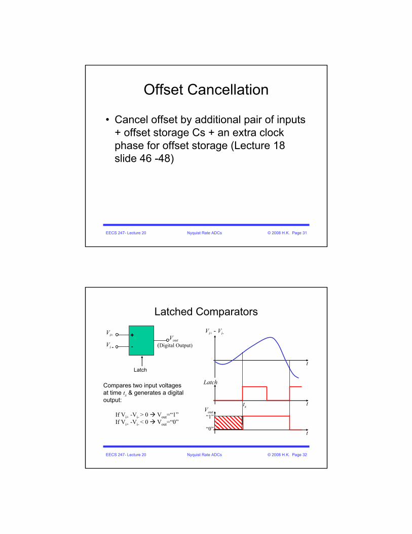
Offset Cancellation
• Cancel offset by additional pair of inputs + offset storage Cs + an extra clock phase for offset storage (Lecture 18 slide 46 -48)
EECS 247- Lecture 20 Nyquist Rate ADCs © 2008 H.K. Page 32
Latched Comparators
Vi+
Vi -Vout
(Digital Output)
+
-
Latch
Vout
Vi+ - Vi-
t
Latch
t
t
“1”
“0”
Compares two input voltages at time tx & generates a digital output:
If Vi+ -Vi- > 0 Vout=“1”If Vi+ -Vi- < 0 Vout=“0”
tx

EECS 247- Lecture 20 Nyquist Rate ADCs © 2008 H.K. Page 33
CMOS Latched Comparators
Comparator amplification need not be linearcan use a latch regeneration
Latch Amplification + positive feedback
EECS 247- Lecture 20 Nyquist Rate ADCs © 2008 H.K. Page 34
Simplest Form of CMOS Latch
VDD
M1 M2
M3
VDD
M1 M2
M4
EECS 247- Lecture 20 Nyquist Rate ADCs © 2008 H.K. Page 35
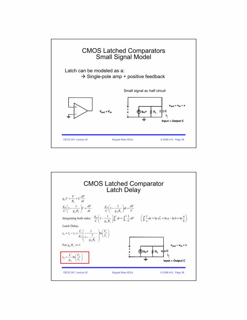
CMOS Latched ComparatorsSmall Signal Model
Latch can be modeled as a:Single-pole amp + positive feedback
Small signal ac half circuit
EECS 247- Lecture 20 Nyquist Rate ADCs © 2008 H.K. Page 36
CMOS Latched ComparatorLatch Delay
2 2
1 1
2D 2 1
1
1 11 1
1 1 1Integrating both sides: 1 ln ln ln ln
Latch Delay:1 ln11
mL
m m
m L m L
t V a amb
t V bm L
m
m L
V dVg V CR dt
g dV g dVV dtC g R dt C g R V
g adt dV dx x a bC g R V x b
C Vt t tg V
g R
= +
⎛ ⎞ ⎛ ⎞− = − =⎜ ⎟ ⎜ ⎟⎝ ⎠ ⎝ ⎠
⎛ ⎞ ⎛ ⎞− = = = − =⎜ ⎟⎜ ⎟ ⎝ ⎠⎝ ⎠
⎛ ⎞ ⎛ ⎞= − = ⎜ ⎟ ⎜⎝−⎜ ⎟⎜ ⎟
⎝ ⎠
∫ ∫ ∫
2D
1
For 1
ln
m L
m
g R
C Vtg V
⎟⎠
>>
⎛ ⎞≈ ⎜ ⎟⎝ ⎠

EECS 247- Lecture 20 Nyquist Rate ADCs © 2008 H.K. Page 37
CMOS Latched Comparators
2D
1
2
1
D
ln
ln
m
L
Lm
C Vtg V
V Latch Gain AV
Ct Ag
⎛ ⎞≈ ⎜ ⎟⎝ ⎠
→ =
→ ≈Compared to a 3-stage open-loop cascade of amps for equal overall gain of 1000
Latch faster by about x3
Normalized Latch Delay
D
m
tC
g
τD(3-stage amp)= 18.2(C/gm)
EECS 247- Lecture 20 Nyquist Rate ADCs © 2008 H.K. Page 38
Latch-Only Comparator
• Much faster compared to cascade of open-loop amplifiers
• Main problem associated with latch-only comparator topology:
– High input-referred offset voltage (as high as 100mV!)• Solution:
– Use preamplifier to amplify the signal and reduce overall input-referred offset

EECS 247- Lecture 20 Nyquist Rate ADCs © 2008 H.K. Page 39
Pre-Amplifier + LatchOverall Input-Referred Offset
LatchVi+
Vi-
Do+
Do-
fs
Preamp
Av
VosLatchVosPreamp
2 2Re _ _ Pr _2
Pr
_ Pr _ Pr
2 2Re _ 2
1
: 4 & 50 & 10
14 50 6.410
Input ferred Offset Vos eamp Vos Latcheamp
Vos eamp Vos Latch eamp
Input ferred Offset
A
Example mV mV A
mV
σ σ σ
σ σ
σ
−
−
= +
= = =
= + =
Latch offset attenuated by preamp gain when referred to preamp input.Assuming the two offset sources are uncorrelated:
EECS 247- Lecture 20 Nyquist Rate ADCs © 2008 H.K. Page 40
Pre-Amplifier Tradeoffs
• Example:– Latch offset 50 to 100mV– Preamp DC gain 10X– Preamp input-referred latch offset 50 to 100mV– Input-referred preamplifier offset 2 to 10mV– Overall input-referred offset 5.5 to 14mV
Addition of preamp reduces the latch input-referred offset reduced by ~7 to 9X ~allows extra 3-bit resolution for ADC!
LatchVi+
Vi-
Do+
Do-
fs
Preamp
Av
EECS 247- Lecture 20 Nyquist Rate ADCs © 2008 H.K. Page 41
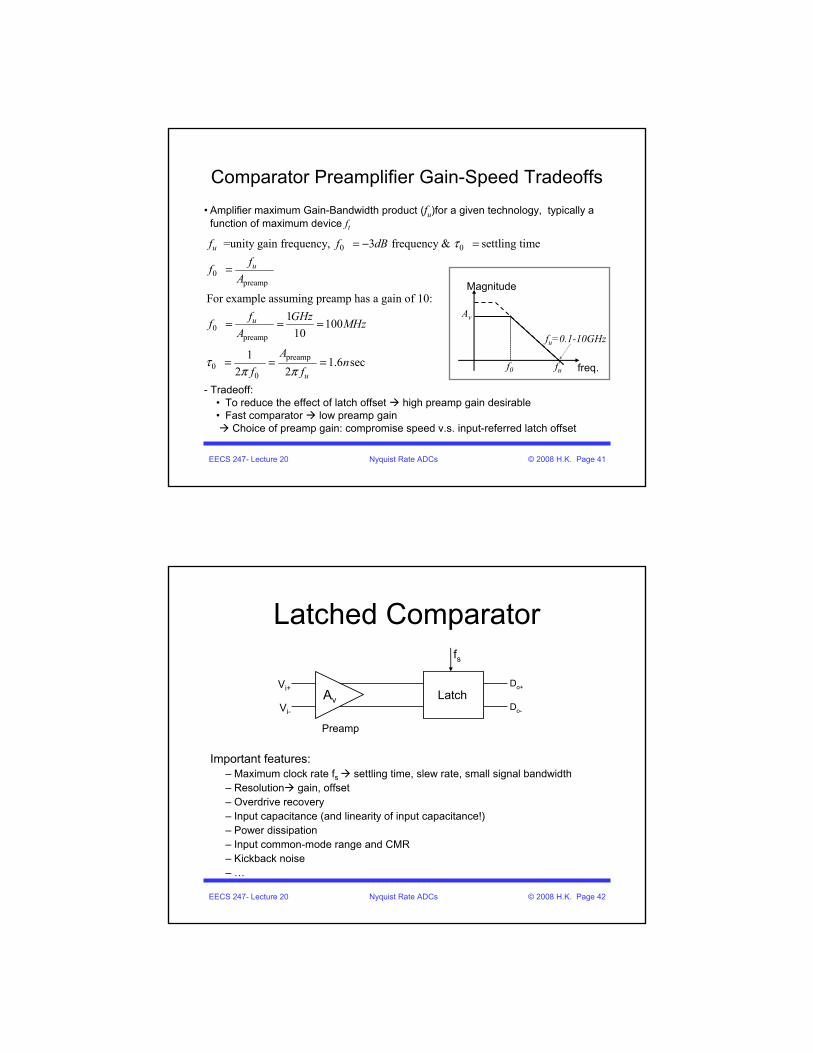
Comparator Preamplifier Gain-Speed Tradeoffs• Amplifier maximum Gain-Bandwidth product (fu)for a given technology, typically a
function of maximum device ft
- Tradeoff:• To reduce the effect of latch offset high preamp gain desirable• Fast comparator low preamp gain
Choice of preamp gain: compromise speed v.s. input-referred latch offset
fu=0.1-10GHz
f0 fu freq.
Magnitude
Av
0 0
0
preamp
0
preamp
preamp 0
0
=unity gain frequency, 3 frequency & settling time
For example assuming preamp has a gain of 10:1 100
10
1 1.6 sec2 2
u
u
u
u
f f dBff
A
f GHzf MHzA
An
f f
τ
τπ π
= − =
=
= = =
= = =
EECS 247- Lecture 20 Nyquist Rate ADCs © 2008 H.K. Page 42
Latched Comparator
Av LatchVi+
Vi-
Do+
Do-
fs
Preamp
Important features:– Maximum clock rate fs settling time, slew rate, small signal bandwidth– Resolution gain, offset– Overdrive recovery– Input capacitance (and linearity of input capacitance!)– Power dissipation– Input common-mode range and CMR – Kickback noise– …
EECS 247- Lecture 20 Nyquist Rate ADCs © 2008 H.K. Page 43
Comparator Overdrive Recovery
U amplification after time ta
During reset amplifier settles exponentially to its zero input condition with τ0=RC
Assume Vm maximum input normalized to 1/2lsb (=1)
Linear model for a single-pole amplifier:
Example: Worst case input/output waveforms
Previous input max. possible e.g. VFSCurrent input min. input-referred signal
(0.5LSB)
EECS 247- Lecture 20 Nyquist Rate ADCs © 2008 H.K. Page 44
Comparators Overdrive Recovery
Example: Worst case input/output waveforms
If recovery time is not long enough to allow output to discharge (recover) from previous state- then it may not be able to resolve the current input errorTo minimize this effect:
1. Passive clamp2. Active restore3. Low gain/stage

EECS 247- Lecture 20 Nyquist Rate ADCs © 2008 H.K. Page 45
Comparators Overdrive RecoveryLimiting Output Voltage
ClampAdds parasitic capacitance
Active RestoreAfter outputs are latched by following stage
Activate φR & equalize output nodes
EECS 247- Lecture 20 Nyquist Rate ADCs © 2008 H.K. Page 46
CMOS Preamplifier + Latched Comparator Delay in Response
2D
1
1
0D
Latch delay previously found:
ln
Assuming gain of for the preamplifier then :
ln
m
v v in
m v in
VCg V
A V A V
VCg A V
τ
τ
⎛ ⎞⎜ ⎟⎝ ⎠
= ×
⎛ ⎞⎜ ⎟⎝ ⎠
≈
≈
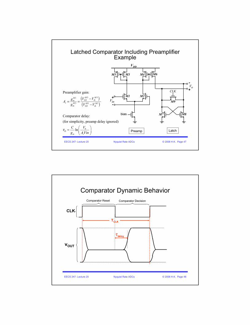
EECS 247- Lecture 20 Nyquist Rate ADCs © 2008 H.K. Page 47
Latched Comparator Including PreamplifierExample
oV
inV
-+
+
-
M1 M2CLK
M3 M4
VDD
M7 M8bias
M5 M6
M9
Preamp Latch
( )( )
3 31
3 1 1
0D
Preamplifier gain:
Comparator delay: (for simplicity, preamp delay ignored)
ln
M MMGS thm
v M M Mm GS th
m v
V VgAg V V
C Vg A Vin
τ
−= =
−
⎛ ⎞≈ ⎜ ⎟⎝ ⎠
EECS 247- Lecture 20 Nyquist Rate ADCs © 2008 H.K. Page 48
Comparator Dynamic Behavior
vOUT
CLK
TCLK
τdelay
Comparator Reset Comparator Decision

EECS 247- Lecture 20 Nyquist Rate ADCs © 2008 H.K. Page 49
Comparator Resolution
VIN =10mV 1mV
0.1mV10μVvOUT
CLK
Δt = (gm/C).ln(Vin1/Vin2)
EECS 247- Lecture 20 Nyquist Rate ADCs © 2008 H.K. Page 50
Comparator Voltage Transfer FunctionNon-Idealities
Vout
Vin
VOffset
ε
-0.5LSB 0.5LSB
VOffset Comparator offset voltage
ε Meta-Stable region (output ambiguous)
EECS 247- Lecture 20 Nyquist Rate ADCs © 2008 H.K. Page 51
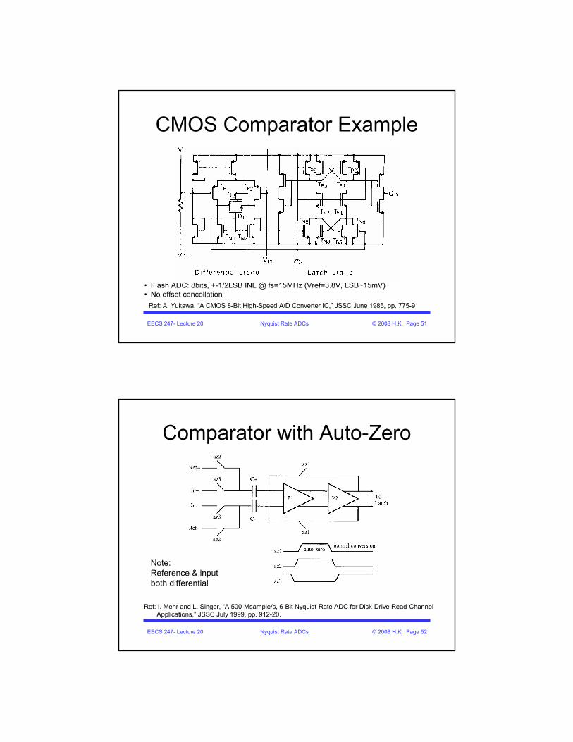
CMOS Comparator Example
Ref: A. Yukawa, “A CMOS 8-Bit High-Speed A/D Converter IC,” JSSC June 1985, pp. 775-9
• Flash ADC: 8bits, +-1/2LSB INL @ fs=15MHz (Vref=3.8V, LSB~15mV)• No offset cancellation
EECS 247- Lecture 20 Nyquist Rate ADCs © 2008 H.K. Page 52
Comparator with Auto-Zero
Ref: I. Mehr and L. Singer, “A 500-Msample/s, 6-Bit Nyquist-Rate ADC for Disk-Drive Read-Channel Applications,” JSSC July 1999, pp. 912-20.
Note: Reference & input both differential

EECS 247- Lecture 20 Nyquist Rate ADCs © 2008 H.K. Page 53
Ref: I. Mehr and D. Dalton, “A 500-Msample/s, 6-Bit Nyquist-Rate ADC for Disk-Drive Read-Channel Applications,” JSSC July 1999, pp. 912-20.
Voffset
( )C C
Re f Re f Offset
V VV V V
+ −
+ −
− =− −
Flash ADCComparator with Auto-Zero
EECS 247- Lecture 20 Nyquist Rate ADCs © 2008 H.K. Page 54
Ref: I. Mehr and D. Dalton, “A 500-Msample/s, 6-Bit Nyquist-Rate ADC for Disk-Drive Read-Channel Applications,” JSSC July 1999, pp. 912-20.
Voffset
Vo
( ) ( )[ ]( )
( ) ( )
Offseto P1 P2 In In C C
C C
Re f Re fo P1 P2 In In
VV A A V V V V
Subst i tut ing for from previous cycle:V V
V VV A A V V
Note: Of fset i s cancel led & di f ference betweeninput & reference es tabl ished
+ − + −
+ −
+ −+ −
− −= ∗ − −
−
−= ∗ −⎡ ⎤−⎣ ⎦
Flash ADCComparator with Auto-Zero

EECS 247- Lecture 20 Nyquist Rate ADCs © 2008 H.K. Page 55
Ref: I. Mehr and D. Dalton, “A 500-Msample/s, 6-Bit Nyquist-Rate ADC for Disk-Drive Read-Channel Applications,” JSSC July 1999, pp. 912-20.
Flash ADCUsing Comparator with Auto-Zero
EECS 247- Lecture 20 Nyquist Rate ADCs © 2008 H.K. Page 56
Auto-Zero Implementation
Ref:I. Mehr and L. Singer, “A 55-mW, 10-bit, 40-Msample/s Nyquist-Rate CMOS ADC,” JSSC March 2000, pp. 318-25
EECS 247- Lecture 20 Nyquist Rate ADCs © 2008 H.K. Page 57
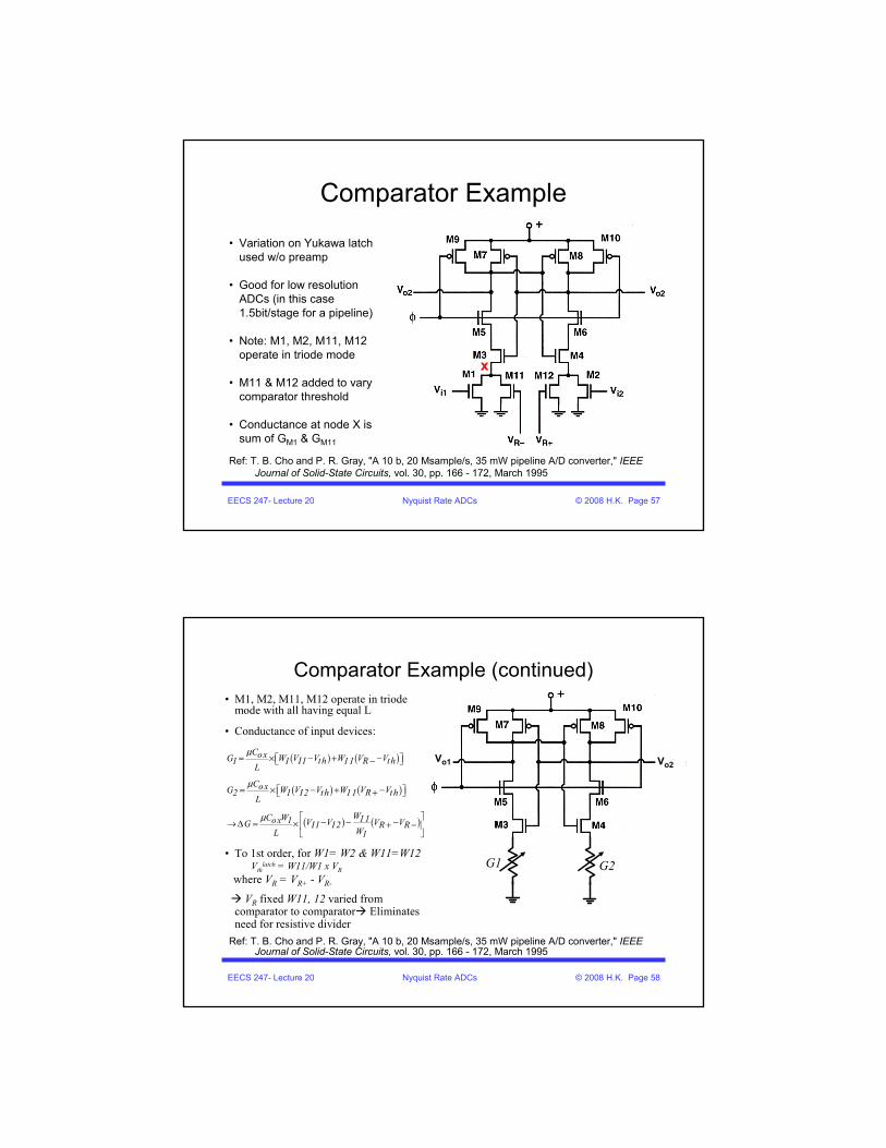
Comparator Example
Ref: T. B. Cho and P. R. Gray, "A 10 b, 20 Msample/s, 35 mW pipeline A/D converter," IEEE Journal of Solid-State Circuits, vol. 30, pp. 166 - 172, March 1995
• Variation on Yukawa latch used w/o preamp
• Good for low resolution ADCs (in this case 1.5bit/stage for a pipeline)
• Note: M1, M2, M11, M12 operate in triode mode
• M11 & M12 added to vary comparator threshold
• Conductance at node X is sum of GM1 & GM11
x
EECS 247- Lecture 20 Nyquist Rate ADCs © 2008 H.K. Page 58
Comparator Example (continued)
Ref: T. B. Cho and P. R. Gray, "A 10 b, 20 Msample/s, 35 mW pipeline A/D converter," IEEE Journal of Solid-State Circuits, vol. 30, pp. 166 - 172, March 1995
Vo1
G1 G2
( ) ( )
( ) ( )
( ) ( )
Cox V V V VG W WI1 th R th1 1 11L
Cox V V V VG W WI2 th R th2 1 11L
WC W 11ox 1 V V V VG I1 I2 R RWL 1
μ
μ
μ
− −= × +⎡ ⎤−⎣ ⎦
− −= × +⎡ ⎤+⎣ ⎦
⎡ ⎤− −−→ Δ = × + −⎢ ⎥⎣ ⎦
Vo1 Vo2
• M1, M2, M11, M12 operate in triode mode with all having equal L
• Conductance of input devices:
• To 1st order, for W1= W2 & W11=W12Vth
latch = W11/W1 x VR
where VR = VR+ - VR-
VR fixed W11, 12 varied from comparator to comparator Eliminates need for resistive divider
EECS 247- Lecture 20 Nyquist Rate ADCs © 2008 H.K. Page 59
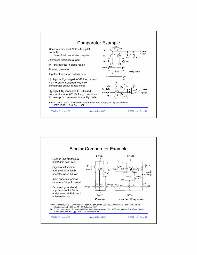
Comparator Example• Used in a pipelined ADC with digital
correctionno offset cancellation required
Differential reference & input
• M7, M8 operate in triode region
• Preamp gain ~10
• Input buffers suppress kick-back
• φ1 high Cs charged to VR & φ2B is also high current diverted to latchcomparator output in hold mode
• φ2 high Cs connected to S/Hout & comparator input (VR-S/Hout), current sent to preamp comparator in amplify mode
Ref: S. Lewis, et al., “A Pipelined 5-Msample/s 9-bit Analog-to-Digital Converter”IEEE JSSC ,NO. 6, Dec. 1987
EECS 247- Lecture 20 Nyquist Rate ADCs © 2008 H.K. Page 60
Bipolar Comparator Example
• Used in 8bit 400Ms/s & 6bit 2Gb/s flash ADC
• Signal amplification during φ1 high, latch operates when φ1 low
• Input buffers suppress kick-back & input current
• Separate ground and supply buses for front-end preamp kick-back noise reduction
Ref: Y. Akazawa, et al., "A 400MSPS 8b flash AD conversion LSI," IEEE International Solid-State Circuits Conference, vol. XXX, pp. 98 - 99, February 1987
Ref: T. Wakimoto, et al, "Si bipolar 2GS/s 6b flash A/D conversion LSI," IEEE International Solid-State Circuits Conference, vol. XXXI, pp. 232 - 233, February 1988
Preamp Latched Comparator