EE2301 POWER ELECTRONICS Unit-1 - Fmcetfmcet.in/EEE/EE2301_uw.pdfEE2301 POWER ELECTRONICS Unit-1....
175
EE2301 POWER ELECTRONICS Unit-1
Transcript of EE2301 POWER ELECTRONICS Unit-1 - Fmcetfmcet.in/EEE/EE2301_uw.pdfEE2301 POWER ELECTRONICS Unit-1....

EE2301 POWER ELECTRONICS
Unit-1

Introduction
• What are Power Semiconductor Devices (PSD)?
They are devices used as switches or rectifiers in
power electronic circuits
• What is the difference of PSD and low-power
semiconductor device?
Large voltage in the off state
High current capability in the on state

Classification
Fig. 1. The power semiconductor devices family

Important Parameters
• Breakdown voltage.
• On-resistance.
Trade-off between breakdown voltage and on-resistance.
• Rise and fall times for switching between on
and off states.
• Safe-operating area.

Power MOSFET: Structure
Power MOSFET has much higher current handling capability in
ampere range and drain to source blocking voltage(50-100V)
than other MOSFETs.
Fig.2.Repetitive pattern of the cells structure in power MOSFET
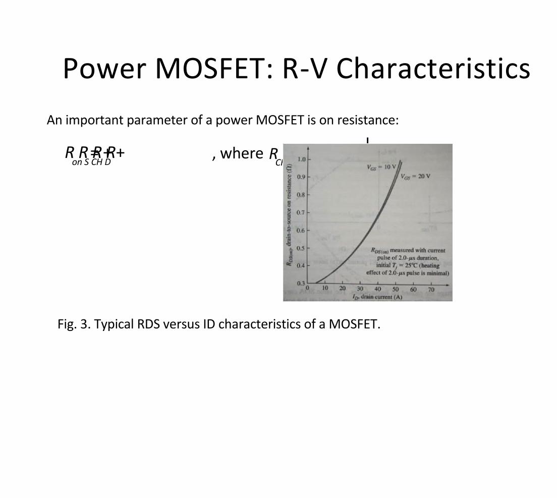
Power MOSFET: R-V Characteristics
An important parameter of a power MOSFET is on resistance:
L R R R R = + + , where R W C V V =
µ on S CH D ( ) - CH
n ox GS T
Fig. 3. Typical RDS versus ID characteristics of a MOSFET.

Thyristor: Structure • Thyristor is a general class of a four-layer pnpn
semiconducting device.
Fig.4 (a) The basic four-layer pnpn structure.
(b) Two two-transistor equivalent circuit.

Thyristor: I-V Characteristics
Three States:
Reverse Blocking
Forward Blocking
Forward Conducting
Fig.5 The current-voltage
characteristics of the pnpn device.
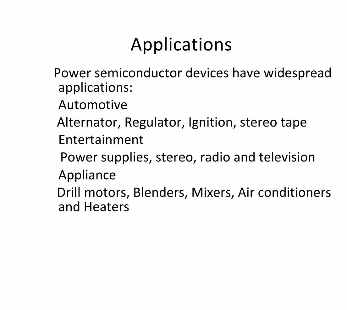
Applications
Power semiconductor devices have widespread applications:
Automotive
Alternator, Regulator, Ignition, stereo tape
Entertainment
Power supplies, stereo, radio and television
Appliance
Drill motors, Blenders, Mixers, Air conditioners and Heaters

Thyristors
• Most important type of power semiconductor device.
• Have the highest power handling capability.they have a rating of 1200V / 1500A with switching frequencies ranging from 1KHz to 20KHz.
• Is inherently a slow switching device compared to BJT or MOSFET.
• Used as a latching switch that can be turned on by the control terminal but cannot be turned off by the gate.

Different types of Thyristors
• Silicon Controlled Rectifier (SCR).
• TRIAC.
• DIAC.
• Gate Turn-Off Thyristor (GTO).

SCR
Symbol of
Silicon Controlled Rectifier

Structure
Cathode Gate
} 19 -3 19 -3 10 cm 10 cm 10 m µ n+ n+
} J3
} 17 -3
10 cm 30-100 m µ p-
J2
50-1000 m µ 13 14 -3 10 -5 x 10 cm n–
} J1 30-50 m µ 17 -3 p 10 cm
19 -3 10 cm p+
Anode

Device Operation
Simplified model of a
thyristor

V-I Characteristics

Effects of gate current
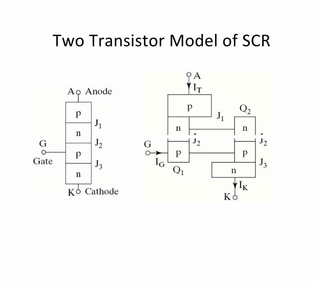
Two Transistor Model of SCR


Considering PNP transistor
of the equivalent circuit,
a a , , , I I I I = = = 1 E A C C 1 1
, I I I I = = CBO CBO B B
1 1
( ) ( ) a 1 1 I I I = - - - - - 1 B A CBO 1 1

Considering NPN transistor
of the equivalent circuit,
, , I I I I I I I I = = = = + C C B B E K A G
2 2 2
a I I I = + 2 C k CBO
2 2
( ) ( ) a 2 I I I I = + + - - - 2 C A G CBO 2 2

From the equivalent circuit,
we see that
I I = C B
2 1
I I I + + I a = 2 1 2 g CBO CBO
( ) a a 1 - + A
1 2

Case 1: When 0 I = g
I I + I = - + CBO CBO
( ) 1 2
a a 1 A
1 2
Case 2: When 0 I G
I I I + + I a = 2 1 2 g CBO CBO
( ) a a 1 - + A
1 2

Turn-on Characteristics
t t t = + o n d r
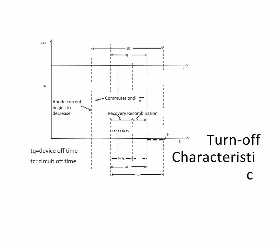
VAK
tC
tq
t
IA
Commutationdi dt Anode current
begins to
decrease Recovery Recombination
t1 t2 t3 t4 t5
Turn-off t
tq=device off time
Characteristi trr tgr
tc=circuit off time tq
c tc

Methods of Thyristor Turn-on
• Thermal Turn-on.
• Light.
• High Voltage.
• Gate Current.
• dv/dt.
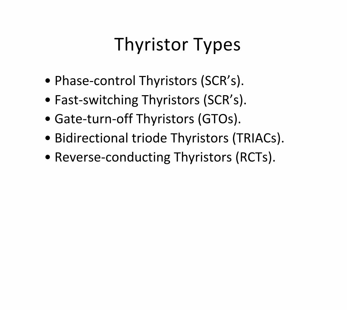
Thyristor Types
• Phase-control Thyristors SCR’s . • Fast-switching Thyristors SCR’s . • Gate-turn-off Thyristors (GTOs).
• Bidirectional triode Thyristors (TRIACs).
• Reverse-conducting Thyristors (RCTs).
• Static induction Thyristors (SITHs).
• Light-activated silicon-controlled rectifiers (LASCRs).
• FET controlled Thyristors (FET-CTHs).
• MOS controlled Thyristors (MCTs).
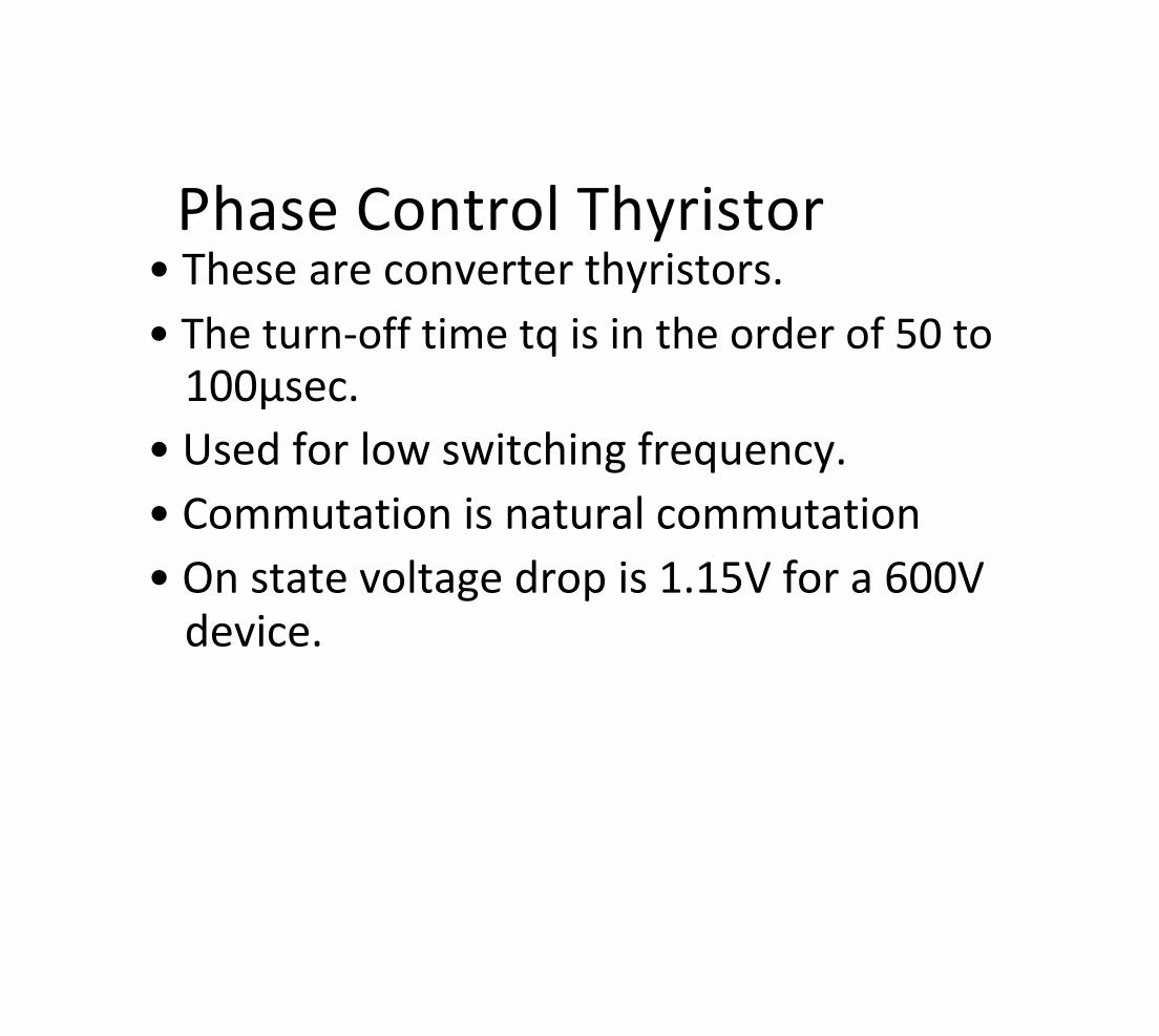
Phase Control Thyristor • These are converter thyristors.
• The turn-off time tq is in the order of 50 to
100µsec.
• Used for low switching frequency.
• Commutation is natural commutation
• On state voltage drop is 1.15V for a 600V device.

• They use amplifying gate thyristor.

Fast Switching Thyristors
• Also called inverter thyristors.
• Used for high speed switching applications.
• Turn-off time tq in the range of 5 to 50µsec.
• On-state voltage drop of typically 1.7V for
2200A, 1800V thyristor.
• High dv/dt and high di/dt rating.
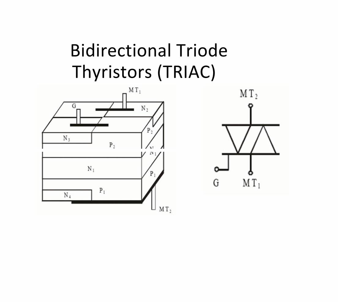
Bidirectional Triode Thyristors (TRIAC)
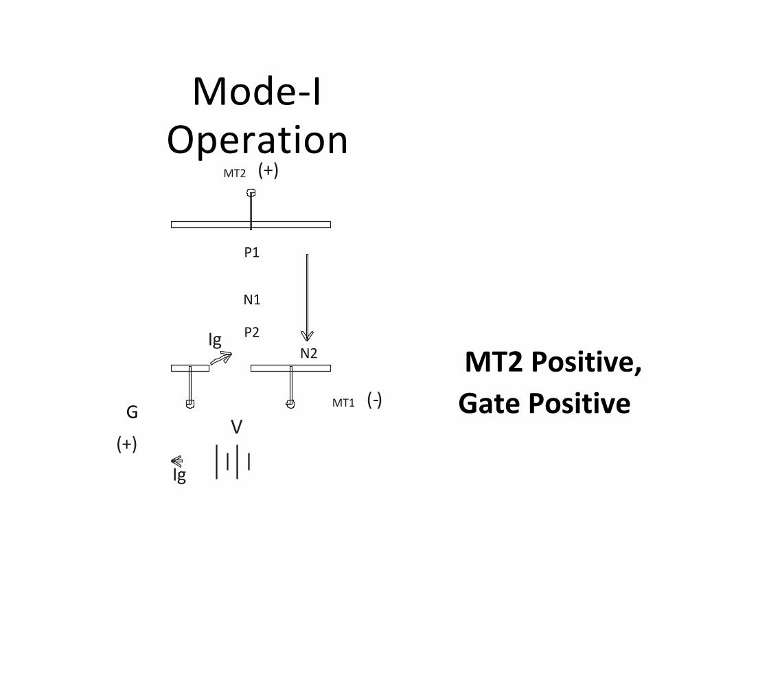
Mode-I Operation
(+) MT2
P1
N1
P2 Ig
MT2 Positive, N2
Gate Positive ( ) - MT1 G
V (+)
Ig

Mode-II Operation
(+) MT2
P1
Final Initial N1 conduction conduction
P2
MT2 Positive, N2 N3
Gate Negative ( ) - MT1 G
V
Ig
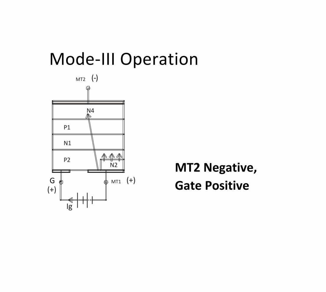
Mode-III Operation ( ) - MT2
N4
P1
N1
P2
MT2 Negative, N2
(+) G Gate Positive
MT1
(+)
Ig

Mode-IV Operation ( ) - MT2
N4
P1
N1
MT2 Negative, P2
N3
Gate Negative (+) G MT1
(-)
Ig
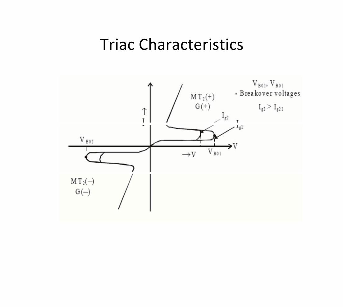
Triac Characteristics

BJT structure heavily doped ~ 10^15 provides the carriers lightly doped ~ 10^8 lightly doped ~ 10^6
note: this is a current of electrons (npn case) and so the conventional current flows from collector to emitter.

BJT characteristics

BJT characteristics
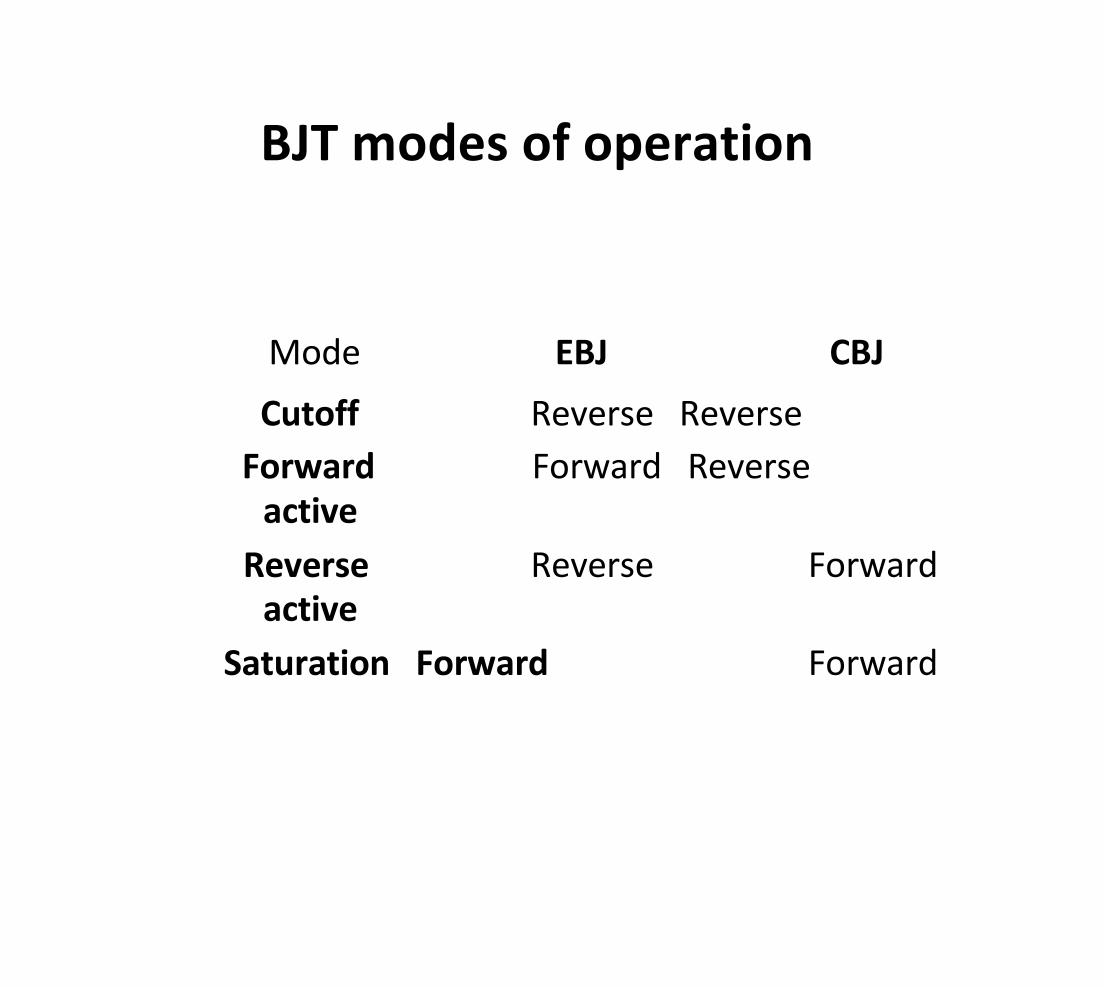
BJT modes of operation
Mode EBJ CBJ
Cutoff Reverse Reverse
Forward Forward Reverse
active
Reverse Reverse Forward
active
Saturation Forward Forward
BJT modes of operation
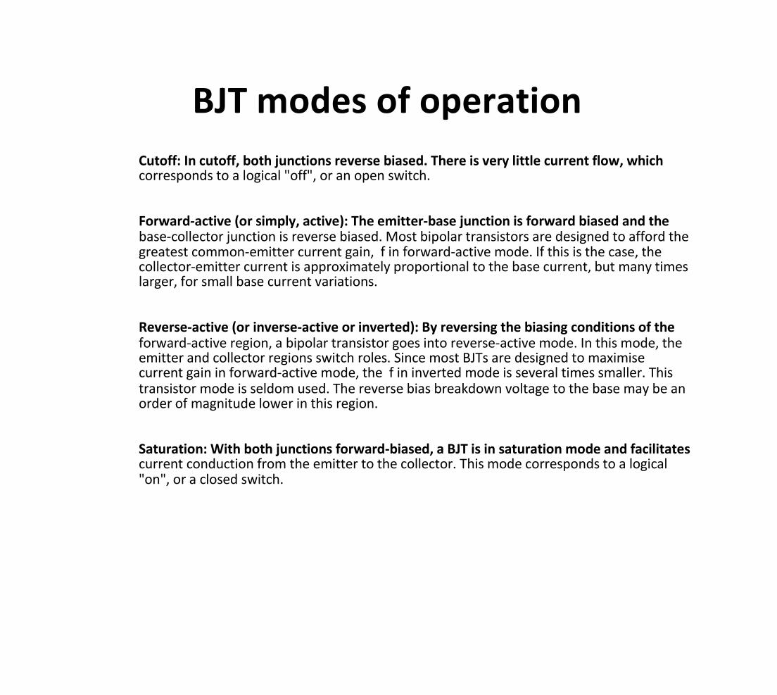
Cutoff: In cutoff, both junctions reverse biased. There is very little current flow, which corresponds to a logical "off", or an open switch. Forward-active (or simply, active): The emitter-base junction is forward biased and the base-collector junction is reverse biased. Most bipolar transistors are designed to afford the greatest common-emitter current gain, f in forward-active mode. If this is the case, the collector-emitter current is approximately proportional to the base current, but many times larger, for small base current variations. Reverse-active (or inverse-active or inverted): By reversing the biasing conditions of the forward-active region, a bipolar transistor goes into reverse-active mode. In this mode, the emitter and collector regions switch roles. Since most BJTs are designed to maximise current gain in forward-active mode, the f in inverted mode is several times smaller. This transistor mode is seldom used. The reverse bias breakdown voltage to the base may be an order of magnitude lower in this region. Saturation: With both junctions forward-biased, a BJT is in saturation mode and facilitates current conduction from the emitter to the collector. This mode corresponds to a logical "on", or a closed switch.


UNIT II
PHASE CONTROLLED
CONVERTERS

Phase-Control Converters
Single-Phase
Semiconverter
Three-Phase
Full converter
Dual converter
Semiconverter
Full converter
Dual converter
www.Vidyarthiplus.com
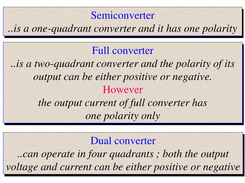
Semiconverter
..is a one-quadrant converter and it has one polarity
Full converter
..is a two-quadrant converter and the polarity of its
output can be either positive or negative.
However
the output current of full converter has
one polarity only
Dual converter ..can operate in four quadrants ; both the output
voltage and current can be either positive or negative
www.Vidyarthiplus.com

www.Vidyarthiplus.com
cos12
sin2
1 mmdc
VttdVV
Average Output Voltage
m
dm
VV Maximum
Output Voltage
cos15.0 dm
dcn
V
VVNormalizing
Output Voltage
2
2sin1
2sin
2
1 22
mmrms
VttdVV
RMS Output Voltage
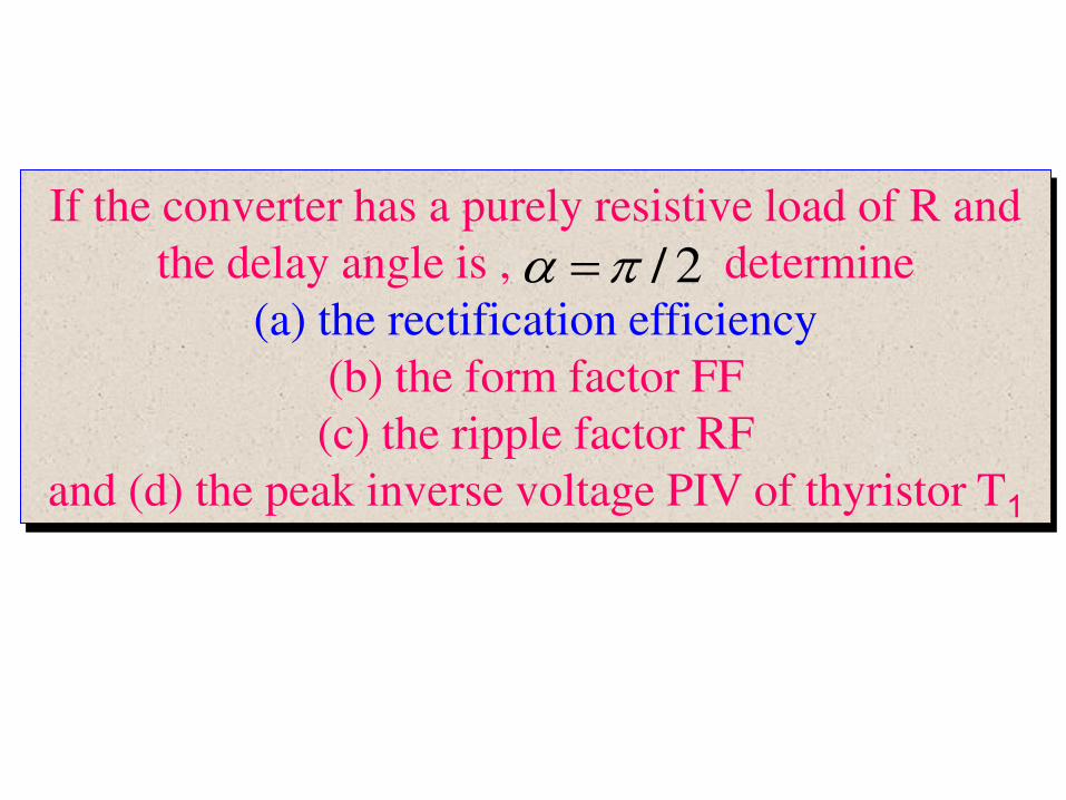
If the converter has a purely resistive load of R and
the delay angle is , determine (a) the rectification efficiency
(b) the form factor FF (c) the ripple factor RF
and (d) the peak inverse voltage PIV of thyristor T1
2/
www.Vidyarthiplus.com
%27.203536.0
1592.0
3536.02
22
sin2
1
2
1592.0
2cos1
2sin
2
1
2
2
2
2
2
m
m
rms
dc
mm
rms
mdc
mmdc
V
V
V
V
VV
V
VV
VttdVV

If the converter has a purely resistive load of R and
the delay angle is , determine (a) the rectification efficiency
(b) the form factor FF
(c) the ripple factor RF and (d) the peak inverse voltage PIV of thyristor T1
2/
221.21592.0
3536.0
m
m
dc
rms
V
V
V
VFF
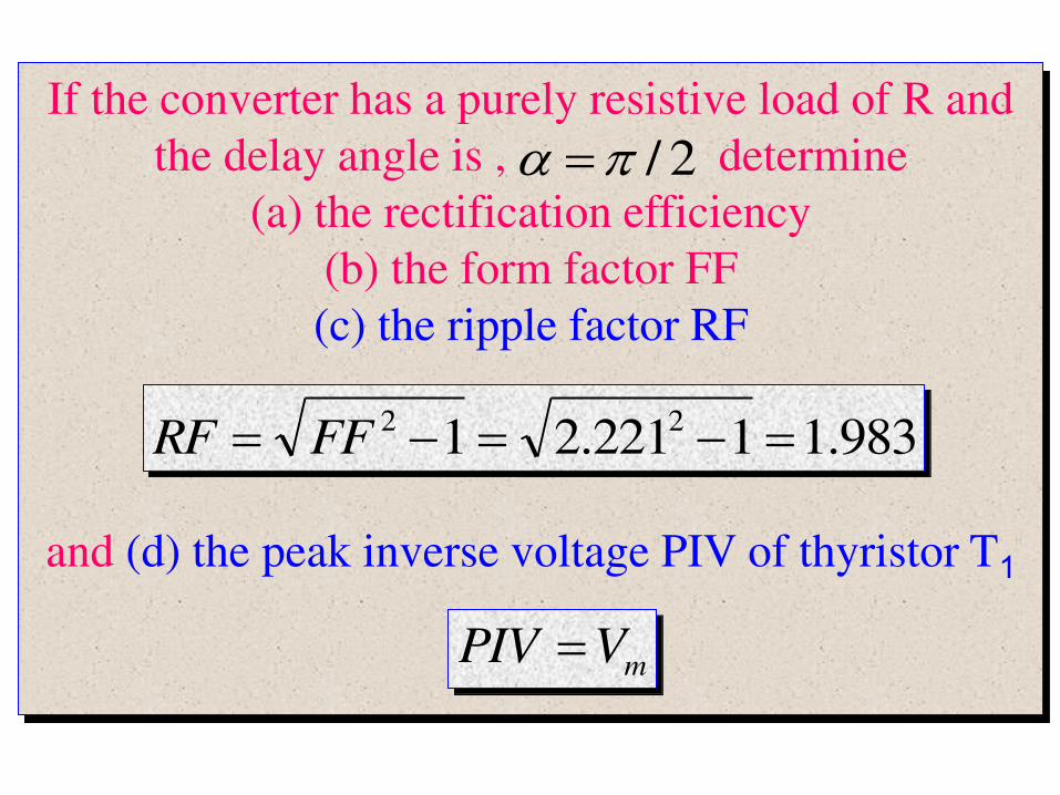
If the converter has a purely resistive load of R and
the delay angle is , determine (a) the rectification efficiency
(b) the form factor FF
(c) the ripple factor RF
and (d) the peak inverse voltage PIV of thyristor T1
2/
983.11221.21 22 FFRF
mVPIV
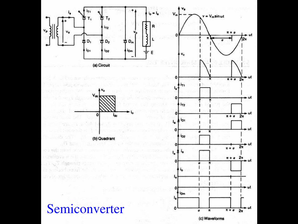
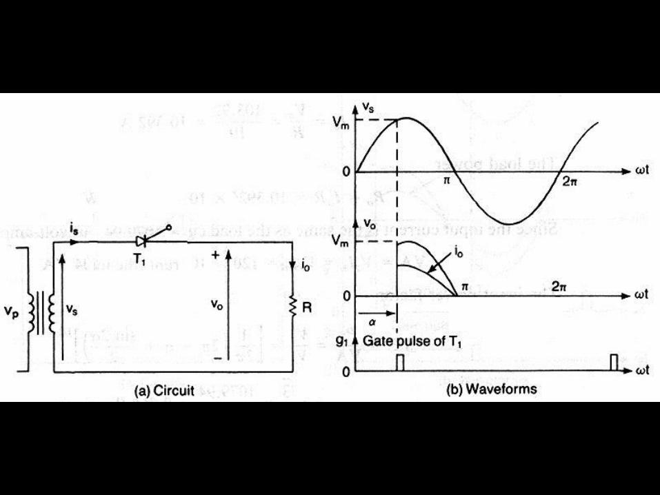
www.Vidyarthiplus.com Semiconverter
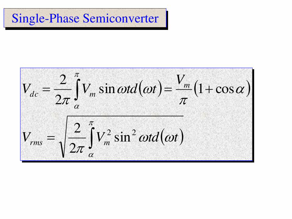
Single-Phase Semiconverter
ttdVV
VttdVV
mrms
mmdc
22 sin2
2
cos1sin2
2

www.Vidyarthiplus.com
Single-Phase Semiconverter (RL-load)
L
R
L
R
LLL
LL
eR
EeItiI
ERidt
diL
1
0
011
11
tL
R
SL
SL
SLL
eZ
V
R
EI
R
Et
Z
VI
tVERidt
diL
sin2
sin2
sin2
12
22
Mode 1
t0
Mode 2
tR
L 1tan 22LRZ

www.Vidyarthiplus.com
Single-Phase Semiconverter (RL-load)
RMS Current
for Thyristor
tdiI LR
2
22
1
RMS Current
for Thyristor
tdiI LA 2
2
1
RMS Output
Current
tditdiI LLrms
2
20
2
12
1
2
1
AVG Output
Current
tditdiIdc 2
01
2
1
2
1

The single-phase semiconverter has an RL load of
L = 6.5mH, R = 2.5 Ohm, and E = 10 V. The input
voltage is VS = 120 V(rms) at 60 Hz. Determine
(a) the load current IL0 at , and the load
current IL1 at , (b) the average thyristor current IA
(c) the rms thyristor current IR (d) the rms output current Irms
and (e) the average output current Idc
0t 60t

www.Vidyarthiplus.com
Single-Phase
Full Converter
Rectification
Mode
Inversion
Mode

Single-Phase Full Converter
2
sin2
2
cos2
sin2
2
22 mmrms
mmdc
VtdtVV
VtdtVV

Single-Phase Full Converter (RL-load)
tL
R
SL
SL e
Z
V
R
EI
R
Et
Z
VI
sin2
sin2
0
Mode 1 = Mode 2 R
L 1tan 22LRZ

www.Vidyarthiplus.com
Single-Phase Full Converter (RL-load)
RMS Current
for Thyristor
tdiI LR
2
2
1
RMS Current
for Thyristor
tdiI LA
2
1
RMS Output
Current RRRrms IIII 222
AVG Output
Current AAAdc IIII 2
www.Vidyarthiplus.com
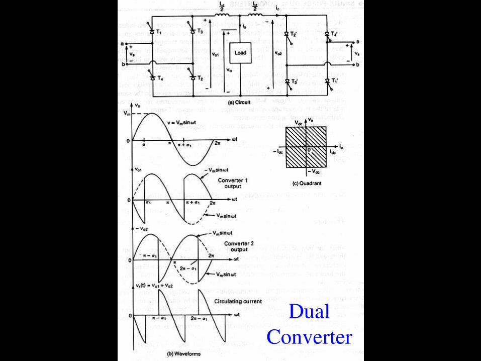
Dual Converter

www.Vidyarthiplus.com
Single-Phase Dual Converter
High-Power Variable-Speed Drives
21
22
11
cos2
cos2
dcdc
mdc
mdc
VV
VV
VV

www.Vidyarthiplus.com
Three-Phase Semiconverter
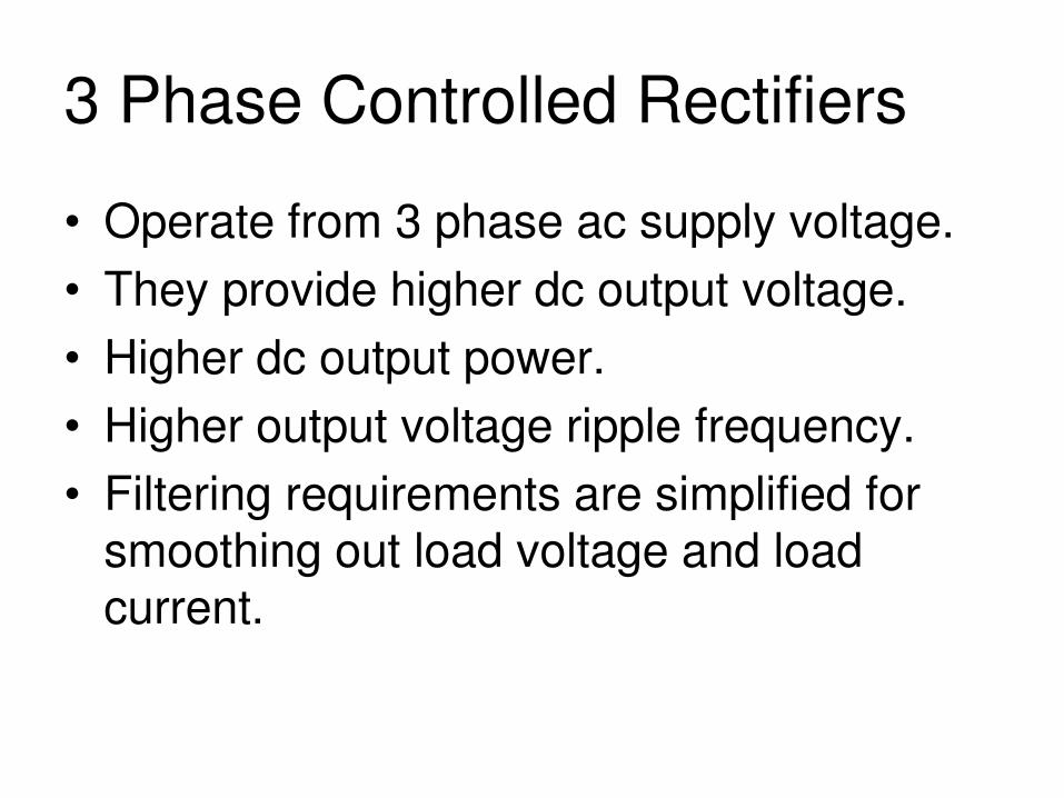
3 Phase Controlled Rectifiers
• Operate from 3 phase ac supply voltage.
• They provide higher dc output voltage.
• Higher dc output power.
• Higher output voltage ripple frequency.
• Filtering requirements are simplified for
smoothing out load voltage and load current.

• Extensively used in high power variable speed industrial dc drives.
• Three single phase half-wave converters
can be connected together to form a three phase half-wave converter.

3-Phase
Half Wave Converter (3-Pulse Converter)
with RL Load
Continuous & Constant Load Current Operation


Vector Diagram of 3 Phase Supply Voltages
VAN
VCN
VBN
1200
1200
1200 RN AN
YN BN
BN CN
v v
v v
v v
3 Phase Supply Voltage
Equations
We deifine three line to neutral voltages
(3 phase voltages) as follows

0
0
0
sin ;
Max. Phase Voltage
2sin
3
sin 120
2sin
3
sin 120
sin 240
RN an m
m
YN bn m
m
BN cn m
m
m
v v V t
V
v v V t
V t
v v V t
V t
V t

van vbn vcn van
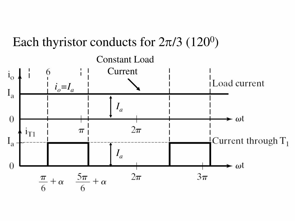
io=Ia
Constant Load
Current
Ia
Ia
Each thyristor conducts for 2/3 (1200)

To Derive an
Expression for the
Average Output Voltage of a
3-Phase Half Wave Converter
with RL Load
for Continuous Load Current
0
1
0
2
0
3
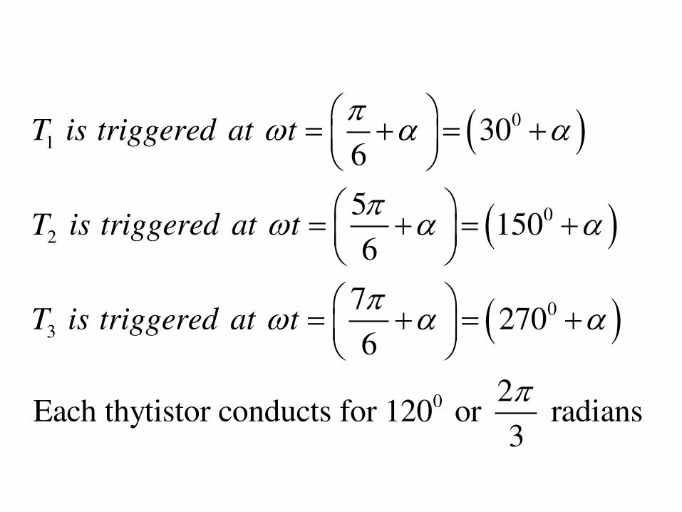
0
306
5 150
6
7 270
6
2Each thytistor conducts for 120 or radians
3
T is triggered at t
T is triggered at t
T is triggered at t
5
6
6
5
6
6
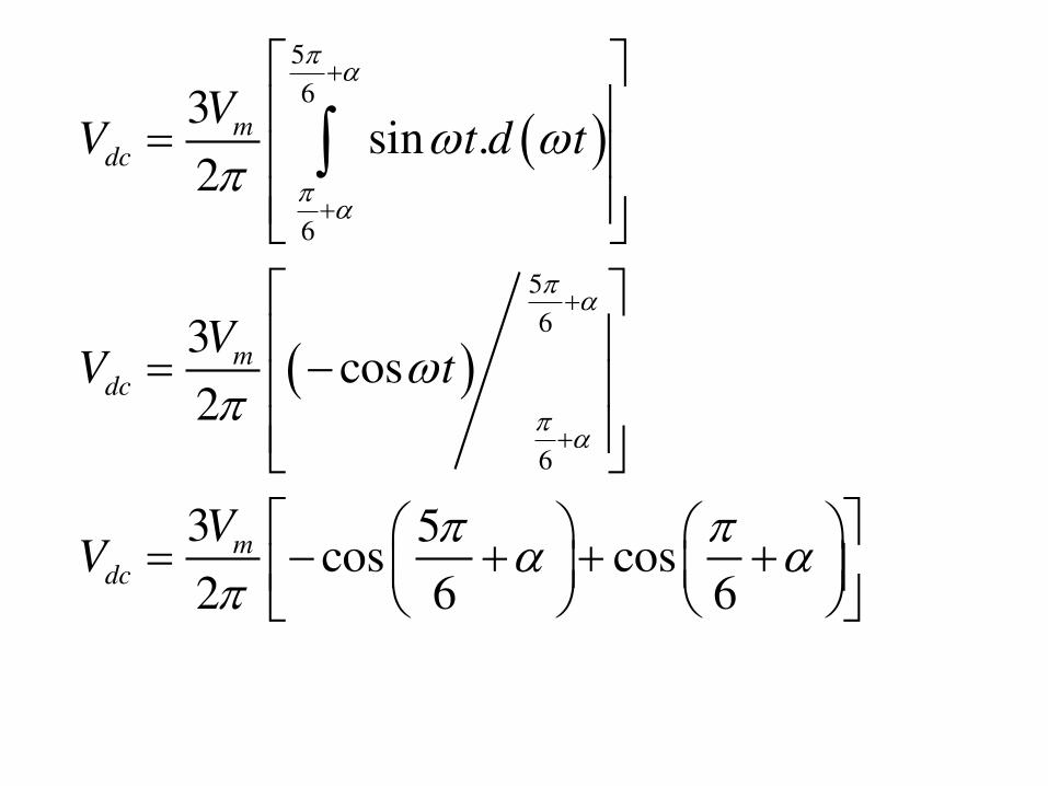
3sin .
2
3cos
2
3 5cos cos
2 6 6
mdc
mdc
mdc
VV t d t
VV t
VV

0 0
0
Note from the trigonometric relationship
cos cos .cos sin .sin
5 5cos cos sin sin
6 63
2co
cos 150 cos sin 150 sin3
2 cos 30
s .cos sin sin6 6
.cos
mdc
mdc
A
VV
B A B A B
VV
0sin 30 sin
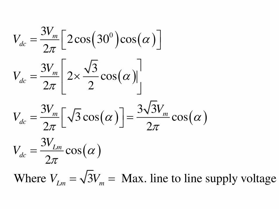
032cos 30 cos
2
3 32 cos
2 2
3 3 33 cos cos
2 2
3cos
2
Where 3 Max. line to line supply voltage
mdc
mdc
m mdc
Lmdc
Lm m
VV
VV
V VV
VV
V V
15 26
2 2
6
1
2
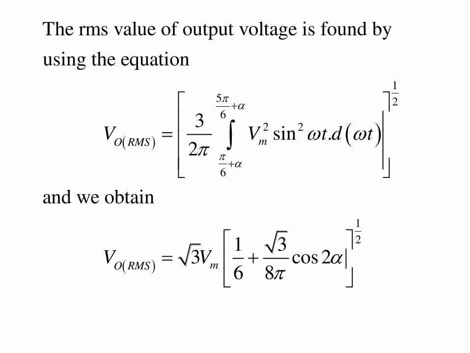
The rms value of output voltage is found by
using the equation
3sin .
2
and we obtain
1 33 cos 2
6 8
mO RMS
mO RMS
V V t d t
V V

3 Phase Half Wave
Controlled Rectifier Output
Voltage Waveforms For RL
Load
at
Different Trigger Angles

0
0
300
300
600
600
900
900
1200
1200
1500
1500
1800
1800
2100
2100
2400
2400
2700
2700
3000
3000
3300
3300
3600
3600
3900
3900
4200
4200
Van
V0
V0
Van
=300
=600
Vbn
Vbn
Vcn
Vcn
t
t
=300
=600

030
060
090
0120
0150
0180
0210
0240
0270
0300
0330
0360
0390
0420
0
V0
Van
=900
Vbn Vcn
t
=900

3 Phase Half Wave Controlled Rectifier With
R Load and
RL Load with FWD

a a
b b
c c
R
V0
L
R V0
+
T1
T2
T3
n n
T1
T2
T3

3 Phase Half Wave
Controlled Rectifier Output
Voltage Waveforms For R Load
or RL Load with FWD
at
Different Trigger Angles

0
0
300
300
600
600
900
900
1200
1200
1500
1500
1800
1800
2100
2100
2400
2400
2700
2700
3000
3000
3300
3300
3600
3600
3900
3900
4200
4200
Vs
V0
Van
=0
=150
Vbn Vcn
t
VanVbn Vcn
t
=00
=150

0
0
300
300
600
600
900
900
1200
1200
1500
1500
1800
1800
2100
2100
2400
2400
2700
2700
3000
3000
3300
3300
3600
3600
3900
3900
4200
4200
V0
=300
VanVbn Vcn
t
V0
=600
VanVbn Vcn
t
=300
=600

To Derive An
Expression For The Average Or Dc Output Voltage Of A
3 Phase Half Wave Converter With Resistive Load
Or RL Load With FWD
0
1
0 0
1
0
2
0 0
2
0
306
30 180 ;
sin
5 150
6
150 300 ;
sin 120
O an m
O bn m
T is triggered at t
T conducts from to
v v V t
T is triggered at t
T conducts from to
v v V t

0
3
0 0
3
0
0
7 270
6
270 420 ;
sin 240
sin 120
O cn m
m
T is triggered at t
T conducts from to
v v V t
V t

0
0
0
0
0
0
180
30
0 0
180
30
180
30
3.
2
sin ; for 30 to 180
3sin .
2
3sin .
2
dc O
O an m
dc m
mdc
V v d t
v v V t t
V V t d t
VV t d t
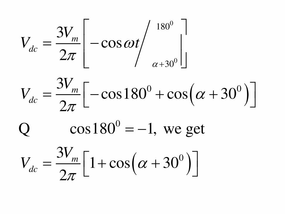
0
0
180
30
0 0
0
0
3cos
2
3cos180 cos 30
2
cos180 1, we get
31 cos 30
2
mdc
mdc
mdc
VV t
VV
VV
Q

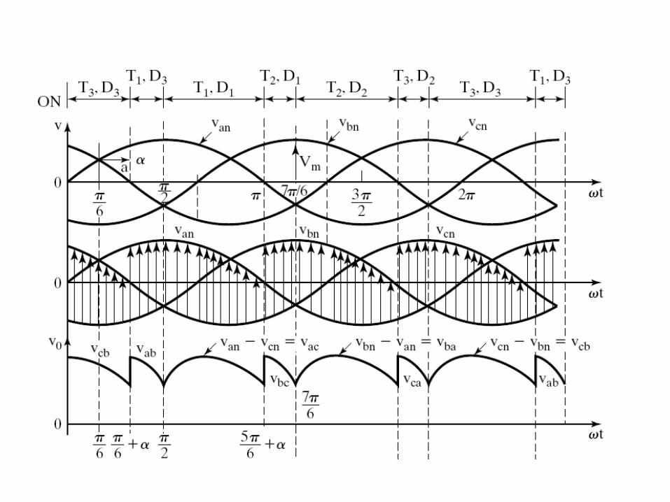
Three Phase Semiconverters
• 3 Phase semiconverters are used in Industrial dc drive applications upto 120kW
power output.
• Single quadrant operation is possible.
• Power factor decreases as the delay angle
increases.
• Power factor is better than that of 3 phase
half wave converter.
3 Phase
Half Controlled Bridge Converter
(Semi Converter)
with Highly Inductive Load &
Continuous Ripple free Load
Current
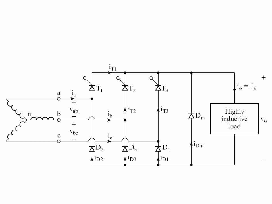

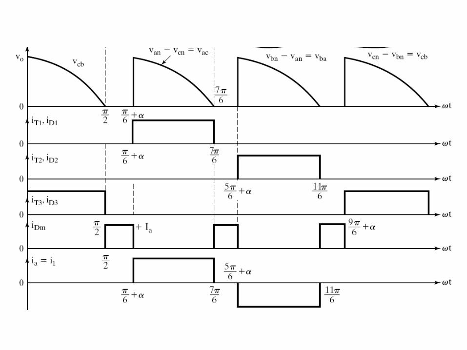
Wave forms of 3 Phase
Semiconverter for
> 600

0 0
1
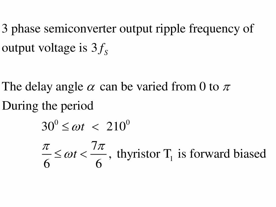
3 phase semiconverter output ripple frequency of
output voltage is 3
The delay angle can be varied from 0 to
During the period
30 210
7, thyristor T is forward biased
6 6
Sf
t
t

1
1 1
If thyristor is triggered at ,6
& conduct together and the line to line voltage
appears across the load.
7At , becomes negative & FWD conducts.
6
The load current contin
ac
ac m
T t
T D
v
t v D
1 1
ues to flow through FWD ;
and are turned off.
mD
T D

1
2
1 2
If FWD is not used the would continue to
conduct until the thyristor is triggered at
5, and Free wheeling action would
6
be accomplished through & .
If the delay angle , e3
mD T
T
t
T D
ach thyristor conducts
2for and the FWD does not conduct.
3mD
0
0
0
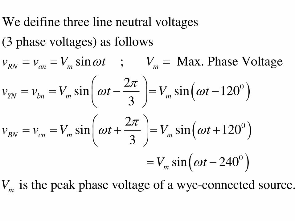
We deifine three line neutral voltages
(3 phase voltages) as follows
sin ; Max. Phase Voltage
2sin sin 120
3
2sin sin 120
3
sin 240
RN an m m
YN bn m m
BN cn m m
m
v v V t V
v v V t V t
v v V t V t
V t
V
is the peak phase voltage of a wye-connected source.m

3 sin6
53 sin
6
3 sin2
3 sin6
RB ac an cn m
YR ba bn an m
BY cb cn bn m
RY ab an bn m
v v v v V t
v v v v V t
v v v v V t
v v v v V t


To derive an
Expression for the
Average Output Voltage
of 3 Phase Semiconverter
for > / 3 and Discontinuous Output Voltage

76
6
76
6
For and discontinuous output voltage:3
the Average output voltage is found from
3.
2
33 sin
2 6
dc ac
dc m
V v d t
V V t d t

max
3 31 cos
2
31 cos
2
3 Max. value of line-to-line supply voltage
The maximum average output voltage that occurs at
a delay angle of 0 is
3 3
mdc
mLdc
mL m
mdmdc
VV
VV
V V
VV V
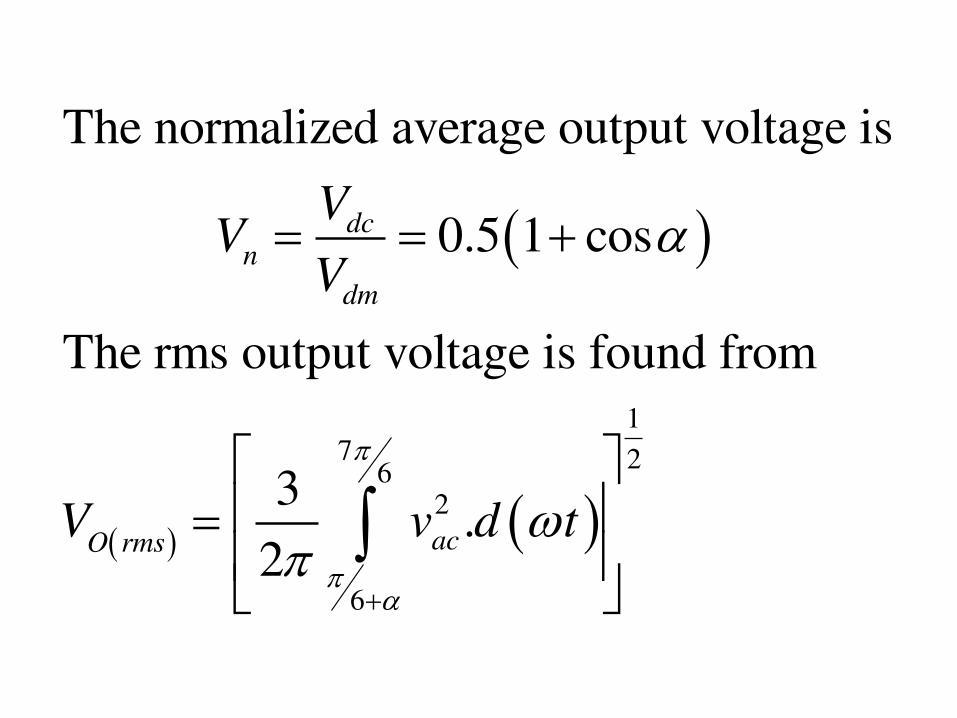
17 2
62
6
The normalized average output voltage is
0.5 1 cos
The rms output voltage is found from
3.
2
dcn
dm
acO rms
VV
V
V v d t

Three Phase Dual Converters
• For four quadrant operation in many industrial
variable speed dc drives , 3 phase dual
converters are used.
• Used for applications up to 2 mega watt output
power level.
• Dual converter consists of two 3 phase full
converters which are connected in parallel & in
opposite directions across a common load.
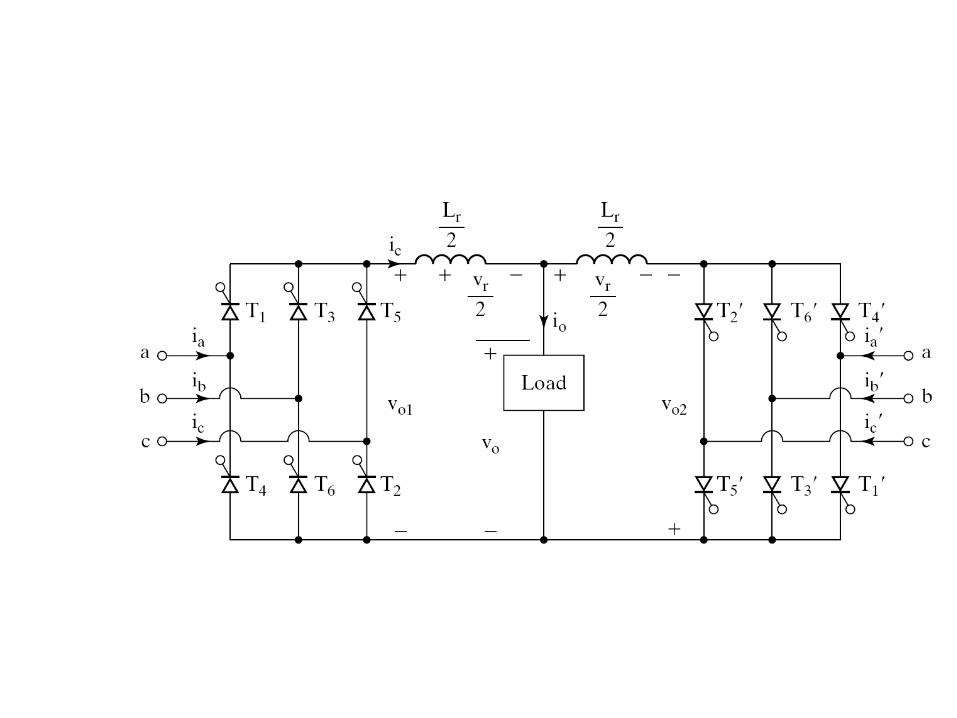
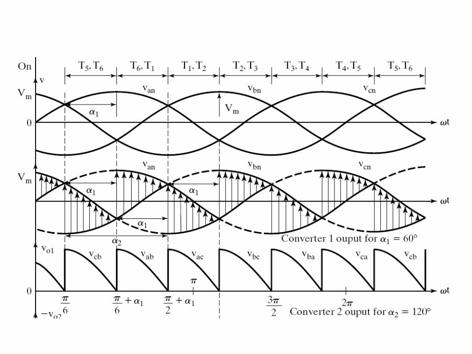


Four Quadrant Operation

Introduction • Chopper is a static device.
• A variable dc voltage is obtained from a constant dc voltage source.
• Also known as dc-to-dc converter.
• Widely used for motor control.
• Also used in regenerative braking.
• Thyristor converter offers greater efficiency, faster response, lower maintenance, smaller size and smooth
control.
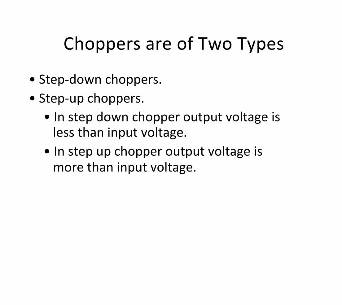
Choppers are of Two Types
• Step-down choppers.
• Step-up choppers.
• In step down chopper output voltage is less than input voltage.
• In step up chopper output voltage is
more than input voltage.

Principle Of
Step-down Chopper
Chopper
i0 +
V V0 R
-

• A step-down chopper with resistive load.
• The thyristor in the circuit acts as a switch.
• When thyristor is ON, supply voltage appears across the load
• When thyristor is OFF, the voltage across
the load will be zero.
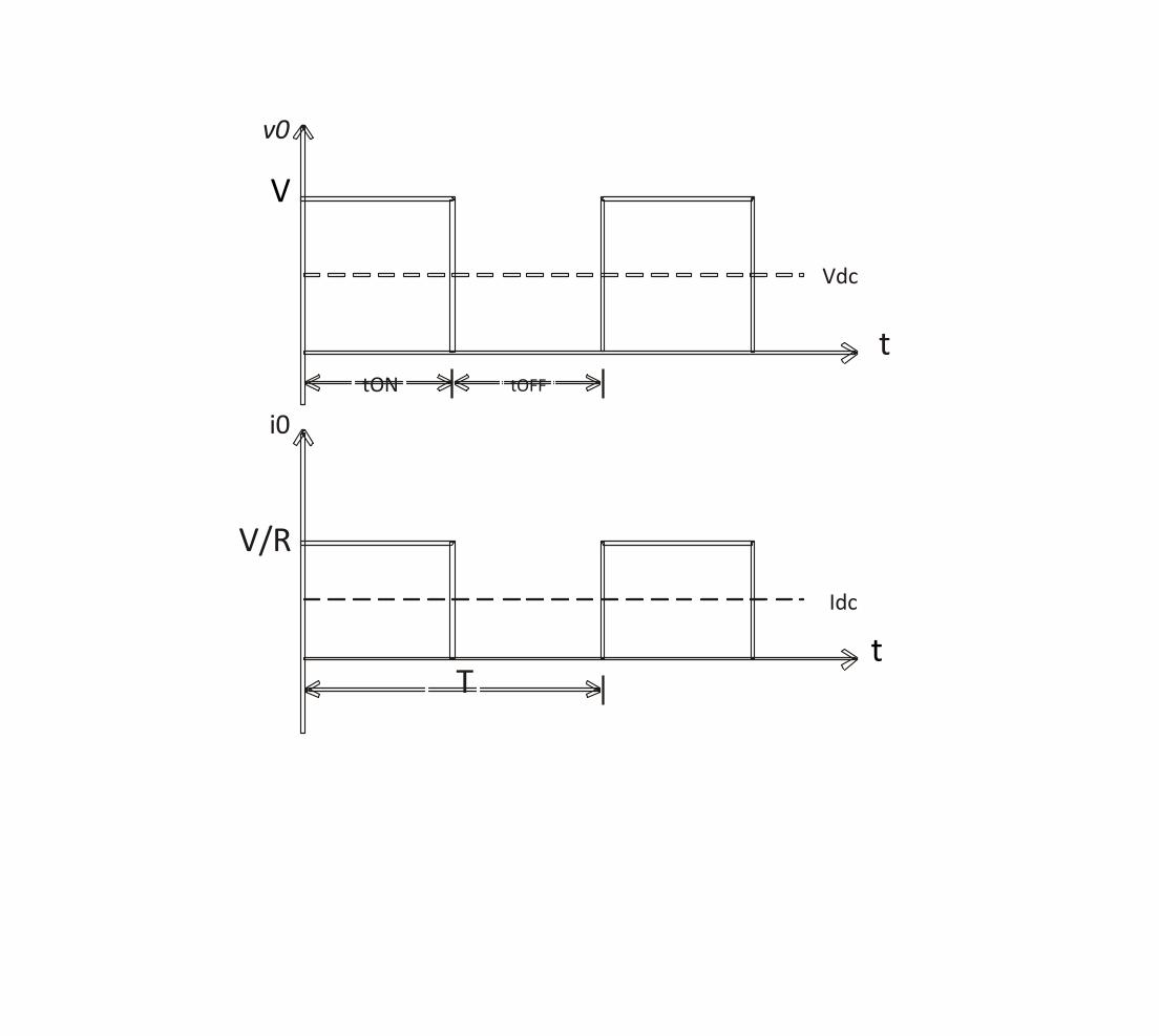
v0
V
Vdc
t tON tOFF
i0
V/R
Idc
t T
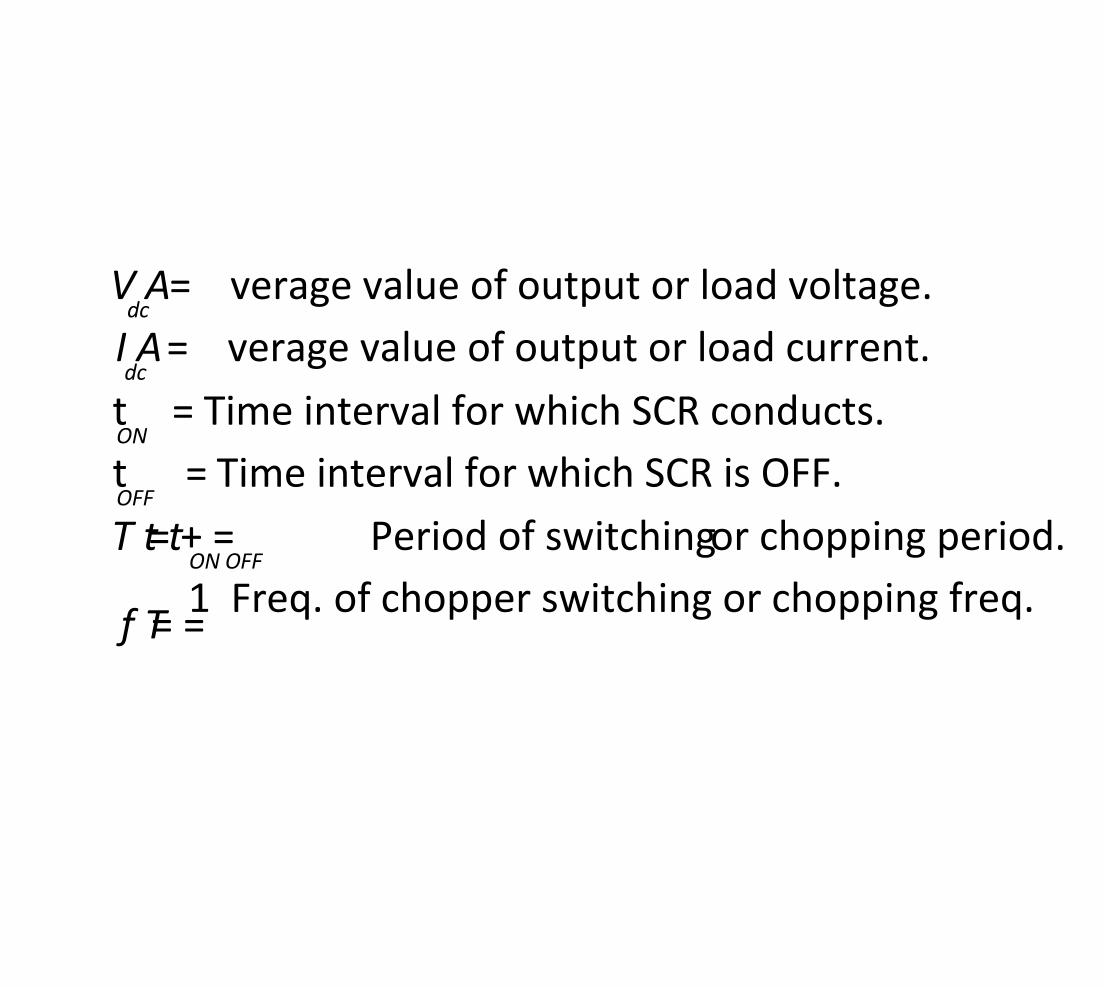
verage value of output or load voltage. V A = dc
verage value of output or load current. I A = dc
Time interval for which SCR conducts. t = ON
Time interval for which SCR is OFF. t = OFF
Period of switching T t t = + = or chopping period. ON OFF
1 Freq. of chopper switching or chopping freq. f T = =

Average Output Voltage
t V V t t = ON
+ dc
ON OFF
t . V V V d = = ON
T dc
t duty cycle but d = = ON
t

Average Output Current
V I R = dc dc
t V V I d = = ON
R T R dc
RMS value of output voltage
t
V v dt = 1 ON 2
T O o
0

But during , t v V = ON o
Therefore RMS output voltage
1 t ON
V V dt = 2
T O
0
t V 2
. V t V = = ON
T T O ON
. V d V = O
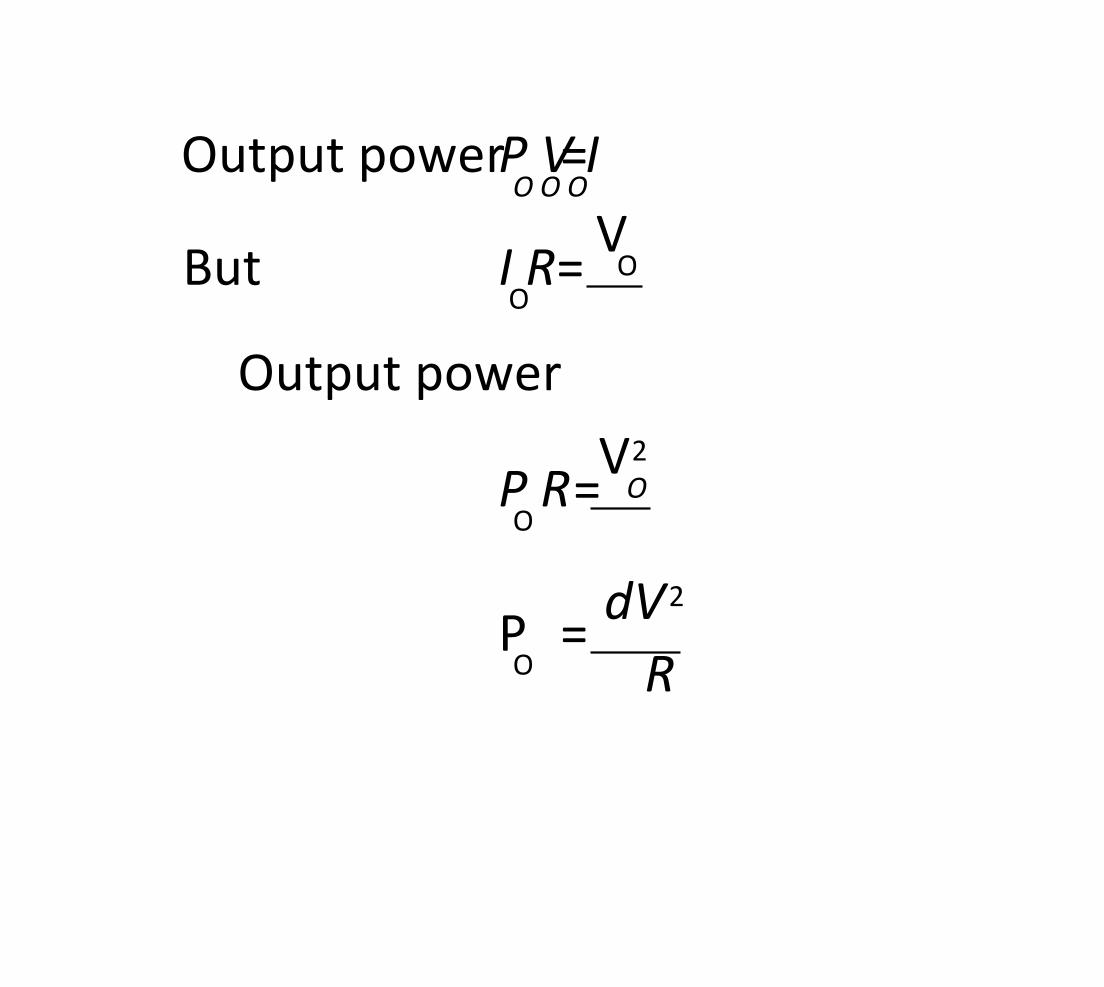
Output power P V I = O O O
V But I R = O
O
Output power
V 2
P R = O O
dV 2
P = R O
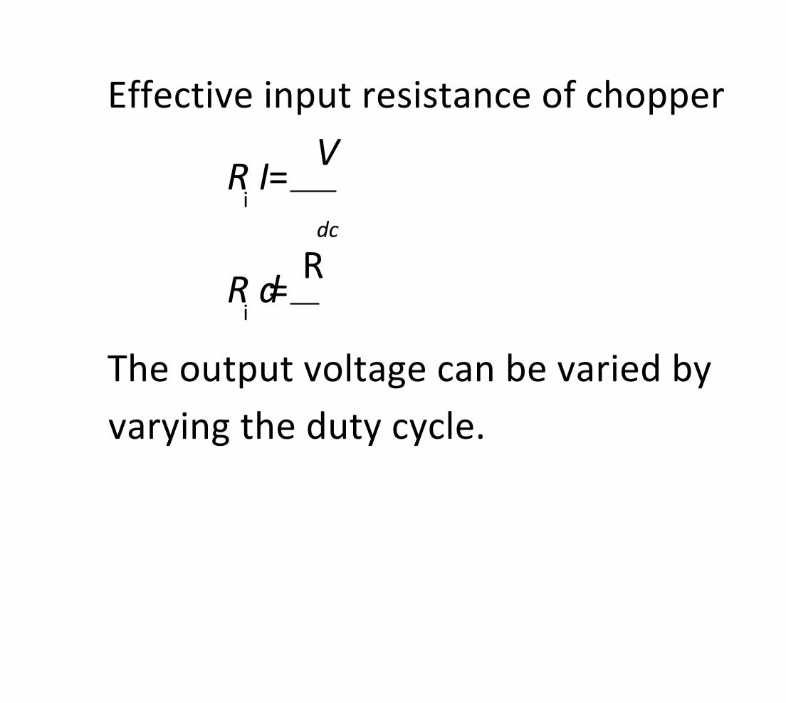
Effective input resistance of chopper
V R I =
i
dc
R R d =
i
The output voltage can be varied by
varying the duty cycle.

Methods Of Control
• The output dc voltage can be varied by the following methods.
– Pulse width modulation control or
constant frequency operation.
– Variable frequency control.

Pulse Width Modulation
• tON is varied keeping chopping frequency
f & chopping pe iod T constant. • Output voltage is varied by varying the ON
time tON

V0
V
tON tOFF
t T
V0
V
t
tON tOFF
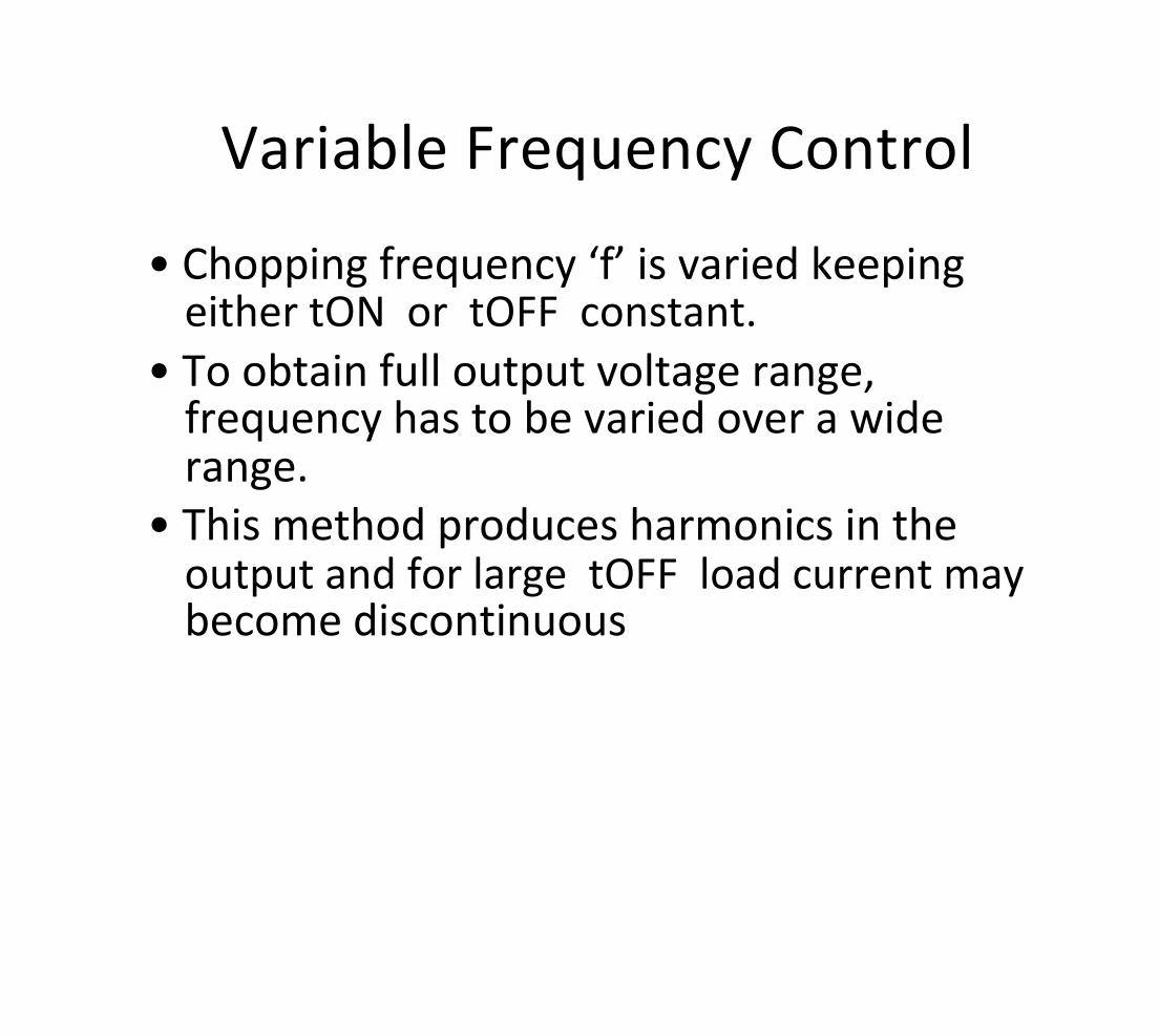
Variable Frequency Control
• Chopping f e uency f is va ied keeping either tON or tOFF constant.
• To obtain full output voltage range, frequency has to be varied over a wide range.
• This method produces harmonics in the output and for large tOFF load current may become discontinuous

v0
V
tON tOFF
t
T v0
V
tON tOFF
t T
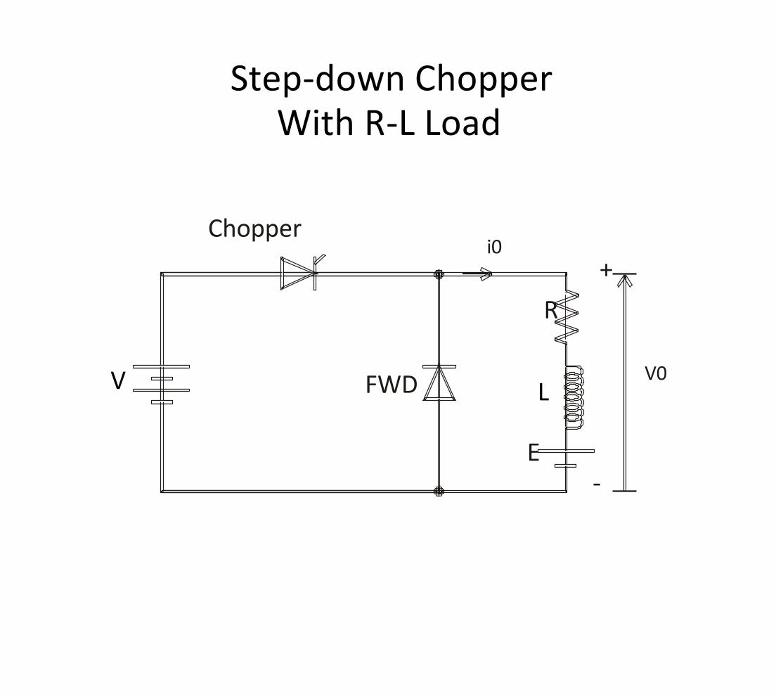
Step-down Chopper
With R-L Load
Chopper i0
+
R
V0 V FWD L
E
-

• When chopper is ON, supply is connected across load.
• Current flows from supply to load.
• When chopper is OFF, load current continues to flow in the same direction through FWD due to energy stored in inducto L .
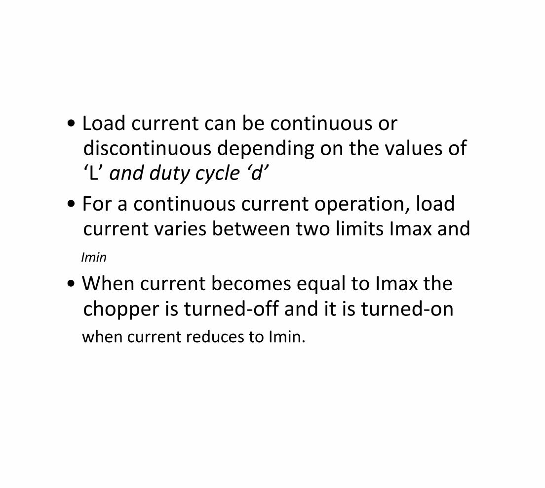
• Load current can be continuous or discontinuous depending on the values of L and duty cycle d
• For a continuous current operation, load current varies between two limits Imax and
Imin
• When current becomes equal to Imax the
chopper is turned-off and it is turned-on
when current reduces to Imin.

v0 Output voltage
V
tON T tOFF
t
Output i0
current Imax
Continuous current Imin
t Output i0 current
Discontinuous current
t
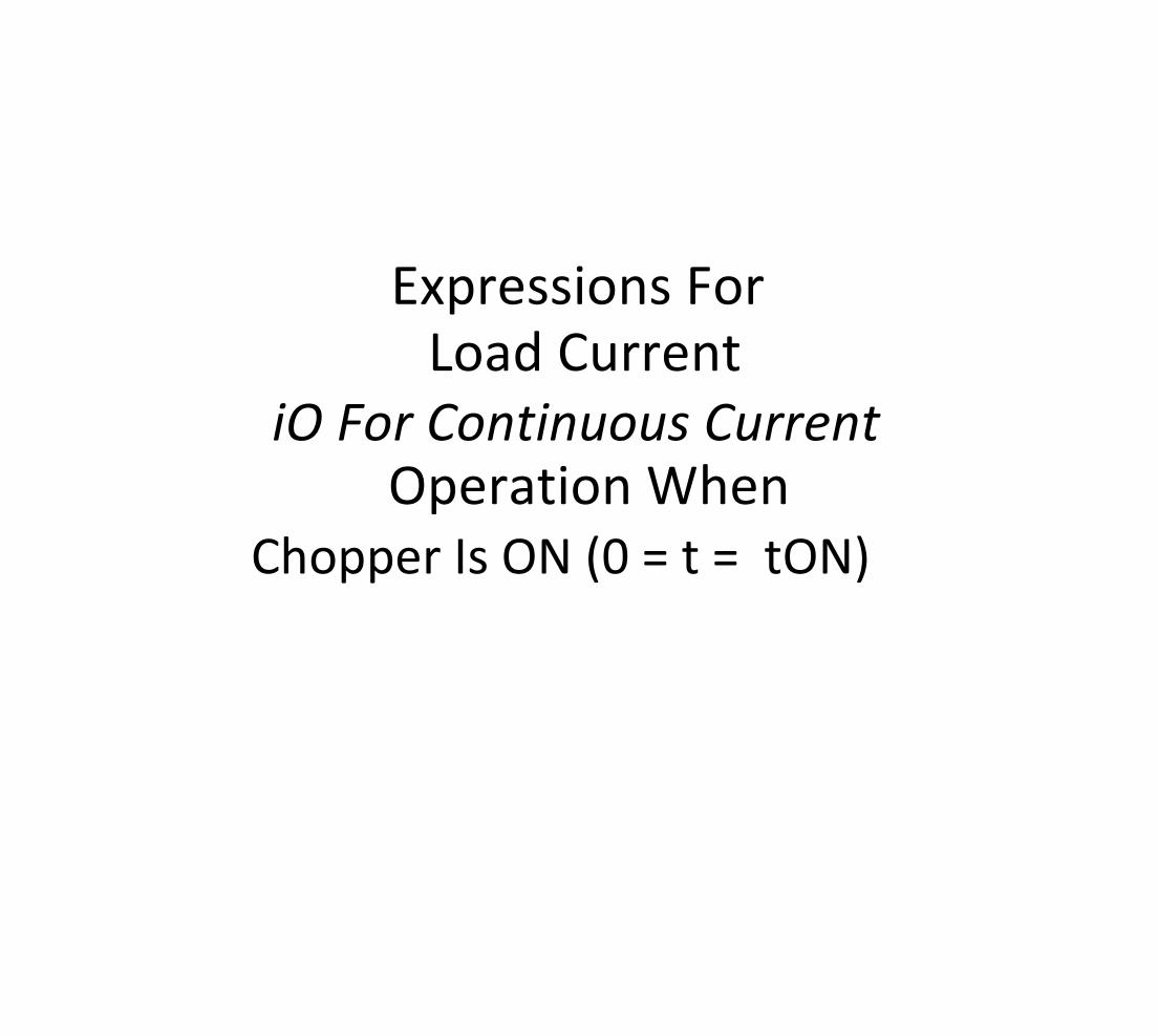
Expressions For
Load Current
iO For Continuous Current Operation When
Chopper Is ON (0 = t = tON)

i0 +
R
V0 V L
E
-

di V i R L E = + + O
dt O
Taking Laplace Transform
V E ( ) ( ) ( ) . 0 RI S L S I S i = + - + -
S S O O O
( ) At 0, initial current 0 t i I = = - min O
I V E - ( ) I S = + min
R R S O
+ LS S + L L

Taking Inverse Laplace Transform
R R V E - ( ) t t - -
1 i t e I e = - + L L
R min O
This expression is valid for 0 , t t = = ON
i.e., during the period chopper is ON.
At the instant the chopper is turned off,
load c urrent is i t I = ( ) max O ON

When Chopper is OFF
i0
R
L
E

( ) When Chopper is OFF 0 t t = = OFF
di 0 Ri L E = + + O
dt O
Talking Laplace transform
( ) ( ) E ( ) 0 0 RI S L SI S i = + - + -
S O O O
Redefining time origin we have at 0, t =
initial current 0 i I = - ( ) max O

I E ( ) I S = - max
R R O
S + LS S + L L
Taking Inverse Laplace Transform
E R R
( ) t t - - 1 i t I e e = - - L L
R max O
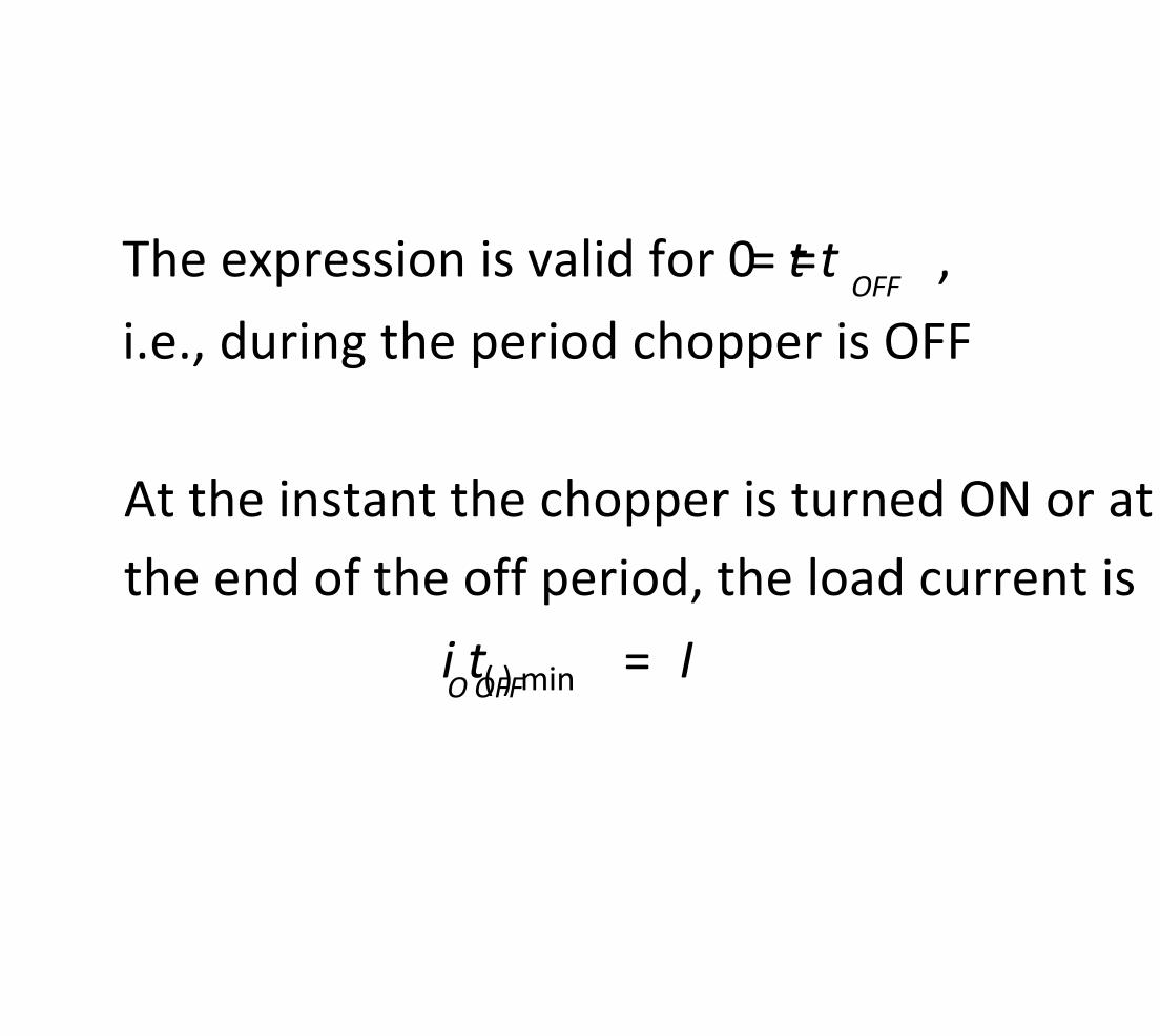
The expression is valid for 0 , t t = = OFF
i.e., during the period chopper is OFF
At the instant the chopper is turned ON or at
the end of the off period, the load current is
i t I = ( ) min O OFF

To Find & I I max min
From equation
R R V E - ( )
t t - -
1 i t e I e = - + L L
R min O
( ) At , t t dT i t I = = = max ON O
V E - dRT dRT - -
1 I e I e = - + L L
R max min

From equation
E R R
( ) t t - - 1 i t I e e = - - L L
R max O
( ) At , t t T t i t I = = - = min OFF ON O
( ) 1 t t d T = = - OFF
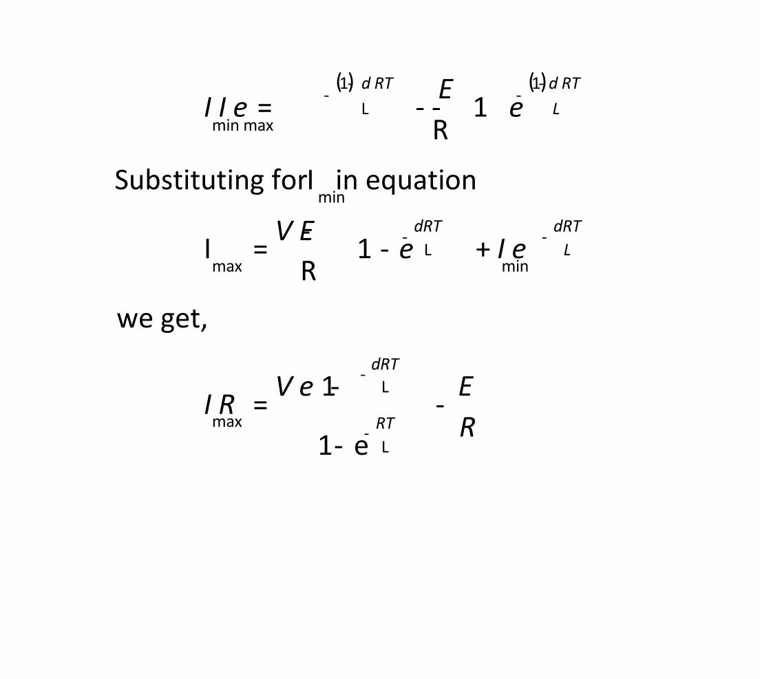
( ) ( ) E 1 1 d RT d RT - - - -
1 I I e e = - - L L
R min max
Substituting for in equation I min
V E - dRT dRT - -
1 I e I e = - + L L
R max min
we get,
dRT -
1 V e E - L
I R = - R max RT
- 1 e - L

Substituting for in equation I max
( ) ( ) E 1 1 d RT d RT - - - -
1 I I e e = - - L L
R min max
we get,
dRT
1 V e E - L
I R = - R min RT
1 e - L
( ) is known as the steady state ripple. I I - max min

Therefore peak-to-peak ripple current
I I I = - max min
Average output voltage
. V d V = dc
Average output current
I I + I = max min
( ) 2 dc approx

Assuming load current varies linearly
from to instantaneous I I min max
load current is given by
( ) . 0 I t ( ) i I for t t dT = + = =
dT min O ON
I I - i I t = + max min
dT min O
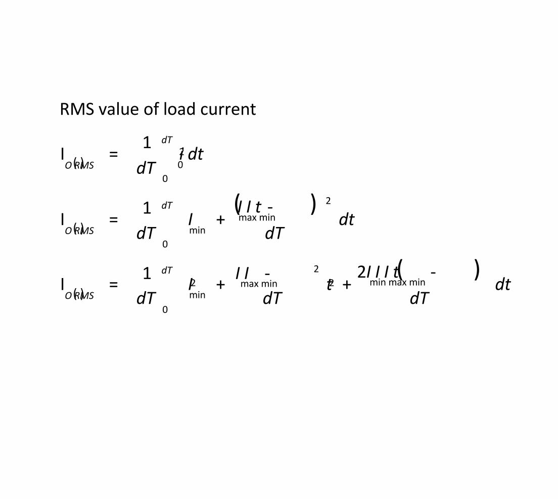
RMS value of load current
1 dT
I i dt = 2 ( ) dT 0 O RMS
0
( ) 2 I I t - 1 dT
I I dt = + max min ( ) dT dT min O RMS
0
( ) 2 I I I t - 1 I I - 2 dT
I I t dt = + + min max min 2 2 max min ( ) dT dT dT min O RMS
0
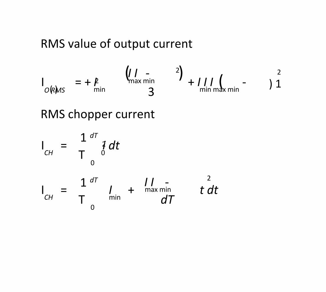
RMS value of output current
( ) I I - 2 2
( I I I I I = + + - ) 1 max min 2
( ) 3 min min max min O RMS
RMS chopper current
1 dT
I i dt = 2
T 0 CH
0
2 I I - 1 dT
I I t dt = + max min
T dT min CH
0

1
( ) I I - 2 2
( ) I d I I I I = + + - max min 2
3 min min max min CH
I d I = ( ) CH O RMS
Effective input resistance is
V R I =
i
S
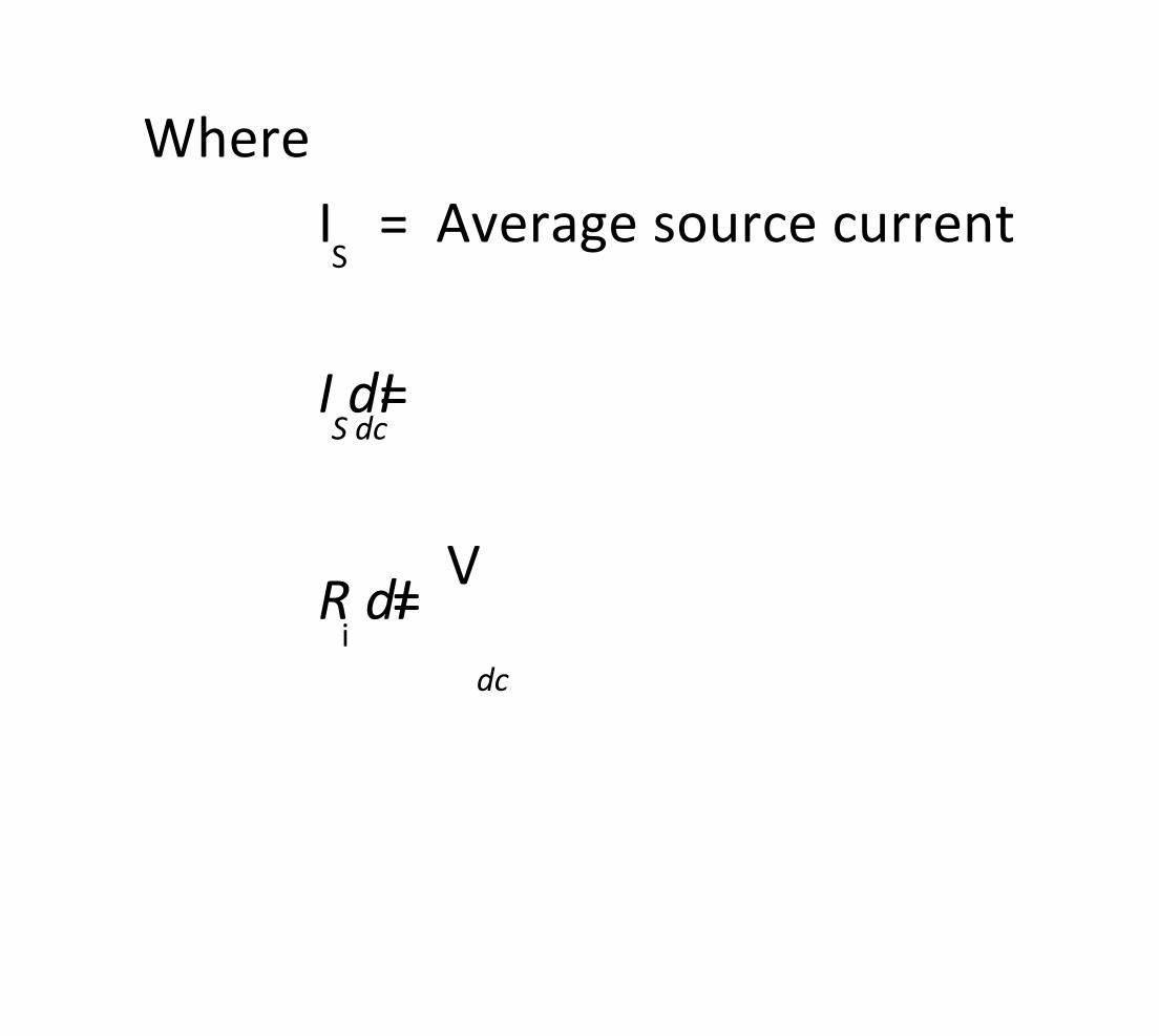
Where
Average source current I = S
I dI = S dc
V R dI =
i
dc

Principle Of Step-up Chopper
L I D
+ + -
L O C V VO A D
Chopper
-
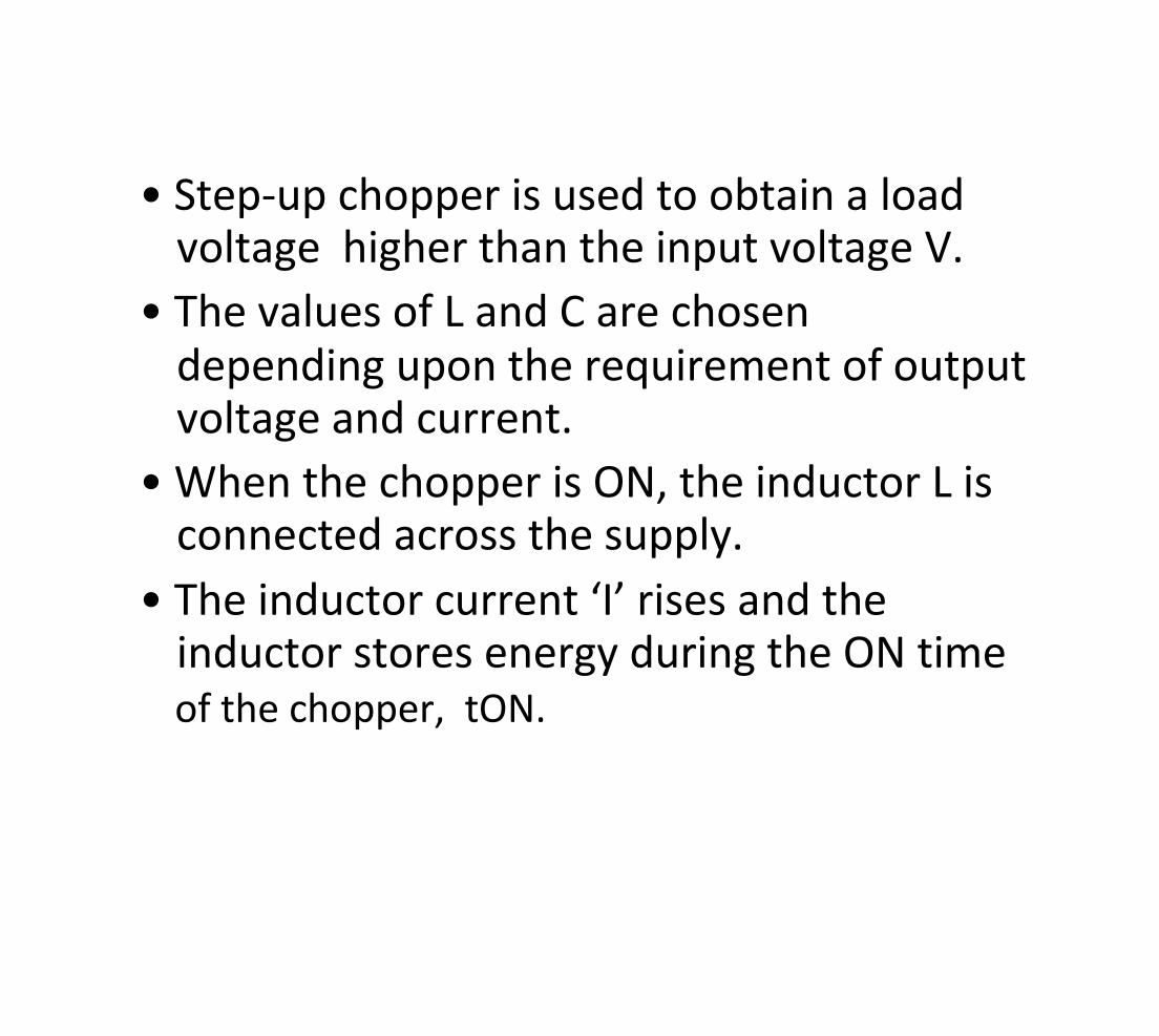
• Step-up chopper is used to obtain a load voltage higher than the input voltage V.
• The values of L and C are chosen
depending upon the requirement of output voltage and current.
• When the chopper is ON, the inductor L is connected across the supply.
• The inducto cu ent I ises and the inductor stores energy during the ON time
of the chopper, tON.

• When the chopper is off, the inductor current I is forced to flow through the diode D and load for a period, tOFF.
• The current tends to decrease resulting in reversing the polarity of induced EMF in L.
• Therefore voltage across load is given by
dI . ., V V L i e V V = + >
dt O O
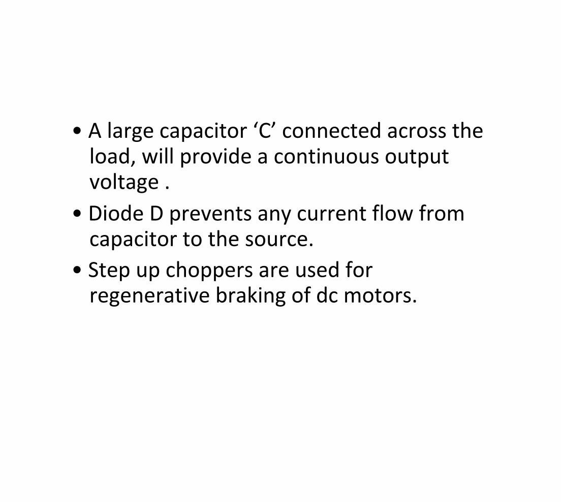
• A la ge capacito C connected ac oss the load, will provide a continuous output voltage .
• Diode D prevents any current flow from capacitor to the source.
• Step up choppers are used for regenerative braking of dc motors.
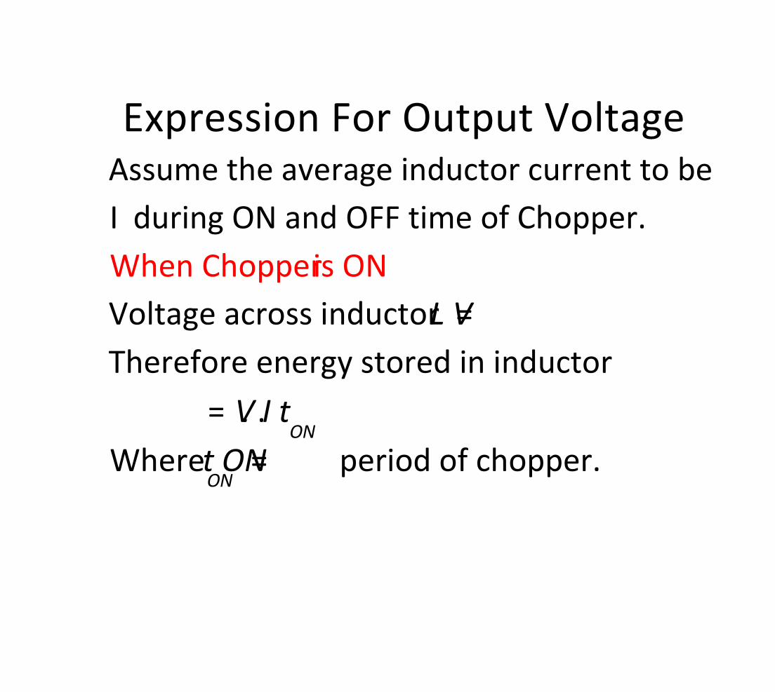
Expression For Output Voltage Assume the average inductor current to be
during ON and OFF time of Chopper. I
When Chopper is ON
Voltage across inductor L V =
Therefore energy stored in inductor
= . . V I t ON
Where period of chopper. t ON = ON

When Chopper is OFF
(energy is supplied by inductor to load)
Voltage across L V V = - O
( ) Energy supplied by inductor L V V It = - O OFF
where period of Chopper. t OFF = OFF
Neg lecting losses, energy stored in inductor
L = energy supplied by inductor L

( ) VIt V V It = - ON O OFF
[ ] V t t + V = ON OFF
t O
OFF
T V V T t =
- O
ON
Where
T = Chopping period or period
of switching.

T t t = + ON OFF
1 V V t =
O
1 - ON
T
1 V V d = -
1 O
t Where duty cyle d T = = ON

For variation of duty cycle ' ' in the d
range of 0 1 the output voltage d V < < O
will vary in the range V V < < 8 O

INTRODUCTION
AC voltage controllers are thyristor based devices which convert fixed alternating voltage directly to variable alternating voltage without change in frequency.
Using these controllers, rms value of the voltage across the load is steplessly varied from a maximum value to zero.
The simplest way to control AC voltage to the load is by using AC switch (bidirectional).
The bi-directional conducting property can be achieved by simply connecting two unidirectional thyristors in inverse parallel to each other.
AC voltage controllers are naturally commutated. 1

AC POWER CONTROL
Control of AC voltage controllers is of two
kinds.
1. On-Off Control (Integral Cycle Control)
2. Phase Control
2
Single Phase AC voltage Controller

1- On-Off Control (Integral Cycle Control)
The load power can be controlled by connecting the source to
the load for few complete cycles then disconnecting the
source from the load for another number of cycles, and
repeating the switching cycle.
Suitable for systems with large time constants.
Average power to the load can be varied from 0% through
100%
Integral cycle control finds applications in heating loads and
for motor speed control.
(In industry, there are several applications in which mechanical time constant
or thermal time constant is of the order of several seconds. For example,
mechanical time constant for many of the speed-control drives, or thermal
time constants for most of the heating loads is usually quite high. For such
applications, almost no variation in speed or temperature will be noticed if
control is achieved connecting the load to source for some on cycles and then
disconnecting the load for some off cycles.)
3

4
For resistive load
Voltage
across thyristors
2 2
1 1
T
T
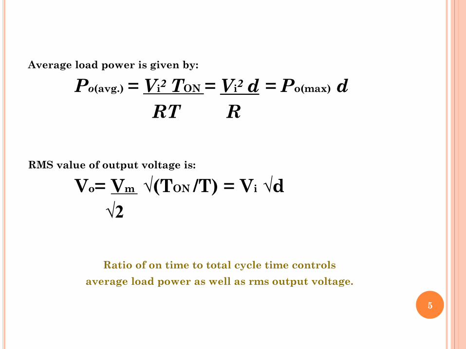
Average load power is given by:
Po(avg.) = Vi² TON = Vi² d = Po(max) d
RT R
RMS value of output voltage is:
Vo= Vm √(TON /T) = Vi √d
√2
Ratio of on time to total cycle time controls
average load power as well as rms output voltage.
5
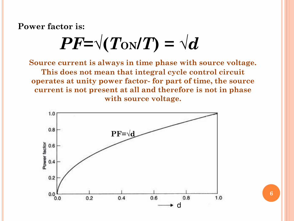
Power factor is:
PF=√(TON/T) = √d Source current is always in time phase with source voltage.
This does not mean that integral cycle control circuit
operates at unity power factor- for part of time, the source
current is not present at all and therefore is not in phase
with source voltage.
6
d
PF=√d

2- AC Phase Control Phase control is kind in which thyristors are fired once every
cycle and the instant of firing can be delayed from the zero
crossing. By this, only a part of the voltage waveform appears
across the load, providing voltage control. The load current
appears in pulses, the zero crossing of which can be used for
turn-off of the thyristors.
Suitable for loads with short time constants.
Firing instants of thyristors are 180° apart, each occuring in
its respective half cycle.
By controlling this instant of firing, the effective voltage
occuring across the load can be varied.
As the two thyristors have firing pulses delayed by 180° , the
AC current pulses are periodic and symmetrical and there is
no DC current component. The load voltage also does not have
any DC component.
7

8
Single-phase AC voltage controller with resistive load
Load power can be
varied by changing α
over the full range from zero to 180°
9
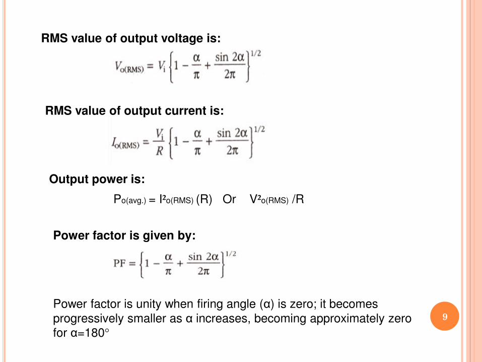
RMS value of output voltage is:
RMS value of output current is:
Output power is:
Po(avg.) = I²o(RMS) (R) Or V²o(RMS) /R
Power factor is given by:
Power factor is unity when firing angle (α) is zero; it becomes
progressively smaller as α increases, becoming approximately zero for α=180°

10
Variation of output voltage and power
With delay angle for resistive load
11
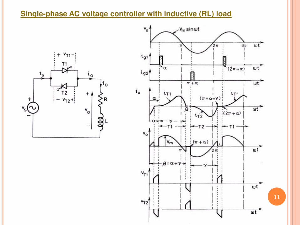
Single-phase AC voltage controller with inductive (RL) load

CYCLOCONVERTERS
12

INTRODUCTION Cycloconverter is frequency changer that converts AC power at one input
frequency to AC output power at a different frequency.
Variable frequency output can be obtained by AC DC AC using phase-
controlled converters (rectifier followed by inverter). This is two stage
frequency conversion.
Single-stage frequency conversion is called cycloconversion.
Cycloconversion can be anyone of following:
1- conversion of variable frequency to fixed one (aircraft or shipboard power
supplies or wind generators)
2- conversion of fixed frequency to a variable one (AC motor speed control)
Cycloconverters can be step-up or step-down
For efficient operation, cycloconverters are usually operated in frequency
range of zero to less than one-third the source frequency.
13