
EE 110 – Basic Electronics -...
49
EE‐110 – Basic Electronics EE 110 Basic Electronics Bipolar Junction Transistor (BJT) ‐ Introduction Introduction
Transcript of EE 110 – Basic Electronics -...

EE‐110 – Basic ElectronicsEE 110 Basic Electronics
Bipolar Junction Transistor (BJT)
‐ IntroductionIntroduction

SubtopicsSubtopics
3 0 Bipolar Junction Transistors (6 Hours)3.0 Bipolar Junction Transistors (6 Hours)
3 1 T i t t ti d ti3.1 Transistor construction and operation
3.2 Transistor configuration
3.3 Transistor datasheet and terminal identification

IntroductionIntroduction
• Bipolar means there are two polarities involve in this transistor when operating
• The polarities are the carries involve in theThe polarities are the carries involve in the operation of the transistor: holes and electronselectrons
• If only one carrier is employed (holes or electrons) it is said to be unipolar (ex: Diode)electrons), it is said to be unipolar (ex: Diode)

IntroductionIntroduction• BJT is a three‐layer semiconductor• Two types of BJT
– pnp: − npn:
– E = emitter, B = base, C = collector

Transistor ConstructionTransistor Construction
• Layer width:Layer width:– outer layer >> inner layer
• Doping• Doping:– emitter layer is highly doped (more conductivity)
( )– collector layer is lightly doped (less conductivity)
– base layer is more lightly doped (lesser d ti it )conductivity)
– doping: E > C > B

Transistor OperationTransistor Operation
• The operation of pnp and npn are the sameThe operation of pnp and npn are the same except for the current flow
For pnp:– For pnp:
• Current flow from E to B and C
– For npn:
• Current flow from B and C to E
• As for that, both type will have the current equation:equation:
CBE III +=

Transistor OperationTransistor Operation• Proper biasing for pnp and npn transistor:
–pnp ‐ npn
This proper biasing is for transistor– This proper biasing is for transistor operation in active region (will be discussed in DC biasing)discussed in DC biasing)

Transistor Operation• Examine the pnp transistor for its forward
• It is very similar to a forward‐biased diodetransistor for its forward
biased junction at terminal E to B:
• Majority carrier (holes) flows from E to B
• Minority carrier (electrons) flows from B to E
• Resulting in small depletion region
• This means that the current flows heavily from E to B
Transistor OperationTransistor Operation
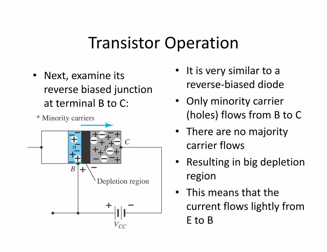
• Next, examine its • It is very similar to a Next, examine its reverse biased junction at terminal B to C:
reverse‐biased diode
• Only minority carrier (holes) flows from B to C
• There are no majority i flcarrier flows
• Resulting in big depletion iregion
• This means that the current flows lightly fromcurrent flows lightly from E to B
Transistor Operation
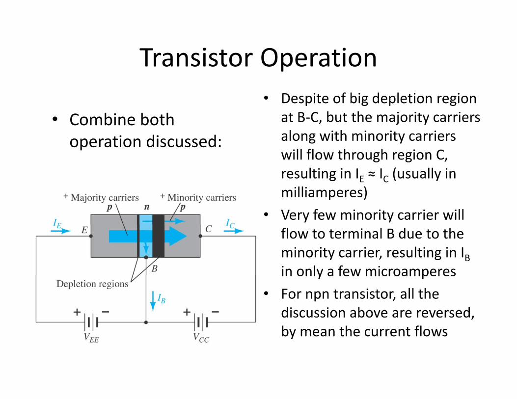
• Combine both• Despite of big depletion region
at B‐C, but the majority carriers Combine both operation discussed:
, j yalong with minority carriers will flow through region C, resulting in I ≈ I (usually inresulting in IE ≈ IC (usually in milliamperes)
• Very few minority carrier will flow to terminal B due to the minority carrier, resulting in IBin only a few microamperesin only a few microamperes
• For npn transistor, all the discussion above are reversed, by mean the current flows

Transistor ConfigurationTransistor Configuration• There are three commonly used configuration in BJT– Common‐base (CB) configuration
– Common‐emitter (CE) configuration
– Common‐collector (CC) configuration
• Further on, these configuration will be discussed on npn transistor first, the pnp d scussed o p t a s sto st, t e p ptransistor is the exact reverse (in means of current flows) of the npn transistor) p

CB ConfigurationCB Configuration
• By applying the proper biasing and grounding the base terminal:

CB ConfigurationCB Configuration• In CB configuration, the input terminal is between terminal E and B (due to ground atbetween terminal E and B (due to ground at B)
h l f d b l• The output terminal is fixed between terminal C and B
+− VBEinput output+− VCB
p
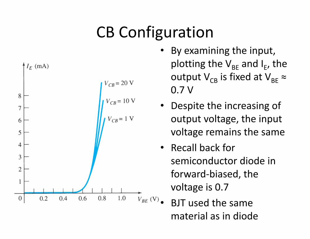
CB Configuration• By examining the input, plotting the VBE and IE, the
t t V i fi d t Voutput VCB is fixed at VBE ≈ 0.7 V
• Despite the increasing of• Despite the increasing of output voltage, the input voltage remains the samevoltage remains the same
• Recall back for semiconductor diode in forward‐biased, the voltage is 0.7
• BJT used the same material as in diode

CB ConfigurationCB Configuration• Examine the output at terminal C and B:

CB ConfigurationCB Configuration
• There are 3 region of operation:There are 3 region of operation:
–Active region
C ff i–Cutoff region
– Saturation region
• In active region, there’s a relation between IE and IC (this is only approximation):( y pp )
CE II ≅

CB ConfigurationCB Configuration
• In cutoff region output (collector) current isIn cutoff region, output (collector) current is zero (open‐circuit equivalent):
A 0=CI
• In saturation region, output (collector‐base) voltage is zero (short‐circuit equivalent):
V 0=CBV

Alpha (α)Alpha (α)
• By assuming IE = IC, it is assumed that IB = y g ,0, even though IB is in microamperes (this is only approximation)y pp )
• For the exact value (IB ≠ 0), the emitter and collector current will be:collector current will be:
EC II α=
• The value of α is below 1 but near 1 (range
EC
0.90 to 0.998)

Problem 3.13Problem 3.13• Question:
– By using the characteristic given,
a) Determine the collector current if IE = )4.5 mA and VCB = 4 V
b)Determine the collector current if IE =b)Determine the collector current if IE 4.5 mA and VCB = 16 V
c) How have the change in VCB affected thec) How have the change in VCB affected the resulting level of IC
d)O i t b i h IE dd)On an approximate basis, how are IE and IC related?

Problem 3.13Problem 3.13

Problem 3.13Problem 3.13
• Solution:
a) For IE = 4.5 mA and VCB = 4 V, IC = 4.5 mA
b) For IE 4 5 mA and VCB 16 V IC 4 5 mAb) For IE = 4.5 mA and VCB = 16 V, IC = 4.5 mA
c) Negligible (not change – not depend on )voltage)
d) IE = IC
Problem 3.15Problem 3.15
• Question:Question:
a) Given α = 0.998, determine IC if IE = 4 mA
b) i if 2 8 d 20b) Determine α if IE = 2.8 mA and IB = 20 μA

Problem 3.15Problem 3.15
• Solution:Solution:
a)
b)mA 993.3)4)(998.0( === mII EC α
b)
mA7822082 =−=−=∴+=
mIIIIII BCE
μ mA78.2208.2 =−=−=∴ mIII BEC μ
9929078.2∴
=mI
II
C
EC α
9929.08.2
===∴mIE
Cα
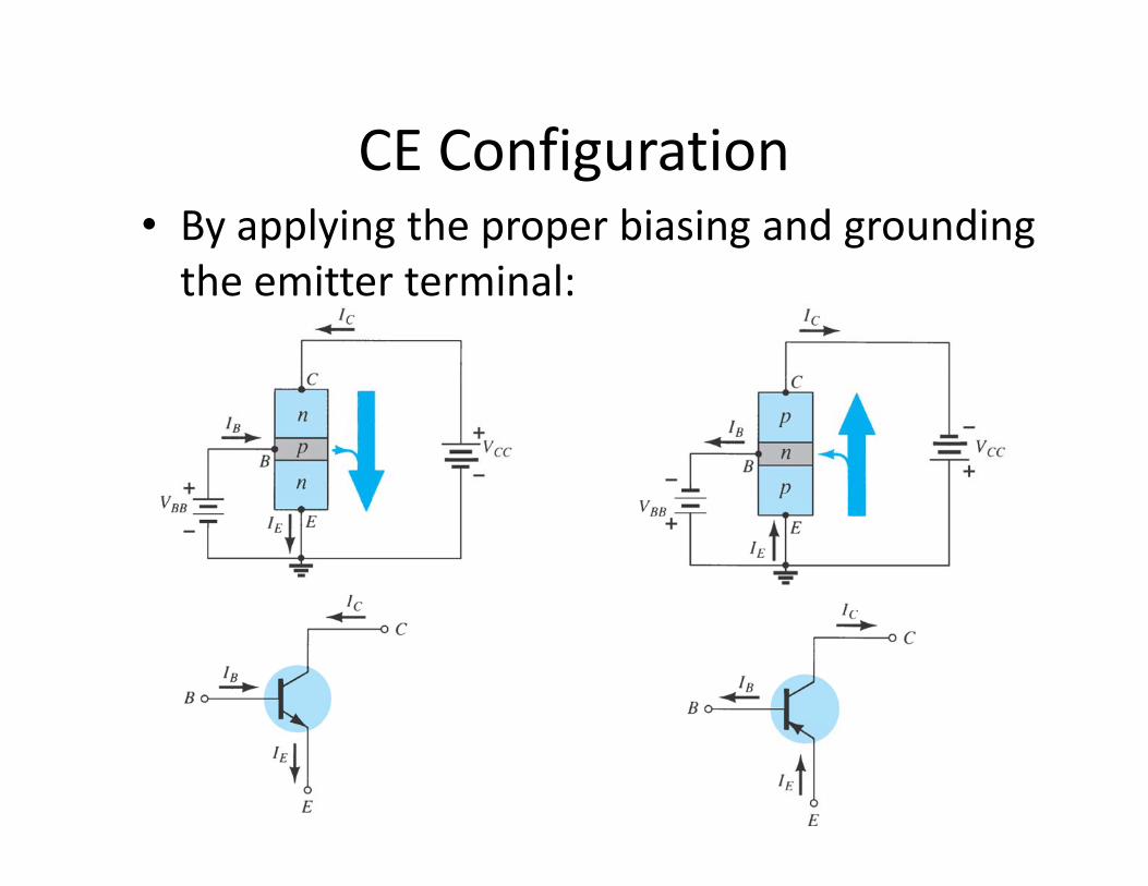
CE ConfigurationCE Configuration• By applying the proper biasing and grounding the emitter terminal:the emitter terminal:

CE ConfigurationCE Configuration• In CE configuration, the input terminal is between terminal B and E (due to ground atbetween terminal B and E (due to ground at E)
• The o tp t terminal is fi ed bet een terminal• The output terminal is fixed between terminal C and E
+ output
+−VBE
VCEinput
−

CE Configurationg
• By examining the i l i h VBEinput, plotting the VBE and IB, the output VCE is fixed at VBE ≈ 0 7 Vis fixed at VBE ≈ 0.7 V remains the same
• VBE = 0 7 V is appliedVBE 0.7 V is applied to all transistor configuration including this CE configuration
• VEB = 0.7 V for pnp transistor

CE ConfigurationE i h i l C d E• Examine the output at terminal C and E:

CE ConfigurationCE Configuration• There are still 3 region of operation:
Active region– Active region
– Cutoff region
S t ti i– Saturation region
• In active region, the relation between IE d i diff f hand IC is very different from the CB
configuration
• This relation can be defined as:
BC II β=
• where β is the ratio of IC over IB

CE ConfigurationCE Configuration
• The cutoff region remains the same with CBThe cutoff region remains the same with CB configuration, output (collector) current is zero (open‐circuit equivalent):
A 0=CI• The saturation region also remains the same with CB configuration, output (collector‐with CB configuration, output (collectoremitter) voltage is zero (short‐circuit equivalent):
V0=CEV

Beta (β)Beta (β)
• From the equation IC = βIB, ratio of IC over IB is:
CI=β
β f 50 t 400
BIβ
• β range from 50 to over 400
• For IE, substitute the equation IE = IC + IB into the β equation:
( )IIII 1ββ ( ) BBBE IIII 1+=+= ββ

Beta (β) & Alpha (α)Beta (β) & Alpha (α)
• Substitute all of the equation in terms of βSubstitute all of the equation in terms of βinto the α equation:
===ββα BC II
• For β in the terms of α:1)1( +
=+
==ββ
αBE II
β
αβα
β−
=1

Problem 3.21Problem 3.21
• Question:a) For the CE characteristics in the figure given,
find β at the operating point of VCE = +8 V and IC= 2 mA
b) Find the value of α corresponding to this i ioperating point

Problem 3.21Problem 3.21

Problem 3.21Problem 3.21
• Solution:Solution:
a) Plotting at the characteristiccharacteristic graph given the point VCE = +8 Vpoint VCE = +8 V and IC = 2 mA:
IB ≈ 17 μA
65.117172
===μ
β mIIC
17μIB

Problem 3.21Problem 3.21
• Solution:
b) α can be obtained from β value:
9916.0165.117
65.1171
=+
=+
=ββα
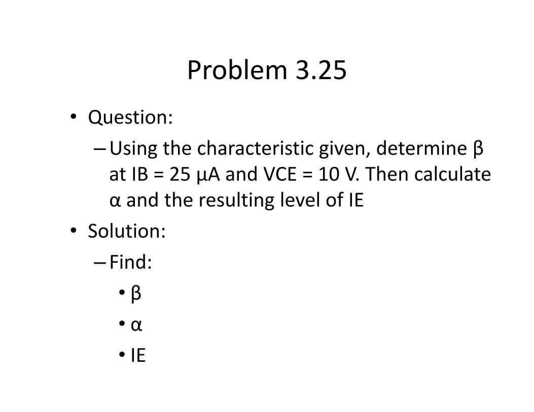
Problem 3.25Problem 3.25
• Question:
–Using the characteristic given, determine βat IB = 25 μA and VCE = 10 V. Then calculateat IB 25 μA and VCE 10 V. Then calculate α and the resulting level of IE
• Solution:• Solution:
– Find:
• β• α• IE

Problem 3.25Problem 3.25
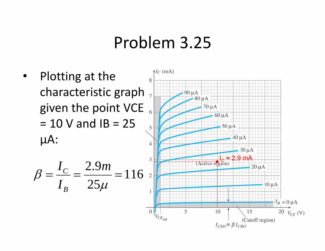
Problem 3.25Problem 3.25
• Plotting at thePlotting at the characteristic graph given the point VCEgiven the point VCE = 10 V and IB = 25 μA:μA:
IC ≈ 2.9 mA
1169.2β mIC 11625
===μ
βIB
C
Problem 3.25Problem 3.25
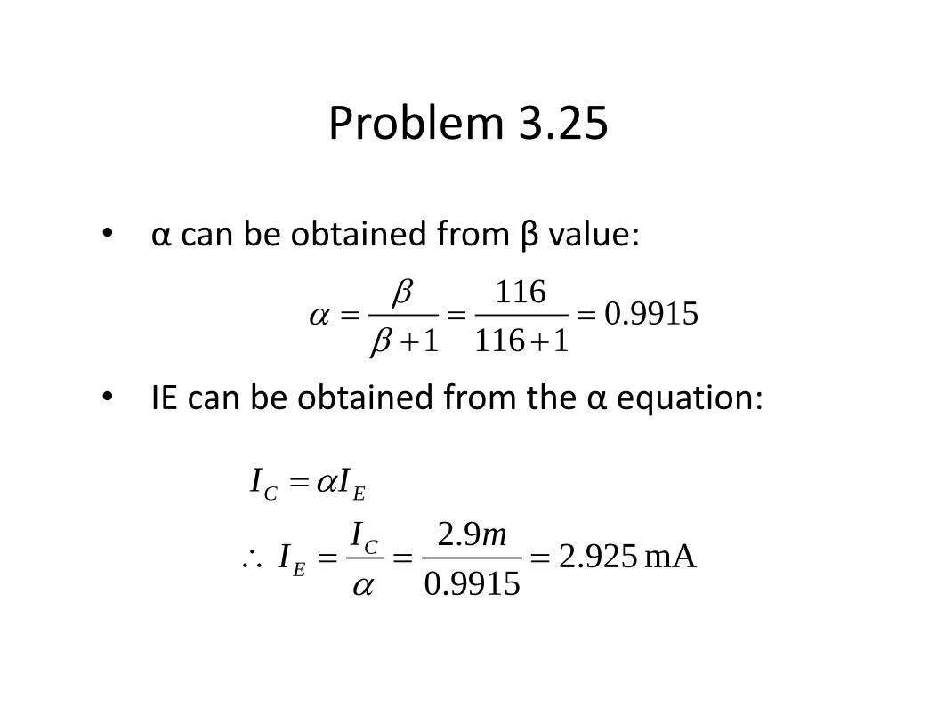
b bt i d f β l• α can be obtained from β value:
99150116===
βα
• IE can be obtained from the α equation:
9915.011161=
+=
+=β
α
IE can be obtained from the α equation:
= II EC α
mA 925.2991509.2
===∴mII C
E
EC
α 9915.0α
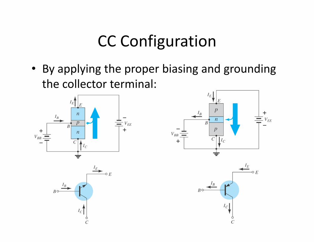
CC ConfigurationCC Configuration
• By applying the proper biasing and grounding the collector terminal:

CC ConfigurationCC Configuration• In CC configuration, the input terminal is between terminal B and C (due to ground atbetween terminal B and C (due to ground at C)
h l f d b l• The output terminal is fixed between terminal E and C
+ output+
−−VBC
VECinput
CC ConfigurationCC Configuration• By examining the input of CB and CE configuration notice that they are the sameconfiguration, notice that they are the same (VBE = 0.7 V). As for that the input for CC configuration remains the sameconfiguration remains the same
• For CE the output voltage is VCE while the output current is IC Meanwhile in CC theoutput current is IC. Meanwhile in CC, the output voltage is VEC and the output current is IE
• As for IC ≈ IE and VCE = VEC (polarity change only), it is said that the characteristic of CE y),and CC configuration are the same
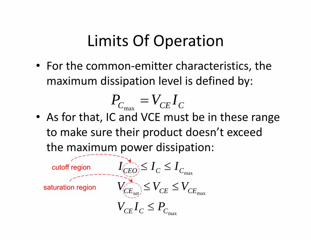
Limits Of OperationLimits Of Operation• For the common‐emitter characteristics, the maximum dissipation level is defined by:
CCEC IVP =• As for that, IC and VCE must be in these range to make sure their product doesn’t exceed
CCECmax
to make sure their product doesn t exceed the maximum power dissipation:
III ≤≤t ff i
max
max
CECECE
CCCEO
VVV
III
sat≤≤
≤≤cutoff region
saturation region
maxCCCE PIV ≤

Limits Of Operation• For example, if a transistor’s collector power dissipation is specified to 300 mW with ICmax = 50 p pmA and VCEmax = 20 V
• For ICmax value, VCE would be: mA 1520
300===
mV
PI CC,
• For VCEmax value, IC would be:
300mPC
20max
VCE
• Adding two more points to complete the curve:
V650300
max
===mm
IPVC
CCE
Adding two more points to complete the curve:
300mA 30=
mPI
C
C
300mA 25=
mPI
C
C
V1030300
===∴mm
IPV
C
CCE V12
25300
===∴mm
IPV
C
CCE

Limits Of OperationLimits Of Operation• Connects all the points obtained, the curve bbecomes:

Limits Of OperationLimits Of Operation
• The same goes for a common‐base configuration, its maximum power is defined as:
IVP• And the IC and VCE range is defined as:
CCBC IVP =max
• And the IC and VCE range is defined as:
maxCCCEO III ≤≤
max
a
CBCBCB VVVsat
≤≤
maxCCCB PIV ≤

Transistor DatasheetTransistor Datasheet
• Some of the important specification columnsSome of the important specification columns are bolded
VCE I PVCEmax ICmax PCmax

Transistor DatasheetTransistor Datasheet
ICBO (cutoff) for common-base ICEO (cutoff) for common-emitter
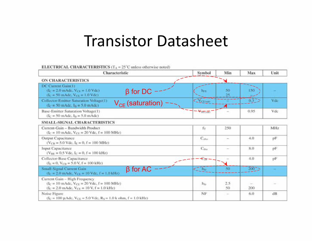
Transistor DatasheetTransistor Datasheet
β for DCVCE (saturation)CE (sa u a o )
β for AC