
EDPGA Chapter 3 - UPB · Embedded Design using Programmable Gate Arrays Chapter 3 Spartan-3E...
100
Chapter 3 Chapter 3 Programmable Gate Programmable Gate Array Hardware Array Hardware
-
Upload
nguyendang -
Category
Documents
-
view
239 -
download
0
Transcript of EDPGA Chapter 3 - UPB · Embedded Design using Programmable Gate Arrays Chapter 3 Spartan-3E...

Chapter 3Chapter 3
Programmable GateProgrammable GateArray HardwareArray Hardware

Embedded Design using Programmable Gate Arrays Chapter 3
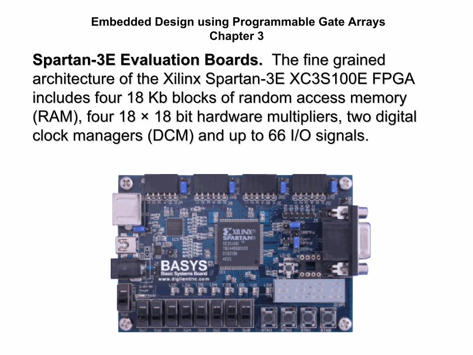
SpartanSpartan--3E Evaluation Boards. 3E Evaluation Boards. The Digilent Basys The Digilent Basys (Basic Systems) Board ((Basic Systems) Board (www.digilentinc.comwww.digilentinc.com) is an ) is an inexpensive Xilinx Spartaninexpensive Xilinx Spartan--3E FPGA development and 3E FPGA development and evaluation boards. The Xilinx Spartanevaluation boards. The Xilinx Spartan--3E XC3S100E3E XC3S100E--VQ100 FPGA on the evaluation board contains 100 K VQ100 FPGA on the evaluation board contains 100 K gates with the equivalent of 2160 logic cells.gates with the equivalent of 2160 logic cells.
Embedded Design using Programmable Gate Arrays Chapter 3
SpartanSpartan--3E Evaluation Boards. 3E Evaluation Boards. The fine grained The fine grained architecture of the Xilinx Spartanarchitecture of the Xilinx Spartan--3E XC3S100E FPGA 3E XC3S100E FPGA includes four 18 Kb blocks of random access memory includes four 18 Kb blocks of random access memory (RAM), four 18 (RAM), four 18 ×× 18 bit hardware multipliers, two digital 18 bit hardware multipliers, two digital clock managers (DCM) and up to 66 I/O signals.clock managers (DCM) and up to 66 I/O signals.

Embedded Design using Programmable Gate Arrays Chapter 3
SpartanSpartan--3E Evaluation Boards.3E Evaluation Boards. The SpartanThe Spartan--3E Starter 3E Starter Board is a more versatile but more expensive Board is a more versatile but more expensive development and evaluation board. The Xilinx Spartandevelopment and evaluation board. The Xilinx Spartan--3E 3E XC3S500EXC3S500E--FG320FG320FPGA on theFPGA on theevaluation boardevaluation boardcontains 500 K gatescontains 500 K gateswith the equivalent ofwith the equivalent of10 476 logic cells. 10 476 logic cells.

Embedded Design using Programmable Gate Arrays Chapter 3
SpartanSpartan--3E Evaluation Boards.3E Evaluation Boards. The fine grained The fine grained architecture of the Xilinx Spartanarchitecture of the Xilinx Spartan--3E XC3S500 FPGA 3E XC3S500 FPGA includes twenty 18 Kb blocks of RAM, twenty 18 includes twenty 18 Kb blocks of RAM, twenty 18 ×× 18 bit 18 bit hardware multipliers,hardware multipliers,four digital clockfour digital clockmanagers (DCM) andmanagers (DCM) andup to 232 I/O signals.up to 232 I/O signals.

Embedded Design using Programmable Gate Arrays Chapter 3
User Constraint File (UCF)User Constraint File (UCF). The UCF s3esb.ucf provides . The UCF s3esb.ucf provides the basic definitions for the hardthe basic definitions for the hard--wired peripherals and wired peripherals and accessories of the Spartanaccessories of the Spartan--3E Starter Board. The initial 3E Starter Board. The initial timing constrainttiming constraint on CCLK for the Spartanon CCLK for the Spartan--3E Starter 3E Starter Board can obviated by commenting or removing that line. Board can obviated by commenting or removing that line.
Listing 3.2 Listing 3.2 User Constraints File for the SpartanUser Constraints File for the Spartan--3E Starter Board s3esb.ucf3E Starter Board s3esb.ucf
# Xilinx Spartan# Xilinx Spartan--3E Starter Board 3E Starter Board # User Constraints File (UCF) s3esb.ucf# User Constraints File (UCF) s3esb.ucf
# Crystal Clock Oscillator# Crystal Clock Oscillator#NET#NET "CCLK""CCLK" LOC = "C9" LOC = "C9" | IOSTANDARD = LVCMOS33;| IOSTANDARD = LVCMOS33;#NET #NET "CCLK""CCLK" PERIOD = 20.0ns HIGH 40%;PERIOD = 20.0ns HIGH 40%;
[more][more]

Embedded Design using Programmable Gate Arrays Chapter 3
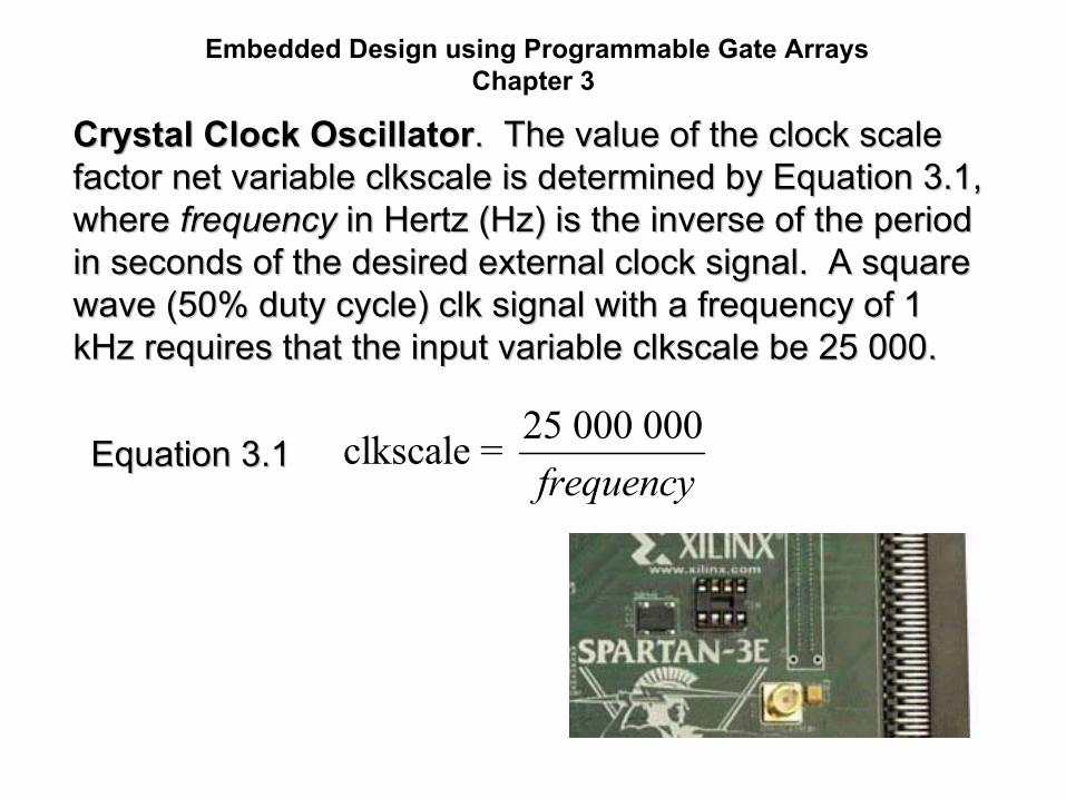
Crystal Clock OscillatorCrystal Clock Oscillator. The 50 MHz crystal clock . The 50 MHz crystal clock oscillator external peripheral on the Basys Board and the oscillator external peripheral on the Basys Board and the SpartanSpartan--3E Starter Board can function as the clock for 3E Starter Board can function as the clock for synchronous logic operation of the FPGA. The clock synchronous logic operation of the FPGA. The clock oscillator has a 40% to 60% duty cycle and an accuracy of oscillator has a 40% to 60% duty cycle and an accuracy of ±± 2500 Hz or 2500 Hz or ±± 50 parts per million (50 parts per million (ppmppm). ).
Crystal clock Crystal clock oscillatoroscillator

Embedded Design using Programmable Gate Arrays Chapter 3
Crystal Clock OscillatorCrystal Clock Oscillator. The minimum clock period of . The minimum clock period of 20 nanoseconds (nsec) is exceedingly fast for projects 20 nanoseconds (nsec) is exceedingly fast for projects that utilize the pushbuttons, slide switches, LEDs and the that utilize the pushbuttons, slide switches, LEDs and the LED sevenLED seven--segment display or LCD. segment display or LCD.
External clock External clock inputinput
Additional clock oscillator socketAdditional clock oscillator socket

Embedded Design using Programmable Gate Arrays Chapter 3
Crystal Clock OscillatorCrystal Clock Oscillator. The module . The module clock.vclock.v in Listing in Listing 3.2 3.2 increases the period by comparing the 50 MHz increases the period by comparing the 50 MHz master crystal clock input signal CCLK accumulated in the master crystal clock input signal CCLK accumulated in the register register clkqclkq to the input 32to the input 32--bit variable bit variable clkscaleclkscale to provide to provide an external an external clkclk signal that is used in the application.signal that is used in the application.
Listing 3.3Listing 3.3 Crystal clock oscillator module Crystal clock oscillator module clock.vclock.v
module clock (input CCLK, input [31:0] module clock (input CCLK, input [31:0] clkscaleclkscale, output reg , output reg clkclk););
// CCLK master crystal clock oscillator 50 MHz// CCLK master crystal clock oscillator 50 MHzreg [31:0] reg [31:0] clkqclkq = 0;= 0; // clock register, initial value of 0// clock register, initial value of 0

Embedded Design using Programmable Gate Arrays Chapter 3
Crystal Clock OscillatorCrystal Clock Oscillator. The 32. The 32--bit register bit register clkqclkq is is initialized to 0 here on global reset or powerinitialized to 0 here on global reset or power--up by a up by a declaration, although the default value on powerdeclaration, although the default value on power--up would up would also be 0.also be 0.
always@(posedgealways@(posedge CCLK)CCLK)beginbegin
clkqclkq = = clkqclkq + 1;+ 1; // increment clock register// increment clock registerif (if (clkqclkq >= >= clkscaleclkscale) ) // clock scaling// clock scaling
beginbeginclkclk = ~= ~clkclk; // output clock; // output clockclkqclkq = 0;= 0; // reset clock register// reset clock register
endendendend
endmoduleendmodule
Embedded Design using Programmable Gate Arrays Chapter 3
Crystal Clock OscillatorCrystal Clock Oscillator. The value of the clock scale . The value of the clock scale factor net variable factor net variable clkscaleclkscale is determined by Equation 3.1, is determined by Equation 3.1, where where frequencyfrequency in Hertz (Hz) is the inverse of the period in Hertz (Hz) is the inverse of the period in seconds of the desired external clock signal. A square in seconds of the desired external clock signal. A square wave (50% duty cycle) wave (50% duty cycle) clkclk signal with a frequency of 1 signal with a frequency of 1 kHz requires that the input variable kHz requires that the input variable clkscaleclkscale be 25 000.be 25 000.
25 000 000clkscale = frequency
Equation 3.1Equation 3.1
Embedded Design using Programmable Gate Arrays Chapter 3
Crystal Clock OscillatorCrystal Clock Oscillator.. The clock oscillator module The clock oscillator module clock.vclock.v is verified by the Verilog top module is verified by the Verilog top module clocktest.vclocktest.v. . The LEDs are simply mapped in The LEDs are simply mapped in clocktest.vclocktest.v module to the module to the only output of each instance of the only output of each instance of the clock.vclock.v module and module and blink at rates of 1, 2, and 4 Hz.blink at rates of 1, 2, and 4 Hz.
Listing 3.4Listing 3.4 Clock oscillator test top module Clock oscillator test top module clocktest.vclocktest.v
module module clocktestclocktest (input CCLK, output LD0, LD1, LD2);(input CCLK, output LD0, LD1, LD2);
clock M0 (CCLK, 25000000, LD0);clock M0 (CCLK, 25000000, LD0); // 1 Hz clock// 1 Hz clockclock M1 (CCLK, 12500000, LD1);clock M1 (CCLK, 12500000, LD1); // 2 Hz clock// 2 Hz clockclock M2 (CCLK, 6250000, LD2);clock M2 (CCLK, 6250000, LD2); // 4 Hz clock// 4 Hz clock
endmoduleendmodule

Embedded Design using Programmable Gate Arrays Chapter 3
Light Emitting Diodes. Light Emitting Diodes. The LED hardThe LED hard--wired accessory wired accessory on the Spartanon the Spartan--3E Starter Board can function as an 3E Starter Board can function as an indicator in embedded applications of the FPGA.indicator in embedded applications of the FPGA.
The module The module bargraph.vbargraph.v utilizes all eight available LEDs utilizes all eight available LEDs and provides a bar graph display useful for peak and provides a bar graph display useful for peak amplitudeamplitudemeasurements inmeasurements inaudio andaudio andcommunicationscommunicationssignal processing.signal processing.

Embedded Design using Programmable Gate Arrays Chapter 3
Light Emitting Diodes.Light Emitting Diodes. The module demonstrates the The module demonstrates the simple mapping as a continuous assignment of an LED to simple mapping as a continuous assignment of an LED to a logic signal [Ciletti99]. The module is event driven on a logic signal [Ciletti99]. The module is event driven on the positive edge of the input signal the positive edge of the input signal clkclk and uses the and uses the largest nonlargest non--zero bit of the 8zero bit of the 8--bit input data to produce a bar bit input data to produce a bar graph display. In Listing 3.4 the 1graph display. In Listing 3.4 the 1--bit clock register could bit clock register could be mapped directly tobe mapped directly toa single LED. Thea single LED. Theeight continuouseight continuousassignment Verilogassignment Verilogstatement assignstatement assignperforms the requisiteperforms the requisite88--bit register mapping. bit register mapping.

Embedded Design using Programmable Gate Arrays Chapter 3
Light Emitting Diodes.Light Emitting Diodes.
Listing 3.5Listing 3.5 LED bar graph module LED bar graph module bargraph.vbargraph.v
module module bargraphbargraph (input (input clkclk, input [7:0] data, output LD7, LD6, LD5, LD4, LD3, , input [7:0] data, output LD7, LD6, LD5, LD4, LD3, LD2, LD1, LD0);LD2, LD1, LD0);
reg [7:0] reg [7:0] leddataleddata;; // LED data// LED data
assign LD7 = leddata[7];assign LD7 = leddata[7]; // continuous assignment// continuous assignmentassign LD6 = leddata[6];assign LD6 = leddata[6]; // for LED data output// for LED data outputassign LD5 = leddata[5];assign LD5 = leddata[5];assign LD4 = leddata[4];assign LD4 = leddata[4];assign LD3 = leddata[3];assign LD3 = leddata[3];assign LD2 = leddata[2];assign LD2 = leddata[2];assign LD1 = leddata[1];assign LD1 = leddata[1];assign LD0 = leddata[0];assign LD0 = leddata[0];

Embedded Design using Programmable Gate Arrays Chapter 3
Light Emitting Diodes.Light Emitting Diodes.
always@(posedgealways@(posedge clkclk)) // local clock event driven// local clock event drivenbeginbegin
leddataleddata = 8'b00000000;= 8'b00000000; // bar graph pattern based// bar graph pattern basedif (data[0] == 1)if (data[0] == 1) // based on the least// based on the least
leddataleddata = 8'b00000001;= 8'b00000001; // bit set to logic 1// bit set to logic 1if (data[1] == 1)if (data[1] == 1)
leddataleddata = 8'b00000011;= 8'b00000011;if (data[2] == 1)if (data[2] == 1)
leddata = 8'b00000111;leddata = 8'b00000111;if (data[3] == 1)if (data[3] == 1)
leddata=8'b00001111;leddata=8'b00001111;[more][more]
if (data[7] == 1)if (data[7] == 1)leddataleddata=8'b11111111;=8'b11111111;
endend
endmoduleendmodule

Embedded Design using Programmable Gate Arrays Chapter 3
Light Emitting Diodes. Light Emitting Diodes. The bar graph module The bar graph module bargraph.vbargraph.v is verified by the Verilog top module is verified by the Verilog top module bargraphtest.vbargraphtest.v. The data is generated as a simple ramp . The data is generated as a simple ramp by the stimulus module by the stimulus module gendata.vgendata.v on the negative edge of on the negative edge of the clock input signal. The wire net type establishes the the clock input signal. The wire net type establishes the 88--bit vector connectivity for data between the bit vector connectivity for data between the bargraph.vbargraph.vand and gendata.vgendata.v modules.modules.The clock signal The clock signal clkclk isisoutputted from theoutputted from theclock.vclock.v module andmodule andinputted to both theinputted to both thebargraph.vbargraph.v andandgendata.vgendata.v modules.modules.

Embedded Design using Programmable Gate Arrays Chapter 3
Light Emitting Diodes. Light Emitting Diodes. In Listing 3.6 the statement In Listing 3.6 the statement output reg [7:0] output reg [7:0] gdatagdata defines and maps the generated defines and maps the generated data as an 8data as an 8--bit register to the output vector net for use by bit register to the output vector net for use by other Verilog modules. Note that the name of the other Verilog modules. Note that the name of the generated signal data in the top module generated signal data in the top module bargraphtest.vbargraphtest.v(data) does not have to agree with the name of the (data) does not have to agree with the name of the generated register datagenerated register datain the in the gendata.vgendata.vmodule (module (gdatagdata) since) sincethe connection bythe connection byposition option for theposition option for theports of a module isports of a module isused here.used here.

Embedded Design using Programmable Gate Arrays Chapter 3
Light Emitting DiodesLight Emitting Diodes..
Listing 3.6Listing 3.6 LED bar graph test top module LED bar graph test top module bargraphtest.vbargraphtest.v
module module bargraphtestbargraphtest (input CCLK, output LD7, LD6, LD5, LD4, LD3, LD2, (input CCLK, output LD7, LD6, LD5, LD4, LD3, LD2, LD1, LD0);LD1, LD0);
wire [7:0] data;wire [7:0] data;
clock M0 (CCLK, 250000, clock M0 (CCLK, 250000, clkclk);); // 100 Hz clock // 100 Hz clock bargraphbargraph M1 (M1 (clkclk, data, LD7, LD6, LD5, LD4, LD3, LD2, LD1, LD0); , data, LD7, LD6, LD5, LD4, LD3, LD2, LD1, LD0); gendatagendata M2 (M2 (clkclk, data);, data);
endmoduleendmodule

Embedded Design using Programmable Gate Arrays Chapter 3
Light Emitting DiodesLight Emitting Diodes..
module module gendatagendata (input clock, output reg [7:0] (input clock, output reg [7:0] gdatagdata); ); // generate bar graph // generate bar graph // test data// test data
always@(negedgealways@(negedge clock)clock) // local clock event driven// local clock event drivengdatagdata = = gdatagdata + 1;+ 1; // increment generated data// increment generated data
endmoduleendmodule

Embedded Design using Programmable Gate Arrays Chapter 3
Push ButtonsPush Buttons. The push buttons are often used for . The push buttons are often used for counting functions in FPGA applications where contact counting functions in FPGA applications where contact bouncebounce can cause an aberrant result. The top module can cause an aberrant result. The top module pbdebouncetest.vpbdebouncetest.v illustrates the use of a serial shift illustrates the use of a serial shift register to insure that if a contact bounce occurs then only register to insure that if a contact bounce occurs then only a single output pulse results.a single output pulse results.
The module The module pbdebounce.vpbdebounce.v isisutilized within the top moduleutilized within the top modulepbdebouncetest.vpbdebouncetest.v. .

Embedded Design using Programmable Gate Arrays Chapter 3
Push ButtonsPush Buttons. A 4. A 4--bit register bit register pbshiftpbshift is logically (no is logically (no wrapwrap--around) left shifted on the positive edge of a 10 Hz around) left shifted on the positive edge of a 10 Hz clock provided by the clock provided by the clock.vclock.v module. The least module. The least significant bit of the shift register is set equal to the push significant bit of the shift register is set equal to the push button (BTN0). If all four bits of button (BTN0). If all four bits of pbshiftpbshift contain logic 1 contain logic 1 (1111 or 15 decimal), then the push button register output (1111 or 15 decimal), then the push button register output pbregpbreg is set to logic 1. If all four bits contain logic 0, then is set to logic 1. If all four bits contain logic 0, then the push button registerthe push button registeroutput output pbregpbreg is set to logic 0.is set to logic 0.
Any other 4Any other 4--bit patternbit patternindicates that a push buttonindicates that a push buttonbounce has occurred andbounce has occurred andpbregpbreg is unchanged.is unchanged.

Embedded Design using Programmable Gate Arrays Chapter 3
Push ButtonsPush Buttons..
Listing 3.8Listing 3.8 Push button contact debounce test top module Push button contact debounce test top module pbdebouncetest.vpbdebouncetest.v
module module pbdebouncetestpbdebouncetest (input CCLK, input BTN0,output LD7, LD6, LD5, (input CCLK, input BTN0,output LD7, LD6, LD5, LD4, LD3, LD2, LD1, LD0);LD4, LD3, LD2, LD1, LD0);
wire [3:0] wire [3:0] leddataleddata;;wire [3:0] wire [3:0] dataleddataled;;
assign LD7 = dataled[3];assign LD7 = dataled[3]; // continuous assignment// continuous assignmentassign LD6 = dataled[2];assign LD6 = dataled[2]; // for LED data output// for LED data outputassign LD5 = dataled[1];assign LD5 = dataled[1];assign LD4 = dataled[0];assign LD4 = dataled[0];assign LD3 = leddata[3];assign LD3 = leddata[3];assign LD2 = leddata[2];assign LD2 = leddata[2];assign LD1 = leddata[1];assign LD1 = leddata[1];assign LD0 = leddata[0];assign LD0 = leddata[0];

Embedded Design using Programmable Gate Arrays Chapter 3
Push ButtonsPush Buttons..
clock M0 (CCLK, 2500000, clock M0 (CCLK, 2500000, clkclk);); // 10 Hz clock// 10 Hz clockpbdebouncepbdebounce M1 (M1 (clkclk, BTN0, , BTN0, pbregpbreg););ledtest M2 (pbreg, BTN0, leddata, dataled);ledtest M2 (pbreg, BTN0, leddata, dataled);endmoduleendmodule
module module ledtestledtest (input (input pbregpbreg, input button, output reg [3:0] , input button, output reg [3:0] leddataleddata,,output reg [3:0] output reg [3:0] dataleddataled););
always@(posedgealways@(posedge pbregpbreg)) // debounced pushbutton event driven // debounced pushbutton event driven beginbegin
leddataleddata = = leddataleddata + 1;+ 1; // increment counter// increment counterendend
always@(posedgealways@(posedge button)button) // chattering pushbutton event driven// chattering pushbutton event drivenbeginbegin
dataleddataled = = dataleddataled + 1;+ 1; // increment counter// increment counterendend
endmoduleendmodule

Embedded Design using Programmable Gate ArraysChapter 3
Push ButtonsPush Buttons..
Listing 3.9Listing 3.9 Push button debounce Push button debounce pbdebounce.vpbdebounce.v
module module pbdebouncepbdebounce (input (input clkclk, input button, output reg , input button, output reg pbregpbreg););
reg [3:0] reg [3:0] pbshiftpbshift;;
always@(posedgealways@(posedge clkclk)) // local clock event driven// local clock event drivenbeginbegin
pbshiftpbshift = = pbshiftpbshift << 1;<< 1; // shift register// shift registerpbshift[0] = button;pbshift[0] = button; // read button// read button
if (if (pbshiftpbshift == 0)== 0) // if a bounce occurs// if a bounce occurspbregpbreg = 0;= 0; // clear the register// clear the register
if (if (pbshiftpbshift == 15)== 15) // 15 local clock tics without a bounce// 15 local clock tics without a bouncepbregpbreg = 1;= 1; // sets the register// sets the register
endend
endmoduleendmodule

Embedded Design using Programmable Gate ArraysChapter 3
Rotary Shaft EncoderRotary Shaft Encoder. The hard. The hard--wired accessory rotary wired accessory rotary shaft encoder on the Spartanshaft encoder on the Spartan--3E Starter Board functions 3E Starter Board functions as asynchronous input signals in applications of the as asynchronous input signals in applications of the FPGA.FPGA.
Depressing the center shaft provides an additional push Depressing the center shaft provides an additional push button switch which generates logic 1 on the ROTCTR button switch which generates logic 1 on the ROTCTR signal. Rotating the shaftsignal. Rotating the shaftclockwise provides a logic 1clockwise provides a logic 1on the ROTA signal before aon the ROTA signal before alogic 1 appears on the ROTBlogic 1 appears on the ROTBsignal.signal.

Embedded Design using Programmable Gate ArraysChapter 3
Rotary Shaft EncoderRotary Shaft Encoder. Rotating the shaft counter . Rotating the shaft counter --clockwise provides a logic 1 on the ROTB signal before aclockwise provides a logic 1 on the ROTB signal before alogic 1 appears on the ROTA signal.logic 1 appears on the ROTA signal. When the shaft is When the shaft is stationary at the detent position both ROTA and ROTB stationary at the detent position both ROTA and ROTB are logic 0.are logic 0.
The rotary shaft encoder signals ROTA, ROTB and The rotary shaft encoder signals ROTA, ROTB and ROTCTR have no activeROTCTR have no activedebouncing circuitry and aredebouncing circuitry and aredefined in the UCF of thedefined in the UCF of theSpartanSpartan--3E Starter Board. 3E Starter Board.

Embedded Design using Programmable Gate ArraysChapter 3
Rotary Shaft EncoderRotary Shaft Encoder. Each of the rotary shaft encoder . Each of the rotary shaft encoder signals are debounced by the same process described in signals are debounced by the same process described in the module the module pbdebounce.vpbdebounce.v. The debounced shaft encoder . The debounced shaft encoder signals here are the register variables signals here are the register variables rotAregrotAreg, , rotBregrotBregand and rotCTRregrotCTRreg..

Embedded Design using Programmable Gate ArraysChapter 3
Rotary Shaft EncoderRotary Shaft Encoder..
Listing 3.10Listing 3.10 Rotary shaft encoder module Rotary shaft encoder module rotary.vrotary.v
module rotary (input module rotary (input clkclk, ROTA, ROTB, ROTCTR, output reg , ROTA, ROTB, ROTCTR, output reg rotAregrotAreg,,output reg output reg rotBregrotBreg, output reg , output reg rotCTRregrotCTRreg););
reg [3:0] reg [3:0] rotAshiftrotAshift;;reg [3:0] reg [3:0] rotBshiftrotBshift;;reg [3:0] reg [3:0] rotCTRshiftrotCTRshift;;
always@(posedgealways@(posedge clkclk)) // local clock event driven// local clock event drivenbeginbegin
rotCTRshiftrotCTRshift = = rotCTRshiftrotCTRshift << 1; // debounce for ROTCTR<< 1; // debounce for ROTCTRrotCTRshift[0] = ROTCTR;rotCTRshift[0] = ROTCTR;if (if (rotCTRshiftrotCTRshift == 0)== 0)
rotCTRregrotCTRreg = 0;= 0;if (if (rotCTRshiftrotCTRshift == 15)== 15)
rotCTRregrotCTRreg = 1;= 1;

Embedded Design using Programmable Gate ArraysChapter 3
Rotary Shaft EncoderRotary Shaft Encoder..
rotAshiftrotAshift = = rotAshiftrotAshift << 1;<< 1; // debounce for ROTA// debounce for ROTArotAshift[0] = ROTA;rotAshift[0] = ROTA;if (if (rotAshiftrotAshift == 15)== 15)
rotAregrotAreg = 0;= 0;if (if (rotAshiftrotAshift == 0)== 0)
rotAregrotAreg = 1;= 1;
rotBshiftrotBshift = = rotBshiftrotBshift << 1; // debounce for ROTB<< 1; // debounce for ROTBrotBshift[0] = ROTB;rotBshift[0] = ROTB;if (if (rotBshiftrotBshift == 15)== 15)
rotBregrotBreg = 0;= 0;if (if (rotBshiftrotBshift == 0)== 0)
rotBregrotBreg = 1;= 1;endend
endmoduleendmodule

Embedded Design using Programmable Gate ArraysChapter 3
Rotary Shaft EncoderRotary Shaft Encoder. The wire net type establishes the . The wire net type establishes the 44--bit vector connectivity for bit vector connectivity for leddataleddata and and dataleddataled between between the the ledtest.vledtest.v and and rotarytest.vrotarytest.v modules.modules.
The LED external signals LD7 through LD4 and LD7 The LED external signals LD7 through LD4 and LD7 through LD4 are assigned to register dataled[3]through through LD4 are assigned to register dataled[3]through dataled[0] and leddata[3]through leddata[0], respectively, dataled[0] and leddata[3]through leddata[0], respectively, since they are only referencedsince they are only referencedin the top module in the top module rotarytest.vrotarytest.v..

Embedded Design using Programmable Gate ArraysChapter 3
Rotary Shaft EncoderRotary Shaft Encoder. The module . The module ledtest.vledtest.v loads the loads the rightmost four LEDs of the Spartanrightmost four LEDs of the Spartan--3E Starter Board with 3E Starter Board with the 4the 4--bit register bit register leddataleddata which increments or decrements which increments or decrements on the logic of the debounced register variable on the logic of the debounced register variable rotBregrotBreg on on the positive edge of the debounced register variable the positive edge of the debounced register variable rotAregrotAreg..
The leftmost four LEDs areThe leftmost four LEDs areloaded with the 4loaded with the 4--bit registerbit registerdataleddataled which increments orwhich increments ordecrements on the logic of thedecrements on the logic of thechattering register variablechattering register variableROTB on the positive edge ofROTB on the positive edge ofthe chattering register variablethe chattering register variableROTA.ROTA.

Embedded Design using Programmable Gate ArraysChapter 3
Rotary Shaft EncoderRotary Shaft Encoder. A clockwise rotation of the rotary . A clockwise rotation of the rotary shaft encoder increments the register, while a shaft encoder increments the register, while a counterclockwise rotation decrements the register.counterclockwise rotation decrements the register.
These registers are cleared with the debounced register These registers are cleared with the debounced register variable variable rotCTRregrotCTRreg or the chattering register variable or the chattering register variable ROTCTR which results from the depression of the shaft of ROTCTR which results from the depression of the shaft of the rotary encoder.the rotary encoder.

Embedded Design using Programmable Gate ArraysChapter 3
Rotary Shaft EncoderRotary Shaft Encoder..
Listing 3.11Listing 3.11 Rotary shaft encoder top module Rotary shaft encoder top module rotarytest.vrotarytest.v
module module rotarytestrotarytest (input CCLK, ROTA, ROTB, ROTCTR, output LD7, LD6, (input CCLK, ROTA, ROTB, ROTCTR, output LD7, LD6, LD5, LD4, LD3, LD2, LD1, LD0);LD5, LD4, LD3, LD2, LD1, LD0);
wire wire rotAregrotAreg;;wire wire rotBregrotBreg;;wire [3:0] wire [3:0] leddataleddata;;wire [3:0] wire [3:0] dataleddataled;;
assign LD7 = dataled[3];assign LD7 = dataled[3];assign LD6 = dataled[2];assign LD6 = dataled[2];assign LD5 = dataled[1];assign LD5 = dataled[1];assign LD4 = dataled[0];assign LD4 = dataled[0];assign LD3 = leddata[3];assign LD3 = leddata[3];assign LD2 = leddata[2];assign LD2 = leddata[2];assign LD1 = leddata[1];assign LD1 = leddata[1];assign LD0 = leddata[0];assign LD0 = leddata[0];
Embedded Design using Programmable Gate ArraysChapter 3
Rotary Shaft EncoderRotary Shaft Encoder..
clock M0 (CCLK, 25000, clock M0 (CCLK, 25000, clkclk);); // 1 kHz clock// 1 kHz clockrotary M1 (rotary M1 (clkclk, ROTA, ROTB, ROTCTR, , ROTA, ROTB, ROTCTR, rotAregrotAreg, , rotBregrotBreg, , rotCTRregrotCTRreg););ledtestledtest M2 (ROTA, ROTB, M2 (ROTA, ROTB, rotAregrotAreg, , rotBregrotBreg, ROTCTR, , ROTCTR, rotCTRregrotCTRreg, , leddataleddata, ,
dataleddataled););endmoduleendmodule
module module ledtestledtest (input ROTA, ROTB, (input ROTA, ROTB, rotAregrotAreg, , rotBregrotBreg, ROTCTR, , ROTCTR, rotCTRregrotCTRreg,,output reg [3:0] output reg [3:0] leddataleddata, output reg [3:0] , output reg [3:0] dataleddataled););
always@(posedgealways@(posedge rotAregrotAreg)) // event driven on debounced// event driven on debouncedbeginbegin // shaft encoder ROTA// shaft encoder ROTA
if (if (rotBregrotBreg == 0 && == 0 && rotCTRregrotCTRreg == 0)== 0)leddata = leddata + 1;leddata = leddata + 1;
elseelseleddata = leddata leddata = leddata –– 1;1;
if (if (rotCTRregrotCTRreg == 1)== 1)leddataleddata = 0;= 0;
endend

Embedded Design using Programmable Gate ArraysChapter 3
Rotary Shaft EncoderRotary Shaft Encoder..
always@(posedgealways@(posedge ROTA)ROTA) // even driven on chattering// even driven on chatteringbeginbegin // shaft encoder ROTA// shaft encoder ROTA
if (ROTB == 0 && if (ROTB == 0 && rotctrrotctr == 0)== 0)dataleddataled = = dataleddataled + 1;+ 1;
elseelsedataleddataled = = dataleddataled –– 1;1;
if (ROTCTR == 1)if (ROTCTR == 1)dataleddataled = 0;= 0;
endend
endmoduleendmodule

Embedded Design using Programmable Gate ArraysChapter 3
Liquid Crystal DisplayLiquid Crystal Display. The hard. The hard--wired accessory liquid wired accessory liquid crystal display (LCD) on the Spartancrystal display (LCD) on the Spartan--3E Starter Board 3E Starter Board functions as an alphanumeric annunciator in applications functions as an alphanumeric annunciator in applications of the FPGA. The LCD features a 2of the FPGA. The LCD features a 2--line by 16line by 16--character. character. Updating the LCD at even a 0.5 second interval produces Updating the LCD at even a 0.5 second interval produces diminished clarity.diminished clarity.
Although a standard LCD can support an 8Although a standard LCD can support an 8--bit parallel bit parallel data interface, the Spartandata interface, the Spartan--3E Starter Board utilizes an 3E Starter Board utilizes an alternative 4alternative 4--bit parallelbit parallelinterface to minimize theinterface to minimize thetotal input/output (I/O)total input/output (I/O)pin count.pin count.
Embedded Design using Programmable Gate ArraysChapter 3
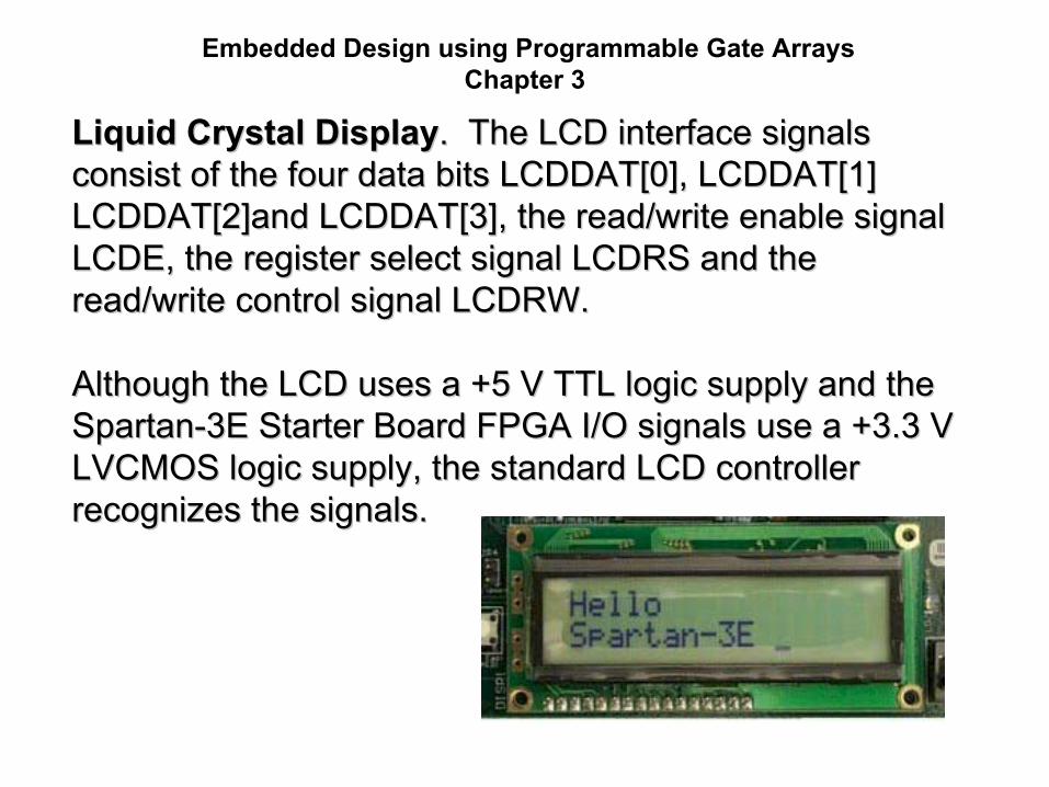
Liquid Crystal DisplayLiquid Crystal Display. The LCD interface signals . The LCD interface signals consist of the four data bits LCDDAT[0], LCDDAT[1] consist of the four data bits LCDDAT[0], LCDDAT[1] LCDDAT[2]and LCDDAT[3], the read/write enable signal LCDDAT[2]and LCDDAT[3], the read/write enable signal LCDE, the register select signal LCDRS and the LCDE, the register select signal LCDRS and the read/write control signal LCDRW.read/write control signal LCDRW.
Although the LCD uses a +5 V TTL logic supply and the Although the LCD uses a +5 V TTL logic supply and the SpartanSpartan--3E Starter Board FPGA I/O signals use a +3.3 V 3E Starter Board FPGA I/O signals use a +3.3 V LVCMOS logic supply, the standard LCD controller LVCMOS logic supply, the standard LCD controller recognizes the signals.recognizes the signals.

Embedded Design using Programmable Gate ArraysChapter 3
Liquid Crystal DisplayLiquid Crystal Display. The four data bits are shared . The four data bits are shared with the Intel 128 Mb with the Intel 128 Mb StrataFlashStrataFlash 28F256 PROM on the 28F256 PROM on the SpartanSpartan--3E Starter Board. However, for these applications 3E Starter Board. However, for these applications of the LCD in embedded system design the read/write of the LCD in embedded system design the read/write control signal LCDRW is set to logic 0 which provides control signal LCDRW is set to logic 0 which provides write access only to the LCD but full read/write access to write access only to the LCD but full read/write access to the PROM.the PROM.

Embedded Design using Programmable Gate ArraysChapter 3
Liquid Crystal DisplayLiquid Crystal Display. The standard LCD has three . The standard LCD has three internal memory regions. The display data (DD) RAM internal memory regions. The display data (DD) RAM stores the reference to a specific character bitmap to be stores the reference to a specific character bitmap to be displayed on the screen. The character bitmaps are displayed on the screen. The character bitmaps are stored in either the character generator (CG) ROM region stored in either the character generator (CG) ROM region or the useror the user--defined CG RAM region.defined CG RAM region.
For these applications ofFor these applications ofthe LCD in embeddedthe LCD in embeddedsystem design the CGsystem design the CGROM is used to provideROM is used to providethe fixed font bitmapsthe fixed font bitmapsreferenced by theirreferenced by theirASCII character code. ASCII character code.

Embedded Design using Programmable Gate ArraysChapter 3
Liquid Crystal DisplayLiquid Crystal Display. .
Table 3.1Table 3.1 Hexadecimal DD RAM addresses forHexadecimal DD RAM addresses for the 2the 2--line by 16line by 16--character character LCDLCD
PositionPosition 11 22 33 44 55 66 77 88
Line 1Line 1 0000 0101 0202 0303 0404 0505 0606 0707Line 2Line 2 4040 4141 4242 4343 4444 4545 4646 4747

Embedded Design using Programmable Gate ArraysChapter 3
Liquid Crystal DisplayLiquid Crystal Display. .
Table 3.1Table 3.1 Hexadecimal DD RAM addresses forHexadecimal DD RAM addresses for the 2the 2--line by 16line by 16--character character LCDLCD
PositionPosition 99 1010 1111 1212 1313 1414 1515 1616
Line 1Line 1 0808 0909 0A0A 0B0B 0C0C 0D0D 0E0E 0F0FLine 2Line 2 4848 4949 4A4A 4B4B 4C4C 4D4D 4E4E 4F4F

Embedded Design using Programmable Gate ArraysChapter 3
Liquid Crystal DisplayLiquid Crystal Display. The LCD 8. The LCD 8--bit command is sent bit command is sent as two 4as two 4--bit nibbles with the most significant 4bit nibbles with the most significant 4--bit nibble bit nibble transferred first. The entry X indicates a dontransferred first. The entry X indicates a don’’t care t care condition.condition.
The LCD read/write enable signal LCDE must be logic 1 The LCD read/write enable signal LCDE must be logic 1 for the commands to be effective. The LCD register select for the commands to be effective. The LCD register select signal LCDRS and the read/write control signal LCDRW signal LCDRS and the read/write control signal LCDRW are set, as listed in Table 3.2.are set, as listed in Table 3.2.

Embedded Design using Programmable Gate ArraysChapter 3
Liquid Crystal DisplayLiquid Crystal Display..
Table 3.2Table 3.2 CommonCommon LCD commandLCD command setset
CommandCommand LCDRSLCDRS LCDRW Upper Nibble Lower NibbleLCDRW Upper Nibble Lower Nibble
Clear DisplayClear Display 00 00 0 0 0 00 0 0 0 0 0 0 10 0 0 1Cursor HomeCursor Home 00 00 0 0 0 00 0 0 0 0 0 1 X0 0 1 XEntry ModeEntry Mode 00 0 0 0 0 0 00 0 0 0 0 1 I/D S0 1 I/D SDisplay On/OffDisplay On/Off 00 00 0 0 0 00 0 0 0 1 D C B1 D C BShift ModeShift Mode 00 00 0 0 0 10 0 0 1 S/C R/L X XS/C R/L X XFunction SetFunction Set 00 00 0 0 1 00 0 1 0 1 0 X X1 0 X XSet DD RAMSet DD RAM 00 00 1 A6 A5 A4 1 A6 A5 A4 A3 A2 A1 A0A3 A2 A1 A0
AddressAddressRead Busy FlagRead Busy Flag 00 11 BF A6 A5 A4 BF A6 A5 A4 A3 A2 A1 A0A3 A2 A1 A0Write Data toWrite Data to 11 0 0 D7 D6 D5 D4 D7 D6 D5 D4 D3 D2 D1 D0D3 D2 D1 D0
DD RAMDD RAM

Embedded Design using Programmable Gate ArraysChapter 3
Liquid Crystal DisplayLiquid Crystal Display. The entry mode command uses . The entry mode command uses the increment/decrement (I/D) bit to autothe increment/decrement (I/D) bit to auto--decrement with decrement with logic 0 or autologic 0 or auto--increment with logic 1 the address counter. increment with logic 1 the address counter. This appears as though the invisible or blinking cursor is This appears as though the invisible or blinking cursor is moving either left or right. moving either left or right.
Entry ModeEntry Mode 00 0 0 0 0 0 00 0 0 0 0 1 I/D S0 1 I/D S

Embedded Design using Programmable Gate ArraysChapter 3
Liquid Crystal DisplayLiquid Crystal Display. The clear display command . The clear display command writes a space or ASCII character code 20 hexadecimal writes a space or ASCII character code 20 hexadecimal (h) into all DD RAM locations, clears all the option settings (h) into all DD RAM locations, clears all the option settings and sets the I/D bit to logic 1 and the DD RAM address and sets the I/D bit to logic 1 and the DD RAM address counter to 00h or the topcounter to 00h or the top--left corner of the LCDleft corner of the LCD..
Clear DisplayClear Display 00 00 0 0 0 00 0 0 0 0 0 0 10 0 0 1

Embedded Design using Programmable Gate ArraysChapter 3
Liquid Crystal DisplayLiquid Crystal Display. The cursor home command only . The cursor home command only sets the DD RAM address counter to 00h without clearing sets the DD RAM address counter to 00h without clearing the LCD. the LCD.
Cursor HomeCursor Home 00 00 0 0 0 00 0 0 0 0 0 1 X0 0 1 X
Embedded Design using Programmable Gate ArraysChapter 3
Liquid Crystal DisplayLiquid Crystal Display. The shift mode command uses . The shift mode command uses the shift/cursor (S/C) bit and right/left (R/L) bit to provide the shift/cursor (S/C) bit and right/left (R/L) bit to provide four functions which shift the cursor or the entire display four functions which shift the cursor or the entire display without affecting the DD RAM contents. If these diwithout affecting the DD RAM contents. If these di--bits are bits are 00 the cursor shifts to the left and the DD RAM address 00 the cursor shifts to the left and the DD RAM address counter is decremented by one.counter is decremented by one.
Shift Mode 0Shift Mode 0 00 0 0 0 10 0 0 1 S/C R/L X XS/C R/L X X

Embedded Design using Programmable Gate ArraysChapter 3
Liquid Crystal DisplayLiquid Crystal Display. If these di. If these di--bits of the shift mode bits of the shift mode command are 01 the cursor shifts to the left and the DD command are 01 the cursor shifts to the left and the DD RAM address counter is incremented by one. If these diRAM address counter is incremented by one. If these di--bits are 10 the entire display and cursor shifts to the left bits are 10 the entire display and cursor shifts to the left and the DD RAM address counter is unchanged. If these and the DD RAM address counter is unchanged. If these didi--bits are 11 the entire display and cursor shift to the right bits are 11 the entire display and cursor shift to the right and the DD RAM address counter is unchanged.and the DD RAM address counter is unchanged.
Shift Mode 0Shift Mode 0 00 0 0 0 10 0 0 1 S/C R/L X XS/C R/L X X

Embedded Design using Programmable Gate ArraysChapter 3
Liquid Crystal DisplayLiquid Crystal Display. The function set command sets . The function set command sets the LCD interface data length, number of display lines and the LCD interface data length, number of display lines and character font. The Spartancharacter font. The Spartan--3E Starter Board LCD 3E Starter Board LCD supports only a single function code of 28h.supports only a single function code of 28h.
Function SetFunction Set 00 00 0 0 1 00 0 1 0 1 0 X X1 0 X X

Embedded Design using Programmable Gate ArraysChapter 3
Liquid Crystal DisplayLiquid Crystal Display. The set DD RAM address . The set DD RAM address command sets the initial value in the address counter and command sets the initial value in the address counter and subsequent LCD interface commands are executed with subsequent LCD interface commands are executed with the DD RAM.the DD RAM.
Set DD RAMSet DD RAM 00 00 1 A6 A5 A41 A6 A5 A4 A3 A2 A1 A0A3 A2 A1 A0AddressAddress
Embedded Design using Programmable Gate ArraysChapter 3
Liquid Crystal DisplayLiquid Crystal Display. The read busy flag/address . The read busy flag/address command reads the busy flag (BF) bit can be used to command reads the busy flag (BF) bit can be used to determine if an internal LCD interface operation is in determine if an internal LCD interface operation is in progress or returns the current DD RAM address if the set progress or returns the current DD RAM address if the set DD RAM address command was executed first.DD RAM address command was executed first.
Read Busy Flag 0Read Busy Flag 0 11 BF A6 A5 A4 A3 A2 A1 A0BF A6 A5 A4 A3 A2 A1 A0

Embedded Design using Programmable Gate ArraysChapter 3
Liquid Crystal DisplayLiquid Crystal Display. The BF can be used to test for . The BF can be used to test for completion of internal LCD operations which can require completion of internal LCD operations which can require anywhere from 1 microsecond (anywhere from 1 microsecond (µµsecsec) to over 1.6 ) to over 1.6 millisecond (msec).millisecond (msec).
Since the LCD is available for write access only here, a Since the LCD is available for write access only here, a fixed time delay for each operation can also be employed.fixed time delay for each operation can also be employed.

Embedded Design using Programmable Gate ArraysChapter 3
Liquid Crystal DisplayLiquid Crystal Display. The write data to DD RAM . The write data to DD RAM command writes the 8command writes the 8--bit data to the current DD RAM bit data to the current DD RAM address location and either increments or decrements the address location and either increments or decrements the address counter as set by the entry mode command.address counter as set by the entry mode command.
Write Data toWrite Data to 1 01 0 D7 D6 D5 D4D7 D6 D5 D4 D3 D2 D1 D0D3 D2 D1 D0DD RAMDD RAM

Embedded Design using Programmable Gate ArraysChapter 3
Liquid Crystal DisplayLiquid Crystal Display. The LCD interface requires a . The LCD interface requires a minimum setup time of 40 nanoseconds (nsec) for the minimum setup time of 40 nanoseconds (nsec) for the signals LCDRS, LCDRW and the 4signals LCDRS, LCDRW and the 4--bit data LCDDAT bit data LCDDAT before the signal LCDE becomes active logic 1.before the signal LCDE becomes active logic 1.
LCD commands and data must be held for a minimum of LCD commands and data must be held for a minimum of 230 nsec and for at least 10 nsec after the signal LCDE 230 nsec and for at least 10 nsec after the signal LCDE becomes inactive logic 0. The 4becomes inactive logic 0. The 4--bit data LCDDAT nibbles bit data LCDDAT nibbles must be spaced a minimum of 1 must be spaced a minimum of 1 µµsecsec apart with at least apart with at least 40 40 µµsecsec between 8between 8--bitbitdata transfers. The cleardata transfers. The cleardisplay and cursor homedisplay and cursor homecommands require ancommands require anadditional delay of atadditional delay of atleast 1.6 msec. least 1.6 msec.

Embedded Design using Programmable Gate ArraysChapter 3
Liquid Crystal DisplayLiquid Crystal Display..
Listing 3.14Listing 3.14 Liquid crystal display datapath module Liquid crystal display datapath module lcd.vlcd.v
module lcd (input CCLK, module lcd (input CCLK, resetlcdresetlcd, , clearlcdclearlcd, , homelcdhomelcd, , datalcddatalcd, , addrlcdaddrlcd,,output reg output reg lcdresetlcdreset, output reg , output reg lcdclearlcdclear, output reg , output reg lcdhomelcdhome, , output reg output reg lcddatalcddata, output reg , output reg lcdaddrlcdaddr, output reg , output reg rslcdrslcd, , output reg output reg rwlcdrwlcd, output reg , output reg elcdelcd, output reg [3:0] lcdd,, output reg [3:0] lcdd,input [7:0] input [7:0] lcddatinlcddatin, input , input initlcdinitlcd););
reg [18:0] reg [18:0] lcdcountlcdcount;; // LCD delay counter// LCD delay counterreg [5:0] reg [5:0] lcdstatelcdstate;; // LCD state// LCD state

Embedded Design using Programmable Gate ArraysChapter 3
Liquid Crystal DisplayLiquid Crystal Display..
always@(posedgealways@(posedge CCLK)CCLK) // master clock event driven// master clock event drivenbeginbegin
if (if (initlcdinitlcd == 1)== 1) // initialize LCD// initialize LCDbeginbegin
lcdstatelcdstate = 0;= 0; // LCD state register// LCD state registerlcdcountlcdcount = 0;= 0; // LCD delay count// LCD delay countlcdresetlcdreset = 0;= 0; // LCD reset response// LCD reset responselcdclearlcdclear = 0;= 0; // LCD clear response// LCD clear responselcdhomelcdhome = 0;= 0; // LCD home response// LCD home responselcdaddrlcdaddr = 0; // LCD address response= 0; // LCD address responselcddatalcddata = 0;= 0; // LCD data response// LCD data response
endendelseelse
lcdcountlcdcount = = lcdcountlcdcount + 1; // increment delay counter+ 1; // increment delay counter

Embedded Design using Programmable Gate ArraysChapter 3
Liquid Crystal DisplayLiquid Crystal Display..
// reset LCD// reset LCDif (if (resetlcdresetlcd == 1 && == 1 && lcdresetlcdreset == 0)== 0) // reset LCD// reset LCD
beginbeginrslcdrslcd = 0; // register select for command= 0; // register select for commandrwlcdrwlcd = 0; // LCD read/write= 0; // LCD read/writecase (case (lcdstatelcdstate))
0: begin0: begin // send '3'// send '3'lcdd = 3;lcdd = 3;elcdelcd = 0;= 0;if (if (lcdcountlcdcount == 16)== 16)
beginbeginlcdcountlcdcount = 0;= 0;lcdstatelcdstate = 1;= 1;
endendendend

Embedded Design using Programmable Gate ArraysChapter 3
Liquid Crystal DisplayLiquid Crystal Display..
{LCD reset continues similarly in states 1 through 38}{LCD reset continues similarly in states 1 through 38}39: begin // wait 40 39: begin // wait 40 usecusec (2000 clocks)(2000 clocks)
if (if (lcdcountlcdcount == 2048)== 2048)beginbegin
lcdcountlcdcount = 0;= 0;lcdstatelcdstate = 40;= 40;lcdresetlcdreset = 1;= 1;
endendendend
40: 40: lcdstatelcdstate = 40;= 40;default: default: lcdstatelcdstate = 40;= 40;
endcaseendcaseendend
[more][more]
Embedded Design using Programmable Gate ArraysChapter 3
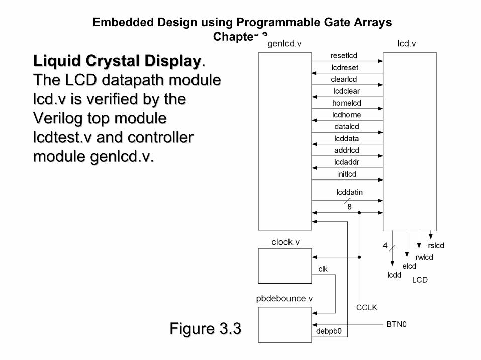
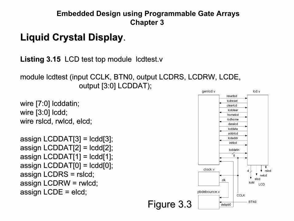
Liquid Crystal DisplayLiquid Crystal Display..The LCD datapath moduleThe LCD datapath modulelcd.vlcd.v is verified by theis verified by theVerilog top moduleVerilog top modulelcdtest.vlcdtest.v and controllerand controllermodule module genlcd.vgenlcd.v..
Figure 3.3Figure 3.3

Embedded Design using Programmable Gate ArraysChapter 3
Liquid Crystal DisplayLiquid Crystal Display..The wire net type establishesThe wire net type establishesthe 8the 8--bit and 4bit and 4--bit vectorbit vectorconnectivity for connectivity for lcddatinlcddatinand lcdd between theand lcdd between thelcd.vlcd.v and and genlcd.vgenlcd.v modules. modules.
Figure 3.3Figure 3.3

Embedded Design using Programmable Gate ArraysChapter 3
Liquid Crystal DisplayLiquid Crystal Display..The LCD external control|The LCD external control|signals LCDDAT[0],signals LCDDAT[0],LCDDAT[1], LCDDAT[2],LCDDAT[1], LCDDAT[2],LCDDAT[3], LCDRS,LCDDAT[3], LCDRS,LCDRW, and LCDE areLCDRW, and LCDE areassigned to internal datapathassigned to internal datapathregister signals lcdd[0],register signals lcdd[0],lcdd[1], lcdd[2], lcdd[3],lcdd[1], lcdd[2], lcdd[3],rslcdrslcd, , rwlcdrwlcd, and , and elcdelcd wherewherethey are then referenced inthey are then referenced inthe top module the top module lcdtest.vlcdtest.v..
Figure 3.3Figure 3.3

Embedded Design using Programmable Gate ArraysChapter 3
Liquid Crystal DisplayLiquid Crystal Display..Assignment of output signalsAssignment of output signalsto peripheral devices only into peripheral devices only inthe top module provides athe top module provides adegree of flexibility in thedegree of flexibility in theFPGA hardware synthesisFPGA hardware synthesisof an embedded systemof an embedded systemdesign.design.
Figure 3.3Figure 3.3

Embedded Design using Programmable Gate ArraysChapter 3
Liquid Crystal DisplayLiquid Crystal Display..The reset button BTN0 signalThe reset button BTN0 signalasynchronously initializes theasynchronously initializes theLCD controller signals.LCD controller signals.
The button is debounced byThe button is debounced bythe the pbdebounce.vpbdebounce.v module,module,
Figure 3.3Figure 3.3

Embedded Design using Programmable Gate ArraysChapter 3
Liquid Crystal DisplayLiquid Crystal Display..The The genlcd.vgenlcd.v module utilizesmodule utilizesan FSM as the LCD controlleran FSM as the LCD controllerto the LCD datapath moduleto the LCD datapath modulelcd.vlcd.v to reset and clear theto reset and clear theLCD, to set the DD RAMLCD, to set the DD RAMaddress to the second lineaddress to the second lineat position 5 and to send theat position 5 and to send the11 character ASCII string11 character ASCII stringhello worldhello world..
The state register The state register gstategstate setssetseach of the operations.each of the operations.
Figure 3.3Figure 3.3
Embedded Design using Programmable Gate ArraysChapter 3
Liquid Crystal DisplayLiquid Crystal Display..
Listing 3.15Listing 3.15 LCD test top module LCD test top module lcdtest.vlcdtest.v
module module lcdtestlcdtest (input CCLK, BTN0, output LCDRS, LCDRW, LCDE,(input CCLK, BTN0, output LCDRS, LCDRW, LCDE,output [3:0] LCDDAT);output [3:0] LCDDAT);
wire [7:0] wire [7:0] lcddatinlcddatin;;wire [3:0] lcdd;wire [3:0] lcdd;wire wire rslcdrslcd, , rwlcdrwlcd, , elcdelcd;;
assign LCDDAT[3] = lcdd[3];assign LCDDAT[3] = lcdd[3];assign LCDDAT[2] = lcdd[2];assign LCDDAT[2] = lcdd[2];assign LCDDAT[1] = lcdd[1];assign LCDDAT[1] = lcdd[1];assign LCDDAT[0] = lcdd[0];assign LCDDAT[0] = lcdd[0];assign LCDRS = assign LCDRS = rslcdrslcd;;assign LCDRW = assign LCDRW = rwlcdrwlcd;;assign LCDE = assign LCDE = elcdelcd;;
Figure 3.3Figure 3.3

Embedded Design using Programmable Gate ArraysChapter 3
Liquid Crystal DisplayLiquid Crystal Display..
lcd M0 (CCLK, lcd M0 (CCLK, resetlcdresetlcd, , clearlcdclearlcd, , homelcdhomelcd, , datalcddatalcd, , addrlcdaddrlcd, , lcdresetlcdreset, , lcdclearlcdclear, , lcdhomelcdhome, , lcddatalcddata, , cdaddrcdaddr, , rslcdrslcd, , rwlcdrwlcd, , elcdelcd, lcdd, , lcdd, lcddatinlcddatin, , initlcdinitlcd););
genlcdgenlcd M1 (CCLK, debpb0, M1 (CCLK, debpb0, resetlcdresetlcd, , clearlcdclearlcd,,homelcd,datalcdhomelcd,datalcd, , addrlcdaddrlcd, , initlcdinitlcd,,lcdresetlcdreset, , lcdclearlcdclear, , lcdhomelcdhome,,lcddatalcddata, , lcdaddrlcdaddr, , lcddatinlcddatin); );
pbdebouncepbdebounce M2 (M2 (clkclk, BTN0, debpb0);, BTN0, debpb0);clock M3 (CCLK, 25000, clock M3 (CCLK, 25000, clkclk););
endmoduleendmodule
Figure 3.3Figure 3.3

Embedded Design using Programmable Gate ArraysChapter 3
Liquid Crystal DisplayLiquid Crystal Display..
module module genlcd(inputgenlcd(input CCLK, debpb0, output reg CCLK, debpb0, output reg resetlcdresetlcd, output reg , output reg clearlcdclearlcd, , output reg output reg homelcdhomelcd, output reg , output reg datalcddatalcd, output reg , output reg addrlcdaddrlcd, , output reg output reg initlcdinitlcd, input , input lcdresetlcdreset, , lcdclearlcdclear, , lcdhomelcdhome, , lcddatalcddata, , lcdaddrlcdaddr, output reg [7:0] , output reg [7:0] lcddatinlcddatin););
reg [3:0] reg [3:0] gstategstate;; // state register// state registerreg [87:0] reg [87:0] strdatastrdata = "hello world";= "hello world"; // ASCII string // ASCII string integer i;integer i;
Figure 3.3Figure 3.3

Embedded Design using Programmable Gate ArraysChapter 3
Liquid Crystal DisplayLiquid Crystal Display..
always@(posedge CCLK)always@(posedge CCLK) // master clock event driven// master clock event drivenbeginbegin
if (debpb0 == 1)if (debpb0 == 1) // debounced push button reset// debounced push button resetbeginbegin
resetlcdresetlcd = 0;= 0;clearlcdclearlcd = 0;= 0;homelcdhomelcd = 0;= 0;datalcddatalcd = 0;= 0;gstategstate = 0;= 0;
endendelseelse
case (case (gstategstate))0:0: beginbegin
initlcdinitlcd = 1; // initialize LCD= 1; // initialize LCDgstategstate = 1;= 1;
endend

Embedded Design using Programmable Gate ArraysChapter 3
Liquid Crystal DisplayLiquid Crystal Display..
1:1: beginbegininitlcdinitlcd = 0;= 0;gstategstate = 2;= 2;
endend2:2: beginbegin
resetlcdresetlcd = 1; // reset LCD= 1; // reset LCDif (if (lcdresetlcdreset == 1)== 1)
beginbeginresetlcdresetlcd = 0;= 0;gstategstate = 3;= 3;
endendendend
3: 3: beginbegininitlcdinitlcd = 1;= 1;gstategstate = 4;= 4;
endend

Embedded Design using Programmable Gate ArraysChapter 3
Liquid Crystal DisplayLiquid Crystal Display. .
4:4: beginbegininitlcdinitlcd = 0;= 0;gstategstate = 5;= 5;
endend5: 5: beginbegin
clearlcdclearlcd = 1; // clear LCD= 1; // clear LCDif (if (lcdclearlcdclear == 1)== 1)
beginbeginclearlcdclearlcd = 0;= 0;gstategstate = 6;= 6;
endendendend
6: 6: beginbegininitlcdinitlcd = 1;= 1;gstategstate = 7;= 7;
endend

Embedded Design using Programmable Gate ArraysChapter 3
Liquid Crystal DisplayLiquid Crystal Display. .
7:7: beginbegininitlcdinitlcd = 0;= 0;gstategstate = 8;= 8;
endend8: 8: begin // DD RAM address 44hbegin // DD RAM address 44h
lcddatin[7:0] = 8'b01000100;lcddatin[7:0] = 8'b01000100;addrlcdaddrlcd = 1;= 1;if (if (lcdaddrlcdaddr == 1)== 1)
beginbeginaddrlcdaddrlcd = 0;= 0;gstategstate = 9;= 9;
endendendend
9:9: beginbegininitlcdinitlcd = 1;= 1;gstategstate = 10;= 10;
endend

Embedded Design using Programmable Gate ArraysChapter 3
Liquid Crystal DisplayLiquid Crystal Display. .
10: 10: beginbegininitlcdinitlcd = 0;= 0;i = 87; // character bit counti = 87; // character bit countgstategstate = 11;= 11;
endend11: 11: beginbegin // display string// display string
lcddatin[7:0] = strdata[ilcddatin[7:0] = strdata[i--:8];:8];datalcddatalcd = 1;= 1;if (if (lcddatalcddata == 1)== 1)
beginbegindatalcddatalcd = 0;= 0;gstategstate = 12;= 12;
endendendend
12: 12: beginbegininitlcdinitlcd = 1;= 1;gstategstate = 13;= 13;
endend

Embedded Design using Programmable Gate ArraysChapter 3
Liquid Crystal DisplayLiquid Crystal Display. .
13: 13: beginbegininitlcdinitlcd = 0;= 0;gstategstate = 14;= 14;
endend14: 14: beginbegin // loop until finished// loop until finished
i = i i = i –– 8;8;if (i < 0)if (i < 0)
gstategstate = 15;= 15;elseelse
gstategstate = 11;= 11;endend
15: 15: gstategstate = 15;= 15;default: default: gstategstate = 15;= 15;
endcaseendcaseendend
endmoduleendmodule

Embedded Design using Programmable Gate ArraysChapter 3
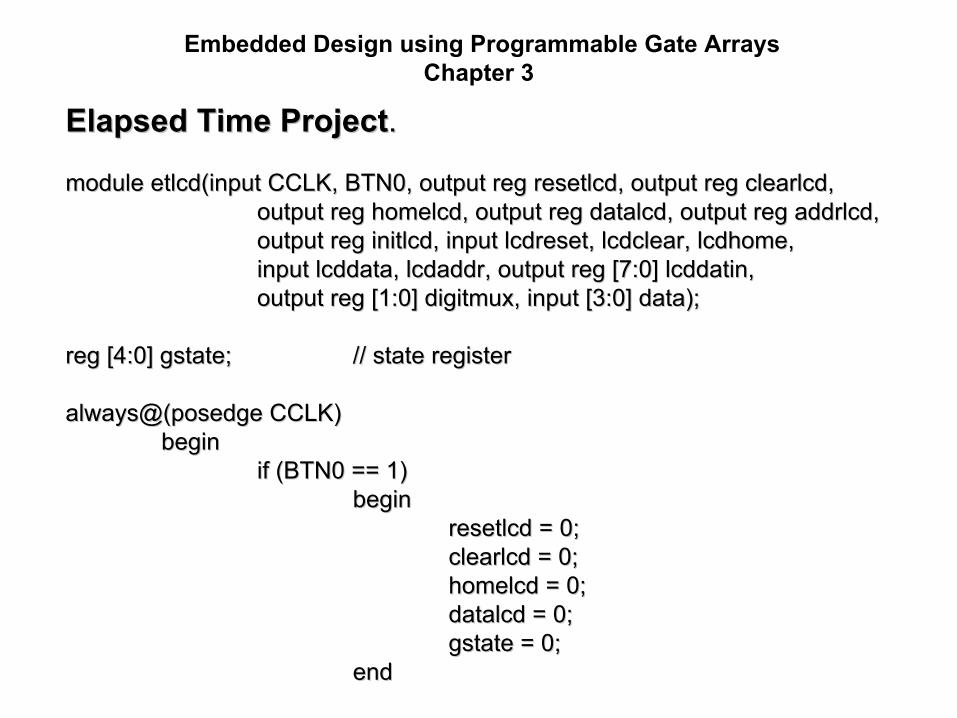
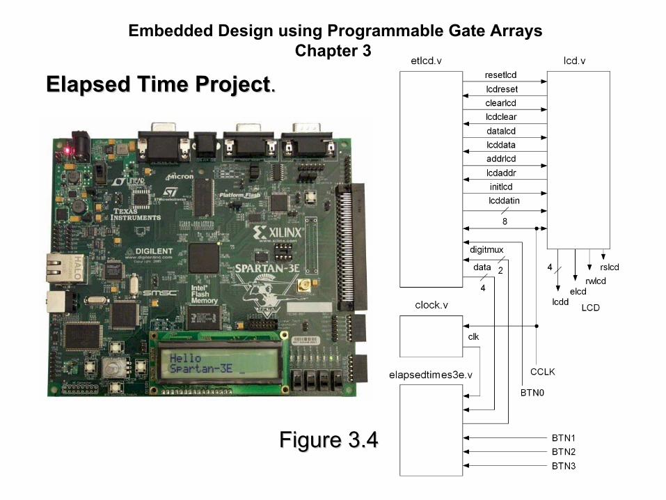
Elapsed Time ProjectElapsed Time Project..An elapsed time project canAn elapsed time project canexecute on the LCD of theexecute on the LCD of theSpartanSpartan--3E Starter Board. 3E Starter Board.
Figure 3.4Figure 3.4

Embedded Design using Programmable Gate ArraysChapter 3
Elapsed Time ProjectElapsed Time Project..An elapsed time project canAn elapsed time project canexecute on the LCD of theexecute on the LCD of theSpartanSpartan--3E Starter Board.3E Starter Board.
A wire net type establishes theA wire net type establishes the88--bit , 4bit , 4--bit and 2bit and 2--bit vectorbit vectorconnectivity for connectivity for lcddatinlcddatin, data,, data,lcdd and lcdd and digitmuxdigitmux between thebetween thelcd.vlcd.v, , elapsedtime.velapsedtime.v and and etlcd.vetlcd.vmodules. modules.
Figure 3.4Figure 3.4

Embedded Design using Programmable Gate ArraysChapter 3
Elapsed Time ProjectElapsed Time Project..The LCD external signalsThe LCD external signalsLCDDAT[0], LCDDAT[1],LCDDAT[0], LCDDAT[1],LCDDAT[2], LCDDAT[3], LCDRS,LCDDAT[2], LCDDAT[3], LCDRS,LCDRW, and LCDE are assignedLCDRW, and LCDE are assignedto internal controller signals to internal controller signals lcdd[0], lcdd[1], lcdd[2], lcdd[3],lcdd[0], lcdd[1], lcdd[2], lcdd[3],rslcdrslcd, , rwlcdrwlcd, and , and elcdelcd since theysince theyare only referenced in the topare only referenced in the topmodule s3eelapsedtime.v.module s3eelapsedtime.v.
Figure 3.4Figure 3.4

Embedded Design using Programmable Gate ArraysChapter 3
Elapsed Time ProjectElapsed Time Project..The reset button BTN0 signalThe reset button BTN0 signalasynchronously initializes theasynchronously initializes theLCD controller signals.LCD controller signals.
The The etlcd.vetlcd.v module is similar tomodule is similar tothe the genlcd.vgenlcd.v of Listing 3.15.of Listing 3.15.
Figure 3.4Figure 3.4

Embedded Design using Programmable Gate ArraysChapter 3
Elapsed Time ProjectElapsed Time Project..The The etlcd.vetlcd.v utilizes an FSM asutilizes an FSM asthe LCD controller to the LCDthe LCD controller to the LCDdatapath module datapath module lcd.vlcd.v to resetto resetand clear the LCD and set theand clear the LCD and set theDD RAM address to 46h or theDD RAM address to 46h or thesecond line at position 7 assecond line at position 7 aslisted in Table 3.1.listed in Table 3.1.
The state register The state register gstategstate setssetseach of the operations. each of the operations.
Figure 3.4Figure 3.4

Embedded Design using Programmable Gate ArraysChapter 3
Elapsed Time ProjectElapsed Time Project..
Listing 3.16Listing 3.16 Elapsed time top module for the SpartanElapsed time top module for the Spartan--3E Starter Board 3E Starter Board s3eelapsedtime.vs3eelapsedtime.v
module s3eelapsedtime (input CCLK, BTN0, BTN1, BTN2, BTN3, outpumodule s3eelapsedtime (input CCLK, BTN0, BTN1, BTN2, BTN3, output t LCDRS, LCDRW, LCDE, output [3:0] LCDDAT);LCDRS, LCDRW, LCDE, output [3:0] LCDDAT);
wire [3:0] data;wire [3:0] data;wire [1:0] digitmux;wire [1:0] digitmux;wire [7:0] lcddatin;wire [7:0] lcddatin;wire [3:0] lcdd;wire [3:0] lcdd;wire rslcd, rwlcd, elcd;wire rslcd, rwlcd, elcd;
assign LCDDAT[3] = lcdd[3];assign LCDDAT[3] = lcdd[3];assign LCDDAT[2] = lcdd[2];assign LCDDAT[2] = lcdd[2];assign LCDDAT[1] = lcdd[1];assign LCDDAT[1] = lcdd[1];assign LCDDAT[0] = lcdd[0];assign LCDDAT[0] = lcdd[0];

Embedded Design using Programmable Gate ArraysChapter 3
Elapsed Time ProjectElapsed Time Project..
assign LCDRS = assign LCDRS = rslcdrslcd;;assign LCDRW = assign LCDRW = rwlcdrwlcd;;assign LCDE = assign LCDE = elcdelcd;;
clock M0 (CCLK, 250000, clock M0 (CCLK, 250000, clkclk);); // 100 Hz// 100 Hzlcd M1 (CCLK, lcd M1 (CCLK, resetlcdresetlcd, , clearlcdclearlcd, , homelcdhomelcd, , datalcddatalcd, , addrlcdaddrlcd, , lcdresetlcdreset, ,
lcdclearlcdclear, , lcdhomelcdhome, , lcddatalcddata, , lcdaddrlcdaddr, , rslcdrslcd, , rwlcdrwlcd, , elcdelcd, lcdd, , lcdd, lcddatinlcddatin, , initlcdinitlcd););
elapsedtimes3e M2 (elapsedtimes3e M2 (clkclk, BTN1, BTN2, BTN3, , BTN1, BTN2, BTN3, digitmuxdigitmux, data);, data);etlcdetlcd M3 (CCLK, BTN0, M3 (CCLK, BTN0, resetlcdresetlcd, , clearlcdclearlcd, , homelcdhomelcd, , datalcddatalcd, , addrlcdaddrlcd, , initlcdinitlcd, ,
lcdresetlcdreset, , lcdclearlcdclear, , lcdhomelcdhome, , lcddatalcddata, , lcdaddrlcdaddr, , lcddatinlcddatin, , digitmuxdigitmux, , data);data);
endmoduleendmodule
Embedded Design using Programmable Gate ArraysChapter 3
Elapsed Time ProjectElapsed Time Project..
module module etlcd(inputetlcd(input CCLK, BTN0, output reg CCLK, BTN0, output reg resetlcdresetlcd, output reg , output reg clearlcdclearlcd, , output reg output reg homelcdhomelcd, output reg , output reg datalcddatalcd, output reg , output reg addrlcdaddrlcd, , output reg output reg initlcdinitlcd, input , input lcdresetlcdreset, , lcdclearlcdclear, , lcdhomelcdhome, , input input lcddatalcddata, , lcdaddrlcdaddr, output reg [7:0] , output reg [7:0] lcddatinlcddatin,,output reg [1:0] output reg [1:0] digitmuxdigitmux, input [3:0] data);, input [3:0] data);
reg [4:0] reg [4:0] gstategstate;; // state register// state register
always@(posedgealways@(posedge CCLK)CCLK)beginbegin
if (BTN0 == 1)if (BTN0 == 1)beginbegin
resetlcdresetlcd = 0;= 0;clearlcdclearlcd = 0;= 0;homelcdhomelcd = 0;= 0;datalcddatalcd = 0;= 0;gstategstate = 0;= 0;
endend

Embedded Design using Programmable Gate ArraysChapter 3
Elapsed Time ProjectElapsed Time Project..
elseelsecase (case (gstategstate))
0: begin0: begininitlcdinitlcd = 1;= 1;gstategstate = 1;= 1;
endend{LCD initialize, clear display and set display address continues{LCD initialize, clear display and set display address continues}}
11: begin11: beginlcddatin[7:4] = 3;lcddatin[7:4] = 3; // 30h// 30hdigitmuxdigitmux = 3;= 3; // sec10// sec10lcddatin[3:0] = data[3:0];lcddatin[3:0] = data[3:0];datalcddatalcd = 1;= 1;if (if (lcddatalcddata == 1)== 1)
beginbegindatalcddatalcd = 0;= 0;gstategstate = 12;= 12;
endendendend

Embedded Design using Programmable Gate ArraysChapter 3
Elapsed Time ProjectElapsed Time Project..
12: begin12: begininitlcdinitlcd = 1;= 1;gstategstate = 13;= 13;
endend13: begin13: begin
initlcdinitlcd = 0;= 0;gstategstate = 14;= 14;
endend14: begin14: begin
digitmuxdigitmux = 2;= 2; // sec1// sec1lcddatin[3:0] = data[3:0];lcddatin[3:0] = data[3:0];datalcddatalcd = 1;= 1;if (if (lcddatalcddata == 1)== 1)
beginbegindatalcddatalcd = 0; = 0; gstategstate = 15;= 15;
endendendend

Embedded Design using Programmable Gate ArraysChapter 3
Elapsed Time ProjectElapsed Time Project..15: begin15: begin
initlcdinitlcd = 1;= 1;gstategstate = 16;= 16;
endend16: begin16: begin
initlcdinitlcd = 0;= 0;gstategstate = 17;= 17;
endend17: begin17: begin
lcddatin[7:0] = 58;lcddatin[7:0] = 58; //ASCII //ASCII ::datalcddatalcd = 1;= 1;if (if (lcddatalcddata == 1)== 1)
beginbegindatalcddatalcd = 0;= 0;gstategstate = 18;= 18;
endendendend

Embedded Design using Programmable Gate ArraysChapter 3
Elapsed Time ProjectElapsed Time Project..18: begin18: begin
initlcdinitlcd = 1;= 1;gstategstate = 19;= 19;
endend19: begin19: begin
initlcdinitlcd = 0;= 0;gstategstate = 20;= 20;
endend20: begin20: begin
lcddatin[7:4] = 3;lcddatin[7:4] = 3; // 30h// 30hdigitmuxdigitmux = 1;= 1; // csec10// csec10lcddatin[3:0] = data[3:0];lcddatin[3:0] = data[3:0];datalcddatalcd = 1;= 1;if (if (lcddatalcddata == 1)== 1)
beginbegindatalcddatalcd = 0;= 0;gstategstate = 21;= 21;
endendendend

Embedded Design using Programmable Gate ArraysChapter 3
Elapsed Time ProjectElapsed Time Project..21: begin21: begin
initlcdinitlcd = 1;= 1;gstategstate = 22;= 22;
endend22: begin22: begin
initlcdinitlcd = 0;= 0;gstategstate = 23;= 23;
endend23: begin23: begin
digitmuxdigitmux = 0;= 0; // csec100// csec100lcddatin[3:0] = data[3:0];lcddatin[3:0] = data[3:0];datalcddatalcd = 1;= 1;if (if (lcddatalcddata == 1)== 1)
beginbegindatalcddatalcd = 0;= 0;gstategstate = 6;= 6;
endendendend

Embedded Design using Programmable Gate ArraysChapter 3
Elapsed Time ProjectElapsed Time Project..default: default: gstategstate = 0;= 0;
endcaseendcaseendend
endmoduleendmodule
Figure 3.4Figure 3.4

Embedded Design using Programmable Gate ArraysChapter 3
Elapsed Time ProjectElapsed Time Project..The module elaspedtimes3e.v The module elaspedtimes3e.v Is given in Listing 3.17. An inputIs given in Listing 3.17. An input22--bit register signal bit register signal digitmuxdigitmux isisused here to select which digit isused here to select which digit isreturned to the controller modulereturned to the controller moduleetlcd.vetlcd.v..
Figure 3.4Figure 3.4

Embedded Design using Programmable Gate ArraysChapter 3
Elapsed Time ProjectElapsed Time Project..
Listing 3.17Listing 3.17 Elapsed time module for the SpartanElapsed time module for the Spartan--3E Starter Board 3E Starter Board elapsedtimes3e.velapsedtimes3e.v
module elapsedtimes3e (input module elapsedtimes3e (input clkclk, BTN1, BTN2, BTN3, input [1:0] , BTN1, BTN2, BTN3, input [1:0] digitmuxdigitmux, , output reg [3:0] data);output reg [3:0] data);
reg reg startstopstartstop;; // start or stop// start or stopreg [3:0] csec100;reg [3:0] csec100; // seconds 1/100s// seconds 1/100sreg [3:0] csec10;reg [3:0] csec10; // seconds 1/10s// seconds 1/10sreg [3:0] sec1;reg [3:0] sec1; // seconds 1s// seconds 1sreg [3:0] sec10;reg [3:0] sec10; // seconds 10s// seconds 10s

Embedded Design using Programmable Gate ArraysChapter 3
Elapsed Time ProjectElapsed Time Project..
always@(digitmuxalways@(digitmux)) // digit multiplex even driven// digit multiplex even drivenbeginbegin
case (case (digitmuxdigitmux))0: 0: data[3:0] = csec100;data[3:0] = csec100;1:1: data[3:0] = csec10;data[3:0] = csec10;2: 2: data[3:0] = sec1;data[3:0] = sec1;3:3: data[3:0] = sec10;data[3:0] = sec10;
endcaseendcaseendend

Embedded Design using Programmable Gate ArraysChapter 3
Elapsed Time ProjectElapsed Time Project..
always@(posedgealways@(posedge clkclk)) // local clock event driven// local clock event drivenbeginbegin
if (BTN2 == 1)if (BTN2 == 1) // clear and stop// clear and stopbeginbegin
startstopstartstop = 0;= 0;csec100 = 0;csec100 = 0;csec10 = 0;csec10 = 0;sec1 = 0;sec1 = 0;sec10 = 0;sec10 = 0;
endend
if (BTN1 == 1)if (BTN1 == 1) // stop// stopstartstopstartstop=0;=0;
if (BTN3 == 1)if (BTN3 == 1) // start// startstartstopstartstop=1;=1;

Embedded Design using Programmable Gate ArraysChapter 3
Elapsed Time ProjectElapsed Time Project..
if (if (startstopstartstop == 1)== 1)beginbegin
csec100 = csec100 = csec100csec100 + 1;+ 1;
if (csec100 > 9)if (csec100 > 9)beginbegin
csec100 = 0;csec100 = 0;csec10 = csec10 = csec10csec10 + 1;+ 1;
endendif (csec10 > 9)if (csec10 > 9)
beginbegincsec10 = 0;csec10 = 0;sec1 = sec1 = sec1sec1 + 1;+ 1;
endend
Embedded Design using Programmable Gate ArraysChapter 3
Elapsed Time ProjectElapsed Time Project..
Figure 3.4Figure 3.4

Embedded Design using Programmable Gate ArraysChapter 3
PS/2 Mouse ProjectPS/2 Mouse Project..
Figure 3.6Figure 3.6

Embedded Design using Programmable Gate ArraysChapter 3
PS/2 Keyboard ProjectPS/2 Keyboard Project..
Figure 3.6Figure 3.6

Embedded Design using Programmable Gate ArraysChapter 3
PS/2 Mouse ProjectPS/2 Mouse Project..
Figure 3.7Figure 3.7

Embedded Design using Programmable Gate ArraysChapter 3
PGA and ADC ProjectPGA and ADC Project..
Figure 3.9Figure 3.9

End of Chapter 3End of Chapter 3
Programmable GateProgrammable GateArray HardwareArray Hardware