Eddy Current Techniques in NDEEddy Current … · Transformer AnalogTransformer Analog •...
106
Eddy Current Techniques in NDE Eddy Current Techniques in NDE Eddy Current Techniques in NDE Eddy Current Techniques in NDE Lalita Udpa Nondestructive Evaluation Laboratory Department of Electrical and Computer Engineering Michigan State University East Lansing, MI 48824 WCNDT P f W kh D b A il 15 2012 WCNDT Preconference Workshop, Durban, April 15, 2012
Transcript of Eddy Current Techniques in NDEEddy Current … · Transformer AnalogTransformer Analog •...

Eddy Current Techniques in NDEEddy Current Techniques in NDEEddy Current Techniques in NDEEddy Current Techniques in NDE
Lalita UdpaNondestructive Evaluation Laboratory
Department of Electrical and Computer EngineeringMichigan State Universityc g S e U ve s yEast Lansing, MI 48824
WCNDT P f W k h D b A il 15 2012WCNDT Preconference Workshop, Durban, April 15, 2012
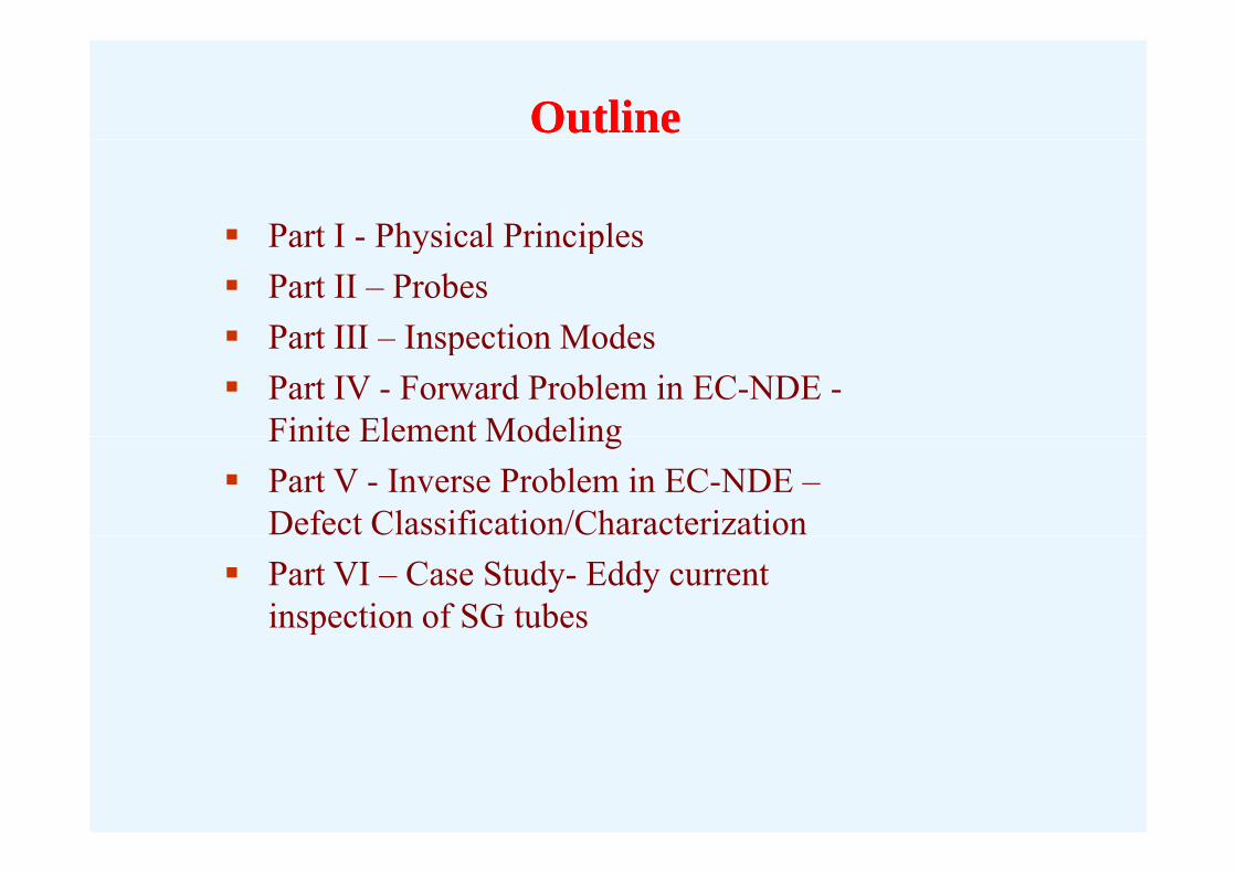
OutlineOutline
Part I - Physical Principles Part I - Physical Principles Part II – Probes Part III Inspection Modes Part III – Inspection Modes Part IV - Forward Problem in EC-NDE -
Finite Element ModelingFinite Element Modeling Part V - Inverse Problem in EC-NDE –
Defect Classification/Characterization Part VI – Case Study- Eddy current
inspection of SG tubesp
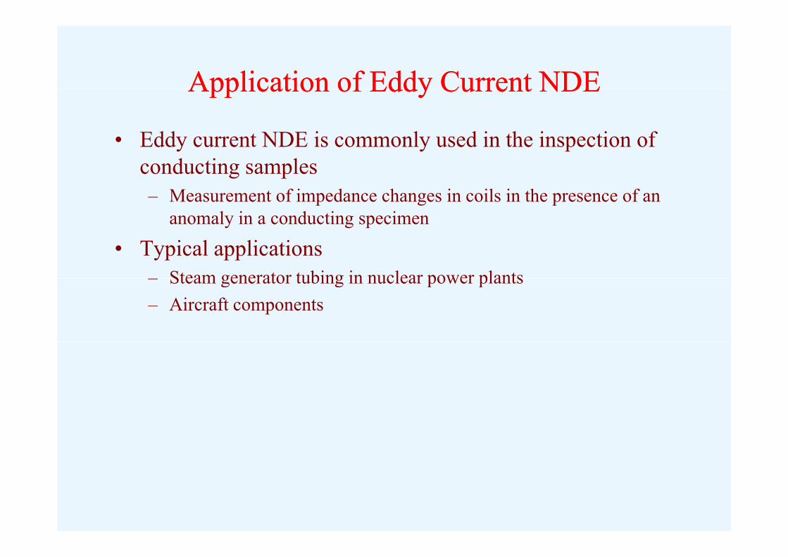
Application of Eddy Current NDEApplication of Eddy Current NDEApplication of Eddy Current NDEApplication of Eddy Current NDE
• Eddy current NDE is commonly used in the inspection of conducting samples– Measurement of impedance changes in coils in the presence of an
l i d ti ianomaly in a conducting specimen
• Typical applicationsSteam generator tubing in nuclear power plants– Steam generator tubing in nuclear power plants
– Aircraft components

N l P I d t• Nuclear Power Industry–Inspection of Steam Generator Tubing in Nuclear Power Plants
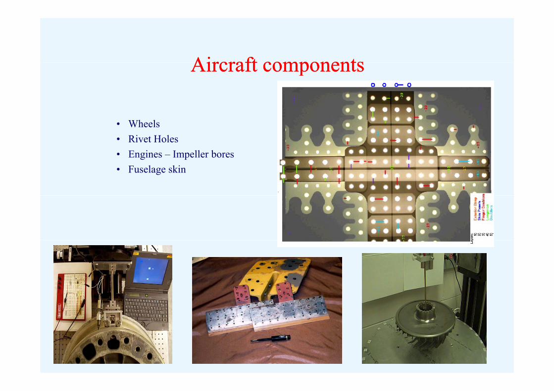
Aircraft componentsAircraft componentsAircraft componentsAircraft components
• Wheels• Rivet Holes
E i I ll b• Engines – Impeller bores• Fuselage skin

Part IPart I -- Physical PrinciplesPhysical PrinciplesPart I Part I Physical PrinciplesPhysical Principles
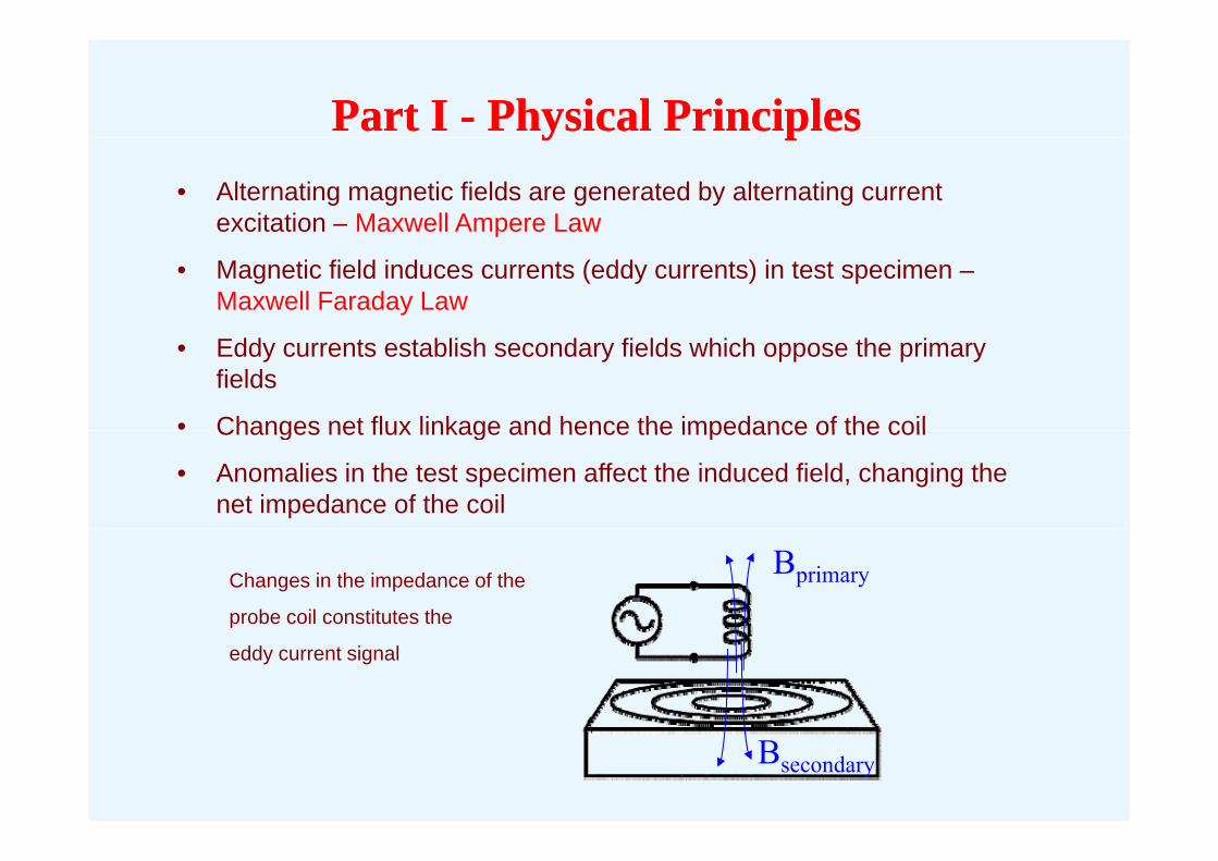
Part I Part I -- Physical PrinciplesPhysical Principles• Alternating magnetic fields are generated by alternating current
excitation – Maxwell Ampere Law
y py p
p
• Magnetic field induces currents (eddy currents) in test specimen –Maxwell Faraday Law
• Eddy currents establish secondary fields which oppose the primary fields
• Changes net flux linkage and hence the impedance of the coilChanges net flux linkage and hence the impedance of the coil
• Anomalies in the test specimen affect the induced field, changing the net impedance of the coil
Changes in the impedance of the
probe coil constitutes the
Bprimary
p
eddy current signal
Bsecondary
Physical PrinciplesPhysical Principlesy py p
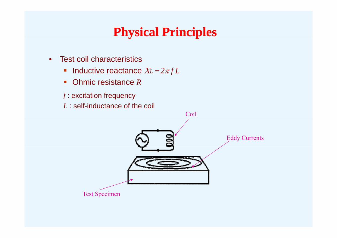
• Test coil characteristics Inductive reactance L 2 f L Ohmic resistance Rf : excitation frequencyL : self-inductance of the coil
Coil
Eddy Currents
Test Specimen
Eddy Current InspectionEddy Current Inspectiony py p
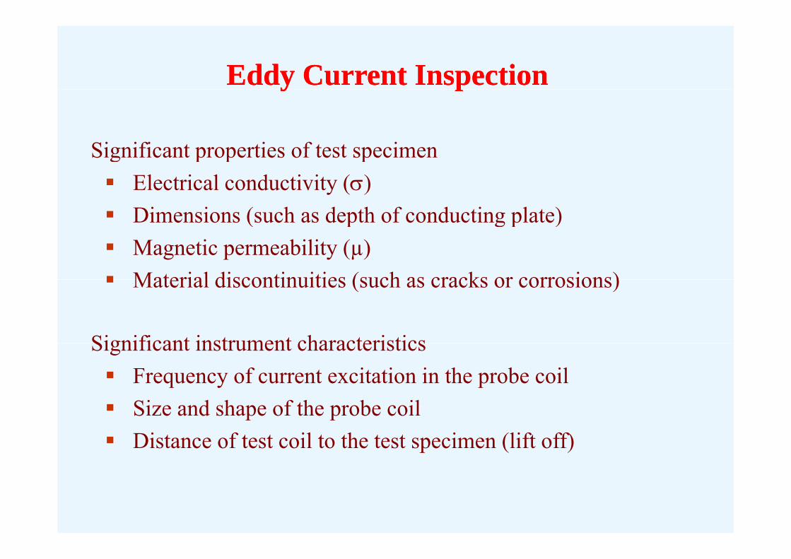
Significant properties of test specimenSignificant properties of test specimen Electrical conductivity () Dimensions (such as depth of conducting plate) Dimensions (such as depth of conducting plate) Magnetic permeability (µ) Material discontinuities (such as cracks or corrosions) Material discontinuities (such as cracks or corrosions)
Significant instrument characteristicsSignificant instrument characteristics Frequency of current excitation in the probe coil Size and shape of the probe coil Size and shape of the probe coil Distance of test coil to the test specimen (lift off)
Transformer AnalogTransformer AnalogTransformer AnalogTransformer Analog
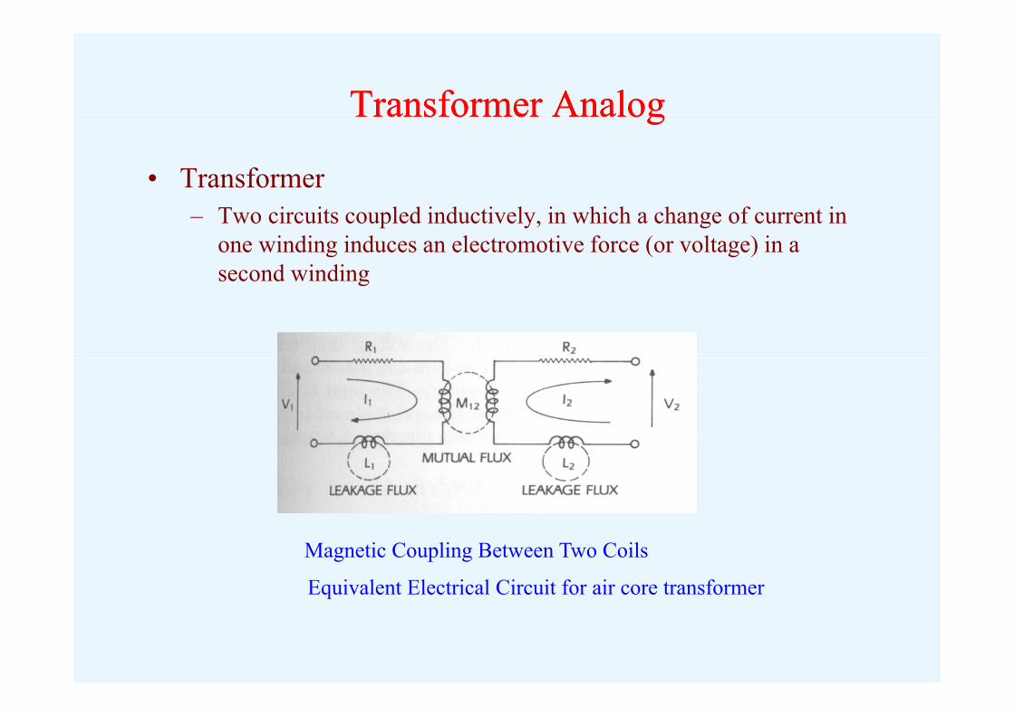
• Transformer– Two circuits coupled inductively, in which a change of current in
one winding induces an electromotive force (or voltage) in a second windingsecond winding
Magnetic Coupling Between Two Coils
Equivalent Electrical Circuit for air core transformer
Eddy Current Inspection Eddy Current Inspection -- Transformer AnalogTransformer Analog
When two coils are coupled by a magnetic field, they are subject to
y py p gg
W e wo co s e coup ed by g e c e d, ey e subjec othe effects of a mutual inductance.
N N
1
122
1
1212 I
NI
M
2
211
2
2121 I
NI
M
hwhere
2112 MM mutual inductance of two coils (henrys)2112
)or ( 2112 flux linkage created by flux of coil-1 passing through the interior of coil-2 (reverse vise)
b f i il ( il ))or ( 21 NN
)(
number of turns in coil-1 (coil-2)
current flow in coil-1 (coil-2)
t l fl t d b t i il 1 d i)or ( 11 II
)or ( 2112 mutual flux created by current in coil-1 and passing though interior of coil-2 (reverse vise)
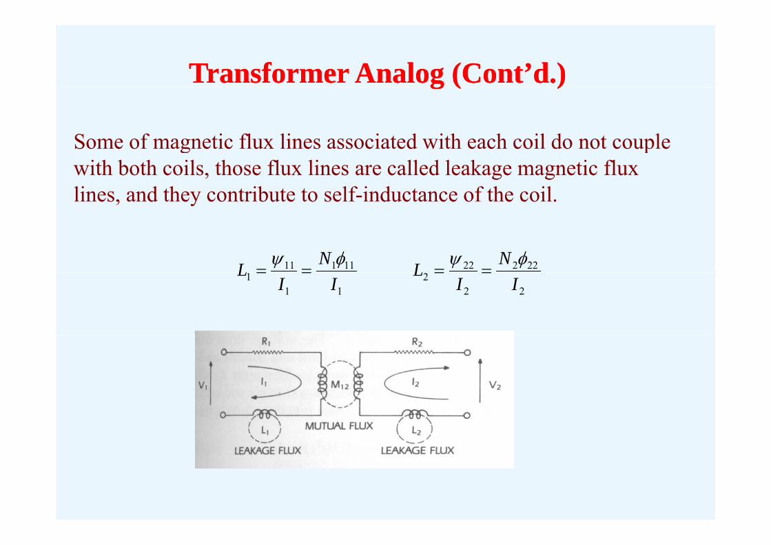
Transformer Analog (Cont’d.)Transformer Analog (Cont’d.)
Some of magnetic flux lines associated with each coil do not couple
g ( )g ( )
So e o g e c u es ssoc ed w e c co do o coup ewith both coils, those flux lines are called leakage magnetic flux lines, and they contribute to self-inductance of the coil.
11111 NL 22222 NL
11
1 IIL
222 II
L
Transformer AnalogTransformer Analog (Cont’d.)(Cont’d.)gg ( )( )
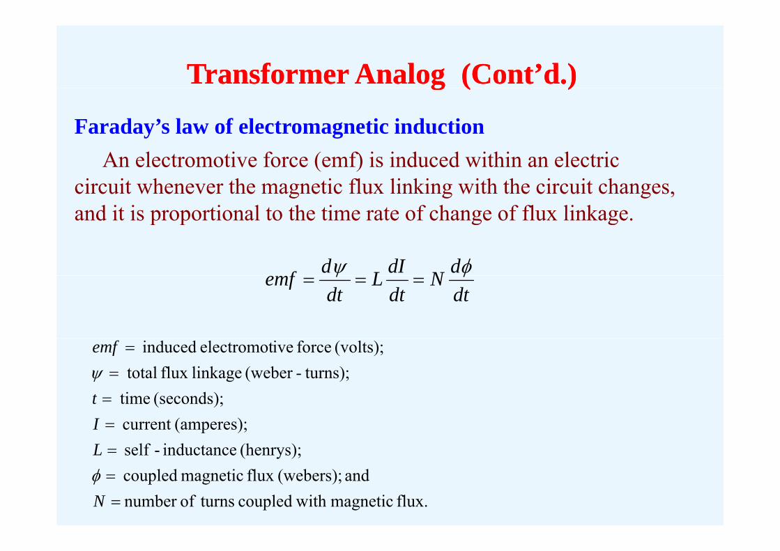
Faraday’s law of electromagnetic inductionAn electromotive force (emf) is induced within an electric
circuit whenever the magnetic flux linking with the circuit changes, and it is proportional to the time rate of change of flux linkageand it is proportional to the time rate of change of flux linkage.
dNdILdf dt
Ndt
Ldt
emf
(seconds);timeturns);-(weber linkageflux total
(volts);forceiveelectromot induced
t
emf
(henrys); inductance-self (amperes);current
(seconds); time
LIt
flux. magnetic with coupled turnsofnumber and (webers);flux magnetic coupled
N
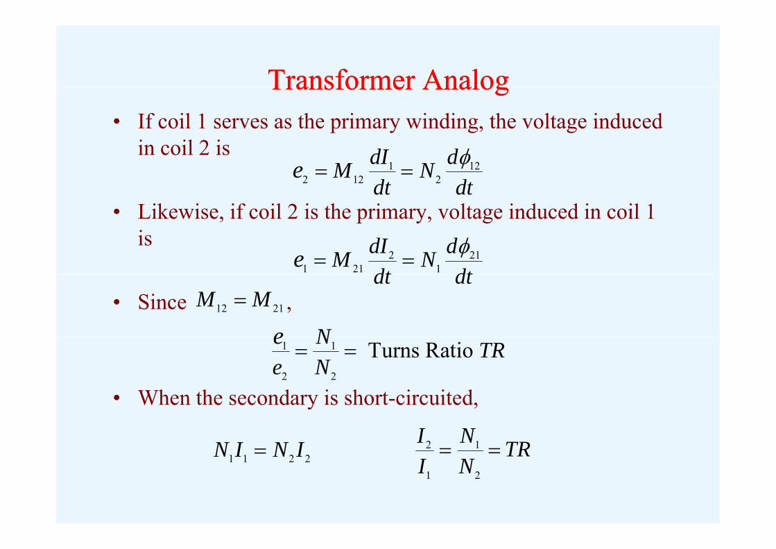
Transformer AnalogTransformer AnalogTransformer AnalogTransformer Analog• If coil 1 serves as the primary winding, the voltage induced
in coil 2 is dI din coil 2 is
• Likewise if coil 2 is the primary voltage induced in coil 1
1 122 12 2
dI dM Ndt dt
e
• Likewise, if coil 2 is the primary, voltage induced in coil 1 is
2 211 21 1
dI dM Ndt dt
e
• Since , dt dt
12 21M M
Ne
• When the secondary is short-circuited
1 1
2 2
Turns Ratio N TRe Ne
• When the secondary is short-circuited,
1 1 2 2N I N I 2 1I N TRI N 1 1 2 2
1 2I N
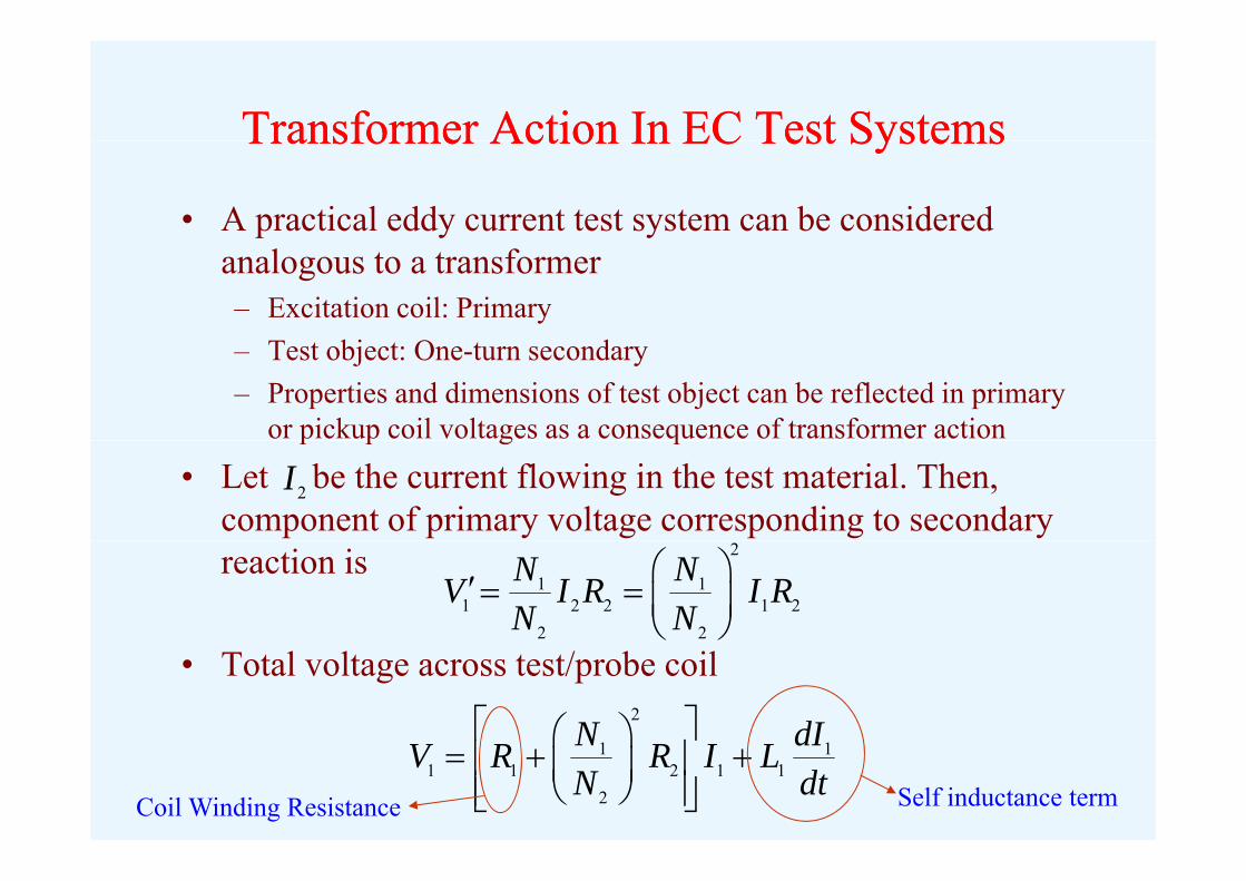
Transformer Action In EC Test SystemsTransformer Action In EC Test SystemsTransformer Action In EC Test SystemsTransformer Action In EC Test Systems
• A practical eddy current test system can be considered analogous to a transformer– Excitation coil: Primary
T bj O d– Test object: One-turn secondary– Properties and dimensions of test object can be reflected in primary
or pickup coil voltages as a consequence of transformer action p p g q
• Let be the current flowing in the test material. Then, component of primary voltage corresponding to secondary
2I
reaction is 2
1 11 2 2 1 2
2 2
N NV I R I RN N
• Total voltage across test/probe coil2
N dI 1 1
1 1 2 1 12
N dIV R R I LN dt
Self inductance termCoil Winding Resistance
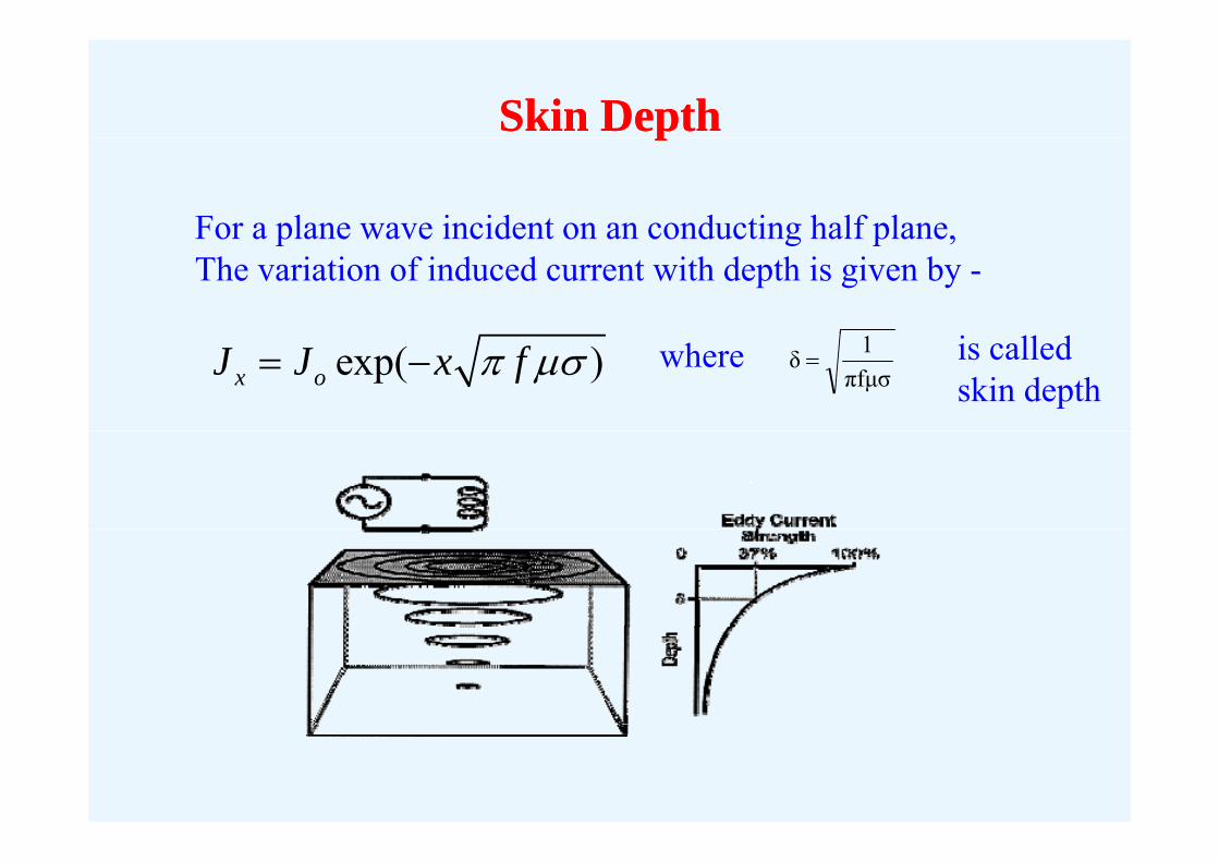
Skin DepthSkin Depthpp
For a plane wave incident on an conducting half plane,For a plane wave incident on an conducting half plane,The variation of induced current with depth is given by -
exp( )x oJ J x f πfμσ1δ where is called
skin depth
Factors Affecting Eddy Current Factors Affecting Eddy Current MeasurementsMeasurements
• Factors affecting eddy current transducers– Lift-off: Separation between the coil and the specimen surface
• Impedance of the coil changes as the probe is moved from air till it touches the material surface – liftoff curve
• Minimized by the use of surface-riding probes or multifrequency measurements
• Can be used to determine the thickness of non-conducting coatings on conducting surfaces
– Skin effect• Eddy currents decay exponentially with depth in the material• Standard depth of penetration: (depth at which eddy currents become
1/e the surface value)• This limits the sensitivity of eddy current method to the surface of the
conducting specimen
Part II Part II -- Eddy Current SensorsEddy Current Sensorsyy
Part II Part II -- Eddy Current SensorsEddy Current Sensorsyy
Absolute probe Absolute probe
Differential Bobbin probe
Plus Point & Array Probe
Meandering coilMeandering coil
Eddy Current – Magneto-optic (MOI) sensor
Eddy Current – Magneto-resistive (MR) sensor
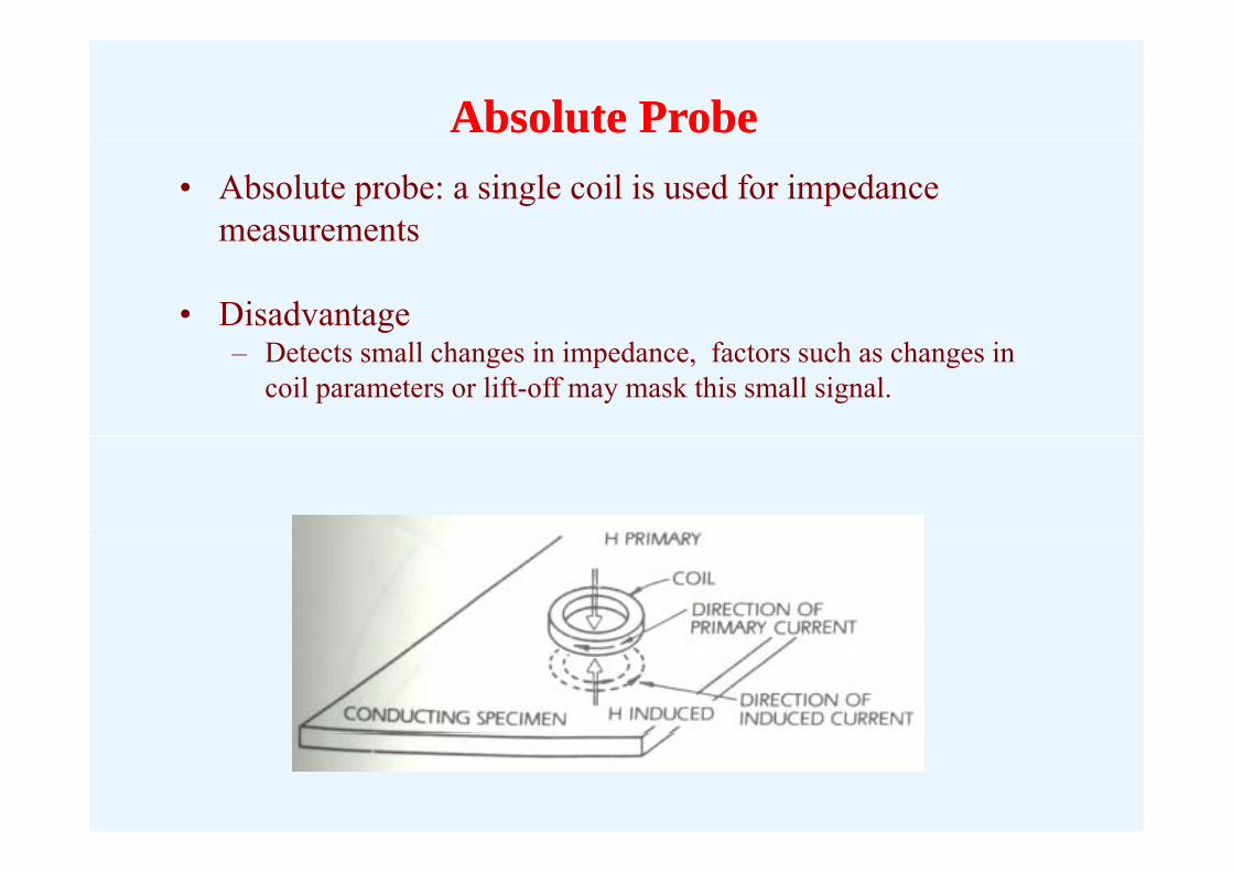
Absolute ProbeAbsolute Probe• Absolute probe: a single coil is used for impedance
measurementsmeasurements
• Disadvantage – Detects small changes in impedance, factors such as changes in
coil parameters or lift-off may mask this small signal.
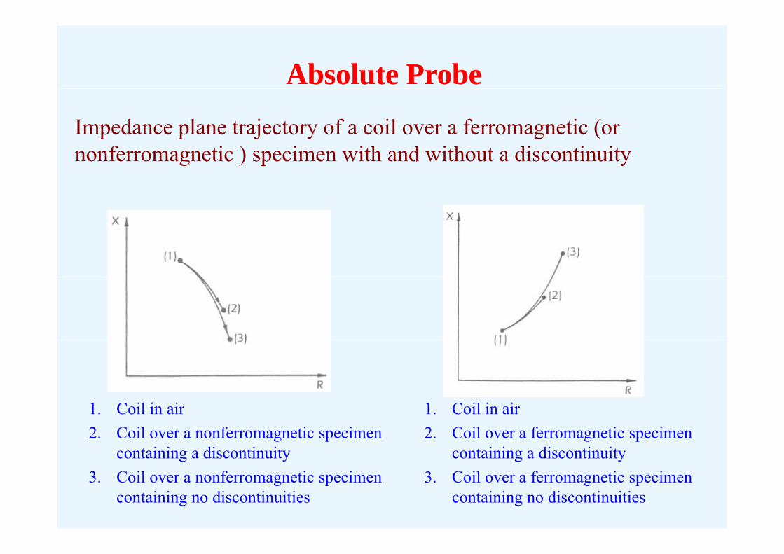
Absolute ProbeAbsolute Probe
Impedance plane trajectory of a coil over a ferromagnetic (or nonferromagnetic ) specimen with and without a discontinuitynonferromagnetic ) specimen with and without a discontinuity
1 C il i i1 C il i i 1. Coil in air2. Coil over a ferromagnetic specimen
containing a discontinuity
1. Coil in air2. Coil over a nonferromagnetic specimen
containing a discontinuity3. Coil over a ferromagnetic specimen
containing no discontinuities3. Coil over a nonferromagnetic specimen
containing no discontinuities
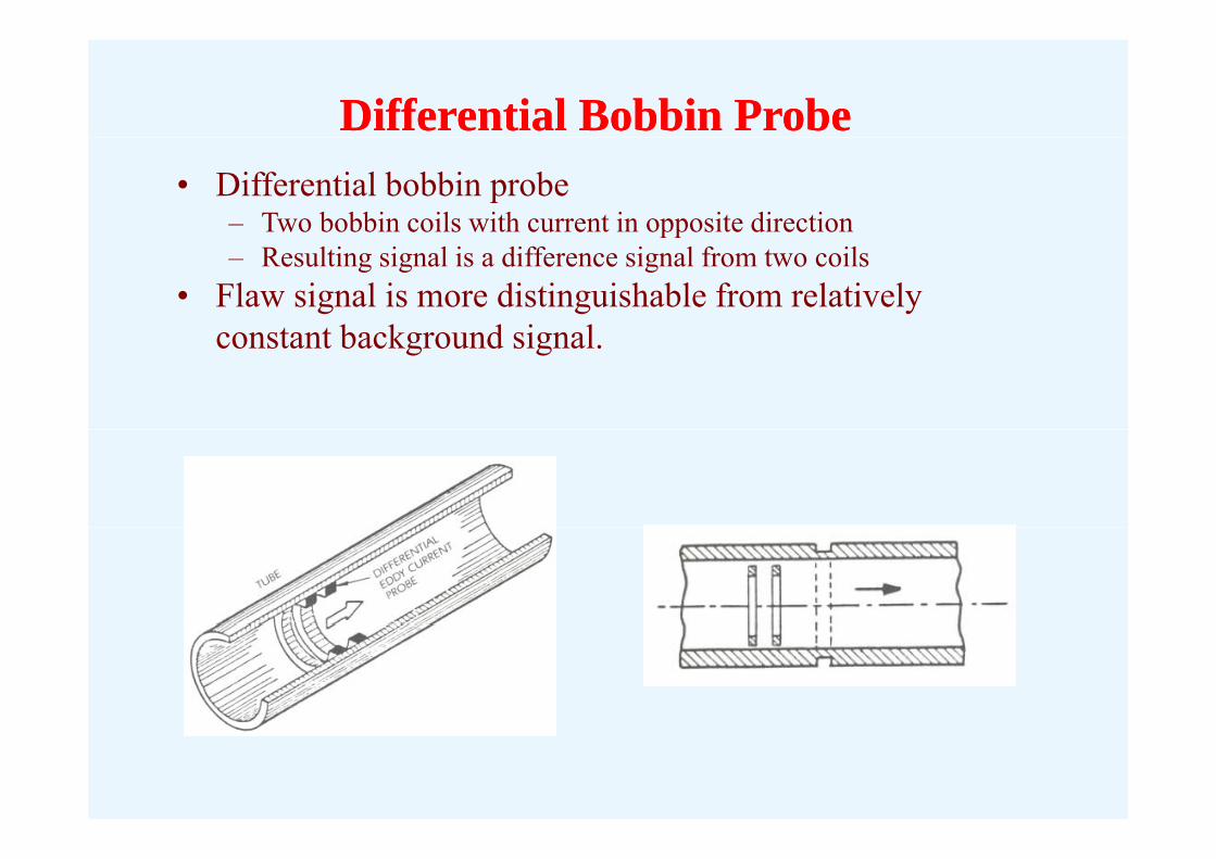
Differential Bobbin ProbeDifferential Bobbin Probe• Differential bobbin probe
– Two bobbin coils with current in opposite directionpp– Resulting signal is a difference signal from two coils
• Flaw signal is more distinguishable from relatively t t b k d i lconstant background signal.
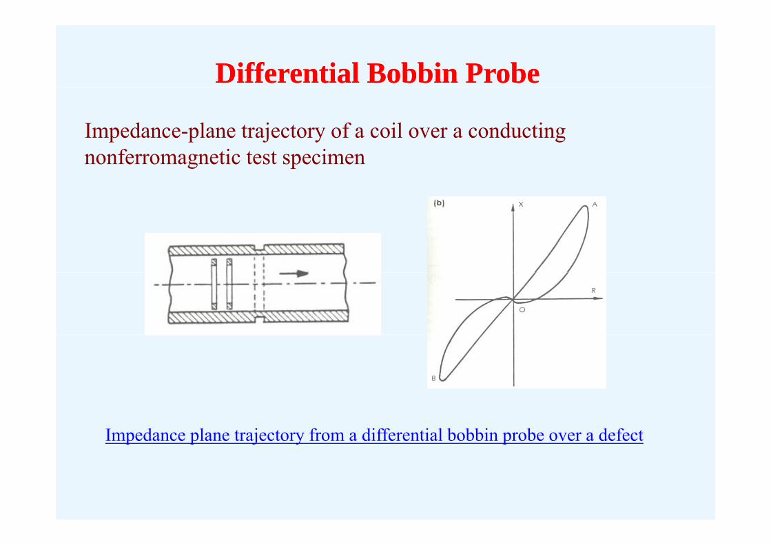
Differential Bobbin ProbeDifferential Bobbin Probe
Impedance-plane trajectory of a coil over a conducting f i inonferromagnetic test specimen
Impedance plane trajectory from a differential bobbin probe over a defect
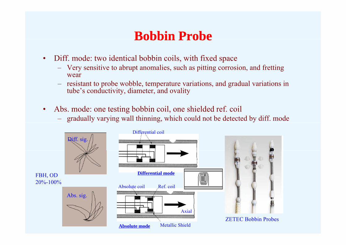
Bobbin ProbeBobbin ProbeBobbin ProbeBobbin Probe• Diff. mode: two identical bobbin coils, with fixed space
Very sensitive to abrupt anomalies such as pitting corrosion and fretting– Very sensitive to abrupt anomalies, such as pitting corrosion, and fretting wear
– resistant to probe wobble, temperature variations, and gradual variations in tube’s conductivity, diameter, and ovality
• Abs. mode: one testing bobbin coil, one shielded ref. coil– gradually varying wall thinning, which could not be detected by diff. mode
Differential coilDiff. sig.
Differential modeFBH, OD
Ref. coilAbsolute coil
Abs. sig.
20%-100%
Metallic Shield
Axial
Absolute modeZETEC Bobbin Probes
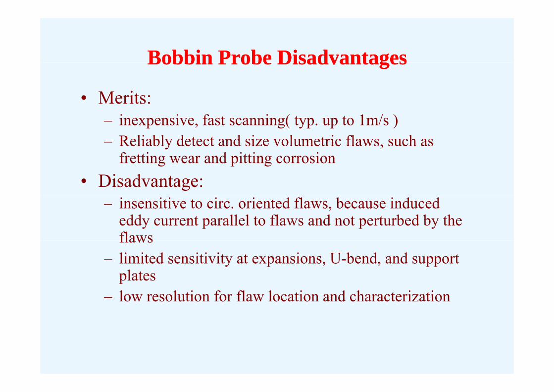
Bobbin Probe DisadvantagesBobbin Probe DisadvantagesBobbin Probe DisadvantagesBobbin Probe Disadvantages
• Merits: – inexpensive, fast scanning( typ. up to 1m/s )– Reliably detect and size volumetric flaws, such as
fretting wear and pitting corrosion• Disadvantage:
– insensitive to circ. oriented flaws, because induced eddy current parallel to flaws and not perturbed by the flawsflaws
– limited sensitivity at expansions, U-bend, and support plates
– low resolution for flaw location and characterization
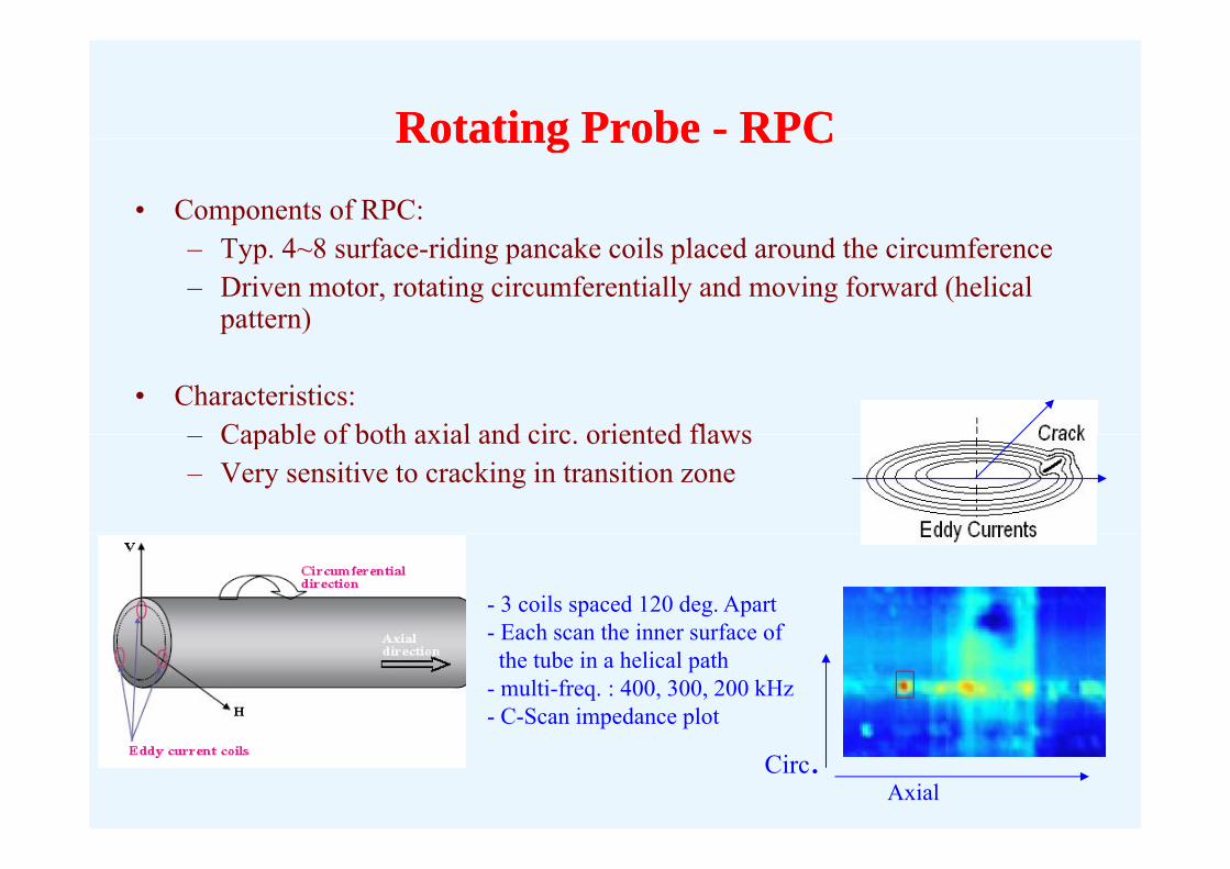
Rotating ProbeRotating Probe -- RPCRPCRotating Probe Rotating Probe RPCRPC• Components of RPC:
– Typ. 4~8 surface-riding pancake coils placed around the circumference– Driven motor, rotating circumferentially and moving forward (helical
pattern)
• Characteristics:Capable of both axial and circ oriented flaws– Capable of both axial and circ. oriented flaws
– Very sensitive to cracking in transition zone
- 3 coils spaced 120 deg. ApartEach scan the inner surface of- Each scan the inner surface of the tube in a helical path
- multi-freq. : 400, 300, 200 kHz- C-Scan impedance plot
AxialCirc.
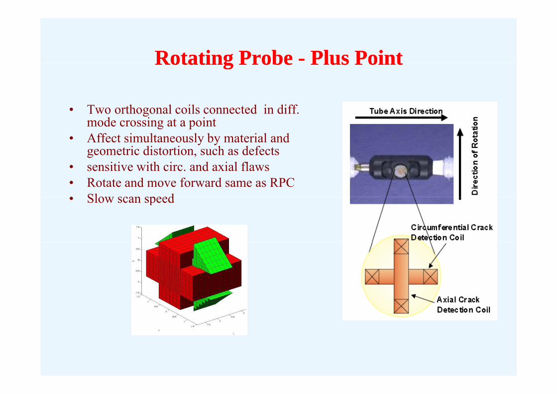
Rotating ProbeRotating Probe -- Plus PointPlus PointRotating Probe Rotating Probe Plus PointPlus Point
T o orthogonal coils connected in diff• Two orthogonal coils connected in diff. mode crossing at a point
• Affect simultaneously by material and geometric distortion such as defectsgeometric distortion, such as defects
• sensitive with circ. and axial flaws• Rotate and move forward same as RPC• Slow scan speed• Slow scan speed
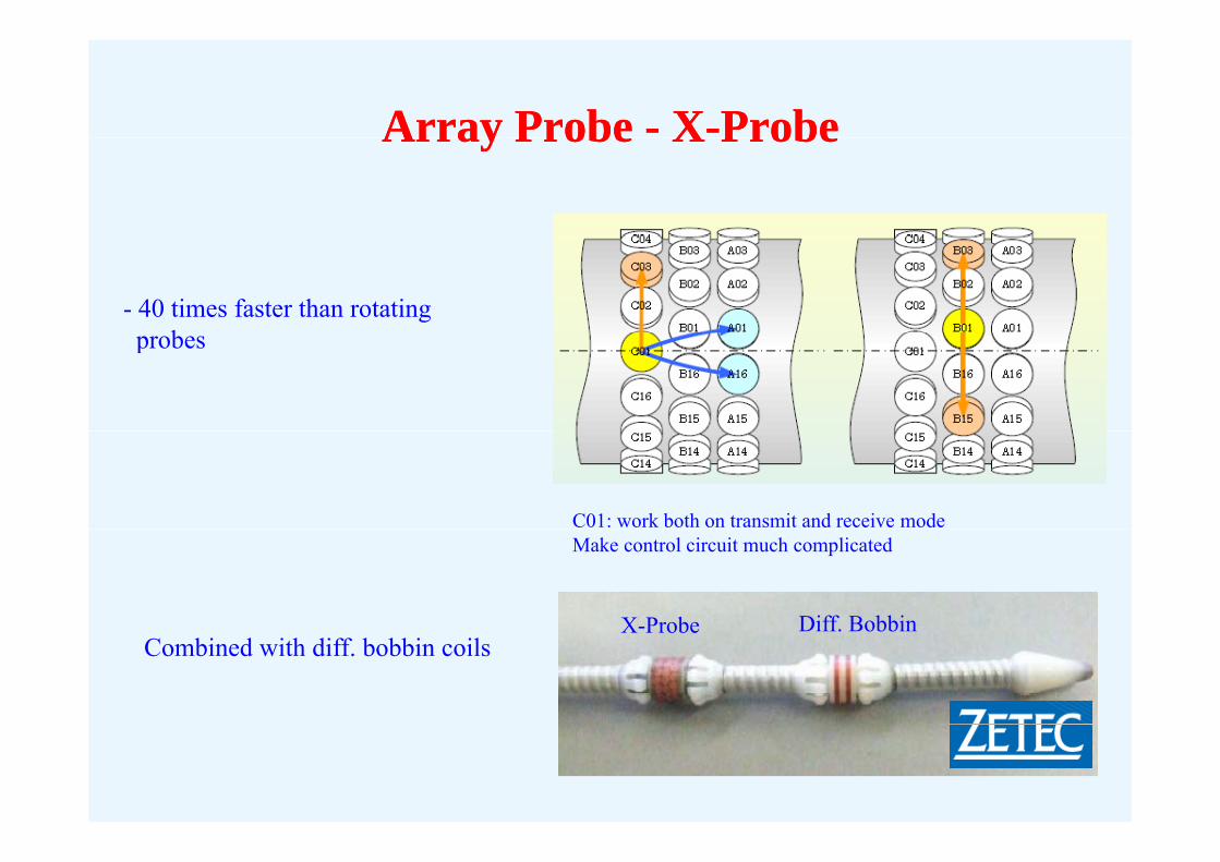
Array ProbeArray Probe -- XX--ProbeProbeArray Probe Array Probe XX ProbeProbe
- 40 times faster than rotatingbprobes
C01: work both on transmit and receive mode
Diff BobbinX-Probe
Make control circuit much complicated
Combined with diff. bobbin coilsDiff. BobbinX-Probe
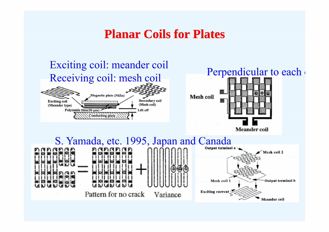
Planar Coils for PlatesPlanar Coils for PlatesPlanar Coils for PlatesPlanar Coils for Plates
E citing coil: meander coilExciting coil: meander coilReceiving coil: mesh coil Perpendicular to each o
S Yamada etc 1995 Japan and CanadaS. Yamada, etc. 1995, Japan and Canada
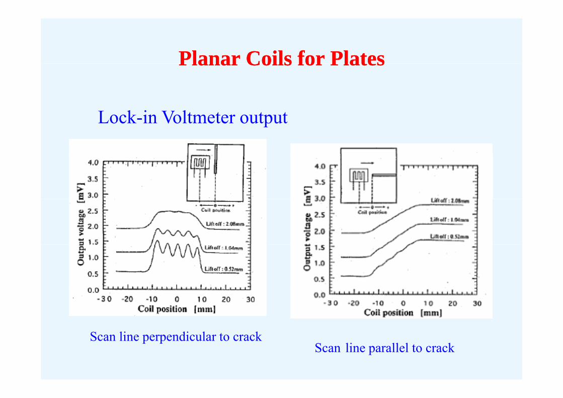
Planar Coils for PlatesPlanar Coils for PlatesPlanar Coils for PlatesPlanar Coils for Plates
Lock-in Voltmeter output
S li di l t kScan line perpendicular to crackScan line parallel to crack
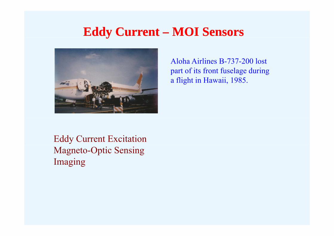
Eddy Current Eddy Current –– MOI SensorsMOI Sensorsyy
Aloha Airlines B-737-200 lost part of its front fuselage during a flight in Hawaii, 1985.
Eddy Current ExcitationMagneto-Optic SensingImaging
Operational Principles ofOperational Principles of MOIMOIOperational Principles ofOperational Principles of MOIMOI
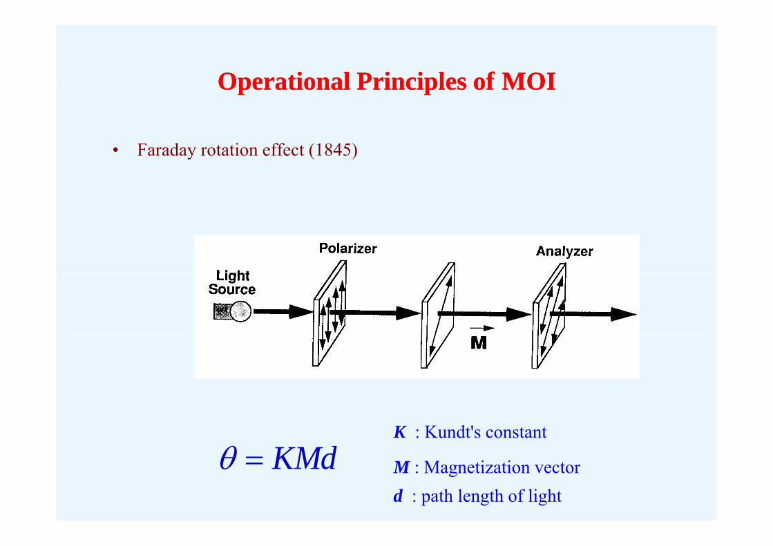
• Faraday rotation effect (1845)• Faraday rotation effect (1845)
K : Kundt's constant
KMd M : Magnetization vectord : path length of light
KMd
MagnetoMagneto--Optic SensorsOptic SensorsMagnetoMagneto Optic SensorsOptic Sensors
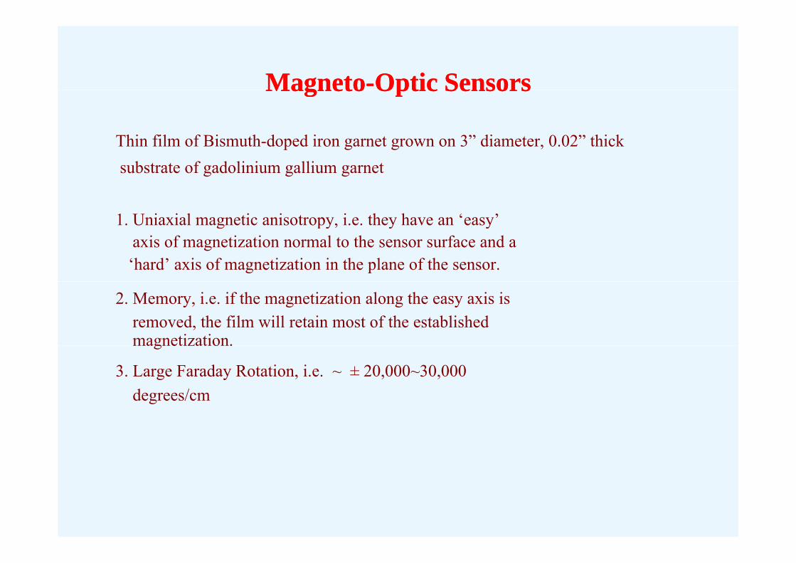
Thin film of Bismuth-doped iron garnet grown on 3” diameter, 0.02” thick substrate of gadolinium gallium garnet
1 Uniaxial magnetic anisotropy i e they have an ‘easy’1. Uniaxial magnetic anisotropy, i.e. they have an ‘easy’axis of magnetization normal to the sensor surface and a‘hard’ axis of magnetization in the plane of the sensor.
2. Memory, i.e. if the magnetization along the easy axis is removed, the film will retain most of the established magnetization.magnetization.
3. Large Faraday Rotation, i.e. ~ ± 20,000~30,000 degrees/cm
Eddy Current InductionEddy Current InductionEddy Current InductionEddy Current Induction
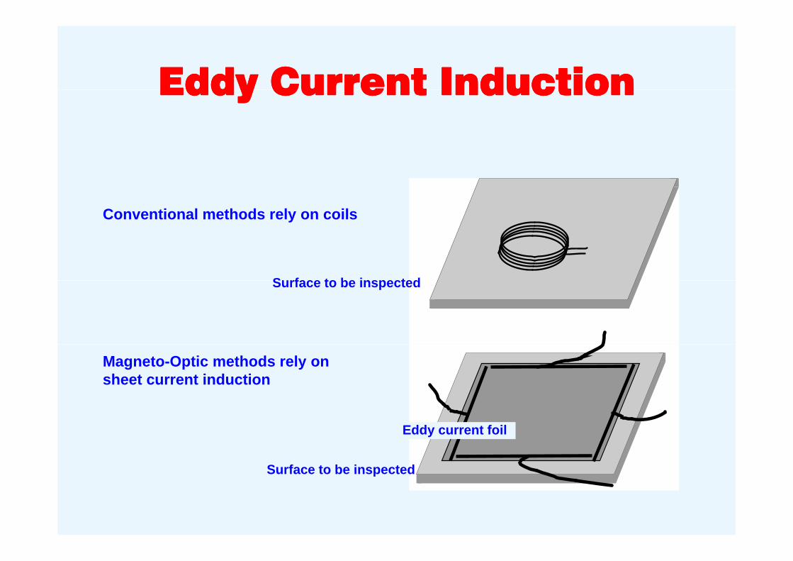
Conventional methods rely on coilsConventional methods rely on coils
Surface to be inspectedSurface to be inspected
Magneto-Optic methods rely onsheet current induction
Surface to be inspected
Eddy current foil
Surface to be inspected
MagnetoMagneto--Optic ImagingOptic ImagingMagnetoMagneto Optic ImagingOptic Imaging
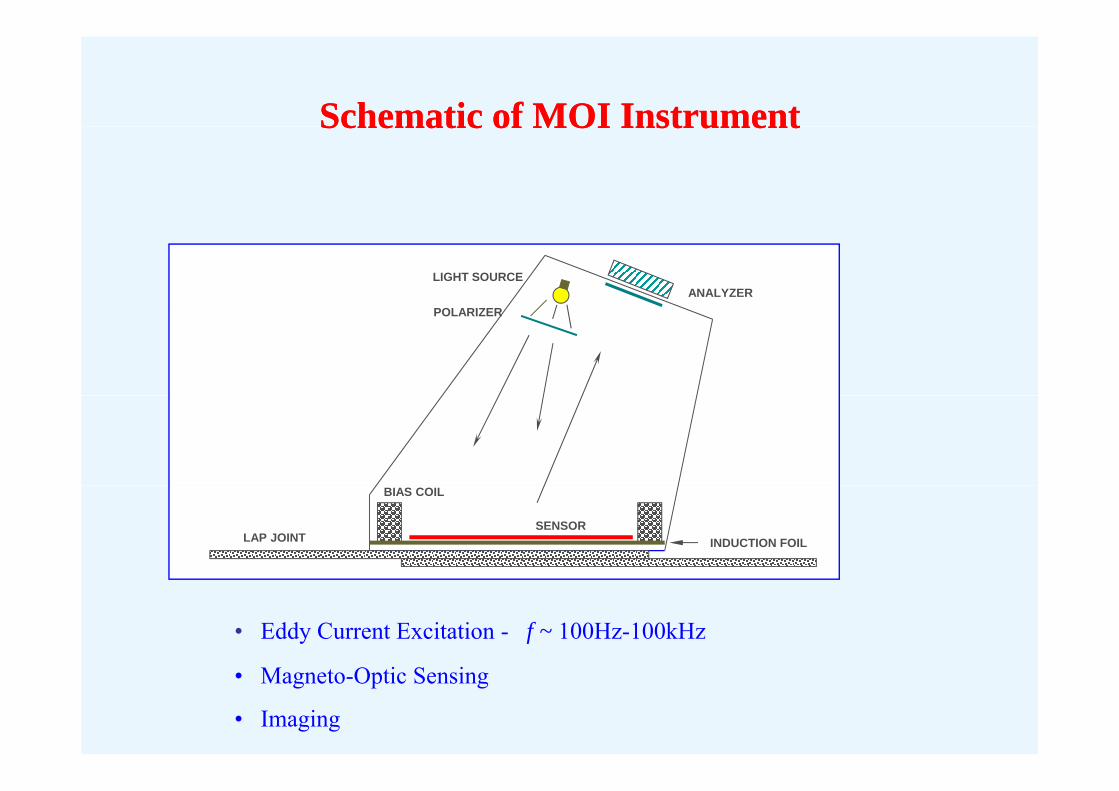
Schematic of MOI InstrumentSchematic of MOI InstrumentSchematic of MOI InstrumentSchematic of MOI Instrument
LIGHT SOURCEANALYZER
POLARIZER
LAP JOINT
BIAS COIL
SENSORINDUCTION FOIL
• Eddy Current Excitation - f ~ 100Hz-100kHz
• Magneto-Optic Sensing
• Imaging
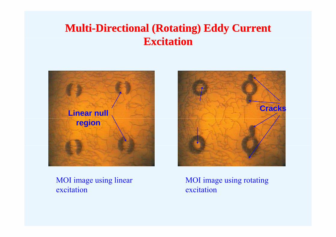
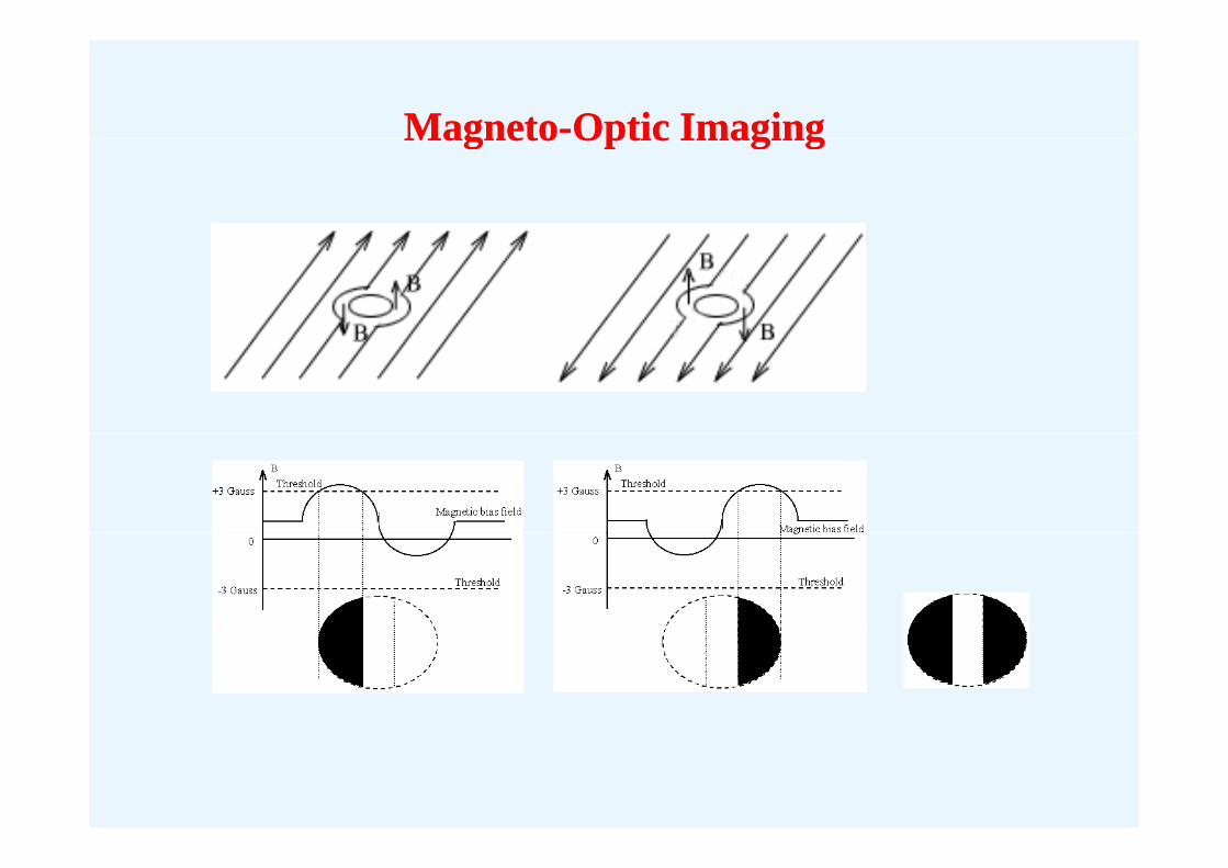
MultiMulti--Directional (Rotating) Eddy Current Directional (Rotating) Eddy Current E i iE i iExcitationExcitation
Linear null Cracks
region
MOI image using linear excitation
MOI image using rotating excitation
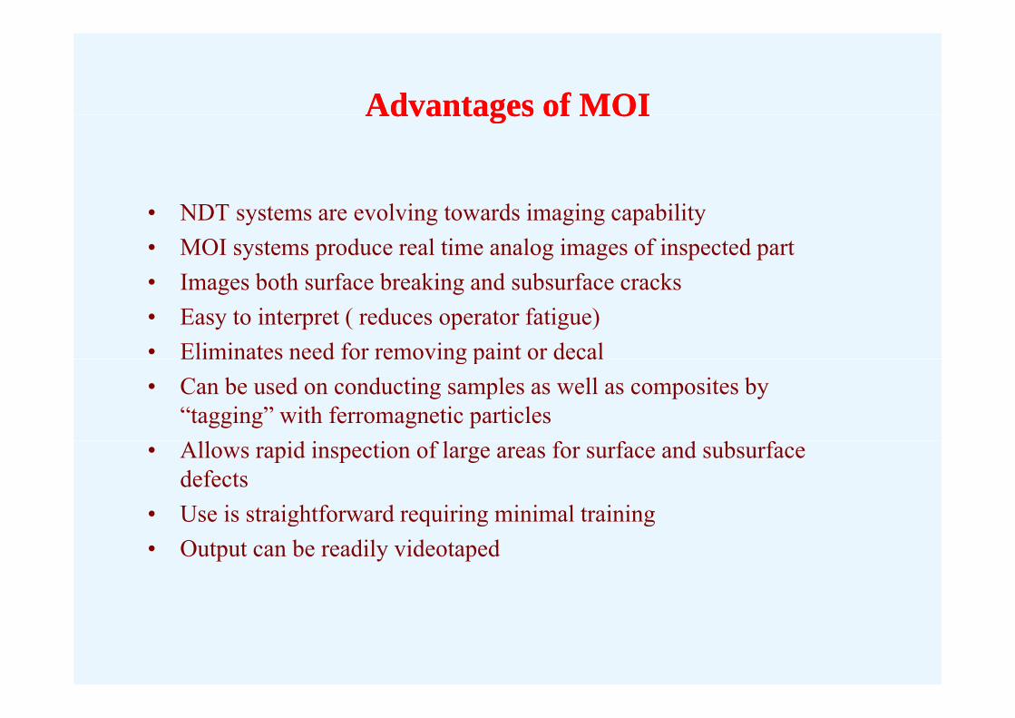
Advantages of MOIAdvantages of MOIAdvantages of MOIAdvantages of MOI
• NDT systems are evolving towards imaging capability• MOI systems produce real time analog images of inspected part
I b th f b ki d b f k• Images both surface breaking and subsurface cracks• Easy to interpret ( reduces operator fatigue)• Eliminates need for removing paint or decalEliminates need for removing paint or decal• Can be used on conducting samples as well as composites by
“tagging” with ferromagnetic particles• Allows rapid inspection of large areas for surface and subsurface
defects• Use is straightforward requiring minimal trainingg q g g• Output can be readily videotaped
Eddy CurrentEddy Current –– GMR SensorsGMR SensorsEddy Current Eddy Current GMR SensorsGMR Sensors
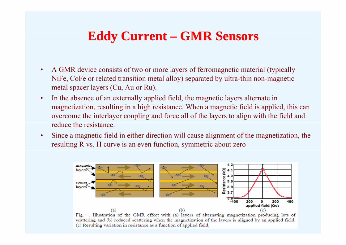
A G d i i f l f f i i l ( i ll• A GMR device consists of two or more layers of ferromagnetic material (typically NiFe, CoFe or related transition metal alloy) separated by ultra-thin non-magnetic metal spacer layers (Cu, Au or Ru).
• In the absence of an externally applied field, the magnetic layers alternate in magnetization, resulting in a high resistance. When a magnetic field is applied, this can overcome the interlayer coupling and force all of the layers to align with the field and
d h ireduce the resistance.• Since a magnetic field in either direction will cause alignment of the magnetization, the
resulting R vs. H curve is an even function, symmetric about zero
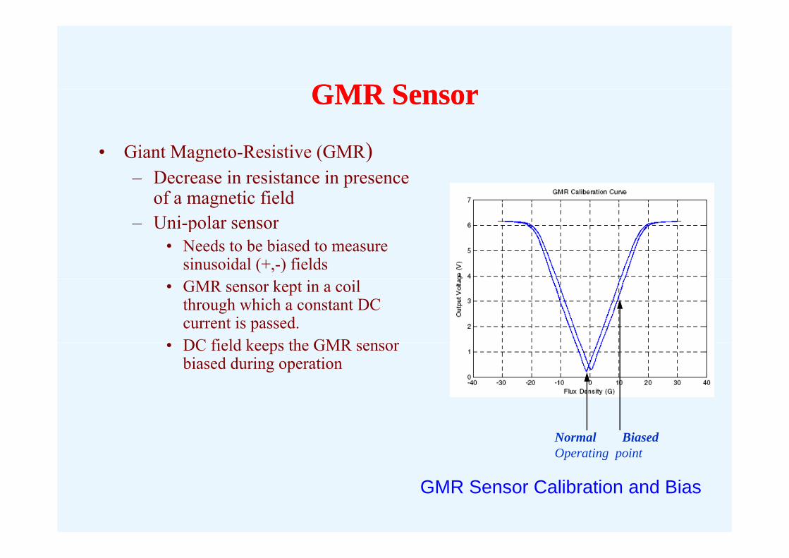
GMR SGMR SGMR SensorGMR Sensor
• Giant Magneto Resistive (GMR)• Giant Magneto-Resistive (GMR)– Decrease in resistance in presence
of a magnetic field i l– Uni-polar sensor
• Needs to be biased to measure sinusoidal (+,-) fields
• GMR sensor kept in a coil through which a constant DC current is passed. DC fi ld k th GMR• DC field keeps the GMR sensor biased during operation
Normal BiasedOperating point
GMR Sensor Calibration and Bias
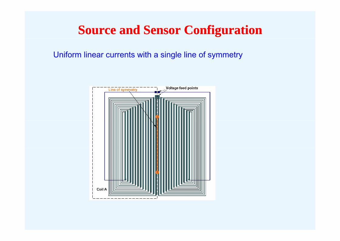
Source and Sensor ConfigurationSource and Sensor Configuration
Uniform linear currents with a single line of symmetry
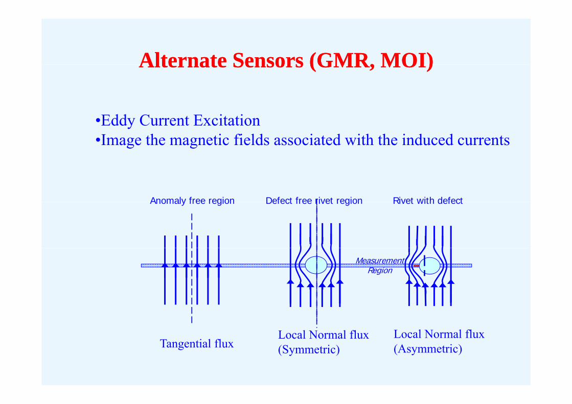
Alternate Sensors (GMR, MOI)Alternate Sensors (GMR, MOI)Alternate Sensors (GMR, MOI)Alternate Sensors (GMR, MOI)
•Eddy Current Excitation•Image the magnetic fields associated with the induced currents
Anomaly free region Defect free rivet region Rivet with defectAnomaly free region Defect free rivet region Rivet with defect
MeasurementRegion
T i l flLocal Normal flux Local Normal flux
Tangential flux (Symmetric) (Asymmetric)
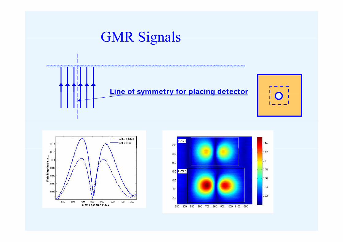
GMR SignalsGMR Signals
Line of symmetry for placing detectorLine of symmetry for placing detector
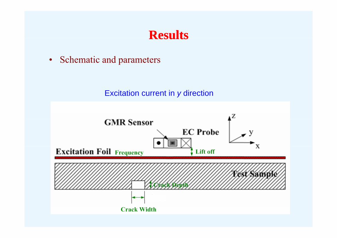
ResultsResultsResultsResults
• Schematic and parameters
Excitation current in y directionExcitation current in y direction
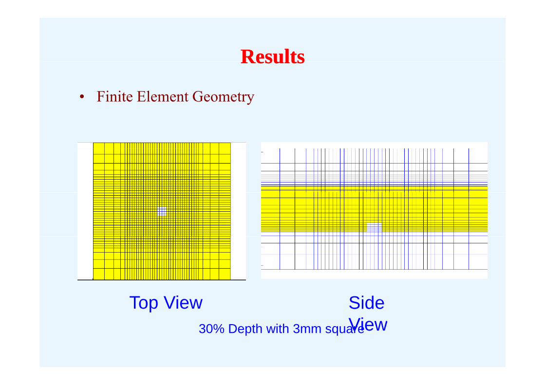
ResultsResultsResultsResults
• Finite Element Geometry
Top View Side View% View30% Depth with 3mm square
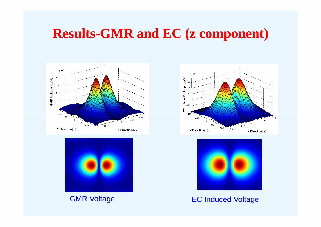
ResultsResults--GMR and EC (z component)GMR and EC (z component)ResultsResults GMR and EC (z component)GMR and EC (z component)
GMR Voltage EC Induced Voltage
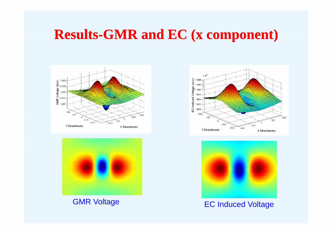
ResultsResults--GMR and EC (x component)GMR and EC (x component)ResultsResults GMR and EC (x component)GMR and EC (x component)
GMR Voltage EC Induced Voltage
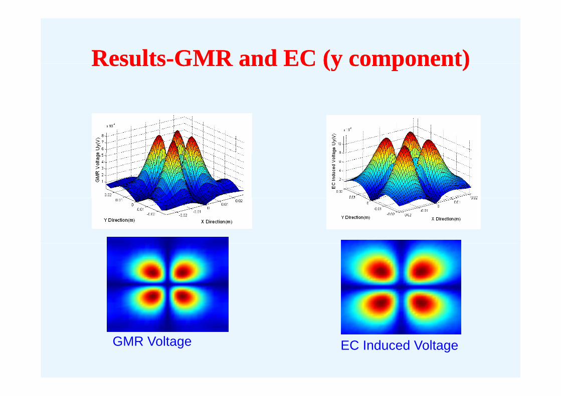
ResultsResults--GMR and EC (y component)GMR and EC (y component)ResultsResults GMR and EC (y component)GMR and EC (y component)
GMR Voltage EC Induced Voltage
Part III Part III -- Eddy Current Inspection ModesEddy Current Inspection Modesy py p
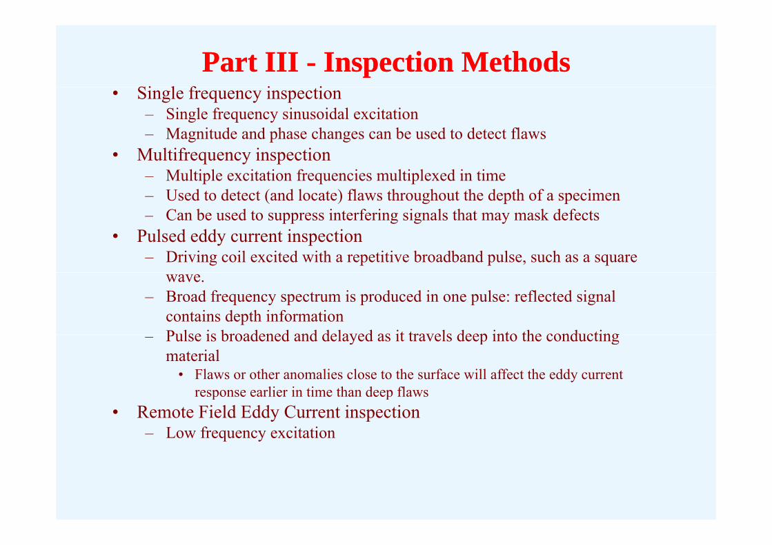
Part III Part III -- Inspection MethodsInspection MethodsSi l f i i• Single frequency inspection– Single frequency sinusoidal excitation– Magnitude and phase changes can be used to detect flaws
M l if i i• Multifrequency inspection– Multiple excitation frequencies multiplexed in time– Used to detect (and locate) flaws throughout the depth of a specimen
C b d t i t f i i l th t k d f t– Can be used to suppress interfering signals that may mask defects• Pulsed eddy current inspection
– Driving coil excited with a repetitive broadband pulse, such as a square wave.
– Broad frequency spectrum is produced in one pulse: reflected signal contains depth information Pulse is broadened and delayed as it travels deep into the conducting– Pulse is broadened and delayed as it travels deep into the conducting material
• Flaws or other anomalies close to the surface will affect the eddy current response earlier in time than deep flawsresponse earlier in time than deep flaws
• Remote Field Eddy Current inspection– Low frequency excitation
Pulsed Eddy CurrentPulsed Eddy Currentyy
1 D i i b il it d ith titi b db d l1. Driving probe coil excited with a repetitive broadband pulse, such as a square wave.
2. Broad frequency spectrum is produced in one pulse:2. Broad frequency spectrum is produced in one pulse: transient/reflected signal contains depth information
3. Pulse is broadened and delayed as it travels deep into the conducting material
• Flaws or other anomalies close to the surface will affect the eddy
li i i h d flcurrent response earlier in time than deep flaws
M i iMotivation
Multilayer aircraft structure needs accurate characterization of
hidden corrosions and cracks
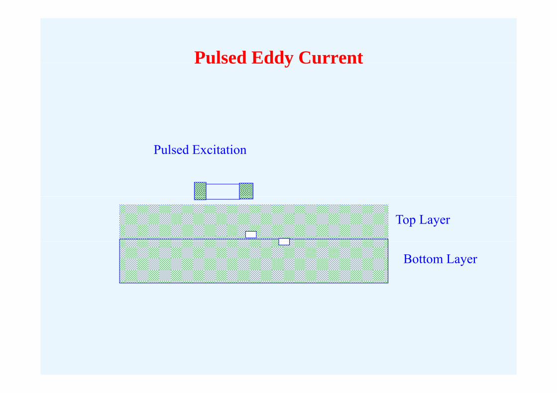
Pulsed Eddy CurrentPulsed Eddy Current
Pulsed ExcitationPulsed Excitation
Top Layer
Bottom Layer
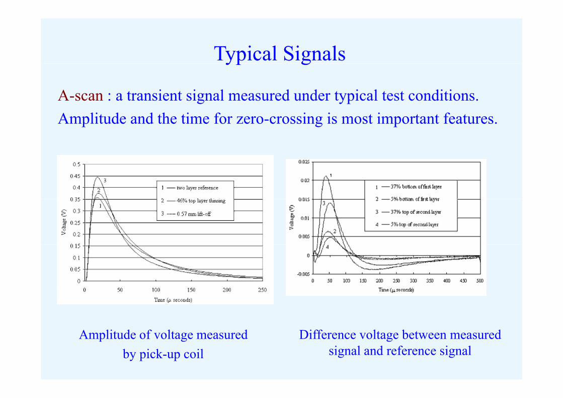
Typical Signalsyp g
A-scan : a transient signal measured under typical test conditions.Amplitude and the time for zero-crossing is most important features.
Amplitude of voltage measured Difference voltage between measuredAmplitude of voltage measured by pick-up coil
Difference voltage between measured signal and reference signal
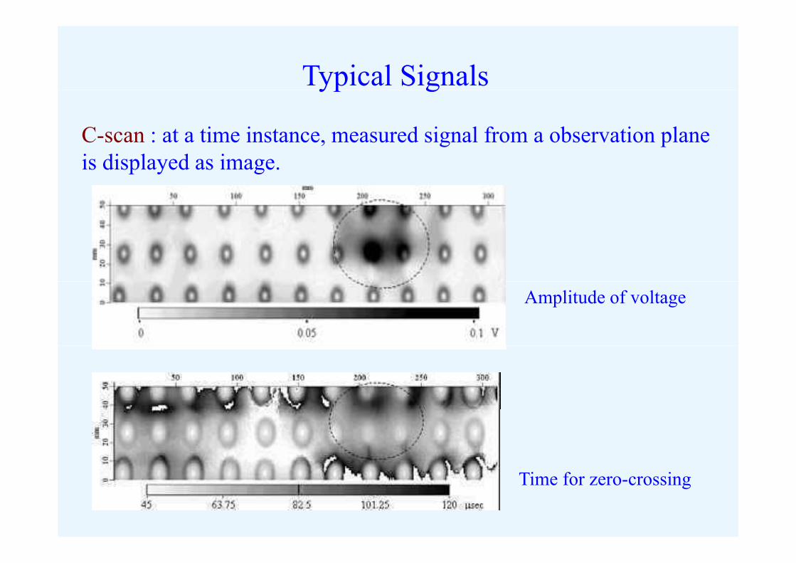
Typical Signalsyp g
C-scan : at a time instance, measured signal from a observation plane i di l d iis displayed as image.
Amplitude of voltage
Ti f iTime for zero-crossing
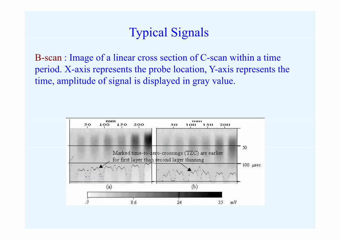
Typical Signalsyp g
B-scan : Image of a linear cross section of C-scan within a time i d i h b l i i hperiod. X-axis represents the probe location, Y-axis represents the
time, amplitude of signal is displayed in gray value.
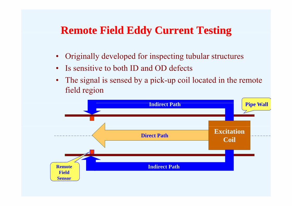
Remote Field Eddy Current TestingRemote Field Eddy Current TestingRemote Field Eddy Current TestingRemote Field Eddy Current Testing
• Originally developed for inspecting tubular structures• Originally developed for inspecting tubular structures• Is sensitive to both ID and OD defects• The signal is sensed by a pick up coil located in the remote
I di t P th Pi W ll
• The signal is sensed by a pick-up coil located in the remote field region
Indirect Path Pipe Wall
ExcitationCoil
Direct Path
Indirect PathRemote FieldField
Sensor
Remote Field Eddy Current TestingRemote Field Eddy Current TestingRemote Field Eddy Current TestingRemote Field Eddy Current Testing
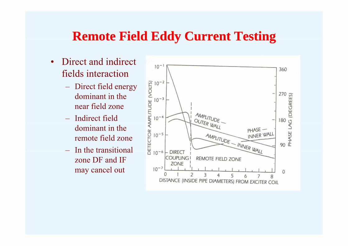
• Direct and indirect fields interaction– Direct field energy
d i t i thdominant in the near field zone
– Indirect field dominant in the remote field zone
– In the transitionalIn the transitional zone DF and IF may cancel out
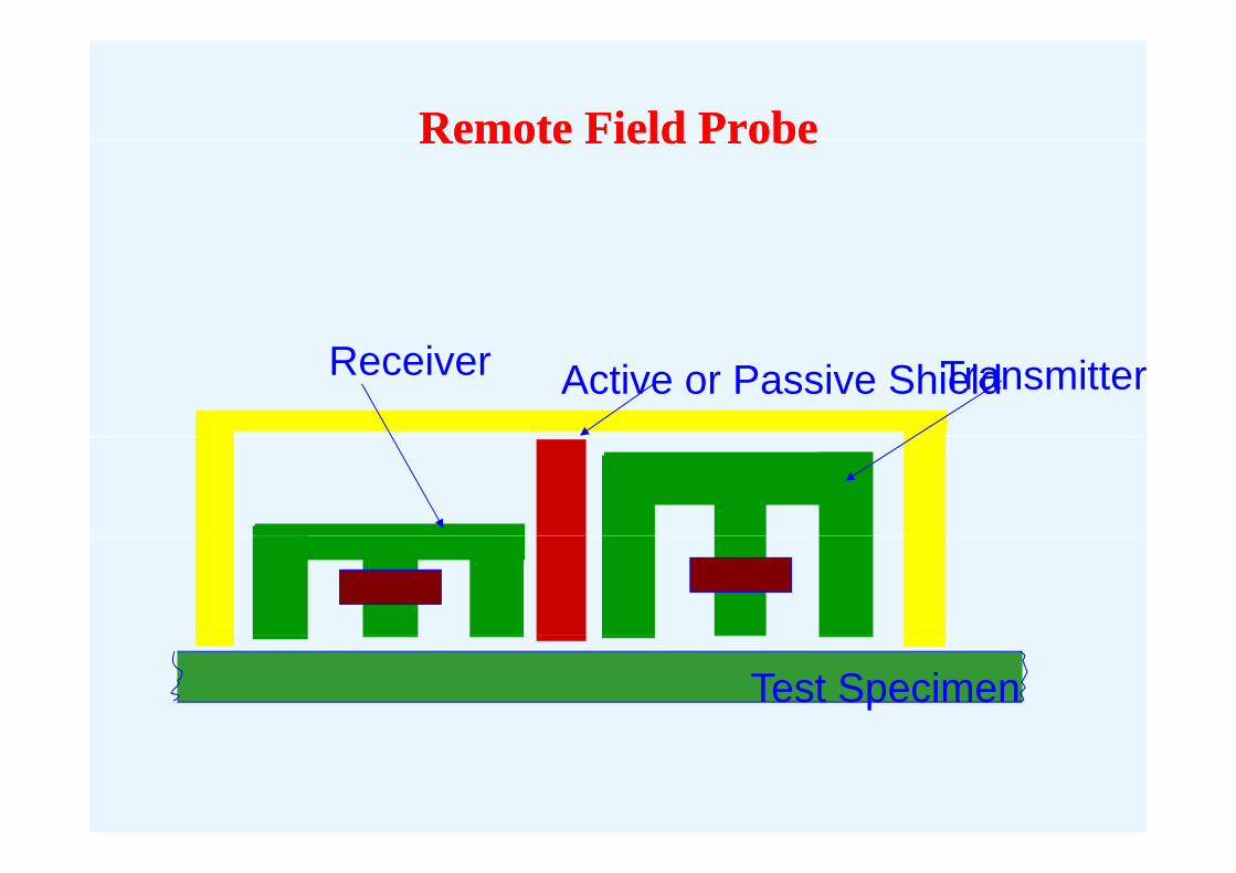
Remote Field ProbeRemote Field ProbeRemote Field ProbeRemote Field Probe
TransmitterReceiver Active or Passive Shield
Test Specimen
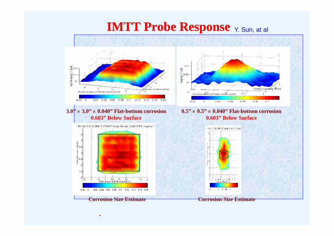
IMTT Probe ResponseIMTT Probe Response Y. Sun, at al
0.5” 0.5” 0.040” Flat-bottom corrosion0 603” Below Surface
3.0” 3.0” 0.040” Flat-bottom corrosion0 603” Below Surface 0.603 Below Surface0.603 Below Surface
C i Si E ti t C i Si E ti tCorrosion Size Estimate Corrosion Size Estimate
.

Part IVPart IV Forward ModelingForward ModelingPart IV Part IV -- Forward Modeling Forward Modeling
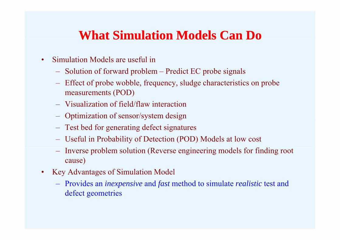
What Simulation Models Can DoWhat Simulation Models Can DoWhat Simulation Models Can DoWhat Simulation Models Can Do
• Simulation Models are useful in– Solution of forward problem – Predict EC probe signals– Effect of probe wobble, frequency, sludge characteristics on probe
measurements (POD)measurements (POD)– Visualization of field/flaw interaction– Optimization of sensor/system design– Test bed for generating defect signatures– Useful in Probability of Detection (POD) Models at low cost– Inverse problem solution (Reverse engineering models for finding root
cause)• Key Advantages of Simulation Modeley dva ages o S u a o ode
– Provides an inexpensive and fast method to simulate realistic test and defect geometries
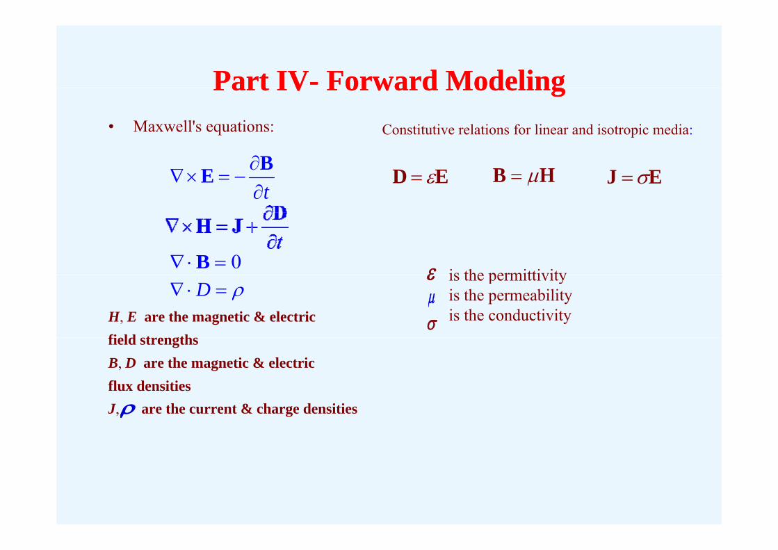
Part IVPart IV-- Forward ModelingForward Modeling• Maxwell's equations:
Part IVPart IV Forward ModelingForward ModelingConstitutive relations for linear and isotropic media:
t
BE ED HB EJ
0 Bis the permittivity
H, E are the magnetic & electric fi ld t th
Dis the permittivityis the permeabilityis the conductivity
field strengthsB, D are the magnetic & electric flux densitiesJ, are the current & charge densities
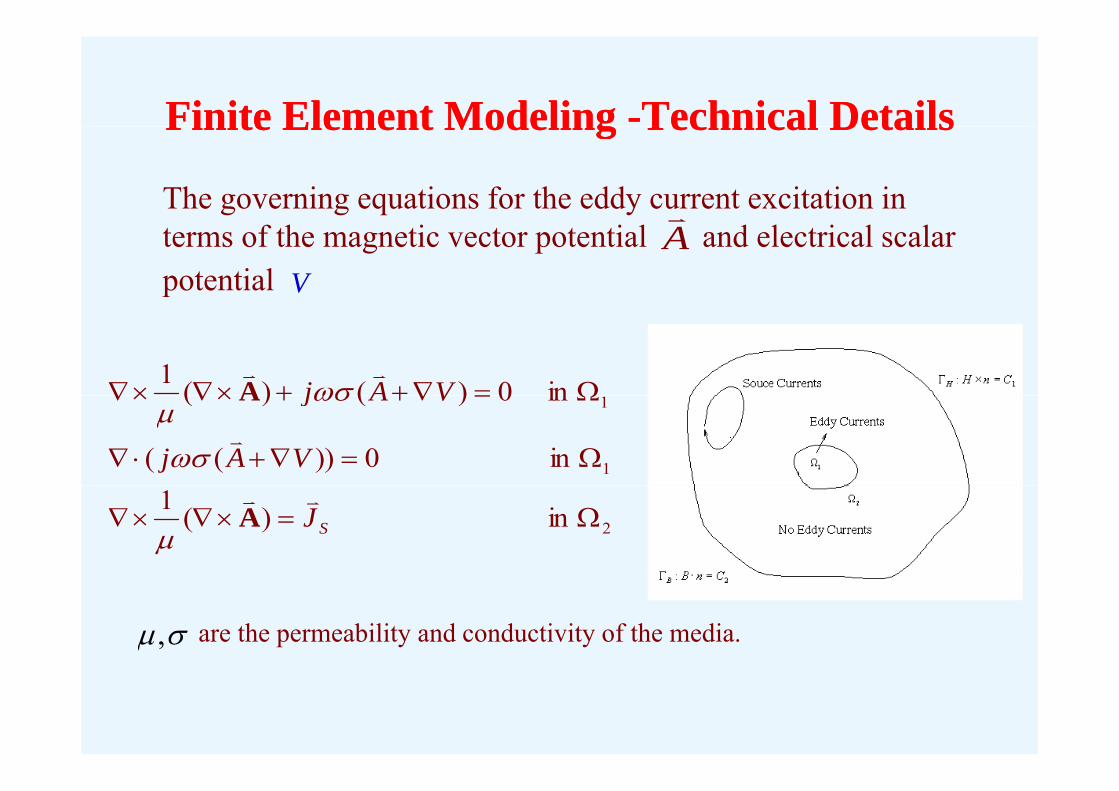
Finite Element ModelingFinite Element Modeling --Technical DetailsTechnical DetailsFinite Element Modeling Finite Element Modeling Technical DetailsTechnical Details
The governing equations for the eddy current excitation in terms of the magnetic vector potential and electrical scalar potential
A
V
in0)()(1 VAj
A
1
1
in 0))((
in 0)()(
VAj
VAj
A
2in )(1 SJ
A
are the permeability and conductivity of the media.,
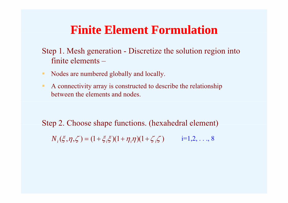
Finite Element FormulationFinite Element FormulationFinite Element FormulationFinite Element FormulationStep 1. Mesh generation - Discretize the solution region into
finite elements – Nodes are numbered globally and locally.
A connectivity array is constructed to describe the relationship between the elements and nodes.
Step 2 Choose shape functions (hexahedral element)Step 2. Choose shape functions. (hexahedral element)
)1)(1)(1(),,( iiiiN i=1,2, . . ., 8
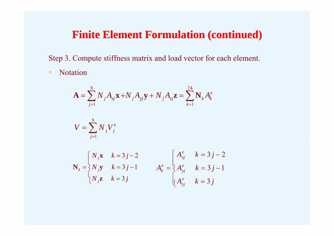
Finite Element Formulation (continued)Finite Element Formulation (continued)Finite Element Formulation (continued)Finite Element Formulation (continued)
Step 3. Compute stiffness matrix and load vector for each element.
Notation
248
ek
kkzjjyjj
jxjj AANANAN
11NzyxA
8
1j
ejjVNV
jkN
jkN
j
j
k 13
23
y
x
N
jkA
jkA
A eyj
exj
ek 13
23
jkN j
j
3 z
jkA
jezj
yjk
3
Finite Element Formulation (continued)Finite Element Formulation (continued)Finite Element Formulation (continued)Finite Element Formulation (continued)
AdV eNNNN }))(1()()1({24
e
VdVNAdVj
AdV
ejji
ejji
jjj
iji
NNN
NNNN
}{}{
}))(()()({
824
1
2421i
eee
ee
dVdSdS Siii
jjj
jjj
JNANAN )1()1(
11
nn
24,,2,1 i
}{}{824
VdVNNAdVNj e
jjkejjk N
0)(11
e
ee
dSVjNk
jj
nA8,,2,1 k
ee QAG 132132e
3232 ][][ ][
Finite Element Formulation (continued)Finite Element Formulation (continued)Finite Element Formulation (continued)Finite Element Formulation (continued)
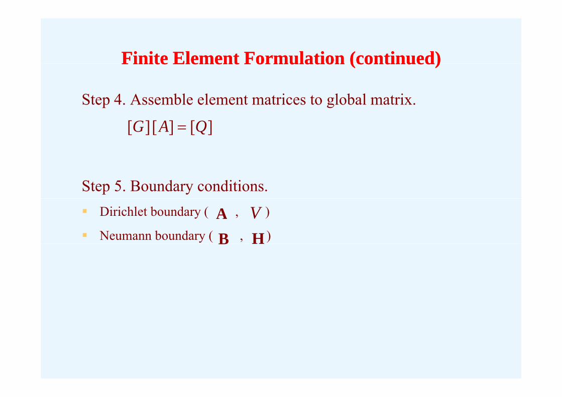
Step 4. Assemble element matrices to global matrix.
][][ ][ QAG
Step 5. Boundary conditions. Dirichlet boundary ( , )
Neumann boundary ( , )A VB HB H
Finite Element Formulation (continued)Finite Element Formulation (continued)Finite Element Formulation (continued)Finite Element Formulation (continued)
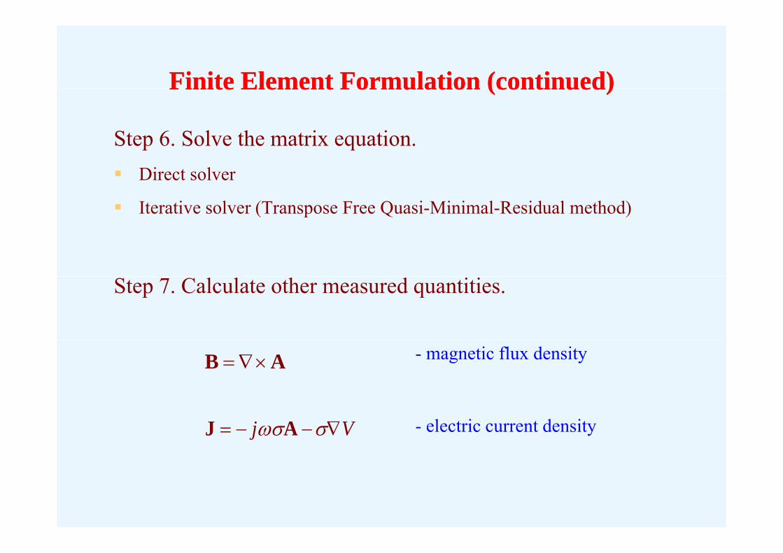
Step 6. Solve the matrix equation. Direct solver
Iterative solver (Transpose Free Quasi-Minimal-Residual method)( p Q )
Step 7. Calculate other measured quantities.
AB - magnetic flux density
Vj AJ - electric current density
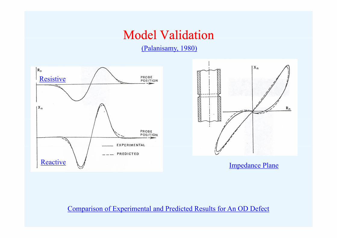
Model ValidationModel ValidationModel ValidationModel Validation(Palanisamy, 1980)
Resistive
Reactive Impedance Plane
Comparison of Experimental and Predicted Results for An OD Defect
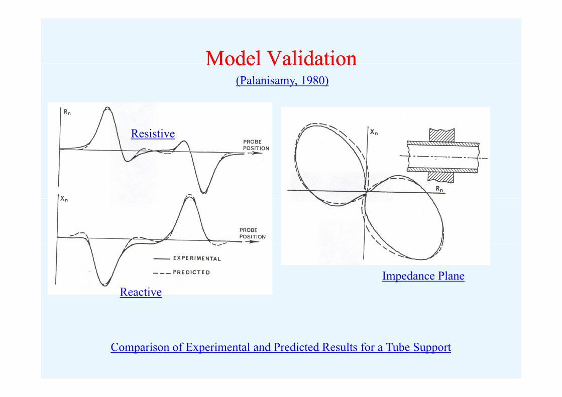
Model ValidationModel ValidationModel ValidationModel Validation(Palanisamy, 1980)
Resistive
R tiImpedance Plane
Reactive
Comparison of Experimental and Predicted Results for a Tube Support
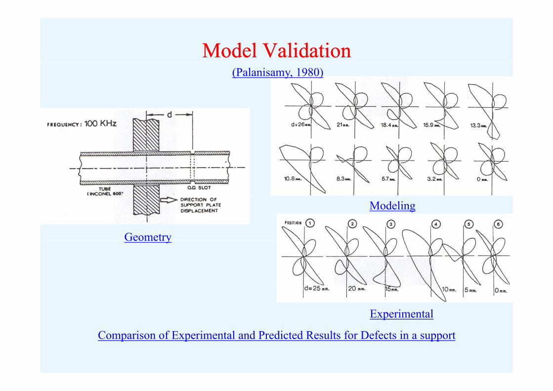
Model ValidationModel Validation(Palanisamy, 1980)
Modeling
GeometryGeometry
Experimental
Comparison of Experimental and Predicted Results for Defects in a support
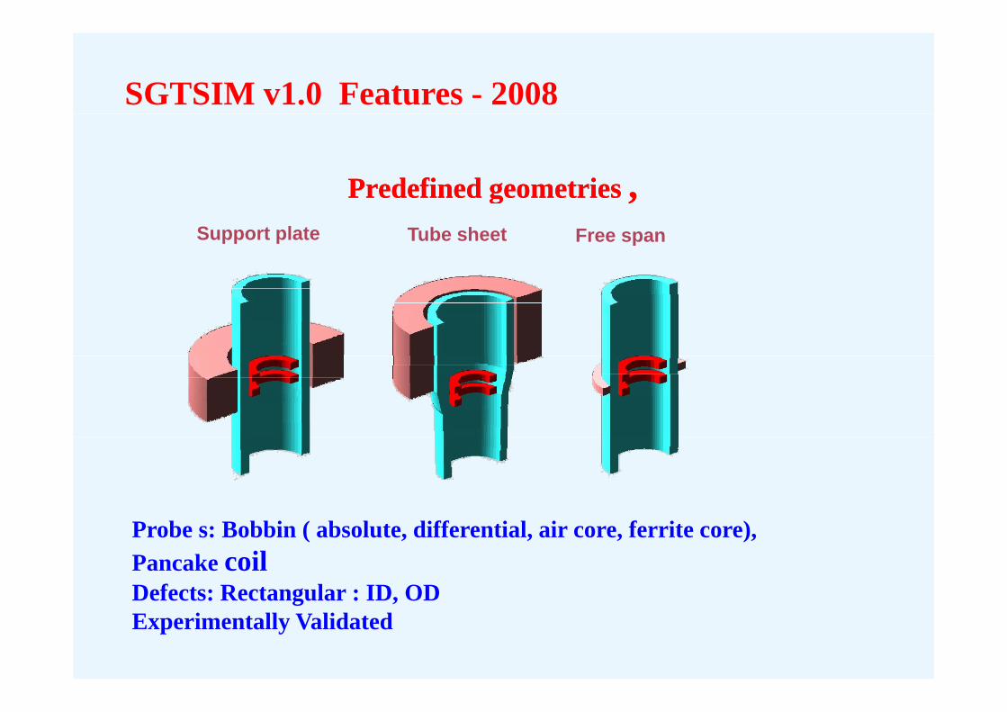
SGTSIM v1.0 Features - 2008
Predefined geometriesPredefined geometries ,,Predefined geometries Predefined geometries , , Support plate Tube sheet Free span
Probe s: Bobbin ( absolute, differential, air core, ferrite core), Pancake coilDefects: Rectangular : ID, ODDefects: Rectangular : ID, ODExperimentally Validated
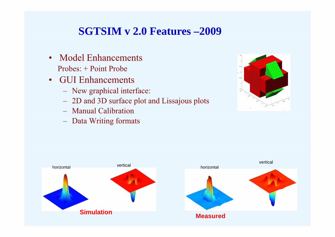
SGTSIM v 2.0 Features –2009
• Model EnhancementsProbes: + Point Probe
• GUI Enhancements– New graphical interface:New graphical interface: – 2D and 3D surface plot and Lissajous plots– Manual Calibration
D W i i f– Data Writing formats
horizontalvertical
horizontal vertical
Simulation Measured
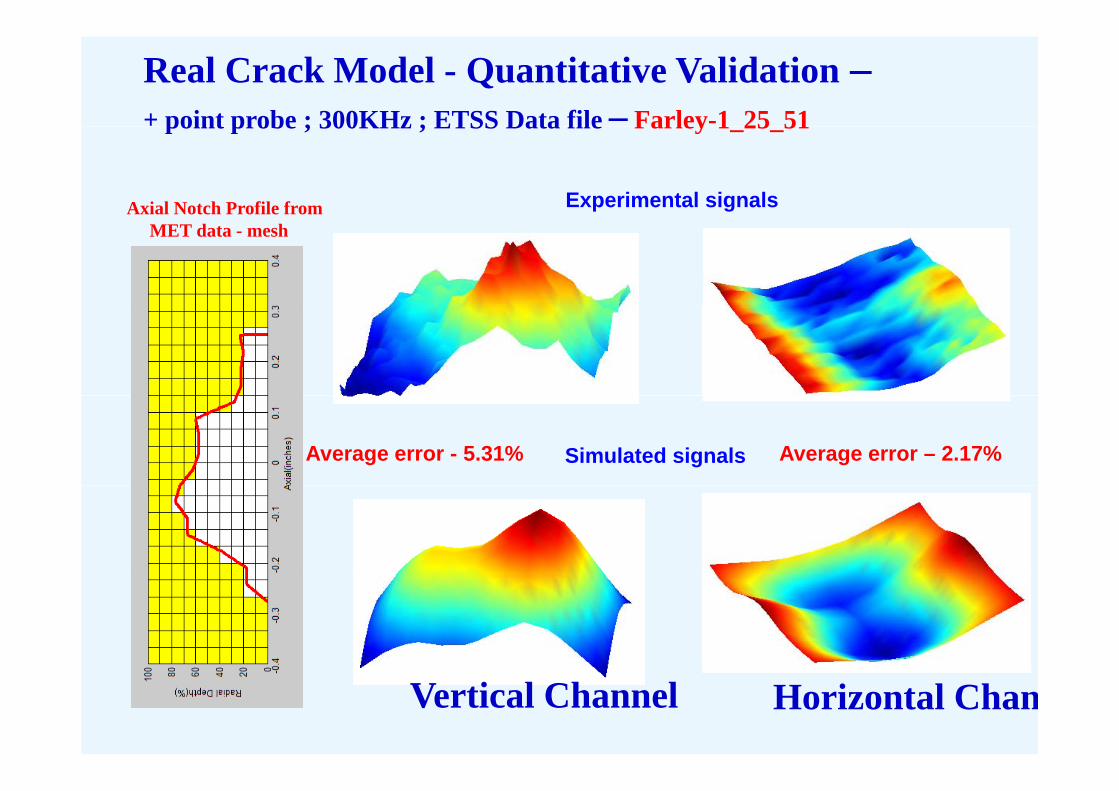
Real Crack Model - Quantitative Validation –+ point probe ; 300KHz ; ETSS Data file – Farley-1 25 51+ point probe ; 300KHz ; ETSS Data file Farley 1_25_51
Experimental signalsAxial Notch Profile from MET data - mesh
Simulated signalsAverage error - 5.31% Average error – 2.17%
Vertical Channel Horizontal Chan
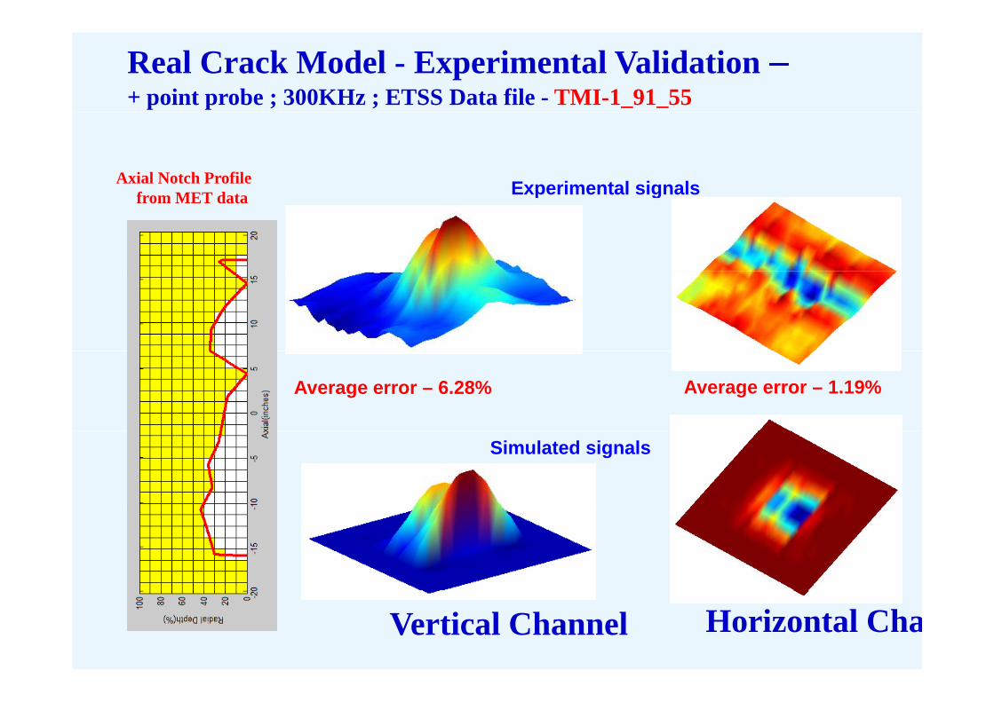
Real Crack Model - Experimental Validation –+ point probe ; 300KHz ; ETSS Data file - TMI-1_91_55
Axial Notch Profile Experimental signalsfrom MET data Experimental signals
Average error – 6.28% Average error – 1.19%
Simulated signals
Vertical Channel Horizontal Cha

Part VPart V Inverse Problems in EC NDEInverse Problems in EC NDEPart V Part V -- Inverse Problems in EC NDEInverse Problems in EC NDE
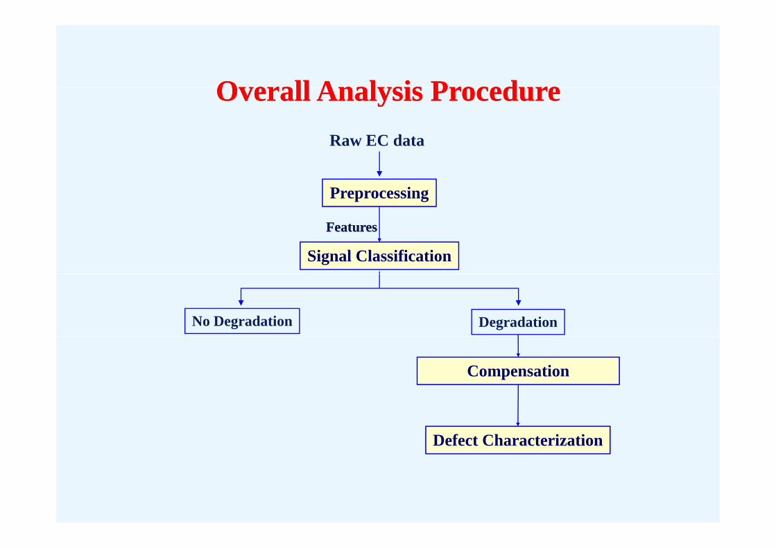
Overall Analysis ProcedureOverall Analysis ProcedureOverall Analysis ProcedureOverall Analysis ProcedureRaw EC data
Preprocessing
Signal Classification
FeaturesFeatures
No Degradation Degradation
Compensation
Defect Characterization
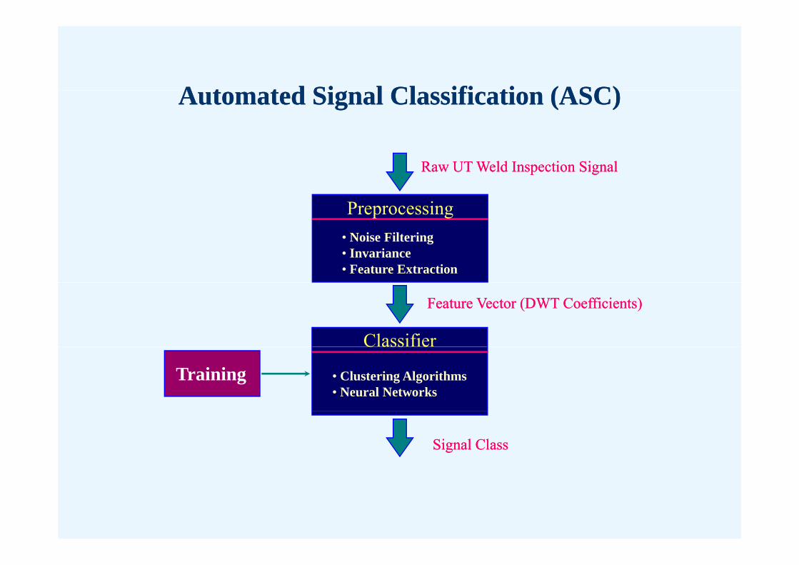
A t t d Si l Cl ifi ti (ASC)A t t d Si l Cl ifi ti (ASC)Automated Signal Classification (ASC)Automated Signal Classification (ASC)
Preprocessing
Raw UT Weld Inspection SignalRaw UT Weld Inspection Signal
• Noise Filtering• Invariance• Feature Extraction
Classifier
Feature Vector (DWT Coefficients)Feature Vector (DWT Coefficients)
C ass e
• Clustering Algorithms• Neural Networks
Training
Signal ClassSignal Class
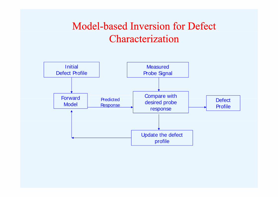
ModelModel--based Inversion for Defect based Inversion for Defect CharacterizationCharacterization
InitialDefect Profile
MeasuredProbe Signal
Forward Compare with P edicted D f tForward
Model
pdesired probe
response
Predicted Response
Defect Profile
Update the defect profilep
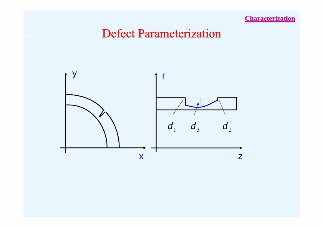
Defect ParameterizationDefect ParameterizationCharacterizationCharacterization
Defect ParameterizationDefect Parameterization
y r
1d 2d3d
x z
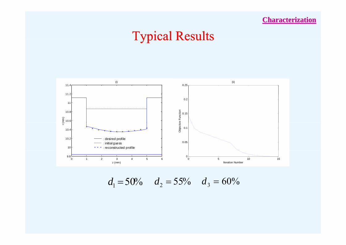
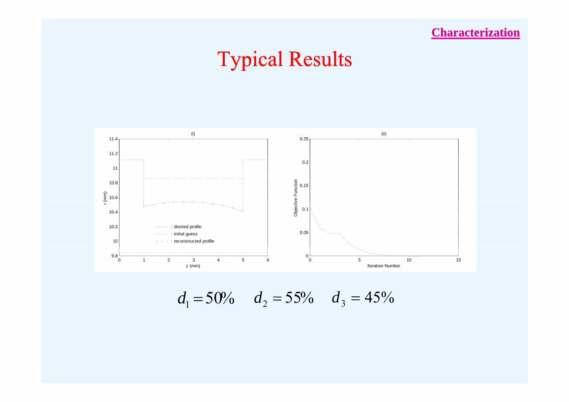
Typical ResultsTypical ResultsCharacterizationCharacterization
Typical ResultsTypical Results
11.2
11.4(i)
11.2
11.4(i) 0.25
(ii)
10.6
10.8
11
11.2
mm
)
10.6
10.8
11
11.2
mm
)
0.15
0.2
e Fu
nctio
n
10
10.2
10.4
r (
: desired profile: initial guess: reconstructed profile10
10.2
10.4
r (
: desired profile: initial guess: reconstructed profile
0.05
0.1
Obj
ectiv
%50d %55d %60d
0 1 2 3 4 5 69.8
z (mm)0 1 2 3 4 5 6
9.8
z (mm)0 5 10 15
0
Iteration Number
%501 d %552 d %603 d
Typical ResultsTypical ResultsCharacterizationCharacterization
Typical ResultsTypical Results
11.2
11.4(i)
0.25(ii)
10.6
10.8
11
(mm
)
0.15
0.2
ve F
unct
ion
10
10.2
10.4
r (
: desired profile: initial guess: reconstructed profile
0.05
0.1
Obj
ectiv
0 1 2 3 4 5 69.8
z (mm)0 5 10 15
0
Iteration Number
%50d %55d %45d%501 d %552 d %453 d
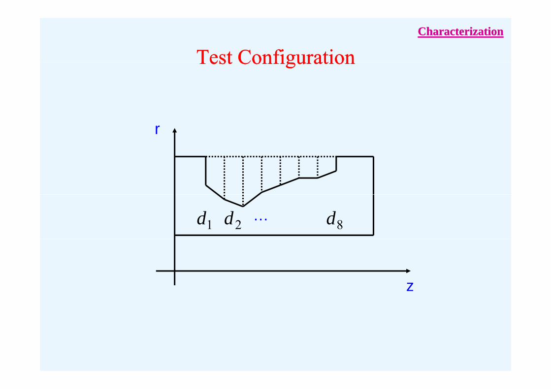
Test ConfigurationTest ConfigurationCharacterizationCharacterization
Test Configuration Test Configuration
r
1d 2d 8d…
zz
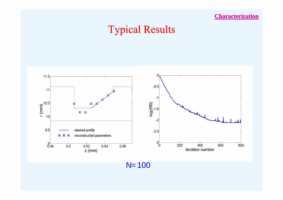
Typical ResultsTypical ResultsCharacterizationCharacterization
Typical ResultsTypical Results
N=100
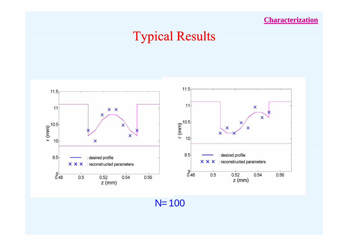
Typical ResultsTypical ResultsCharacterizationCharacterization
Typical ResultsTypical Results
N=100
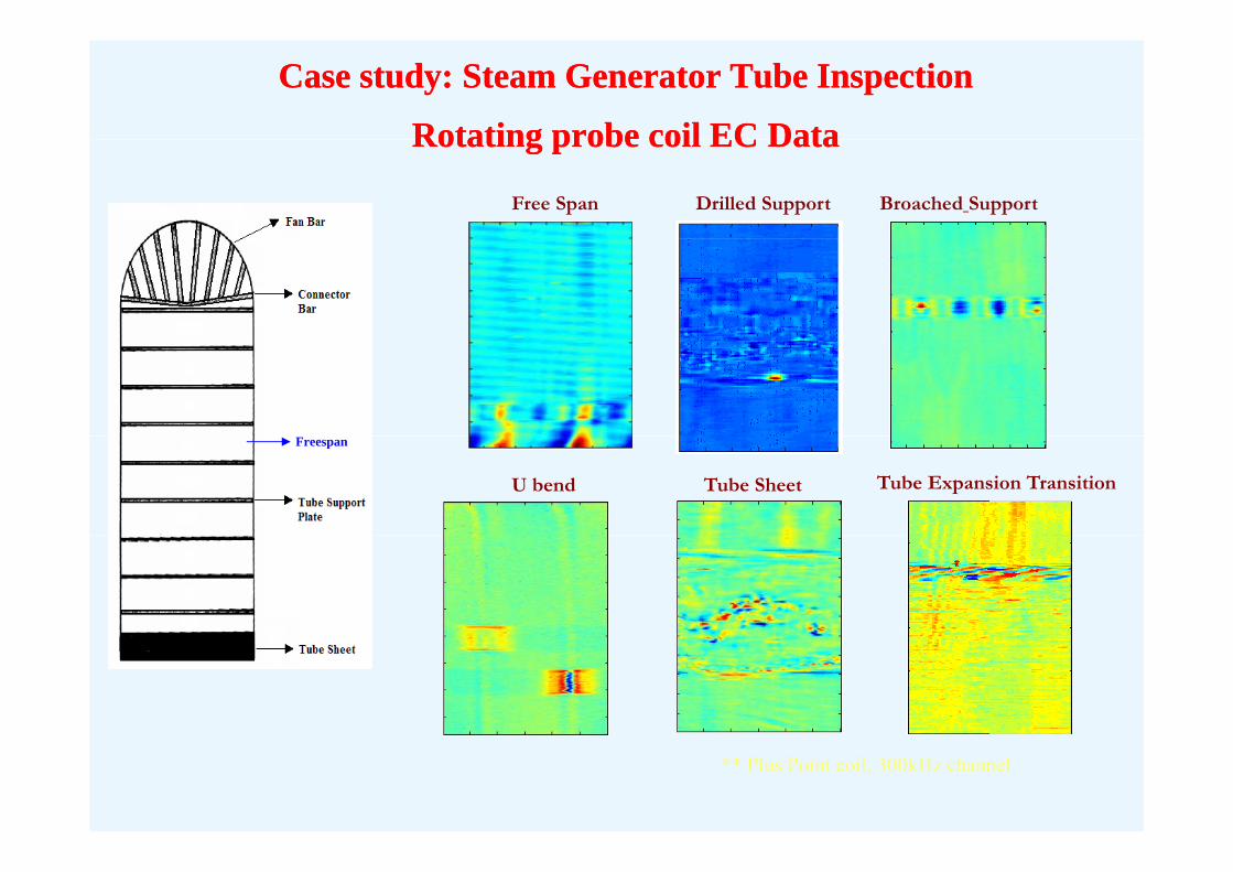
Case study: Steam Generator Tube InspectionCase study: Steam Generator Tube Inspection
RotatingRotating probe coilprobe coil EC DataEC Data
Free Span Drilled Support Broached Support
Rotating Rotating probe coil probe coil EC DataEC Data
U bend Tube Sheet Tube Expansion Transition
Freespan
** Plus Point coil, 300kHz channel
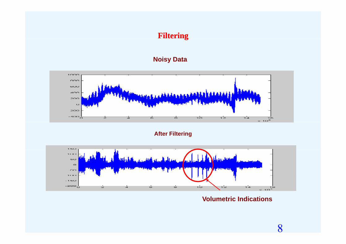
FilteringFilteringgg
Noisy Data
After Filtering
Volumetric Indications
8
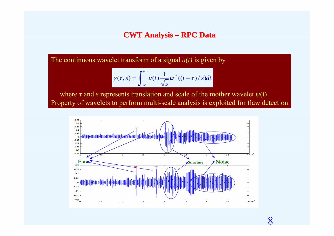
CWT Analysis CWT Analysis –– RPC DataRPC Datayy
The continuous wavelet transform of a signal u(t) is given by
dtsts
tus
)/)((1)(),( *
where τ and s represents translation and scale of the mother wavelet ψ(t)Property of wavelets to perform multi-scale analysis is exploited for flaw detection
Flaw Structure Noise
8
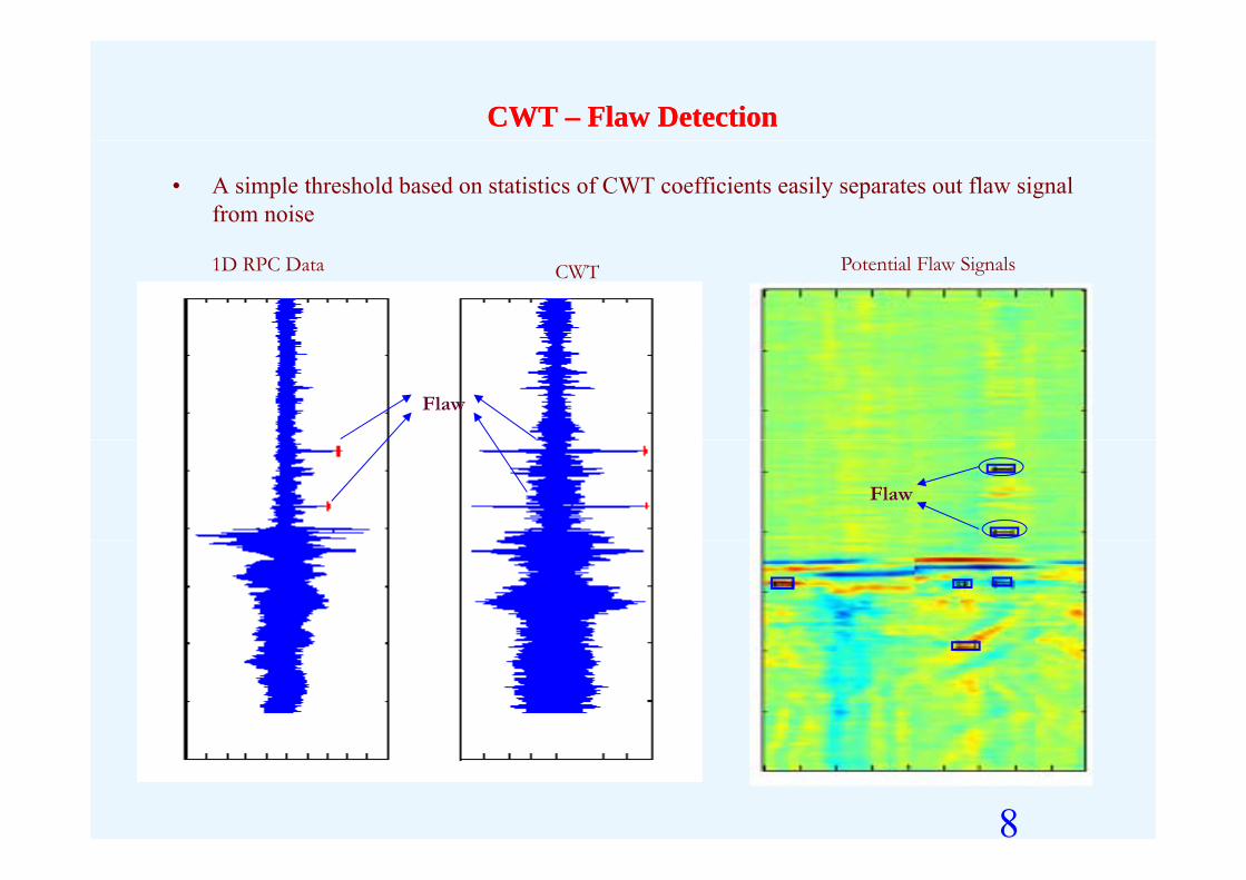
CWT CWT –– Flaw DetectionFlaw Detection
• A simple threshold based on statistics of CWT coefficients easily separates out flaw signal from noise
Potential Flaw Signals1D RPC Data CWT
Flaw
Flaw
8
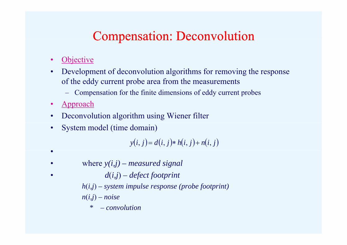
Compensation: DeconvolutionCompensation: DeconvolutionCompensation: DeconvolutionCompensation: Deconvolution
• Objective• Development of deconvolution algorithms for removing the response
of the eddy current probe area from the measurements– Compensation for the finite dimensions of eddy current probesCompensation for the finite dimensions of eddy current probes
• Approach• Deconvolution algorithm using Wiener filter• System model (time domain)
• jinjihjidjiy ,,,,
•• where y(i,j) – measured signal• d(i,j) – defect footprint( ,j) f f p
h(i,j) – system impulse response (probe footprint)n(i,j) – noise
* l ti* – convolution
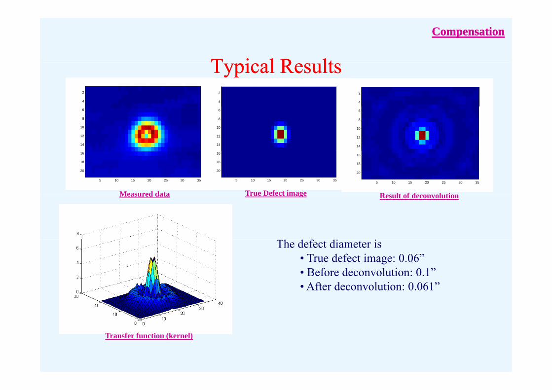
T i l R ltT i l R lt
CompensationCompensation
Typical ResultsTypical Results2
4
2
4
2
4
6
8
10
12
14
6
8
10
12
14
6
8
10
12
14
5 10 15 20 25 30 35
16
18
20
5 10 15 20 25 30 35
16
18
20
5 10 15 20 25 30 35
16
18
20
Measured data True Defect image Result of deconvolutionMeasured data True Defect image Result of deconvolution
The defect diameter is• True defect image: 0.06”• Before deconvolution: 0.1”
Aft d l ti 0 061”• After deconvolution: 0.061”
Transfer function (kernel)
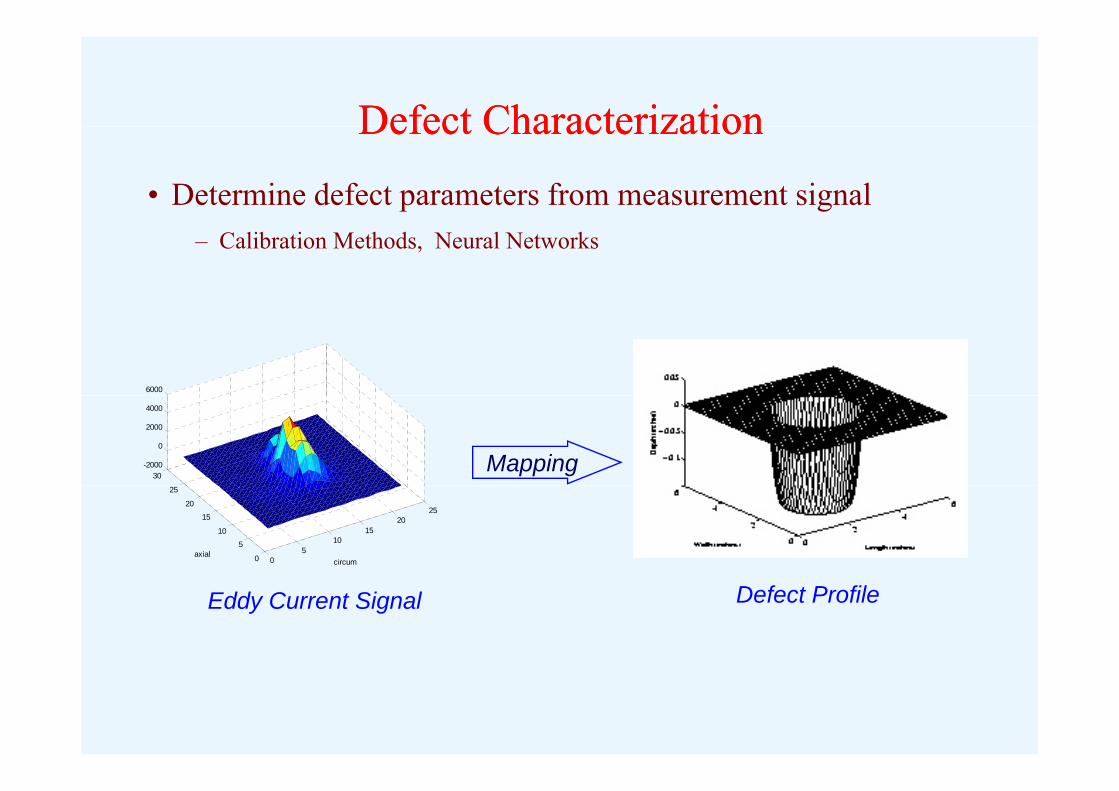
Defect CharacterizationDefect CharacterizationDefect CharacterizationDefect Characterization
• Determine defect parameters from measurement signal– Calibration Methods, Neural Networks
6000
Mapping30
-2000
0
2000
4000
05
1015
2025
0
5
10
15
20
25
circumaxial
Eddy Current Signal Defect Profile
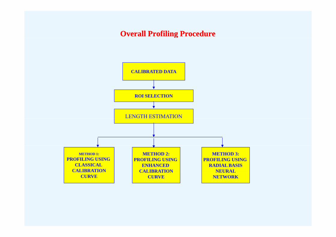
Overall Profiling ProcedureOverall Profiling Proceduregg
CALIBRATED DATA
ROI SELECTION
LENGTH ESTIMATION
METHOD 1:PROFILING USING
CLASSICAL CALIBRATION
METHOD 2:PROFILING USING
ENHANCED CALIBRATION
METHOD 3:PROFILING USING
RADIAL BASISNEURAL
CURVECALIBRATION
CURVENEURAL
NETWORK
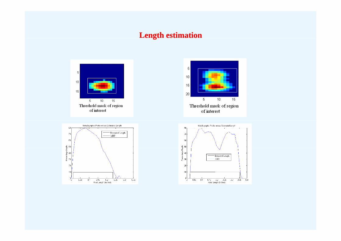
Length estimationLength estimationgg
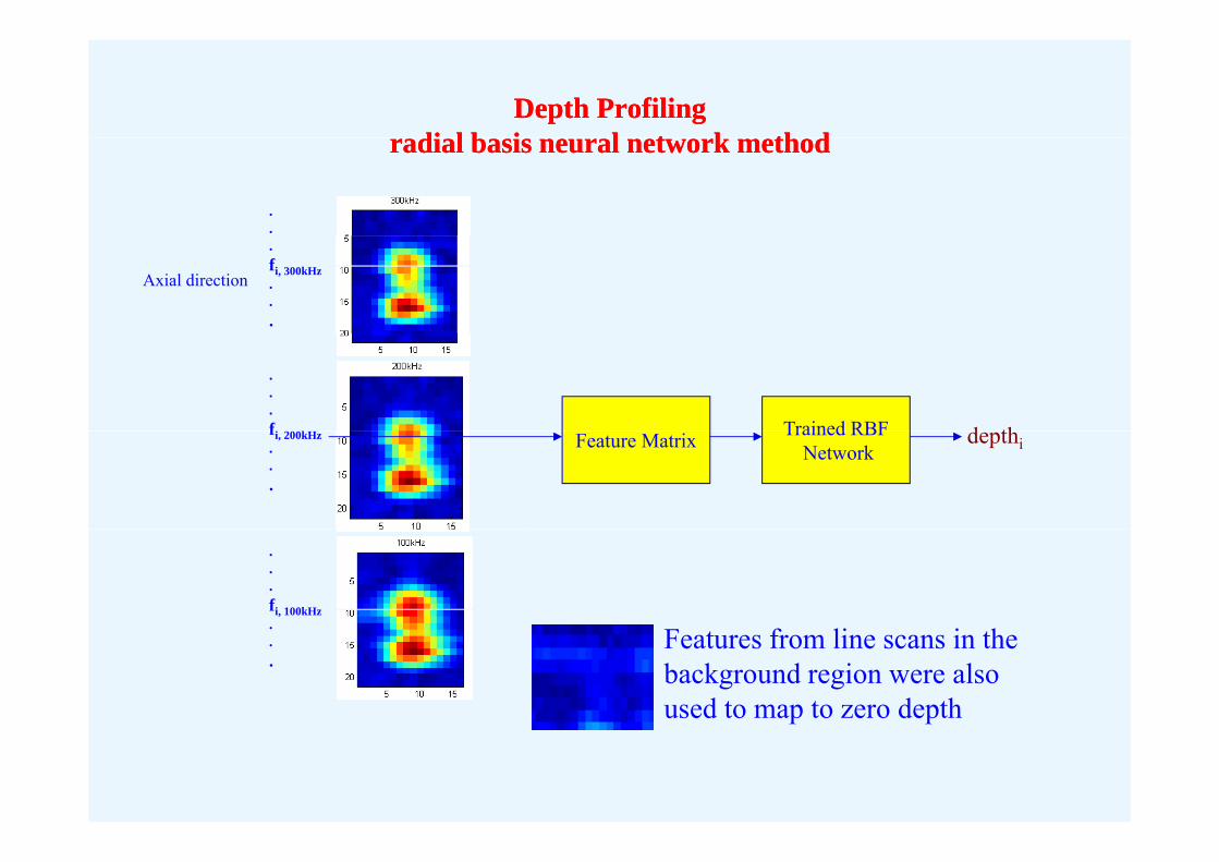
Depth ProfilingDepth Profilingdi l b i l t k th ddi l b i l t k th dradial basis neural network methodradial basis neural network method
.
.
.fi, 300kHz...
Axial direction
.
.
.fi Trained RBF d thfi, 200kHz...
Feature Matrix Trained RBFNetwork
depthi
.
.
.fi, 100kHz....
Features from line scans in the background region were also used to map to zero depth
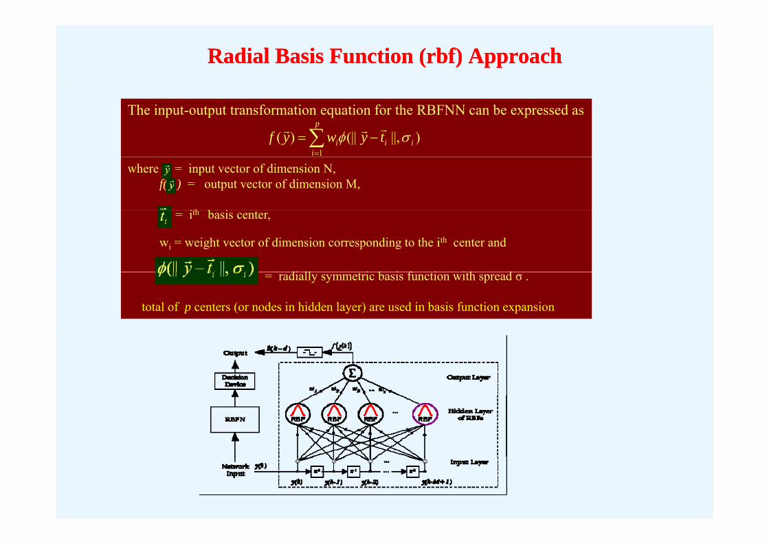
Radial Basis Function (Radial Basis Function (rbfrbf) Approach) Approach
The input-output transformation equation for the RBFNN can be expressed as
p
iii tywyf )||,(||)(
where = input vector of dimension N, f( ) = output vector of dimension M,
ith b i
i 1
= ith basis center,
wi = weight vector of dimension corresponding to the ith center and
di ll i b i f i i h d= radially symmetric basis function with spread σ .
A total of p centers (or nodes in hidden layer) are used in basis function expansion
Feature vectorFeature vectorFeature vectorFeature vector• For 300kHz, 200kHz and 100kHz data, the maximum magnitude and its corresponding phase angle is
computed for each gradation in axial direction of the ROI. • The phase spread which is an additional feature defined as the range for as three phase angles• The phase spread. which is an additional feature, defined as the range for as three phase angles
computed per gradation• Seven features are thus obtained per gradation in axial direction
15
20
2560
90120
Polar plot of raster in 100kHz, 200kHz, 300kHz channel
300,100300200100300200100 ,,, mmmf
5
1030150
180 0
f1f2...
210 330
.
.fN
240270
300
300 kHz200 kHz100 kHz
9
Radial basis neural network methodRadial basis neural network method
12....
N x 7 Feature Matrix
TRAINING MODULELength
Estimation(N Axial scans)
N
Training data MET Result
.
.
.
12
RBF
12...
Test DataFeatureMatrix
.
.
.
.
.
.
LengthEstimation
(M Axial scans)
NETW
M
TEST MODULE
.
.
.M
ORK
Variation of basic rbf algorithm (rbf2)Variation of basic rbf algorithm (rbf2)g ( )g ( )
Three feature vectors corresponding to three spatially contiguous line scans are mapped to depth at center scan
Axial direction fn-1f } depthnNX21
Training data MET Result TRAINING MODULE
fnfn+1
} depthnFeature Matrix
RBF
NET
fn-1fnfn+1
Feature vector Predicted depth at nth scan
WORK
TEST MODULE
Results 1 Results 1 D f t L th & D th filD f t L th & D th filDefect Length & Depth profilesDefect Length & Depth profiles
Max % TW PDA (%) Flaw Length (in)( ) g ( )
Log- Mag 26.00 21.69 0.56
Mag 28.53 22.89 0.52
NN (RBF1) 49.23 32.74 0.52NN (RBF1) 49.23 32.74 0.52
NN2 (RBF2) 56.80 44.52 0.52
MET 60.00 40.97 0.53
RESULTS - profiling
80
90
100
log-mag
40
50
60
70
%TW
log-magmagNNMETNN2
0
10
20
30
0 0.1 0.2 0.3 0.4 0.5 0.6 0.7
Location
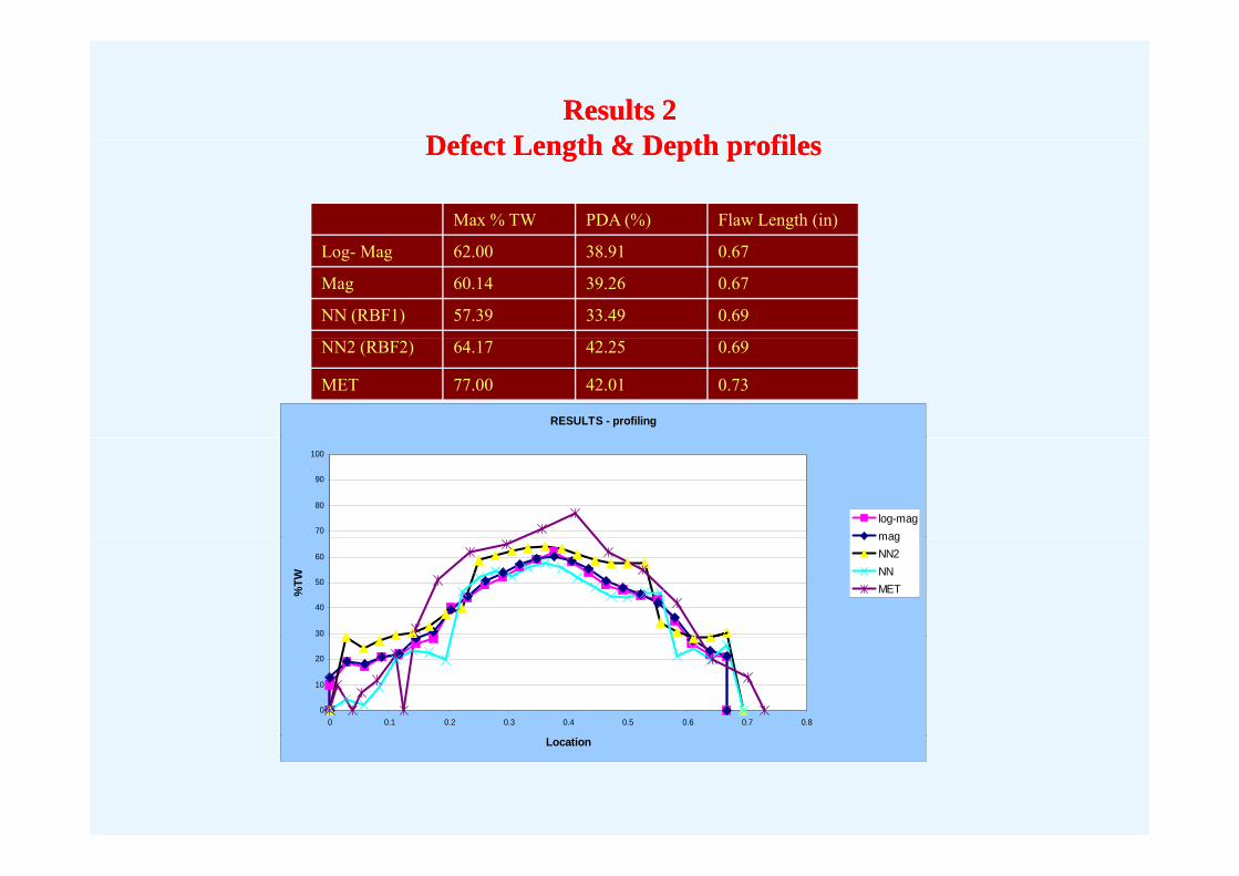
Results 2Results 2D f t L th & D th filD f t L th & D th fil
Max % TW PDA (%) Flaw Length (in)
Defect Length & Depth profilesDefect Length & Depth profiles
Log- Mag 62.00 38.91 0.67
Mag 60.14 39.26 0.67
NN (RBF1) 57.39 33.49 0.69
RESULTS - profiling
NN2 (RBF2) 64.17 42.25 0.69
MET 77.00 42.01 0.73
70
80
90
100
log-magmag
30
40
50
60
%TW
magNN2NNMET
0
10
20
0 0.1 0.2 0.3 0.4 0.5 0.6 0.7 0.8
Location
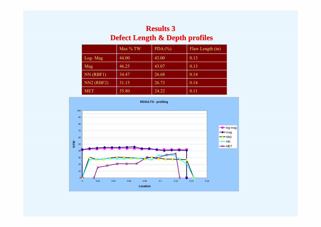
Results 3Results 3D f t L th & D th filD f t L th & D th fil
Max % TW PDA (%) Flaw Length (in)
Log- Mag 44.00 43.00 0.13
Defect Length & Depth profilesDefect Length & Depth profiles
Mag 46.25 43.07 0.13
NN (RBF1) 34.47 26.68 0.14
NN2 (RBF2) 31.15 26.73 0.14
RESULTS - profiling
100
MET 35.80 24.22 0.11
60
70
80
90
log-magmagNN2
20
30
40
50
%TW
NNMET
0
10
0 0.02 0.04 0.06 0.08 0.1 0.12 0.14 0.16
Location
Results 4Results 4D f t L th & D th filD f t L th & D th fil
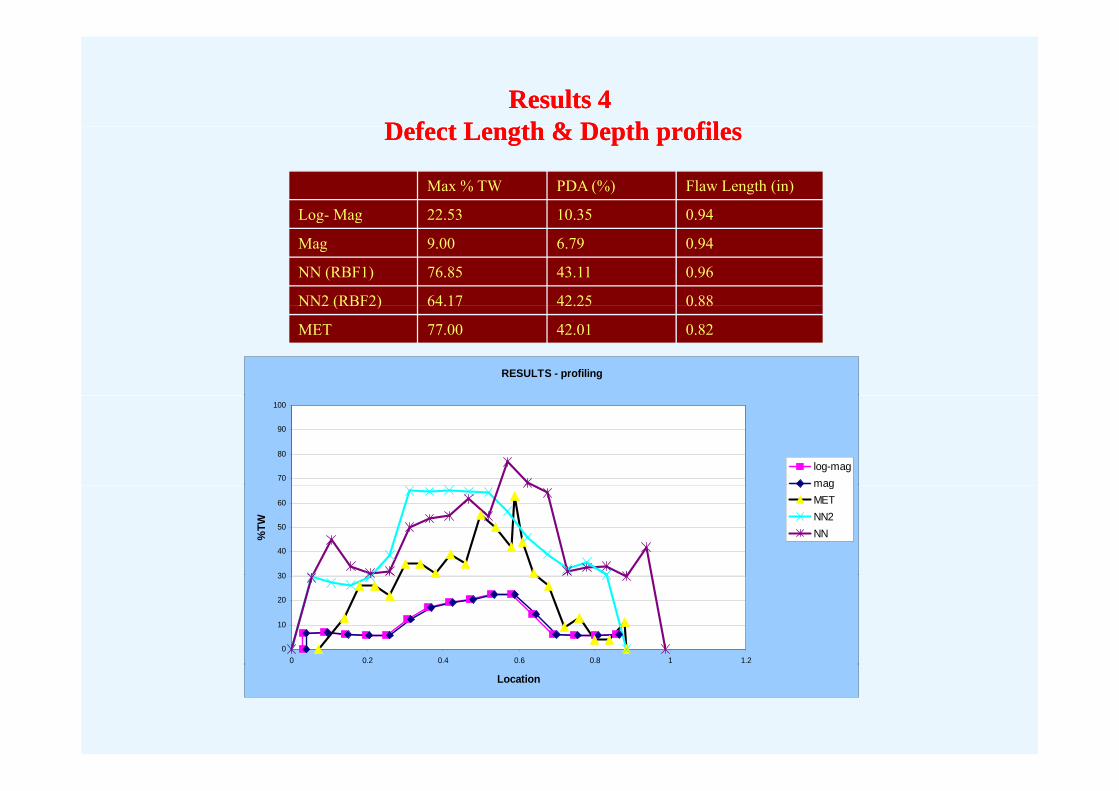
Max % TW PDA (%) Flaw Length (in)
Log- Mag 22 53 10 35 0 94
Defect Length & Depth profilesDefect Length & Depth profiles
Log- Mag 22.53 10.35 0.94
Mag 9.00 6.79 0.94
NN (RBF1) 76.85 43.11 0.96
NN2 (RBF2) 64.17 42.25 0.88NN2 (RBF2) 64.17 42.25 0.88
MET 77.00 42.01 0.82
RESULTS - profiling
70
80
90
100
log-magmag
30
40
50
60
%TW
magMETNN2NN
0
10
20
30
0 0.2 0.4 0.6 0.8 1 1.2
Location
SummarySummarySummarySummary
Edd C t Ph i l P i i lEddy Current - Physical Principles- Transformer Analogy
P b C il t- Probe Coil geometry- Continuous, Pulsed & Remote
it tiexcitation- Simulation models
D t A l i- Data Analysis- Defect Classification
D f t P filiDefect Profiling- Application (SG tube Inspection)

Questions?Questions?Questions?Questions?