EDCQNAUNIT
17
EDC-Unit1 Question&Answer GRIET-ECE G.Surekha Page 1 UNIT-I PN Junction Diode 1. What is an insulator, a semiconductor and a metal? Explain with the help of energy band diagrams. INSULATOR: An insulator is a material that offers a very low level of conductivity under Pressure from an applied voltage source. In this material Forbidden energy gap is large (E G 6e.V).So, electron can not acquire enough energy and hence conduction is not possible. Ex: Diamond is a perfect insulator. SEMI CONDUCTOR: A semiconductor, is a material that has a conductivity level somewhere in between the extremes of an insulator and a conductor. Energy gap is only about 1ev. Ex: Germanium, Silicon(Energy gap of Germanium is about 0.785 ev and for silicon it is 1.21ev). CONDUCTOR: Conductor is a material that will support a generous flow of charge when a voltage source of limited magnitude is applied across its terminals. There is no energy gap in conductors. Conduction band and valence band are overlapped. Ex:Copper,Aluminium. 2. What is meant by doping? Explain about intrinsic & extrinsic semiconductors, N-type material & P-type material. DOPING: Adding impurities in a semiconductor is called Doping. Pure semiconductor is called Intrinsic semiconductor. Semiconductor with impurities added are called extrinsic semiconductor. www.jntuworld.com www.jntuworld.com
-
Upload
ashok94405251218258 -
Category
Documents
-
view
22 -
download
0
description
edcq free notes
Transcript of EDCQNAUNIT
EDC-Unit1 Question&Answer
GRIET-ECE G.Surekha Page 1
UNIT-I PN Junction Diode
1. What is an insulator, a semiconductor and a metal? Explain with the help of energy band
diagrams.
INSULATOR:
An insulator is a material that offers a very low level of conductivity under Pressure from an
applied voltage source. In this material Forbidden energy gap is large (EG 6e.V).So, electron
can not acquire enough energy and hence conduction is not possible. Ex: Diamond is a perfect
insulator.
SEMI CONDUCTOR:
A semiconductor, is a material that has a conductivity level somewhere in between the extremes
of an insulator and a conductor. Energy gap is only about 1ev. Ex: Germanium, Silicon(Energy
gap of Germanium is about 0.785 ev and for silicon it is 1.21ev).
CONDUCTOR:
Conductor is a material that will support a generous flow of charge when a voltage source of
limited magnitude is applied across its terminals. There is no energy gap in conductors.
Conduction band and valence band are overlapped. Ex:Copper,Aluminium.
2. What is meant by doping? Explain about intrinsic & extrinsic semiconductors, N-type material
& P-type material.
DOPING: Adding impurities in a semiconductor is called Doping.
Pure semiconductor is called Intrinsic semiconductor. Semiconductor with impurities added are
called extrinsic semiconductor.
www.jntuworld.com
www.jntuworld.com

EDC-Unit1 Question&Answer
GRIET-ECE G.Surekha Page 2
EXTRINSIC MATERIALS—
n- and p-type
The characteristics of semiconductor materials can be altered significantly by the addition of
certain impurity atoms into the relatively pure semiconductor material. These impurities,
although only added to perhaps 1 part in 10 million, can alter the band structure sufficiently to
totally change the electrical properties of the material. A semiconductor material that has been
subjected to the doping process is called an extrinsic material. There are two extrinsic materials
of immeasurable importance to semiconductor device fabrication: n-type and p-type.
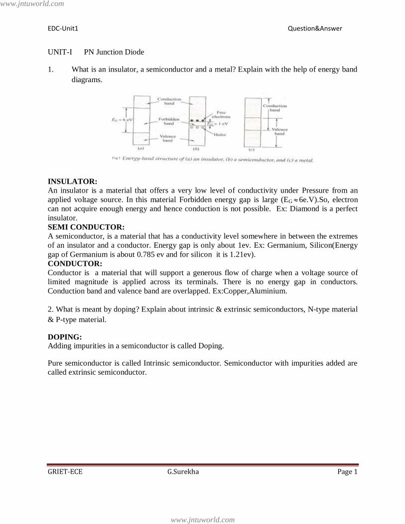
n-Type Material
Both the n- and p-type materials are formed by adding a predetermined number of impurity
atoms into a germanium or silicon base. The n-type is created by introducing those impurity
elements that have five valence electrons (pentavalent), such as antimony, arsenic, and
phosphorus. The effect of such impurity elements is indicated in
Figure.1 Antimony impurity in n-type material
Fig.1 (using antimony as the impurity in a silicon base). Note that the four covalent bonds are
still present. There is, however, an additional fifth electron due to the impurity atom, which is
unassociated with any particular covalent bond. This remaining electron, loosely bound to its
www.jntuworld.com
www.jntuworld.com
EDC-Unit1 Question&Answer
GRIET-ECE G.Surekha Page 3
parent (antimony) atom, is relatively free to move within the newly formed n-type material.
Since the inserted impurity atom has donated a relatively ―free‖ electron to the structure:
Diffused impurities with five valence electrons are called donor atoms. The effect of this doping
process on the relative conductivity can best be described through the use of the energy-band
diagram of Fig. 1.1.
Figure 1.1 Effect of donor impurities on the energy band structure.
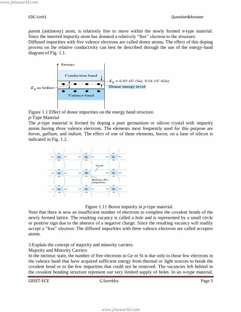
p-Type Material
The p-type material is formed by doping a pure germanium or silicon crystal with impurity
atoms having three valence electrons. The elements most frequently used for this purpose are
boron, gallium, and indium. The effect of one of these elements, boron, on a base of silicon is
indicated in Fig. 1.2.
Figure 1.11 Boron impurity in p-type material.
Note that there is now an insufficient number of electrons to complete the covalent bonds of the
newly formed lattice. The resulting vacancy is called a hole and is represented by a small circle
or positive sign due to the absence of a negative charge. Since the resulting vacancy will readily
accept a ―free‖ electron: The diffused impurities with three valence electrons are called acceptor
atoms.
3.Explain the concept of majority and minority carriers.
Majority and Minority Carriers
In the intrinsic state, the number of free electrons in Ge or Si is due only to those few electrons in
the valence band that have acquired sufficient energy from thermal or light sources to break the
covalent bond or to the few impurities that could not be removed. The vacancies left behind in
the covalent bonding structure represent our very limited supply of holes. In an n-type material,
www.jntuworld.com
www.jntuworld.com

EDC-Unit1 Question&Answer
GRIET-ECE G.Surekha Page 4
the number of holes has not changed significantly from this intrinsic level. The net result,
therefore, is that the number of electrons far outweighs the number of holes. For this reason:
In an n-type material (Fig. 1.13a) the electron is called the majority carrier and the hole the
minority carrier.
For the p-type material the number of holes far outweighs the number of electrons, as shown in
Fig. 1.13b. Therefore: In a p-type material the hole is the majority carrier and the electron is the
minority carrier. When the fifth electron of a donor atom leaves the parent atom, the atom
remaining acquires a net positive charge: hence the positive sign in the donor-ion representation.
For similar reasons, the negative sign appears in the acceptor ion.
Figure 1.13 (a) n-type material; (b) p-type material.
Fermi Level in N & P type materials is shown in below Fig:
In N type material Fermi level is just below the conduction band. In P type material Fermi level
is just above the valence band.
4. Explain PN diode characteristics in forward bias and reverse bias regions.
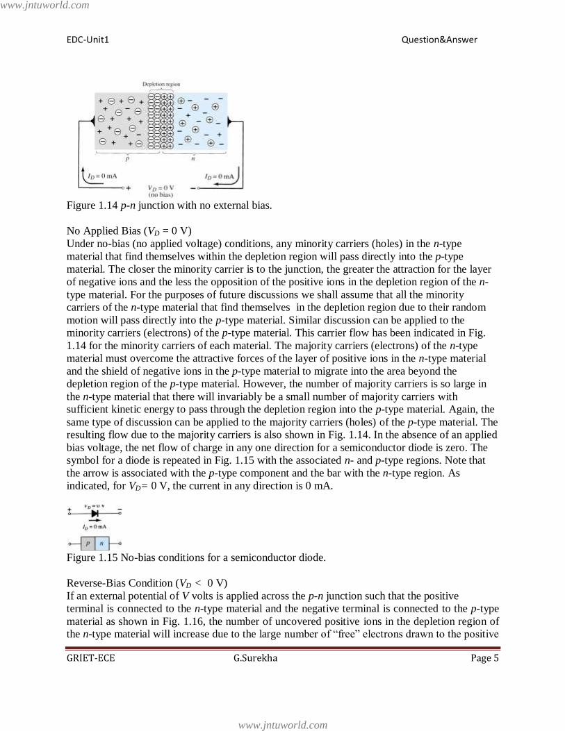
The semiconductor diode is formed by simply bringing these materials together (constructed
from the same base—Ge or Si), as shown in Fig. 1.14. At the instant the two materials are
―joined‖ the electrons and holes in the region of the junction will combine, resulting in a lack of
carriers in the region near the junction. This region of uncovered positive and negative ions is
called the depletion region due to the depletion of carriers in this region. Since the diode is a
two-terminal device, the application of a voltage across its terminals leaves three possibilities: no
bias (VD = 0 V), forward bias (VD >0 V), and reverse bias (VD< 0 V).
www.jntuworld.com
www.jntuworld.com
EDC-Unit1 Question&Answer
GRIET-ECE G.Surekha Page 5
Figure 1.14 p-n junction with no external bias.
No Applied Bias (VD = 0 V)
Under no-bias (no applied voltage) conditions, any minority carriers (holes) in the n-type
material that find themselves within the depletion region will pass directly into the p-type
material. The closer the minority carrier is to the junction, the greater the attraction for the layer
of negative ions and the less the opposition of the positive ions in the depletion region of the n-
type material. For the purposes of future discussions we shall assume that all the minority
carriers of the n-type material that find themselves in the depletion region due to their random
motion will pass directly into the p-type material. Similar discussion can be applied to the
minority carriers (electrons) of the p-type material. This carrier flow has been indicated in Fig.
1.14 for the minority carriers of each material. The majority carriers (electrons) of the n-type
material must overcome the attractive forces of the layer of positive ions in the n-type material
and the shield of negative ions in the p-type material to migrate into the area beyond the
depletion region of the p-type material. However, the number of majority carriers is so large in
the n-type material that there will invariably be a small number of majority carriers with
sufficient kinetic energy to pass through the depletion region into the p-type material. Again, the
same type of discussion can be applied to the majority carriers (holes) of the p-type material. The
resulting flow due to the majority carriers is also shown in Fig. 1.14. In the absence of an applied
bias voltage, the net flow of charge in any one direction for a semiconductor diode is zero. The
symbol for a diode is repeated in Fig. 1.15 with the associated n- and p-type regions. Note that
the arrow is associated with the p-type component and the bar with the n-type region. As
indicated, for VD= 0 V, the current in any direction is 0 mA.
Figure 1.15 No-bias conditions for a semiconductor diode.
Reverse-Bias Condition (VD < 0 V)
If an external potential of V volts is applied across the p-n junction such that the positive
terminal is connected to the n-type material and the negative terminal is connected to the p-type
material as shown in Fig. 1.16, the number of uncovered positive ions in the depletion region of
the n-type material will increase due to the large number of ―free‖ electrons drawn to the positive
www.jntuworld.com
www.jntuworld.com

EDC-Unit1 Question&Answer
GRIET-ECE G.Surekha Page 6
potential of the applied voltage. For similar reasons, the number of uncovered negative ions will
increase in the p-type material. The net effect, therefore, is a widening of the depletion region.
This widening of the depletion region will establish too great a barrier for the majority carriers to
overcome, effectively reducing the majority carrier flow to zero as shown in Fig. 1.16.
Figure 1.16 Reverse-biased p-n junction.
The number of minority carriers, however, that find themselves entering the depletion region will
not change, resulting in minority-carrier flow vectors of the same magnitude indicated in Fig.
1.14 with no applied voltage the current that exists under reverse-bias conditions is called the
reverse saturation current and is represented by Io.
Forward-Bias Condition (VD > 0 V)
A forward-bias or ―on‖ condition is established by applying the positive potential to the p-type
material and the negative potential to the n-type material as shown in Fig. 1.18. A semiconductor
diode is forward-biased when the association p-type and positive and n-type and negative has
been established.
Figure 1.18 Forward-biased p-n junction
The application of a forward-bias potential VD will ―pressure‖ electrons in the n-type material
and holes in the p-type material to recombine with the ions near the boundary and reduce the
width of the depletion region as shown in Fig. 1.18. The resulting minority-carrier flow of
electrons from the p-type material to the n-type material (and of holes from the n-type material to
the p-type material) has not changed in magnitude (since the conduction level is controlled
primarily by the limited number of impurities in the material), but the reduction in the width of
the depletion region has resulted in a heavy majority flow across the junction. An electron of the
n-type material now ―sees‖ a reduced barrier at the junction due to the reduced depletion region
and a strong attraction for the positive potential applied to the p-type material. As the applied
bias increases in magnitude the depletion region will continue to decrease in width until a flood
www.jntuworld.com
www.jntuworld.com
EDC-Unit1 Question&Answer
GRIET-ECE G.Surekha Page 7
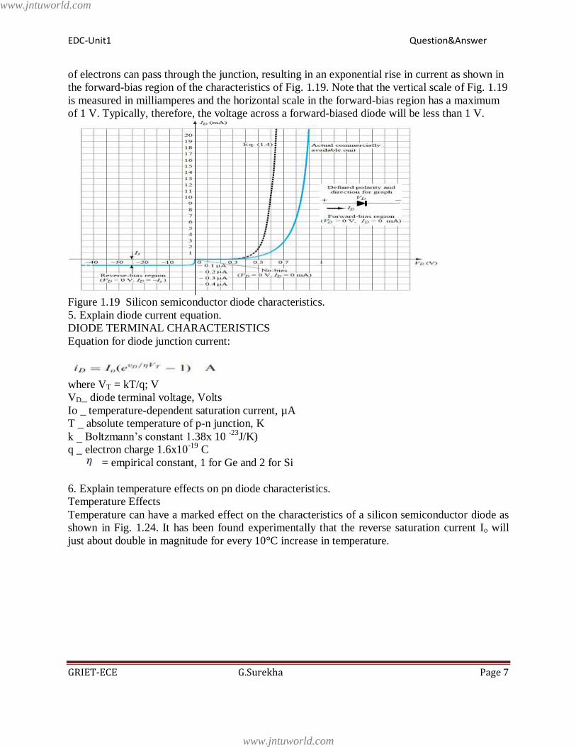
of electrons can pass through the junction, resulting in an exponential rise in current as shown in
the forward-bias region of the characteristics of Fig. 1.19. Note that the vertical scale of Fig. 1.19
is measured in milliamperes and the horizontal scale in the forward-bias region has a maximum
of 1 V. Typically, therefore, the voltage across a forward-biased diode will be less than 1 V.
Figure 1.19 Silicon semiconductor diode characteristics.
5. Explain diode current equation.
DIODE TERMINAL CHARACTERISTICS
Equation for diode junction current:
where VT = kT/q; V
VD_ diode terminal voltage, Volts
Io _ temperature-dependent saturation current, µA
T _ absolute temperature of p-n junction, K
k _ Boltzmann’s constant 1.38x 10 -23
J/K)
q _ electron charge 1.6x10⁻¹⁹
C
= empirical constant, 1 for Ge and 2 for Si
6. Explain temperature effects on pn diode characteristics.
Temperature Effects
Temperature can have a marked effect on the characteristics of a silicon semiconductor diode as
shown in Fig. 1.24. It has been found experimentally that the reverse saturation current Io will
just about double in magnitude for every 10°C increase in temperature.
www.jntuworld.com
www.jntuworld.com

EDC-Unit1 Question&Answer
GRIET-ECE G.Surekha Page 8
Figure 1.24 Variation in diode characteristics with temperature change.
It is not uncommon for a germanium diode with an Io in the order of 1 or 2 A at 25°C to have a
leakage current of 100 A _ 0.1 mA at a temperature of 100°C. Typical values of Io for silicon are
much lower than that of germanium for similar power and current levels. The result is that even
at high temperatures the levels of Io for silicon diodes do not reach the same high levels obtained
for germanium—a very important reason that silicon devices enjoy a significantly higher level of
development and utilization in design. Fundamentally, the open-circuit equivalent in the reverse
bias region is better realized at any temperature with silicon than with germanium. The
increasing levels of Io with temperature account for the lower levels of threshold voltage, as
shown in Fig. 1.24. Simply increase the level of Io in and not rise in diode current. Of course, the
level of TK also will be increase, but the increasing level of Io will overpower the smaller percent
change in TK. As the temperature increases the forward characteristics are actually becoming
more ―ideal,‖ .
7. Explain static resistance and dynamic resistance.
DC or Static Resistance
The application of a dc voltage to a circuit containing a semiconductor diode will result in an
operating point on the characteristic curve that will not change with time. The resistance of the
diode at the operating point can be found simply by finding the Corresponding levels of VD and
ID as shown in Fig. 1.25 and applying the following Equation:
equation (1.5)
The dc resistance levels at the knee and below will be greater than the resistance levels obtained
for the vertical rise section of the characteristics. The resistance levels in the reverse-bias region
will naturally be quite high. Since ohmmeters typically employ a relatively constant-current
source, the resistance determined will be at a preset current level (typically, a few mill amperes).
www.jntuworld.com
www.jntuworld.com

EDC-Unit1 Question&Answer
GRIET-ECE G.Surekha Page 9
Figure 1.25 Determining the dc resistance of a diode at a particular operating point.
AC or Dynamic Resistance
It is obvious from Eq. 1.5 that the dc resistance of a diode is independent of the shape of the
characteristic in the region surrounding the point of interest. If a sinusoidal rather than dc input is
applied, the situation will change completely. The varying input will move the instantaneous
operating point up and down a region of the characteristics and thus defines a specific change in
current and voltage as shown in Fig. 1.27. With no applied varying signal, the point of operation
would be the Q-point appearing on Fig. 1.27 determined by the applied dc levels. The
designation Q-point is derived from the word quiescent, which means ―still or unvarying.‖
Figure 1.27 Defining the dynamic or ac resistance.
A straight line drawn tangent to the curve through the Q-point as shown in Fig. 1.28 will define a
particular change in voltage and current that can be used to determine the ac or dynamic
resistance for this region of the diode characteristics. In equation form,
www.jntuworld.com
www.jntuworld.com
EDC-Unit1 Question&Answer
GRIET-ECE G.Surekha Page 10
Figure 1.28 determining the ac resistance at a Q-point.
8. Draw the diode equivalent circuits and explain.
Diode Equivalent Circuits
An equivalent circuit is a combination of elements properly chosen to best represent the actual
terminal characteristics of a device, system, or such in a particular operating region. In other
words, once the equivalent circuit is defined, the device symbol can be removed from a
schematic and the equivalent circuit inserted in its place without severely affecting the actual
behavior of the system. The result is often a network that can be solved using traditional circuit
analysis techniques.
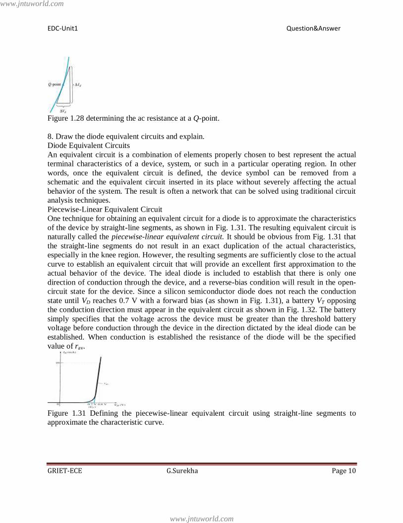
Piecewise-Linear Equivalent Circuit
One technique for obtaining an equivalent circuit for a diode is to approximate the characteristics
of the device by straight-line segments, as shown in Fig. 1.31. The resulting equivalent circuit is
naturally called the piecewise-linear equivalent circuit. It should be obvious from Fig. 1.31 that
the straight-line segments do not result in an exact duplication of the actual characteristics,
especially in the knee region. However, the resulting segments are sufficiently close to the actual
curve to establish an equivalent circuit that will provide an excellent first approximation to the
actual behavior of the device. The ideal diode is included to establish that there is only one
direction of conduction through the device, and a reverse-bias condition will result in the open-
circuit state for the device. Since a silicon semiconductor diode does not reach the conduction
state until VD reaches 0.7 V with a forward bias (as shown in Fig. 1.31), a battery VT opposing
the conduction direction must appear in the equivalent circuit as shown in Fig. 1.32. The battery
simply specifies that the voltage across the device must be greater than the threshold battery
voltage before conduction through the device in the direction dictated by the ideal diode can be
established. When conduction is established the resistance of the diode will be the specified
value of rav.
Figure 1.31 Defining the piecewise-linear equivalent circuit using straight-line segments to
approximate the characteristic curve.
www.jntuworld.com
www.jntuworld.com

EDC-Unit1 Question&Answer
GRIET-ECE G.Surekha Page 11
The approximate level of rav can usually be determined from a specified operating point on the
specification sheet. For instance, for a silicon semiconductor diode, if IF _ 10 mA (a forward
conduction current for the diode) at VD _ 0.8 V, we know for silicon that a shift of 0.7 V is
required before the
characteristics rise.
Simplified Equivalent Circuit
For most applications, the resistance rav is sufficiently small to be ignored in comparison to the
other elements of the network. The removal of rav from the equivalent circuit is the same as
implying that the characteristics of the diode. Under dc conditions has a drop of 0.7 V across it in
the conduction state at any level of diode current.
Ideal Equivalent Circuit
Now that rav has been removed from the equivalent circuit let us take it a step further and
establish that a 0.7-V level can often be ignored in comparison to the applied voltage level. In
this case the equivalent circuit will be reduced to that of an ideal diode as shown in Fig. 1.34
with its characteristics.
www.jntuworld.com
www.jntuworld.com

EDC-Unit1 Question&Answer
GRIET-ECE G.Surekha Page 12
9. Explain Transition capacitance and Diffusion capacitances.
TRANSITION AND DIFFUSION CAPACITANCE
Electronic devices are inherently sensitive to very high frequencies. Most shunt capacitive
effects that can be ignored at lower frequencies because the reactance XC=1/2πfC is very large
(open-circuit equivalent). This, however, cannot be ignored at very high frequencies. XC will
become sufficiently small due to the high value of f to introduce a low-reactance ―shorting‖ path.
In the p-n semiconductor diode, there are two capacitive effects to be considered. In the reverse-
bias region we have the transition- or depletion-region capacitance (CT), while in the forward-
bias region we have the diffusion (CD) or storage capacitance.Recall that the basic equation for
the capacitance of a parallel-plate capacitor is defined by C=€A/d, where € is the permittivity of
the dielectric (insulator) between the plates of area A separated by a distance d. In the reverse-
bias region there is a depletion region (free of carriers) that behaves essentially like an insulator
between the layers of opposite charge. Since the depletion width (d) will increase with increased
reverse-bias potential, the resulting transition capacitance will decrease. The fact that the
capacitance is dependent on the applied reverse-bias potential has application in a number of
electronic systems. Although the effect described above will also be present in the forward-bias
region, it is overshadowed by a capacitance effect directly dependent on the rate at which charge
is injected into the regions just outside the depletion region. The capacitive effects described
above are represented by a capacitor in parallel with the ideal diode, as shown in Fig. 1.38. For
low- or mid-frequency applications (except in the power area), however, the capacitor is
normally not included in the diode symbol.
www.jntuworld.com
www.jntuworld.com
EDC-Unit1 Question&Answer
GRIET-ECE G.Surekha Page 13
10. Explain break down mechanisms in semiconductor diodes.
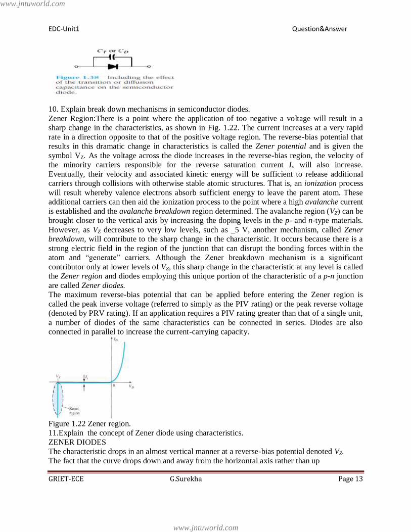
Zener Region:There is a point where the application of too negative a voltage will result in a
sharp change in the characteristics, as shown in Fig. 1.22. The current increases at a very rapid
rate in a direction opposite to that of the positive voltage region. The reverse-bias potential that
results in this dramatic change in characteristics is called the Zener potential and is given the
symbol VZ. As the voltage across the diode increases in the reverse-bias region, the velocity of
the minority carriers responsible for the reverse saturation current Io will also increase.
Eventually, their velocity and associated kinetic energy will be sufficient to release additional
carriers through collisions with otherwise stable atomic structures. That is, an ionization process
will result whereby valence electrons absorb sufficient energy to leave the parent atom. These
additional carriers can then aid the ionization process to the point where a high avalanche current
is established and the avalanche breakdown region determined. The avalanche region (VZ) can be
brought closer to the vertical axis by increasing the doping levels in the p- and n-type materials.
However, as VZ decreases to very low levels, such as _5 V, another mechanism, called Zener
breakdown, will contribute to the sharp change in the characteristic. It occurs because there is a
strong electric field in the region of the junction that can disrupt the bonding forces within the
atom and ―generate‖ carriers. Although the Zener breakdown mechanism is a significant
contributor only at lower levels of VZ, this sharp change in the characteristic at any level is called
the Zener region and diodes employing this unique portion of the characteristic of a p-n junction
are called Zener diodes.
The maximum reverse-bias potential that can be applied before entering the Zener region is
called the peak inverse voltage (referred to simply as the PIV rating) or the peak reverse voltage
(denoted by PRV rating). If an application requires a PIV rating greater than that of a single unit,
a number of diodes of the same characteristics can be connected in series. Diodes are also
connected in parallel to increase the current-carrying capacity.
Figure 1.22 Zener region.
11.Explain the concept of Zener diode using characteristics.
ZENER DIODES
The characteristic drops in an almost vertical manner at a reverse-bias potential denoted VZ.
The fact that the curve drops down and away from the horizontal axis rather than up
www.jntuworld.com
www.jntuworld.com

EDC-Unit1 Question&Answer
GRIET-ECE G.Surekha Page 14
and away for the positive VD region reveals that the current in the Zener region has
a direction opposite to that of a forward-biased diode.
Fig.1.47 zener diode characteristics
Figure 1.48 Conduction direction:
(a) Zener diode; (b) semiconductor diode
This region of unique characteristics is employed in the design of Zener diodes, which have the
graphic symbol appearing in Fig. 1.48a. Both the semiconductor diode and zener diode are
presented side by side in Fig. 1.48 to ensure that the direction of conduction of each is clearly
understood together with the required polarity of the applied voltage. For the semiconductor
diode the ―on‖ state will support a current in the direction of the arrow in the symbol. The
location of the Zener region can be controlled by varying the doping levels. An increase in
doping, producing an increase in the number of added impurities, will decrease the Zener
potential. Zener diodes are available having Zener potentials of 1.8 to 200 V with power ratings
from 14 _ to 50 W. Because of its higher temperature and current capability, silicon is usually
preferred in the manufacture of Zener diodes.
The complete equivalent circuit of the Zener diode in the Zener region includes a small dynamic
resistance and dc battery equal to the Zener potential, as shown in Fig. 1.49.
www.jntuworld.com
www.jntuworld.com

EDC-Unit1 Question&Answer
GRIET-ECE G.Surekha Page 15
Problems
1. A PN Junction diode has a reverse saturation current of 30 A at a temperature of 125 C.
At the same temperature find the dynamic resistance for 0.2V bias in forward and reverse
bias.
Solution: -
Given T = 125 C= 273 + 125=398 K
Io = 30 A VR = - 0/2V, FV = 0.2V. To find out fr = ?
T
f
nVr
I Where
39834.3 .
11600 11600T
TV mv ( )n pp e
and 0 1T
V
VI I e , η = 1 for Ge ; η = 2 for Si.
Case – I When V = - 0.2V.
I = - Io.
fr = VT / I (Taking = 1 for Ge)
fr = 34.3 x 10⁻³
/ 30 x 10-6
= 1143 x 103 = 1143
Case – II When V = 0.2V.
I = 30 x 10-6 3
0.2
34.3 10 1e
= 30 x 10-6
(e 5.831
– 1)
= 30 x 10-6
(341 – 1)
= 30 x 10-6
(340) = 10200 x 10-6
= 10.2 mA.
fr = VT / I =
3
3
34.3 10
10.2 10= 3.36
www.jntuworld.com
www.jntuworld.com
EDC-Unit1 Question&Answer
GRIET-ECE G.Surekha Page 16
2. The voltage across a Germanium diode at room temperature is 0.7 volts and 2 mA
current flows through it. If the voltage across diode increases to 0.75 volts, calculate
diode current. (Assume VT = 26mV)
Solution: -
V = 0.7V, I = 2 mA, T = 300 K, VT = 26 mv.
V = 0.75v, I =?
Case (i) I 0 1T
V
VI I e
= 32 103
0.7
26 100 1I e
= 0I (e26.923
– 1) 0I (e 26.923
)
0I = 3
26.923
2 10
e
Case (ii) 0 1T
V
VI I e
0.753
326 100 26.923
328.846
26.923
3 28.486 26.923
3 1.563
3
2 10
2 10
2 10
2 10
2 10 6.843
13.686 mA
I ee
ee
e
e
www.jntuworld.com
www.jntuworld.com
EDC-Unit1 Question&Answer
GRIET-ECE G.Surekha Page 17
3 For PN diode, the reverse saturation current at a bias of 20V is 20nA. It is 5 A at 75
volts. Calculate DC resistances at these points.
Solution: -
DC resistance DD
D
VR
I
Case (i)
VD = - 20 V, ID = - 20nA.
9
9
2010 1000
20 10
DD
D
VR M
I
Case (ii)
VD = - 75V, ID = - 5 A
6
6
7515 10 15
5 10
DD
D
VR M
I
www.jntuworld.com
www.jntuworld.com