
ECE_468_Report_Sid_AB
13
TWO STAGE AUDIO AMPLIFIER DESIGN ECE 468 FINAL PROJECT REPORT By : Sidharth Kumar (660059012) Abhijeet Solat (672823850)
-
Upload
sidharth-kumar -
Category
Documents
-
view
21 -
download
0
Transcript of ECE_468_Report_Sid_AB

TWO STAGE AUDIO AMPLIFIER DESIGN
ECE 468
FINAL PROJECT REPORT
By :
Sidharth Kumar (660059012)
Abhijeet Solat (672823850)

Objective : To design a Two Channel Audio Amplifier.
The audio amplifier was designed with following specifications of the individual modules :
1. Dual Power Supply : + Vcc (12v) , -Vee (-12V)
2. Volume control : Gain = 1
3. Voltage Amplifier : Common Emitter Configuration, Gain = 10
4. Power Amplifier : Push-Pull Amplifier , Gain = 1
5. LED Panel : 4 LEDs with simple rectifier as the driver.
The second approach to the same design used all the above components except of the fact that
none of the modules used –Vee as a biasing input. The design perspective is described for each
stage in this report. The audio input is considered to be less than 250mV at any point of time and
thus the output voltage of the complete unit can be 2.5V maximum and 0.25V minimum. The gain
ranges from 1 to 10. There is a volume indicator LED panel driven from the output of the power
amplifier module.

1 . DUAL POWER SUPPLY
The most important module for the audio amplifier is the power supply as a constant voltage
source(+12v /-12V here), stepped down from the AC mains high voltage to the value required for
the operation of the various devices like op-amps, diodes, transistors, etc.
The following circuit diagram shows the design of the power supply consisting of :
Step Down transformer.
Bridge Rectifier.
Capacitor assembly for Filtering the ac component from the rectifier output.
Output voltasge : +Vcc = 12V, -Vee = -12V
Simulation Results
Technical approach and designs for individual modules

2. Volume Control using OP-AMP as a summing amplifier
Using an OP-AMP as a summing amplifier gives a freedom of using the resistors for inputs to
be of the value as desired, as on contrary with that of a conventional DAC. The three bit control
of the volume gives the output range from 0.25V to 2.5V in 8 steps (000 to 111 levels of digital
control).
The maximum gain of this circuit is 1, which is due to the fact that the linearity in the output
of a CE amplifier is better than the op-amp. So the required gain is then provided using a
Common Emitter configuration in a cascaded fashion to the output of the volume control unit.
Simulation Output :
UA741

Digits Resistance Gain
000 14.3K 0.07
001 14.3K + 7.5K 0.230
010 14.3K + 3.75K 0.336
100 14.3K + 1.88K 0.602
011 14.3K + (7.5K +3.75K) 0.469
101 14.3K + (1.88K + 7.5K) 0.735
110 14.3 + (1.88K + 3.75K) 0.868
11114.3K + (7.5K + 1.88K +
3.75K)1.00
Gain calculations for 8 levels :

3. Common Emitter configuration for Voltage Amplification
The common emitter configuration of a BJT has an ideal linear region of operation to act as
a voltage amplifier. Thus, we are providing a gain of 10 using the voltage amplifier circuit.
The values mentioned below are not exact in terms of theoretical calculations , as in practical
terms there is a difference in components to be used against the theoretical values.
The resistances R22 and R23 provide the proper biasing to the Base-Emitter junction and
thus fixes the Quiescent point in the linear region to provide undistorted output swing. The
resistances R20 and R21 guide the gain of the amplifier.
Simulation Result :
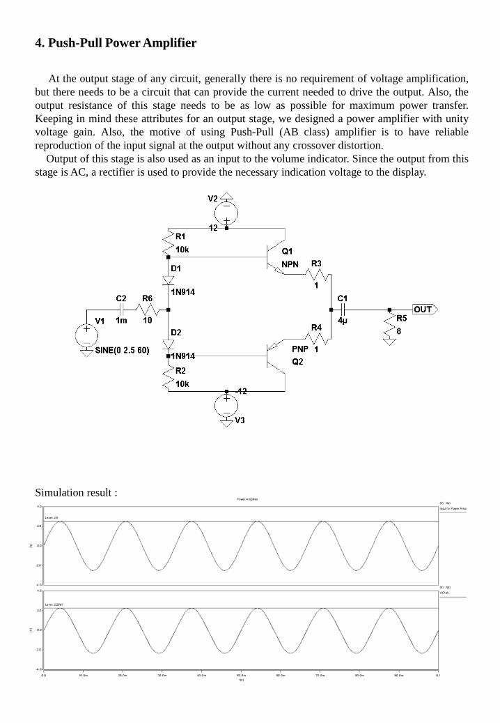
4. Push-Pull Power Amplifier
At the output stage of any circuit, generally there is no requirement of voltage amplification,
but there needs to be a circuit that can provide the current needed to drive the output. Also, the
output resistance of this stage needs to be as low as possible for maximum power transfer.
Keeping in mind these attributes for an output stage, we designed a power amplifier with unity
voltage gain. Also, the motive of using Push-Pull (AB class) amplifier is to have reliable
reproduction of the input signal at the output without any crossover distortion.
Output of this stage is also used as an input to the volume indicator. Since the output from this
stage is AC, a rectifier is used to provide the necessary indication voltage to the display.
Simulation result :
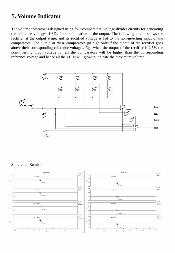
5. Volume Indicator
The volume indicator is designed using four comparators, voltage divider circuits for generating
the reference voltages, LEDs for the indication at the output. The following circuit shows the
rectifier at the output stage, and its rectified voltage is fed to the non-inverting input of the
comparators. The output of these comparators go high only if the output of the rectifier goes
above their corresponding reference voltages. Eg., when the output of the rectifier is 2.5V, the
non-inverting input voltage for all the comparators will be higher than the corresponding
reference voltage and hence all the LEDs will glow to indicate the maximum volume.
Simulation Result :

Complete Circuit and simulation result :

Circuits Diagram for the second approach :
This circuit differs from the previous in the following ways :
1. Transformer used is not centered tapped.
2. The op-amp model used is a Single supply opamp.
3. The LED panel does not employ any kind of logic, but the LEDs used have
breakdown voltages of 0.25, 0.5, 1, 2V.

For On-chip design, the following changes can be made :
1. Power supply to be used can be designed to be a Switch Mode Power supply which is the most
popular power source for CONSTANT DC applications. This shall make the circuit immune to
AC main changes.
2. The Volume control can be realized using a POTENTIOMETER, which operates on the
principle of changing the resistance with a physical knob. In the circuit that we designed, we
can use a variable resistor (pot) at the feedback resistance and thus get a better control over
volume in analog fashion.
3. To realize the voltage amplification on the chip, individual transistor should not be preferred,
instead the IC transistors should be used as the Ics have various protection schemes being
employed to make sure the devices are operating in the region that they are supposed to.
4. Values of the capacitances now being used the design are realistic enough to be available in
electrolytic packages.
5. The power amplifier can be again directly employed as an IC to take the advantage of the
various provisions in the package.
6. The LED panel is simple enough to be directly realized. For the second design considerations,
the LED’s breakdown voltages have to be selected as the requirement for indication.

Hspice Codes
*Voltage_Amp.options post = 1
V1 N005 0 SIN(0 0.25 60)V2 N001 0 12
Q1 N002 N004 N006 normal
R1 N001 N002 4.7kR2 N006 0 280R3 N001 N004 47kR4 N004 0 5.1kR5 OUT 0 10kR6 N003 N005 50
C1 N004 N003 47uC2 OUT N002 2500u
.model normal NPN
.tran 1e-3 100e-3
.end
*Power_Supply.options post = 1
D1 N004 N001 DD2 N001 N005 DD3 N004 N006 DD4 N006 N005 DV1 N002 0 SIN(0 170 60)L1 N003 0 880R1 N003 N002 1L2 N001 0 5L3 0 N006 5C1 N005 0 2mC2 0 N004 2m.model D D Is=150pA n=1.2
K1 L1 L3 1K2 L1 L2 1.tran 1e-3 100e-3.end
* Volume_Control.options post = 1
XU1 0 N003 N004 N005 OUT UA741.include "UA741.301"*Op-amp model - http://www.ti.com/product/ua741V1 N002 0 SIN(0 0.25 60)R1 N002 N003 14.3kR2 N002 N003 1.88kR3 N002 N003 3.75kR4 N002 N003 7.5kR5 OUT N003 1k
V2 N004 0 12V3 N005 0 -12.tran 1e-3 100e-3.end

*Power amplifier.options post=1
Vs 1 0 sin 0 2.5 60
Vdd 4 0 12VVee 5 0 -12V
D1 2 1 diodeD2 1 3 diodeR1 2 4 1kR2 3 5 1kRload 6 0 8.MODEL diode D (Is=18.8n RS=0 BV=400 IBV=5.00u CJO=30p M=0.33 N=2 TT=0)
Q1 4 2 6 BJTN .MODEL BJTN npn+IS=3.88184e-14 BF=929.846 NF=1.10496 VAF=16.5003+IKF=0.019539 ISE=1.0168e-11 NE=1.94752 BR=48.4545+NR=1.07004 VAR=40.538 IKR=0.19539 ISC=1.0168e-11+NC=4 RB=0.1 IRB=0.1 RBM=0.1+RE=0.0001 RC=0.426673 XTB=0.1 XTI=1+EG=1.05 CJE=2.23677e-11 VJE=0.582701 MJE=0.63466+TF=4.06711e-10 XTF=3.92912 VTF=17712.6 ITF=0.4334+CJC=2.23943e-11 VJC=0.576146 MJC=0.632796 XCJC=1+FC=0.170253 CJS=0 VJS=0.75 MJS=0.5+TR=1e-07 PTF=0 KF=0 AF=1
Q2 5 3 6 BJTP.MODEL BJTP pnp+IS=3.02341e-12 BF=523.064 NF=1.16335 VAF=44.2994+IKF=0.591421 ISE=3.31443e-11 NE=1.9954 BR=4.8572+NR=1.18959 VAR=1.33092 IKR=5.91421 ISC=3.31443e-11+NC=3.81262 RB=2.76209 IRB=0.1 RBM=0.880912+RE=0.0001 RC=0.857407 XTB=0.119647 XTI=1+EG=1.05 CJE=3.934e-11 VJE=0.680693 MJE=0.379312+TF=2.75919e-10 XTF=0.674951 VTF=54426.6 ITF=0.067962+CJC=2.40198e-11 VJC=0.4 MJC=0.462796 XCJC=1+FC=0.570446 CJS=0 VJS=0.75 MJS=0.5+TR=1e-07 PTF=0 KF=0 AF=1
.TRAN 10e-6 1
.END


