ECE383: Microcomputers – Lab 1 PCB Artist...
13
1 | P a g e ECE383: Microcomputers – Lab 1 PCB Artist Introduction Goals: The goals of this lab are to introduce students to PCB Artist software to create schematic layouts and generate printed circuit board designs. An additional goal is the creation of a PIC24HJ128GP502 component in PCB Artist. 1. Introduction This lab introduces students to PCB Artist software. PCB is an acronym that stands for Printed Circuit Board. Students will learn how to design electronic circuits using PCB Artist’s schematic tool and then generate a layout of the design using the PCB tool. The final objective will be to design and implement a custom PIC24HJ128GP502 component in PCB Artist. This lab requires you to capture portions of the screen. The lab computers use the Windows 10 operating system. This includes the “Snipping Tool” that may be used to capture portions of the screen. Other third party tools are also available. As always, read through the entire lab and scan the supplied files before starting work. The reporting requirements have you verify your work to the teaching assistant (TA). In all cases, make it easy for the TA to verify your computations by showing your work. Note that this lab can be fully completed outside of the lab and demonstrated to the TA during lab session. 2. PRELAB - TASK 1: Introduction to PCB Artist For this task we will use video tutorials from Advanced Circuits to introduce PCB Artist and its associated schematic capture capabilities. View the seven step-by-step video tutorials located at http://www.4pcb.com/pcb-software- tips-tools.html. These videos reflect the content of the PCB Artist Introduction and Tutorial that can be accessed from the Help->Tutorials->Design Tutorial menu within PCB Artist. Complete chapters 1 and 2 of the tutorial. You will be required to show the TA the completed schematic upon entering the lab. Read the Printed Circuit Board basics tutorial at https://learn.sparkfun.com/tutorials/pcb-basics and answer the following questions. Provide typewritten answers to the following questions. 1. Usually, a PCB is made of four known layers of different materials. Describe the four layers in your own words. 2. Define the following terms in your own words: a) Finger, b) Pad, c) Panel, d) Plated through hole, e) Silkscreen, f) Soldermask, g) Surface mount, and h) Via. TA check: Upon arrival in the lab, show the TA the circuit and the answers you completed. This circuit should closely resemble the completed tutorial circuit given on page 30 of the PCB Artist Introduction and Tutorial document. Include a printout of your circuit and answers in your lab report.
Transcript of ECE383: Microcomputers – Lab 1 PCB Artist...

1 | P a g e
ECE383: Microcomputers – Lab 1 PCB Artist Introduction
Goals: The goals of this lab are to introduce students to PCB Artist software to create schematic layouts and generate printed circuit board designs. An additional goal is the creation of a PIC24HJ128GP502 component in PCB Artist.
1. Introduction
This lab introduces students to PCB Artist software. PCB is an acronym that stands for Printed Circuit Board. Students will learn how to design electronic circuits using PCB Artist’s schematic tool and then generate a layout of the design using the PCB tool. The final objective will be to design and implement a custom PIC24HJ128GP502 component in PCB Artist.
This lab requires you to capture portions of the screen. The lab computers use the Windows 10 operating system. This includes the “Snipping Tool” that may be used to capture portions of the screen. Other third party tools are also available.
As always, read through the entire lab and scan the supplied files before starting work. The reporting requirements have you verify your work to the teaching assistant (TA). In all cases, make it easy for the TA to verify your computations by showing your work. Note that this lab can be fully completed outside of the lab and demonstrated to the TA during lab session.
2. PRELAB - TASK 1: Introduction to PCB Artist
For this task we will use video tutorials from Advanced Circuits to introduce PCB Artist and its associated schematic capture capabilities. View the seven step-by-step video tutorials located at http://www.4pcb.com/pcb-software-tips-tools.html. These videos reflect the content of the PCB Artist Introduction and Tutorial that can be accessed from the Help->Tutorials->Design Tutorial menu within PCB Artist. Complete chapters 1 and 2 of the tutorial. You will be required to show the TA the completed schematic upon entering the lab.
Read the Printed Circuit Board basics tutorial at https://learn.sparkfun.com/tutorials/pcb-basics and answer the following questions. Provide typewritten answers to the following questions.
1. Usually, a PCB is made of four known layers of different materials. Describe the four layers in your own words.
2. Define the following terms in your own words: a) Finger, b) Pad, c) Panel, d) Plated through hole, e) Silkscreen, f) Soldermask, g) Surface mount, and h) Via.
TA check: Upon arrival in the lab, show the TA the circuit and the answers you completed. This circuit should closely resemble the completed tutorial circuit given on page 30 of the PCB Artist Introduction and Tutorial document. Include a printout of your circuit and answers in your lab report.
2 | P a g e
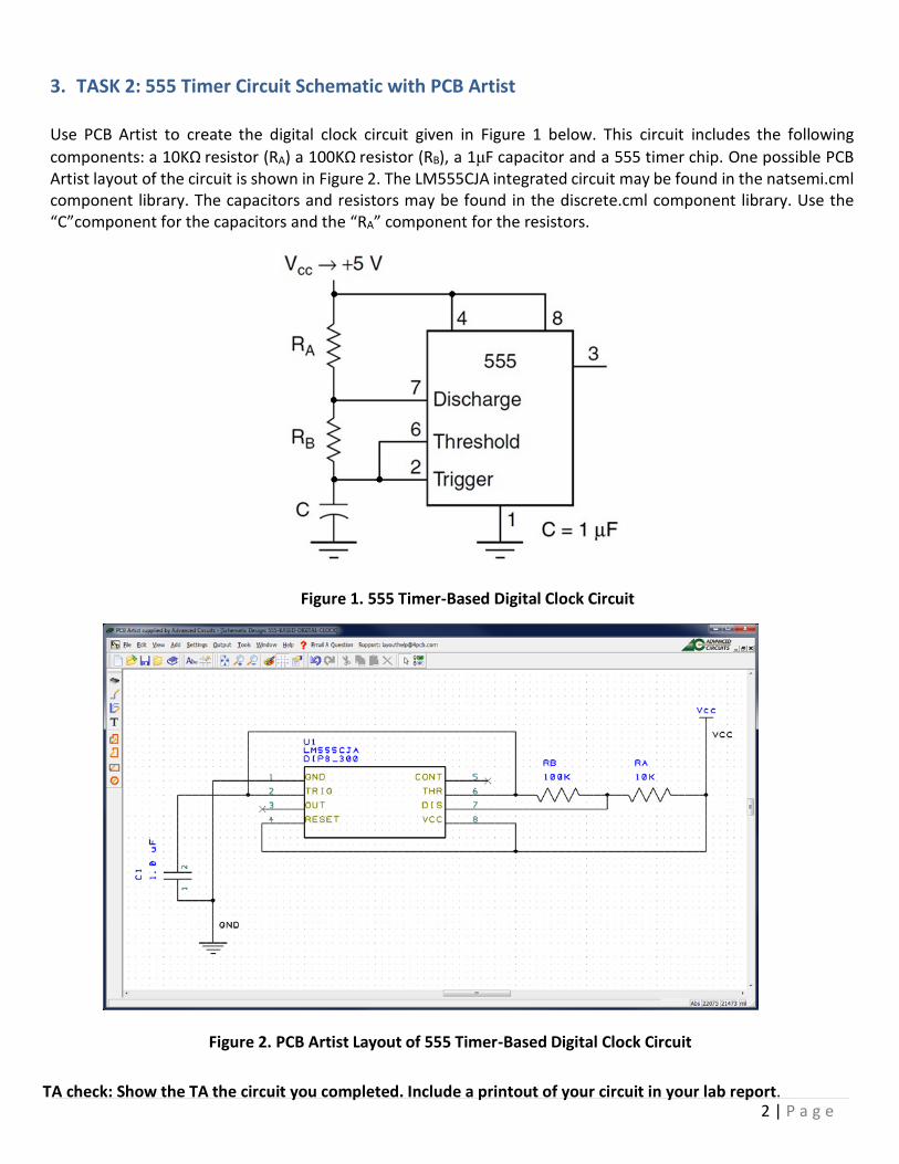
3. TASK 2: 555 Timer Circuit Schematic with PCB Artist
Use PCB Artist to create the digital clock circuit given in Figure 1 below. This circuit includes the following components: a 10KΩ resistor (RA) a 100KΩ resistor (RB), a 1μF capacitor and a 555 timer chip. One possible PCB Artist layout of the circuit is shown in Figure 2. The LM555CJA integrated circuit may be found in the natsemi.cml component library. The capacitors and resistors may be found in the discrete.cml component library. Use the “C”component for the capacitors and the “RA” component for the resistors.
Figure 1. 555 Timer-Based Digital Clock Circuit
Figure 2. PCB Artist Layout of 555 Timer-Based Digital Clock Circuit
TA check: Show the TA the circuit you completed. Include a printout of your circuit in your lab report.

3 | P a g e
4. TASK 3: Creation of a Printed Circuit Board Layout with PCB Artist For this task we will create a printed circuit board layout from the digital clock circuit schematic created as a part of task 2. Chapter 4 of the PCB Artist Introduction and Tutorial describes the basic process of converting the circuit schematic into a printed circuit board layout. Read from the beginning of chapter 4 to the section titled “Unrouting the design”. Use the described process using the Schematic To PCB wizard within PCB Artist. You can accept all the default choices provided by the wizard until the “Place and Route” dialog box is shown. Select “Arrange Outside the Board” for component placement and select “Next”. This will result in a PCB that will be similar to the diagram shown in Figure 3 below.
Figure 3. PCB Wizard Generated Design with Components Unplaced and Nets Unrouted Select Tools->Auto Place Components->All Components to have PCB Artist auto-place all the circuit components onto the PCB. Select Tools->Auto Route Nets->All Nets to have PCB Artist auto-route all the circuit networks (i.e. connections between components) on the PCB. This will result in a printed circuit board similar to the one shown in Figure 4 below.

4 | P a g e
Figure 4. Printed Circuit Board with all Components Placed and all Nets Routed
TA check: Show the TA the printed circuit board you completed. Include a printout of your PCB in your lab report.
5. TASK 4: PIC24HJ128GP502 Schematic Symbol, PCB Footprint, and Component in PCB Artist
For this task you will create a component for the PIC24HJ128GP502 microcontroller in PCB Artist. Begin by reading and completing the Library Creation Tutorial within PCB Artist (Help->Tutorials->Part Creation Tutorial). After completing the tutorial, perform the following steps:
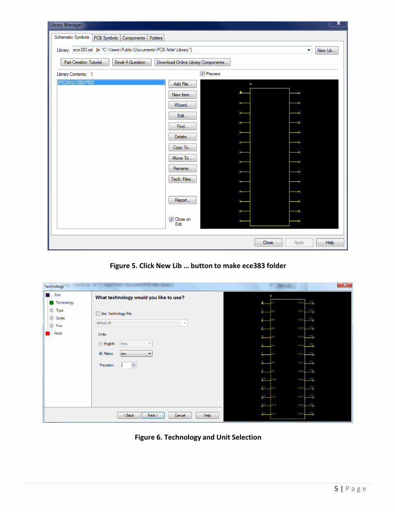
• Within the Library Manager, create a new schematic symbol library called ece383.ssl. Use the Symbol Wizard tool to create a schematic symbol called PIC24HJ128GP502. Example screen captures for this wizard are shown below.
5 | P a g e
Figure 5. Click New Lib … button to make ece383 folder
Figure 6. Technology and Unit Selection

6 | P a g e
Figure 7. Symbol Type, Origin, and Component Name Position
Figure 8. Symbol Pin and Line Styles

7 | P a g e
Figure 9. Pin Layout
Figure 10. Symbol Naming and Final Creation Step
• Within the Library Manager, create a new component library called ece383.cml. Use the Component Wizard tool to create a component called PIC24HJ128GP502. Example screen captures for this wizard are shown below.

8 | P a g e
Figure 11. Click New Lib… to make ece383.cml file in components tab
Figure 12. Create a Normal Component Type
9 | P a g e
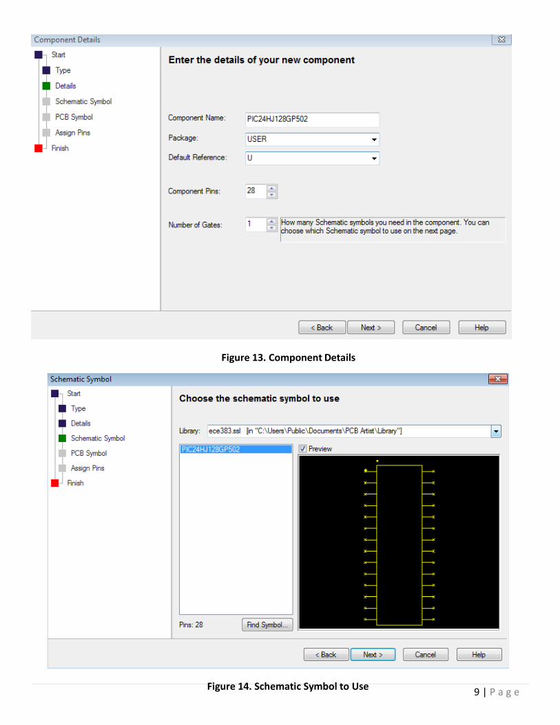
Figure 13. Component Details
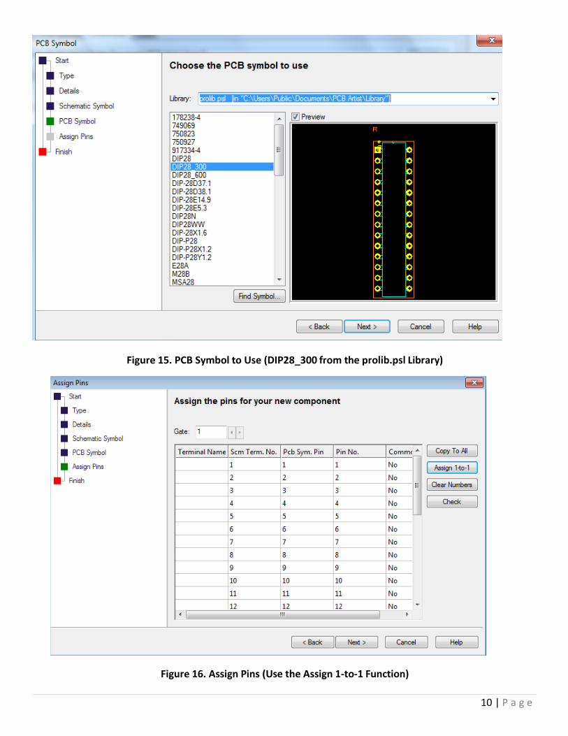
Figure 14. Schematic Symbol to Use
10 | P a g e
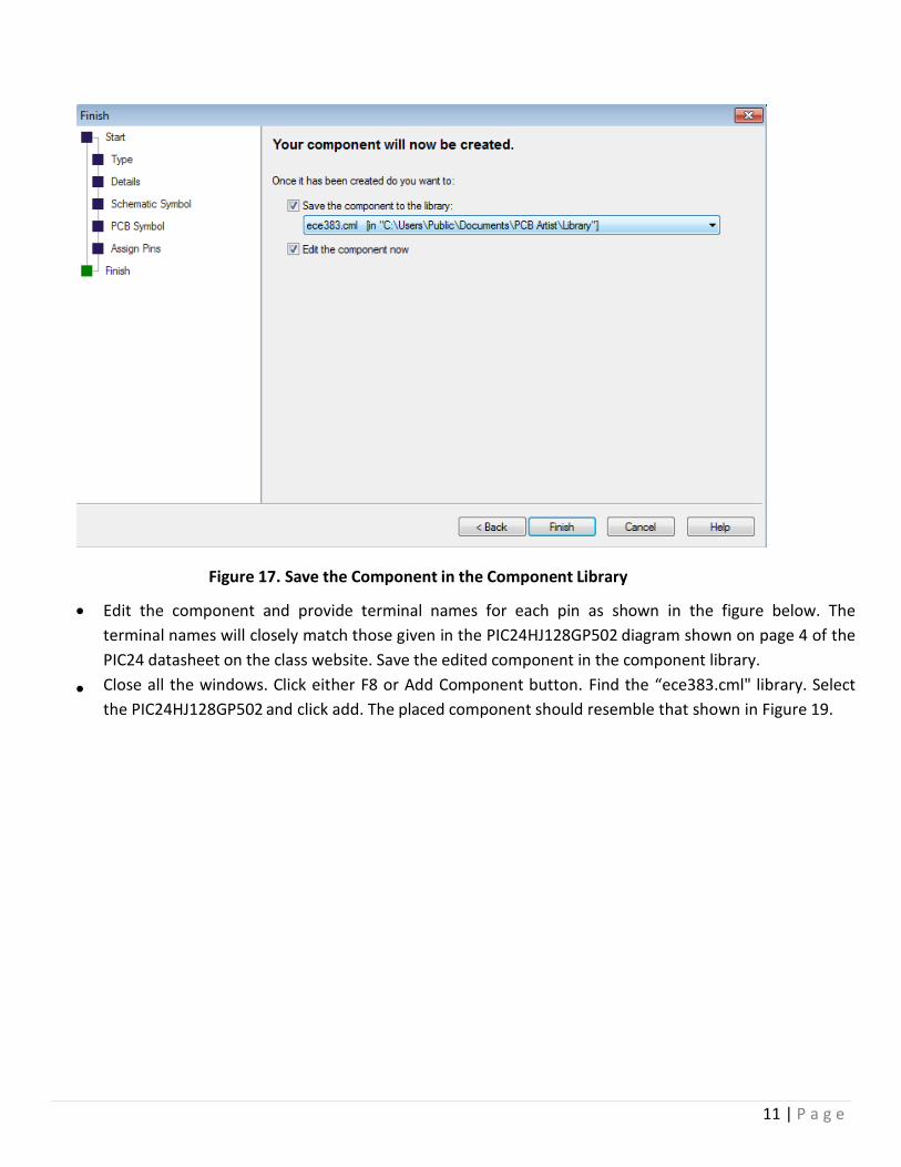
Figure 15. PCB Symbol to Use (DIP28_300 from the prolib.psl Library)
Figure 16. Assign Pins (Use the Assign 1-to-1 Function)
11 | P a g e
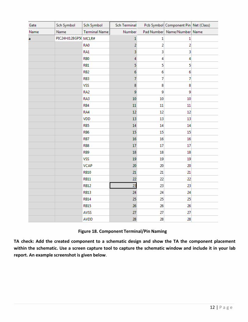
Figure 17. Save the Component in the Component Library
• Edit the component and provide terminal names for each pin as shown in the figure below. The terminal names will closely match those given in the PIC24HJ128GP502 diagram shown on page 4 of the PIC24 datasheet on the class website. Save the edited component in the component library.
• Close all the windows. Click either F8 or Add Component button. Find the “ece383.cml" library. Select the PIC24HJ128GP502 and click add. The placed component should resemble that shown in Figure 19.
12 | P a g e
Figure 18. Component Terminal/Pin Naming TA check: Add the created component to a schematic design and show the TA the component placement within the schematic. Use a screen capture tool to capture the schematic window and include it in your lab report. An example screenshot is given below.

15 | P a g e
Figure 19. PIC24HJ128GP502 Placement in a Schematic 6. Laboratory Report
No later than a week from the day the lab is performed, provide the TA a printed copy of a lab report following the ECE383 Lab report Template given on the class website. Each lab group will submit one joint lab report to the TA. Your report should have the reporting requirements needed for Tasks 1, 2, 3 and 4.
7. GRADING POLICY
1. Completion of the pre-lab assignment (Task 1) with results included in lab report (20%) 2. Completion of Task 2 with results included in lab report (20%) 3. Completion of Task 3 with results included in lab report (20%) 4. Completion of Task 4 with results included in lab report (20%) 5. Completeness, quality, and correctness of the lab report (20%)


![Music, Mathematics, and Microcomputers · Music, Mathematics, and Microcomputers ... and elaborated by Knud Jeppesen [12]. ... melodic, and counterpoint rules, is it](https://static.fdocuments.in/doc/165x107/5b4913d27f8b9ab1228b5150/music-mathematics-and-microcomputers-music-mathematics-and-microcomputers.jpg)