
ECE331 Wi06 Kronig-Penney Modellu/ECE331_Wi06_lec_10.pdf · ECE331_Wi06 Kronig-Penney Model The 1-D...
8
1 Lu ECE331_Wi06 Kronig-Penney Model The 1-D potential function can be simplified as a series of potential barriers with an identical barrier width and period. Lu ECE331_Wi06 E-K Diagram in Kronig-Penney Model To have solutions, we have energy bands and gaps.
Transcript of ECE331 Wi06 Kronig-Penney Modellu/ECE331_Wi06_lec_10.pdf · ECE331_Wi06 Kronig-Penney Model The 1-D...
1
Lu
ECE331_Wi06
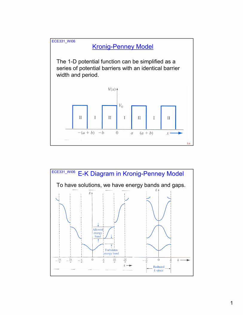
Kronig-Penney Model
The 1-D potential function can be simplified as a series of potential barriers with an identical barrier width and period.
Lu
ECE331_Wi06 E-K Diagram in Kronig-Penney Model
To have solutions, we have energy bands and gaps.
2
Lu
ECE331_Wi06
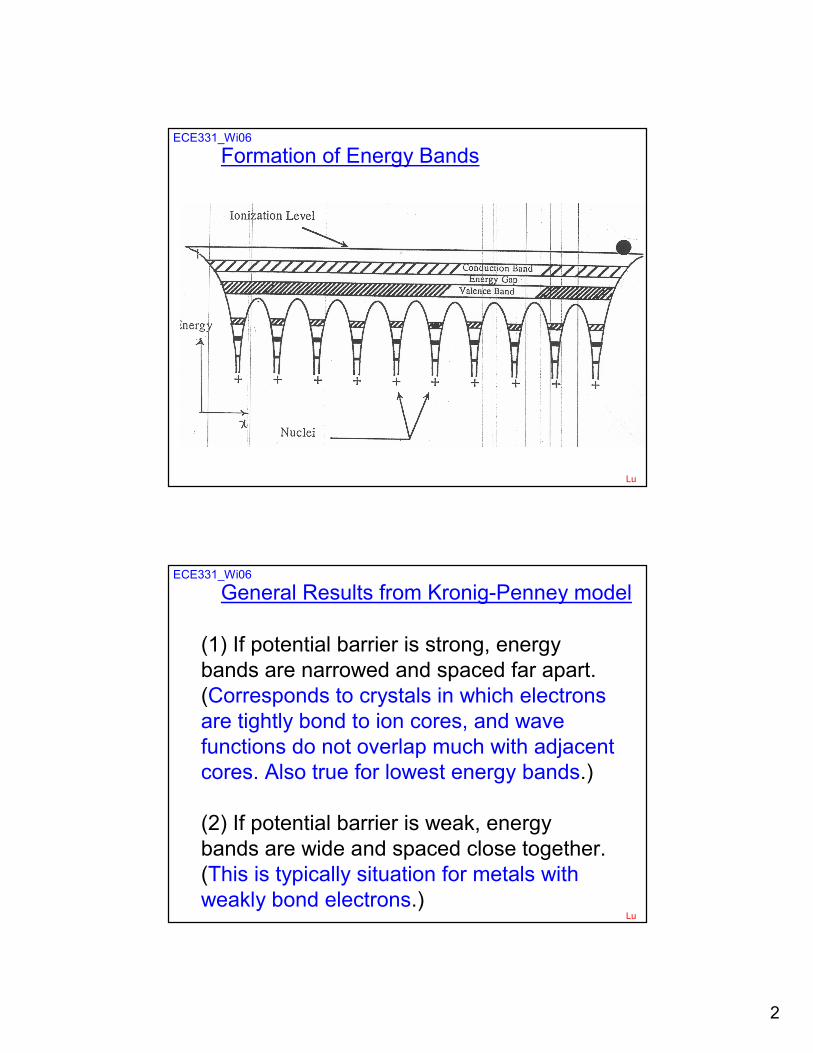
Formation of Energy Bands
In Reg. I,
Lu
ECE331_Wi06
General Results from Kronig-Penney model
(1) If potential barrier is strong, energy bands are narrowed and spaced far apart. (Corresponds to crystals in which electrons are tightly bond to ion cores, and wave functions do not overlap much with adjacent cores. Also true for lowest energy bands.)
(2) If potential barrier is weak, energy bands are wide and spaced close together. (This is typically situation for metals with weakly bond electrons.)
3
Lu
ECE331_Wi06
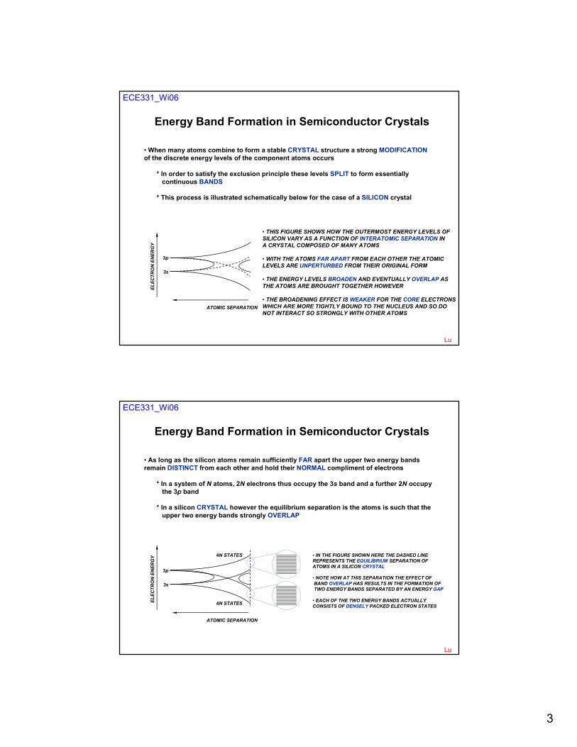
Energy Band Formation in Semiconductor Crystals
• When many atoms combine to form a stable CRYSTAL structure a strong MODIFICATIONof the discrete energy levels of the component atoms occurs
* In order to satisfy the exclusion principle these levels SPLIT to form essentiallycontinuous BANDS
* This process is illustrated schematically below for the case of a SILICON crystal
3s
3p
ELEC
TRO
N E
NER
GY
ATOMIC SEPARATION
• THIS FIGURE SHOWS HOW THE OUTERMOST ENERGY LEVELS OFSILICON VARY AS A FUNCTION OF INTERATOMIC SEPARATION INA CRYSTAL COMPOSED OF MANY ATOMS
• WITH THE ATOMS FAR APART FROM EACH OTHER THE ATOMICLEVELS ARE UNPERTURBED FROM THEIR ORIGINAL FORM
• THE ENERGY LEVELS BROADEN AND EVENTUALLY OVERLAP ASTHE ATOMS ARE BROUGHT TOGETHER HOWEVER
• THE BROADENING EFFECT IS WEAKER FOR THE CORE ELECTRONSWHICH ARE MORE TIGHTLY BOUND TO THE NUCLEUS AND SO DONOT INTERACT SO STRONGLY WITH OTHER ATOMS
Lu
ECE331_Wi06
• As long as the silicon atoms remain sufficiently FAR apart the upper two energy bands remain DISTINCT from each other and hold their NORMAL compliment of electrons
* In a system of N atoms, 2N electrons thus occupy the 3s band and a further 2N occupythe 3p band
* In a silicon CRYSTAL however the equilibrium separation is the atoms is such that theupper two energy bands strongly OVERLAP
• IN THE FIGURE SHOWN HERE THE DASHED LINEREPRESENTS THE EQUILIBRIUM SEPARATION OFATOMS IN A SILICON CRYSTAL
• NOTE HOW AT THIS SEPARATION THE EFFECT OF BAND OVERLAP HAS RESULTS IN THE FORMATION OF TWO ENERGY BANDS SEPARATED BY AN ENERGY GAP
• EACH OF THE TWO ENERGY BANDS ACTUALLYCONSISTS OF DENSELY PACKED ELECTRON STATES
Energy Band Formation in Semiconductor Crystals
3s
3p
ELEC
TRO
N E
NER
GY
ATOMIC SEPARATION
4N STATES
4N STATES
4
Lu
ECE331_Wi06
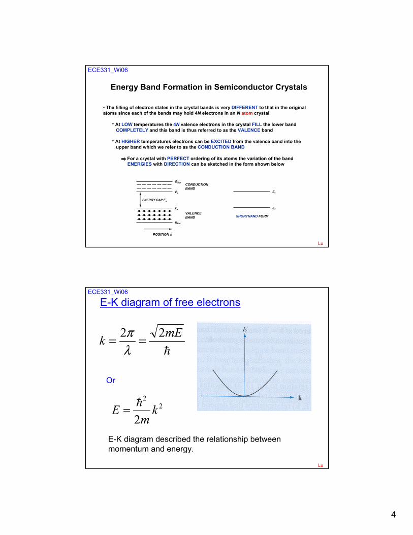
• The filling of electron states in the crystal bands is very DIFFERENT to that in the original atoms since each of the bands may hold 4N electrons in an N atom crystal
* At LOW temperatures the 4N valence electrons in the crystal FILL the lower bandCOMPLETELY and this band is thus referred to as the VALENCE band
* At HIGHER temperatures electrons can be EXCITED from the valence band into theupper band which we refer to as the CONDUCTION BAND
⇒⇒⇒⇒ For a crystal with PERFECT ordering of its atoms the variation of the bandENERGIES with DIRECTION can be sketched in the form shown below
Energy Band Formation in Semiconductor Crystals
ENERGY GAP Eg
POSITION x
EBot
Ev
Ec
ETopCONDUCTIONBAND
VALENCEBAND
Ev
Ec
SHORTHAND FORM
Lu
ECE331_Wi06
E-K diagram of free electrons
�
mEk 22 ==λπ
E-K diagram described the relationship between momentum and energy.
Or
22
2k
mE �=
5
Lu
ECE331_Wi06
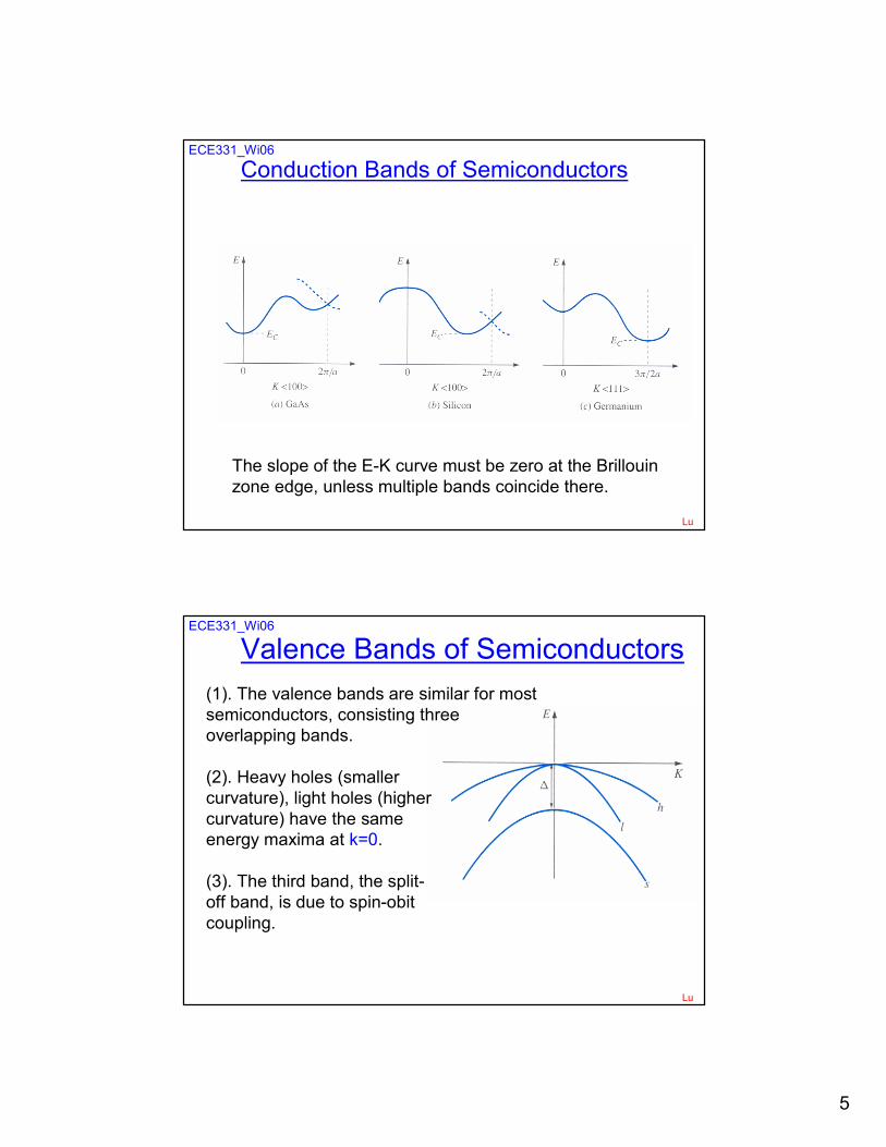
Conduction Bands of Semiconductors
In Reg. I,
In Reg. II, V0 = 2E
The slope of the E-K curve must be zero at the Brillouinzone edge, unless multiple bands coincide there.
Lu
ECE331_Wi06
Valence Bands of Semiconductors(1). The valence bands are similar for most semiconductors, consisting threeoverlapping bands.
(2). Heavy holes (smallercurvature), light holes (highercurvature) have the sameenergy maxima at k=0.
(3). The third band, the split-off band, is due to spin-obitcoupling.
6
Lu
ECE331_Wi06
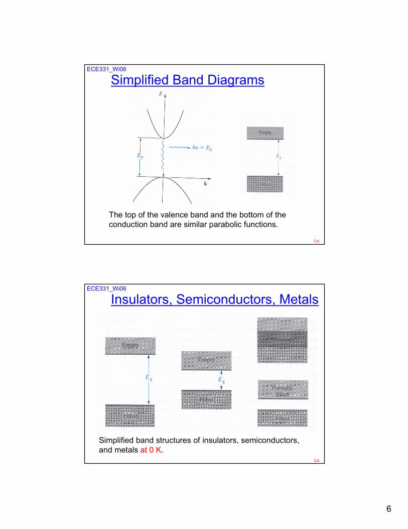
Simplified Band Diagrams
The top of the valence band and the bottom of the conduction band are similar parabolic functions.
Lu
ECE331_Wi06
Insulators, Semiconductors, Metals
Simplified band structures of insulators, semiconductors, and metals at 0 K.
7
Lu
ECE331_Wi06
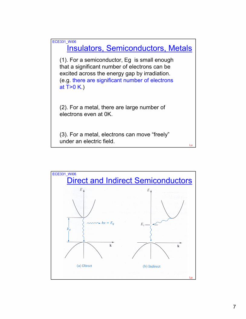
Insulators, Semiconductors, Metals(1). For a semiconductor, Eg is small enough that a significant number of electrons can be excited across the energy gap by irradiation. (e.g. there are significant number of electrons at T>0 K.)
(2). For a metal, there are large number of electrons even at 0K.
(3). For a metal, electrons can move “freely” under an electric field.
Lu
ECE331_Wi06
Direct and Indirect Semiconductors
8
Lu
ECE331_Wi06
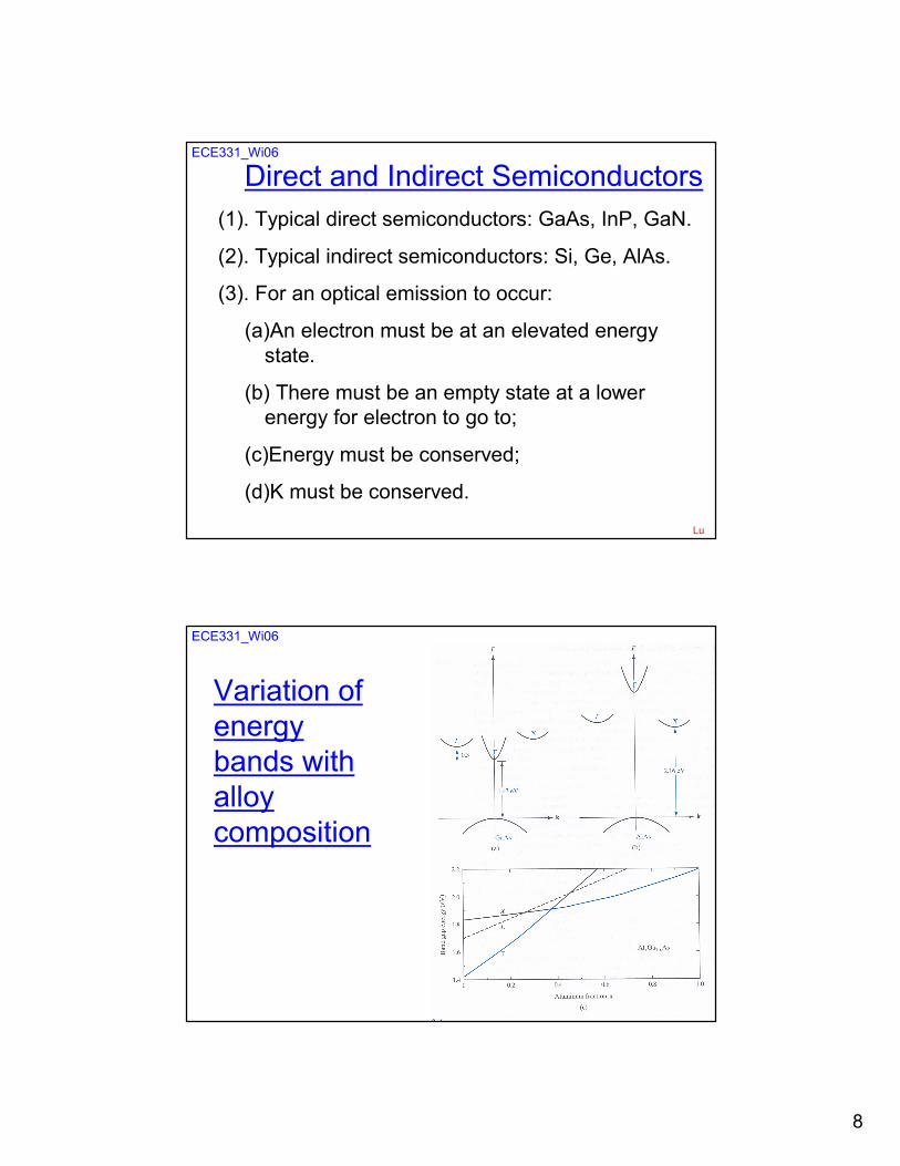
Direct and Indirect Semiconductors(1). Typical direct semiconductors: GaAs, InP, GaN.
(2). Typical indirect semiconductors: Si, Ge, AlAs.
(3). For an optical emission to occur:
(a)An electron must be at an elevated energy state.
(b) There must be an empty state at a lower energy for electron to go to;
(c)Energy must be conserved;
(d)K must be conserved.
Lu
ECE331_Wi06
Variation of energy bands with alloy composition