ECE251: Tuesday October 15 · • Resolution: 48 x 84 pixels (height x width) 6 rows of 14...
24
Lecture #15 1 ECE251: Tuesday October 15 • Serial I/O – Serial I/O Introduction/Overview – SSI Interface Details – Chapter 22 in text, but only for general concepts – TM4C Data Sheet, Chapters 14 and 15 • HW #4 Due October 24—Question added on October 10 after mid-term exam • Lab Practical This Week. • Lab #4 Due Next Week—Week of October 21 • Lab #5 (Serial I/O) Begins Next Week
Transcript of ECE251: Tuesday October 15 · • Resolution: 48 x 84 pixels (height x width) 6 rows of 14...

Lecture #15 1
ECE251: Tuesday October 15• Serial I/O
– Serial I/O Introduction/Overview– SSI Interface Details– Chapter 22 in text, but only for general concepts– TM4C Data Sheet, Chapters 14 and 15
• HW #4 Due October 24—Question added on October 10 after mid-term exam
• Lab Practical This Week.• Lab #4 Due Next Week—Week of October 21• Lab #5 (Serial I/O) Begins Next Week

Lecture #15 2
Serial Communications• Two Fundamental Types
– Synchronous: TM4C SSI– Asynchronous: TM4C UART
• In all serial communications– A single communication line is used for the
communication– Data is sent and received as a string of single bits– For reliable communication, strict communication
protocols and timing schemes are followed.

Lecture #15 3
Parallel (vs. Serial) Communications
• Multiple bits are sent and received simultaneously, e.g. GPIO.• A separate line is provided for each data bit + control signals• Generally its faster than serial communication.• Increases the amount of hardware.• Requires more transmission paths• Becoming less used (vs. USB, ethernet, etc.)
R/W*
Timing
8-bit data
Device 1 Device 2

Lecture #15 4
Serial Communications• One signal line (possibly one each way)• Both signal and clock in synchronous communication• Great for long distance communication• Very Good even for very short communication• Lower speed than parallel, but may be very fast (5 Gbit/sec USB 3.0)• Low cost vs. many wires
1 bit
Device 1 Device 2
Clk Shift Register Shift Register
8 bits 8 bits
Clk

Lecture #15 5
Synchronous Serial Interface (SSI)Serial Peripheral Interface (SPI) is example in text
• Synchronous serial communication system means:• Transmitter and receiver share a common clock• MASTER = Clock signal provider. Feeds clock to
Slave devices. Info can go either/both directions.• SSI operates as a geographically distributed shift
register – see later slide.• LOTS of external devices use this protocol.
Important: Basis for Lab #5.• For detailed information see:
Text, Section 22.3 and TM4C Data Sheet, Section 15.

Lecture #15 6
TM4C SSI Module Block Diagram

Lecture #15 7
TM4C SSI External Connections

Lecture #15 8
Serial Interface Signal Names
• SSI acts as 16-bit distributed shift register, sharing a clock provided by the Master
• Uses System or Precision Clock (We’ll discuss later)• TM4C SSI Signals (and SPI Names)
– SSInCLK or SCLK: Serial shift clock– SSInTx or MOSI: Master Out-Slave in (from master to slave)– SSInRx or MISO: Master In-Slave out (from slave to master)– SSInFss or FSS: Tells slave that data is being sent (serial
frame pin)
16-bit shift register configured for rotate right operationand split into two separate 8-bit shift registers
MOSI
MISO

Lecture #15 9
Serial Interface Signals-Timing
• Master needs to know when slave will send a response and how long the response will be

Lecture #15 10
Multiple Slaves
Master is able to send data to multiple slaves by controlling each Slave Select line

Lecture #15 11
TM4C SSI Capabilities• Four SSI Modules for four concurrent synchronous serial
communication activities.• Performs serial-to-parallel conversion on input and
parallel-to-serial conversion on output. How?• Internal FIFO memories: up to eight 16-bit values. • Bit Rate Generation with programmable clock divider and
prescaling.• Multiple Programmable protocols: Freescale SPI,
MICROWIRE or TI Synchronous.• Programmable data frame size: 4-16 bits.• FIFO-based and End-of-Transmission interrupts available.
– We won’t be using interrupts in this lab.
Lecture #15 12
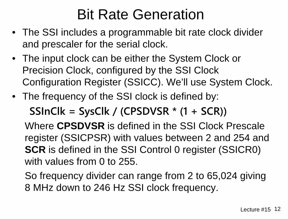
Bit Rate Generation• The SSI includes a programmable bit rate clock divider
and prescaler for the serial clock.• The input clock can be either the System Clock or
Precision Clock, configured by the SSI Clock Configuration Register (SSICC). We’ll use System Clock.
• The frequency of the SSI clock is defined by:SSInClk = SysClk / (CPSDVSR * (1 + SCR))
Where CPSDVSR is defined in the SSI Clock Prescaleregister (SSICPSR) with values between 2 and 254 and SCR is defined in the SSI Control 0 register (SSICR0) with values from 0 to 255.So frequency divider can range from 2 to 65,024 giving 8 MHz down to 246 Hz SSI clock frequency.

Lecture #15 13
“Freescale SPI” SSI Signal Format (used in Lab #5)
Sequence begins on falling edge and ends on rising edgeRising clock: latch of Rx, Tx signals
Falling clock: new Rx and Tx signals

Lecture #15 14
SSI Pins and Setup• GPIO Pins are used, so GPIO must be set up
– Enable Port A using RCGCGPIO register to start GPIO clock– Alternate Function Register (AFSEL) set for use of pins by SSI– Set pin direction as appropriate with DIR, enable digital signals with DEN, and
disable analog functionality with AMSEL, just like when GPIO is used– Configure port pins as SSI with GPIOPCTL register
• Set up SSI functionality– Enable with RCGCSSI to start appropriate SSI clock– Temporarily disable SSI functionality using SSICR1 (clear SSE bit) and set to
Master/Slave as appropriate with MS bit (clear for Master)– Set Data Bit Rate using SSICPSR, SSICC, and SSICR0 registers (already
discussed)– Determine size of data register using DSS bits of SSICR0– Specify Frame Format using SSICR0 register– Enable SSI using SSICR1 register.
• A detailed setup explanation is in Lab 5: Sections 5.3-5.4

Lecture #15 15
Alternate Function Table (Partial)

Lecture #15 16
Reading the Alternate Function Table

NOKIA 5110 LCD• Low power CMOS LCD module• Phillips PCD8544 controller• Resolution: 48 x 84 pixels
(height x width) 6 rows of 14 characters• Dot Matrix display, 1-bit per pixel• 48 × 84 bit static RAM internal to the
PCD8554 which stores the display data.• Device driver library Nokia5110.s (provided to
you) uses the Freescale SPI protocol• Max Transfer Rate 4 Mbps (way, way fast!)
– Almost 1000 full frames/second
Lecture #16 17

Lecture #15 18
GPIO/SSI Setup Example• The following slides show code structure used to set up SSI
and GPIO for the 5110 Graphic Display, as used in lab #5.• This Graphic Display will be explained in much more detail in
the following lecture. • For more information on this Graphic Display, see the Nokia
5110 Data Sheet on our Lab website.• GPIO Port A pins 2,3,5,6,7 and SSI Channel 0 are used
– PA 2,3 and 5 used as SSI pins• PA2, pin 19: SSI0Clk Clock to 5110• PA3, pin 20: SSI0Fss Slave Select for 5110• PA5, pin 22: SSI0Tx MOSI to 5110• MISO signal not used with 5110. Why not? No return data is needed.
– Pins 6 and 7 used as GPIO pins• PA6, pin 23: Data/Command signal to 5110• PA7, pin 24: Reset signal to 5110

Lecture #15 19
GPIO/SSI Setup: Pins & GPIO Registers; Pin connections; ------------------------------------------; Signal (Nokia 5110) TIVA LaunchPad pin; ------------------------------------------; 3.3V (VCC, pin 1) power; Ground (GND, pin 2) ground; SSI0Fss (SCE, pin 3) connected to PA3 (SSI) Serial Frame Pin (Selects Nokia system); Reset (RST, pin 4) connected to PA7 (GPIO); Data/Command (D/C, pin 5) connected to PA6 (GPIO); SSI0Tx (DN, pin 6) connected to PA5 (SSI) MOSI Serial Data ; SSI0Clk (SCLK,pin 7) connected to PA2 (SSI) Clock signal to Nokia; back light (LED, pin 8) not connected, consists of 4 white LEDs which draw ~80mA total
;GPIO RegistersGPIO_PORTA_DATA EQU 0x400043FC ; Port A DataGPIO_PORTA_IM EQU 0x40004410 ; Interrupt MaskGPIO_PORTA_DIR EQU 0x40004400 ; Port DirectionGPIO_PORTA_AFSEL EQU 0x40004420 ; Alt Function enableGPIO_PORTA_DEN EQU 0x4000451C ; Digital EnableGPIO_PORTA_AMSEL EQU 0x40004528 ; Analog enableGPIO_PORTA_PCTL EQU 0x4000452C ; Alternate Functions

Lecture #15 20
GPIO/SSI Setup: SSI Registers;SSI RegistersSSI0_CR0 EQU 0x40008000 ; SSI Control Register 0SSI0_CR1 EQU 0x40008004 ; SSI Control Register 1SSI0_DR EQU 0x40008008 ; SSI Data RegisterSSI0_SR EQU 0x4000800C ; SSI Status RegisterSSI0_CPSR EQU 0x40008010 ; SSI Clock PrescalerSSI0_CC EQU 0x40008FC8 ; SSI Clock Configuration
;System RegistersSYSCTL_RCGCGPIO EQU 0x400FE608 ; GPIO Gate ControlSYSCTL_RCGCSSI EQU 0x400FE61C ; SSI Gate Control
• Following Slides give outline and some detail of configuring GPIO and SSI for the Nokia system. You are asked to supply the missing configuration details in this code.

Lecture #15 21
GPIO SetupNokia_Init ; Subroutine to initialize Nokia
PUSH {LR};Setup GPIO
LDR R1, =SYSCTL_RCGCGPIO ; GPIO clock startupLDR R0, [R1] ORR R0, R0, #0x01 ; set bit 0 for port ASTR R0, [R1] NOP ; allow clock to settleNOPNOPLDR R1,=GPIO_PORTA_DIR ; make PA 2,3,5,6,7 outputMOV R0,#0xEC ; and PA 4 inputSTR R0,[R1]LDR R1,=GPIO_PORTA_AFSEL ; enable alternate functionality
; on PA 2,3,4,5 Missing Code for; Leave 6,7 as GPIO pins You to Fill In
LDR R1,=GPIO_PORTA_DEN ; enable digital I/O; on pins 7-2 “;
LDR R1,=GPIO_PORTA_PCTL ; configure PA 2,3,4,5 as SSILDR R0,=0x00222200 ; pins 5-2 (bits 23-8)STR R0,[R1]LDR R1,=GPIO_PORTA_AMSEL ; disable analog functionality Etc
;;

Lecture #15 22
SSI Setup;Setup SSI
LDR R1,=SYSCTL_RCGCSSI ; Code to start SSI clock;; set bit 0 for SSI0 Missing Code ;
MOV R0,#0x0FwaitSSIClk ; allow clock to settle
SUBS R0,R0,#0x01BNE waitSSIClkLDR R1,=SSI0_CR1 ; disable SSI during setup
; also set to Master Missing Code ;
; Configure baud rate PIOSC=16MHz,Baud=2MHz,CPSDVSR=4,SCR=1; BR=SysClk/(CPSDVSR * (1 + SCR)) = 16MHz/(4*(1+1)) = ? MHz
LDR R1,=SSI0_CC ; use PIOSC (16MHz); Missing Code
LDR R1,=SSI0_CR0 ; set SCR to 0x01LDR R0,[R1] ; update appropriate bits of CR0
; Missing Code LDR R1,=SSI0_CPSR ; set CPSDVSR (prescale) “

Lecture #15 23
SSI Setup continued;Setup SSI continued
LDR R1,=SSI0_CR0 ; choose Freescale frame format LDR R0,[R1] ; clearing SPH and SPO*BIC R0,#0xF0ORR R0,R0,#0x07 ; 8-bit dataSTR R0,[R1]LDR R1,=SSI0_CR1 ; enable SSILDR R0,[R1] ; updating correct bit ;
; SSI Setup Complete
Definitions of SPO relates to Clock Polarity and SPH relates to Clock Phase Control with the Freescale frame format. This will be the format required by the Nokia 5110 protocol. See Section 15.3.4.2 of TM4C Data Sheet for more information.
• Note: still need setup code for Nokia—next lecture

Lecture #15 24
Next Lecture• NOKIA 5110 Graphics Subsystem
– Graphics Organization– Setup & Sending Commands to Nokia Controller– Sending Data
• Text• Graphics