ECE102B BASICS OF ELECTRONICS …... using Basic gates and universal gates ... • Design and...
57
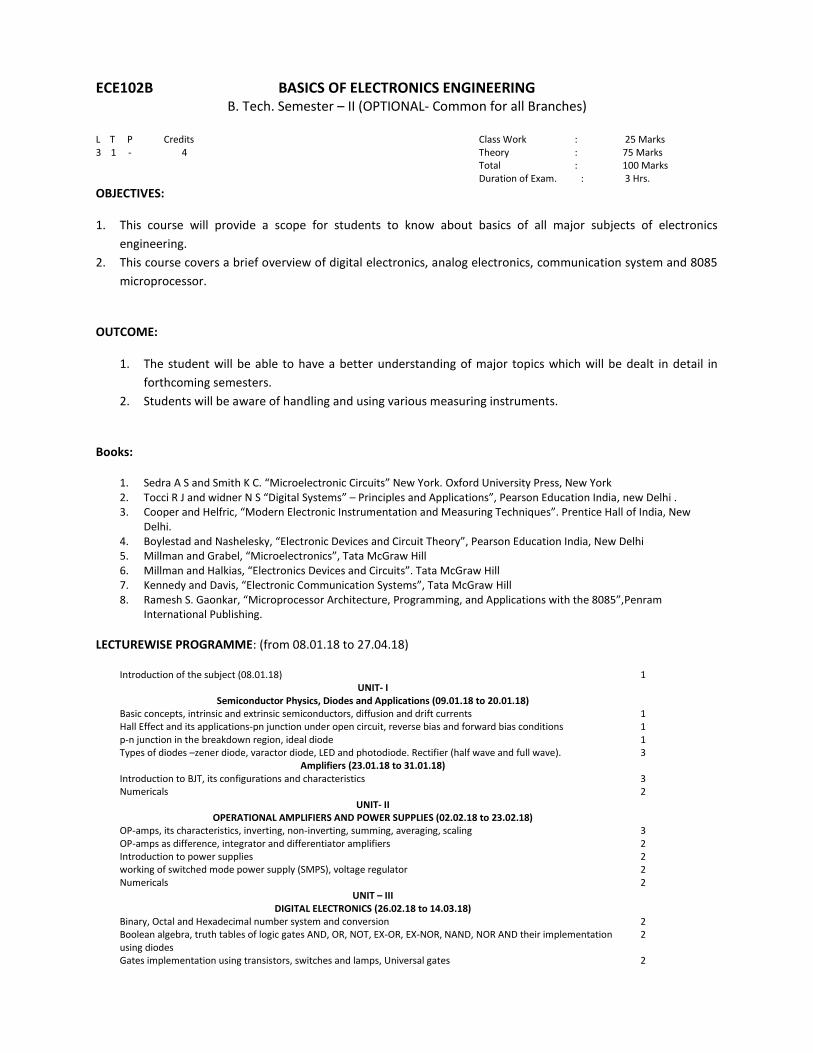
ECE102B BASICS OF ELECTRONICS ENGINEERING B. Tech. Semester – II (OPTIONAL- Common for all Branches) L T P Credits Class Work : 25 Marks 3 1 - 4 Theory : 75 Marks Total : 100 Marks Duration of Exam. : 3 Hrs. OBJECTIVES: 1. This course will provide a scope for students to know about basics of all major subjects of electronics engineering. 2. This course covers a brief overview of digital electronics, analog electronics, communication system and 8085 microprocessor. OUTCOME: 1. The student will be able to have a better understanding of major topics which will be dealt in detail in forthcoming semesters. 2. Students will be aware of handling and using various measuring instruments. Books: 1. Sedra A S and Smith K C. “Microelectronic Circuits” New York. Oxford University Press, New York 2. Tocci R J and widner N S “Digital Systems” – Principles and Applications”, Pearson Education India, new Delhi . 3. Cooper and Helfric, “Modern Electronic Instrumentation and Measuring Techniques”. Prentice Hall of India, New Delhi. 4. Boylestad and Nashelesky, “Electronic Devices and Circuit Theory”, Pearson Education India, New Delhi 5. Millman and Grabel, “Microelectronics”, Tata McGraw Hill 6. Millman and Halkias, “Electronics Devices and Circuits”. Tata McGraw Hill 7. Kennedy and Davis, “Electronic Communication Systems”, Tata McGraw Hill 8. Ramesh S. Gaonkar, “Microprocessor Architecture, Programming, and Applications with the 8085”,Penram International Publishing. LECTUREWISE PROGRAMME: (from 08.01.18 to 27.04.18) Introduction of the subject (08.01.18) 1 UNIT- I Semiconductor Physics, Diodes and Applications (09.01.18 to 20.01.18) Basic concepts, intrinsic and extrinsic semiconductors, diffusion and drift currents 1 Hall Effect and its applications-pn junction under open circuit, reverse bias and forward bias conditions 1 p-n junction in the breakdown region, ideal diode 1 Types of diodes –zener diode, varactor diode, LED and photodiode. Rectifier (half wave and full wave). 3 Amplifiers (23.01.18 to 31.01.18) Introduction to BJT, its configurations and characteristics 3 Numericals 2 UNIT- II OPERATIONAL AMPLIFIERS AND POWER SUPPLIES (02.02.18 to 23.02.18) OP-amps, its characteristics, inverting, non-inverting, summing, averaging, scaling 3 OP-amps as difference, integrator and differentiator amplifiers 2 Introduction to power supplies 2 working of switched mode power supply (SMPS), voltage regulator 2 Numericals 2 UNIT – III DIGITAL ELECTRONICS (26.02.18 to 14.03.18) Binary, Octal and Hexadecimal number system and conversion 2 Boolean algebra, truth tables of logic gates AND, OR, NOT, EX-OR, EX-NOR, NAND, NOR AND their implementation using diodes 2 Gates implementation using transistors, switches and lamps, Universal gates 2
Transcript of ECE102B BASICS OF ELECTRONICS …... using Basic gates and universal gates ... • Design and...
ECE102B BASICS OF ELECTRONICS ENGINEERING B. Tech. Semester – II (OPTIONAL- Common for all Branches)
L T P Credits Class Work : 25 Marks 3 1 - 4 Theory : 75 Marks
Total : 100 Marks Duration of Exam. : 3 Hrs.
OBJECTIVES:
1. This course will provide a scope for students to know about basics of all major subjects of electronics
engineering.
2. This course covers a brief overview of digital electronics, analog electronics, communication system and 8085
microprocessor.
OUTCOME:
1. The student will be able to have a better understanding of major topics which will be dealt in detail in
forthcoming semesters.
2. Students will be aware of handling and using various measuring instruments.
Books:
1. Sedra A S and Smith K C. “Microelectronic Circuits” New York. Oxford University Press, New York 2. Tocci R J and widner N S “Digital Systems” – Principles and Applications”, Pearson Education India, new Delhi . 3. Cooper and Helfric, “Modern Electronic Instrumentation and Measuring Techniques”. Prentice Hall of India, New
Delhi. 4. Boylestad and Nashelesky, “Electronic Devices and Circuit Theory”, Pearson Education India, New Delhi 5. Millman and Grabel, “Microelectronics”, Tata McGraw Hill 6. Millman and Halkias, “Electronics Devices and Circuits”. Tata McGraw Hill 7. Kennedy and Davis, “Electronic Communication Systems”, Tata McGraw Hill 8. Ramesh S. Gaonkar, “Microprocessor Architecture, Programming, and Applications with the 8085”,Penram
International Publishing.
LECTUREWISE PROGRAMME: (from 08.01.18 to 27.04.18)
Introduction of the subject (08.01.18) 1 UNIT- I
Semiconductor Physics, Diodes and Applications (09.01.18 to 20.01.18) Basic concepts, intrinsic and extrinsic semiconductors, diffusion and drift currents 1 Hall Effect and its applications-pn junction under open circuit, reverse bias and forward bias conditions 1 p-n junction in the breakdown region, ideal diode 1 Types of diodes –zener diode, varactor diode, LED and photodiode. Rectifier (half wave and full wave). 3
Amplifiers (23.01.18 to 31.01.18) Introduction to BJT, its configurations and characteristics 3 Numericals 2
UNIT- II OPERATIONAL AMPLIFIERS AND POWER SUPPLIES (02.02.18 to 23.02.18)
OP-amps, its characteristics, inverting, non-inverting, summing, averaging, scaling 3 OP-amps as difference, integrator and differentiator amplifiers 2 Introduction to power supplies 2 working of switched mode power supply (SMPS), voltage regulator 2 Numericals 2
UNIT – III DIGITAL ELECTRONICS (26.02.18 to 14.03.18)
Binary, Octal and Hexadecimal number system and conversion 2 Boolean algebra, truth tables of logic gates AND, OR, NOT, EX-OR, EX-NOR, NAND, NOR AND their implementation using diodes
2
Gates implementation using transistors, switches and lamps, Universal gates 2
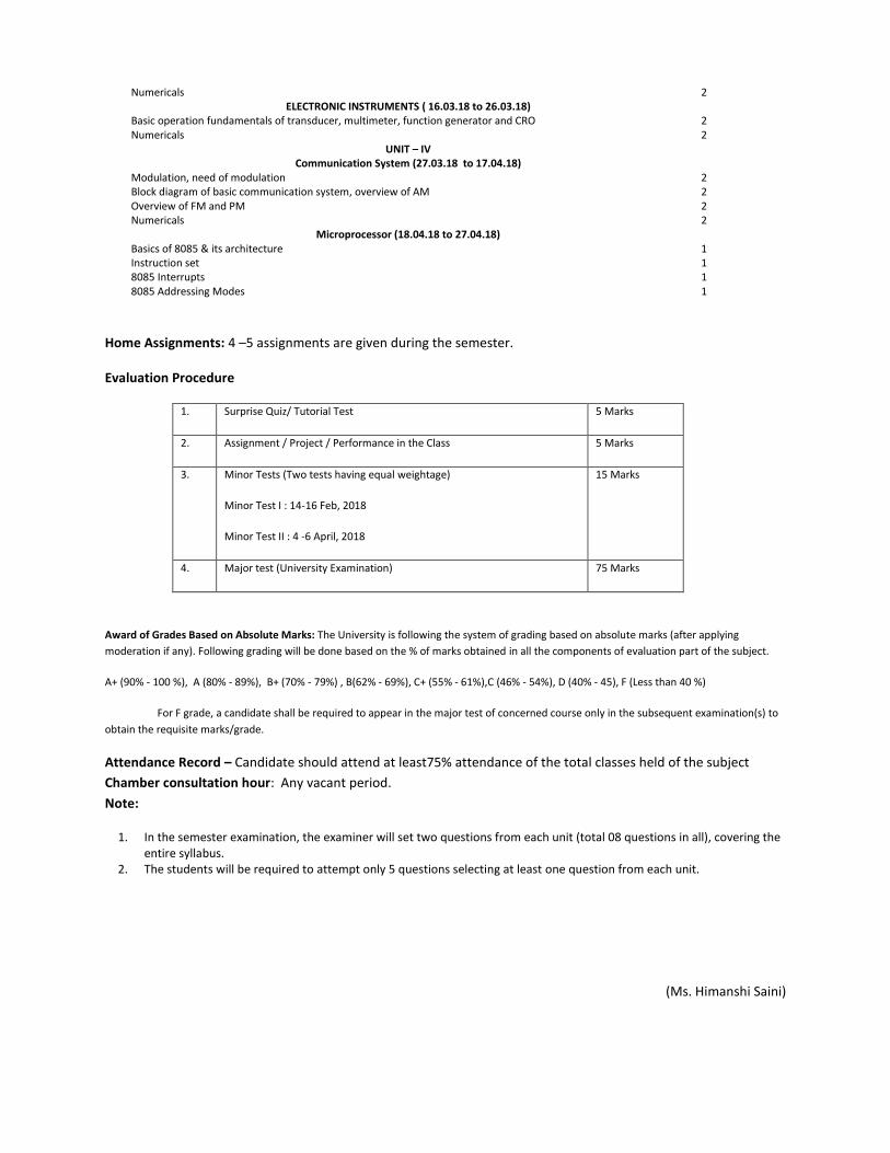
Numericals 2 ELECTRONIC INSTRUMENTS ( 16.03.18 to 26.03.18)
Basic operation fundamentals of transducer, multimeter, function generator and CRO 2 Numericals 2
UNIT – IV Communication System (27.03.18 to 17.04.18)
Modulation, need of modulation 2 Block diagram of basic communication system, overview of AM 2 Overview of FM and PM 2 Numericals 2
Microprocessor (18.04.18 to 27.04.18) Basics of 8085 & its architecture 1 Instruction set 1 8085 Interrupts 1 8085 Addressing Modes 1
Home Assignments: 4 –5 assignments are given during the semester.
Evaluation Procedure
1. Surprise Quiz/ Tutorial Test 5 Marks
2. Assignment / Project / Performance in the Class 5 Marks
3. Minor Tests (Two tests having equal weightage)
Minor Test I : 14-16 Feb, 2018
Minor Test II : 4 -6 April, 2018
15 Marks
4. Major test (University Examination) 75 Marks
Award of Grades Based on Absolute Marks: The University is following the system of grading based on absolute marks (after applying
moderation if any). Following grading will be done based on the % of marks obtained in all the components of evaluation part of the subject.
A+ (90% - 100 %), A (80% - 89%), B+ (70% - 79%) , B(62% - 69%), C+ (55% - 61%),C (46% - 54%), D (40% - 45), F (Less than 40 %)
For F grade, a candidate shall be required to appear in the major test of concerned course only in the subsequent examination(s) to
obtain the requisite marks/grade.
Attendance Record – Candidate should attend at least75% attendance of the total classes held of the subject
Chamber consultation hour: Any vacant period.
Note:
1. In the semester examination, the examiner will set two questions from each unit (total 08 questions in all), covering the entire syllabus.
2. The students will be required to attempt only 5 questions selecting at least one question from each unit.
(Ms. Himanshi Saini)
ECE204B DIGITAL CIRCUIT & SYSTEMS B. Tech. Semester –IV
L T P Credits Class Work : 25 Marks
3 1 - 4 Theory : 75 Marks
Total : 100 Marks
Duration of Exam. : 3 Hrs.
COURSE OBJECTIVES:
1. This course is designed to provide a comprehensive introduction to digital logic design leading to the ability to
understand number system representations, binary codes, binary arithmetic and Boolean algebra, its axioms and
theorems, and its relevance to digital logic design
2. Introduction to combinational circuits (such as Karnaugh maps), synchronous sequential logic and Asynchrnous
sequential logic.
3. Analyze and design simple systems composed of programmable logic, such as ROMs and PLAs.
COURSE OUTCOMES:
Upon completion of the subject, students will be able to
1. Understand binary number theory, Boolean algebra and binary codes.
2. Analyze and design combinational systems using standard gates and minimization methods (such as Karnaugh maps).
3. Analyze and design combinational systems composed of standard combinational modules, such as multiplexers and
decoders.
4. Implement simple synchronous sequential systems.
5. Analyze and design simple systems composed of programmable logic, such as ROMs and PLAs.
6. Perform basic arithmetic operations with signed integers represented in binary.
Reference Books:
1. Modern Digital Electronics (Edition III): R. P. Jain; TMH
2. Switching and Finite Automation Theory: Z.Kohavi; TMH
3. Introduction to Logic Design: MARKOVITZ ; TMH
4. Digital Design: Morris Mano; PHI.
5. Digital Electronics:Green; Pearson
LECTUREWISE PROGRAMME: (from 08.01.18 to 27.04.18)
Introduction of the subject (08.01.18)
1
UNIT-I (09.01.18 to 30.01.18 )
Number Systems and Codes, Revision of Boolean Algebra Introduction to Sets and their properties, Relations and Lattices
4
Minimization of switching functions: K Map (5 & 6 variables), Q M Method, VEM Method 3 Test/ quiz from minimization techniques
1
UNIT-II (01.02.18 to 28.02.18)
Logical design: using Basic gates and universal gates Logical design: using ICs ,High speed Adders
3
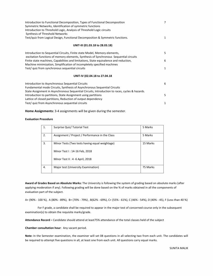
Introduction to Functional Decomposition, Types of Functional Decomposition Symmetric Networks, Identification of symmetric functions Introduction to Threshold Logic, Analysis of Threshold Logic circuits Synthesis of Threshold Networks
7
Test/quiz from Logical Design, Functional Decomposition & Symmetric functions.
1
UNIT-III (01.03.18 to 28.03.18)
Introduction to Sequential Circuits, Finite state Model, Memory elements, excitation functions of memory elements, Synthesis of Synchronous Sequential circuits
5
Finite state machines, Capabilities and limitations, State equivalence and reduction, Machine minimization, Simplification of incompletely specified machines
6
Test/ quiz from synchronous sequential circuits
1
UNIT-IV (02.04.18 to 27.04.18
Introduction to Asynchronous Sequential Circuits Fundamental mode Circuits, Synthesis of Asynchronous Sequential Circuits State Assignment in Asynchronous Sequential Circuits, Introduction to races, cycles & hazards.
6
Introduction to partitions, State Assignment using partitions Lattice of closed partitions, Reduction of output dependency
5
Test/ quiz from Asynchronous sequential circuits 1
Home Assignments: 3-4 assignments will be given during the semester.
Evaluation Procedure
1. Surprise Quiz/ Tutorial Test 5 Marks
2. Assignment / Project / Performance in the Class 5 Marks
3. Minor Tests (Two tests having equal weightage)
Minor Test I : 14-16 Feb, 2018
Minor Test II : 4 -6 April, 2018
15 Marks
4. Major test (University Examination) 75 Marks
Award of Grades Based on Absolute Marks: The University is following the system of grading based on absolute marks (after
applying moderation if any). Following grading will be done based on the % of marks obtained in all the components of
evaluation part of the subject.
A+ (90% - 100 %), A (80% - 89%), B+ (70% - 79%) , B(62% - 69%), C+ (55% - 61%), C (46% - 54%), D (40% - 45), F (Less than 40 %)
For F grade, a candidate shall be required to appear in the major test of concerned course only in the subsequent
examination(s) to obtain the requisite marks/grade.
Attendance Record – Candidate should attend at least75% attendance of the total classes held of the subject
Chamber consultation hour: Any vacant period.
Note: In the Semester examination, the examiner will set 08 questions in all selecting two from each unit. The candidates will
be required to attempt five questions in all, at least one from each unit. All questions carry equal marks.
SUNITA MALIK
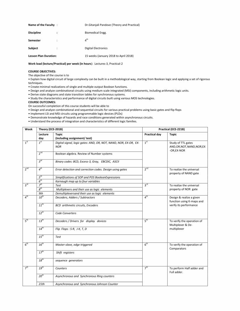
Name of the Faculty : Dr.Gitanjali Pandove (Theory and Practical)
Discipline : Biomedical Engg.
Semester : 4th
Subject : Digital Electronics
Lesson Plan Duration: 15 weeks (January 2018 to April 2018)
Work load (lecture/Practical) per week (in hours): Lectures-3, Practical-2
COURSE OBJECTIVES: The objective of the course is to • Explain how digital circuit of large complexity can be built in a methodological way, starting from Boolean logic and applying a set of rigorous techniques. • Create minimal realizations of single and multiple output Boolean functions. • Design and analyze combinational circuits using medium scale integrated (MSI) components, including arithmetic logic units. • Derive state diagrams and state transition tables for synchronous systems. • Study the characteristics and performance of digital circuits built using various MOS technologies. COURSE OUTCOMES: On successful completion of this course students will be able to • Design and analyze combinational and sequential circuits for various practical problems using basic gates and flip flops • Implement LSI and MSI circuits using programmable logic devices (PLDs) • Demonstrate knowledge of hazards and race conditions generated within asynchronous circuits. • Understand the process of integration and characteristics of different logic families.
Week Theory (ECE-201B) Practical (ECE-221B)
Lecture day
Topic (including assignment/ test)
Practical day Topic
1st 1st
Digital signal, logic gates: AND, OR, NOT, NAND, NOR, EX-OR, EX-NOR
1st Study of TTL gates AND,OR,NOT,NAND,NOR,EX-OR,EX-NOR
2nd
Boolean algebra. Review of Number systems
3rd
Binary codes: BCD, Excess-3, Gray, EBCDIC, ASCII
2nd
4th
Error detection and correction codes. Design using gates
2nd To realize the universal property of NAND gate
5th Simplifications of SOP and POS BooleanExpressions
6th Karnaugh map up to four variables
3rd
7th Test 3rd To realize the universal property of NOR gate 8th Multiplexers and their use as logic elements
9th Demultiplexersand their use as logic elements
4th
10th
Decoders, Adders / Subtractors 4th
Design & realize a given function using K-maps and verify its performance 11th
BCD arithmetic circuits, Encoders
12th
Code Converters
5th
13th
Decoders / Drivers for display devices 5th
To verify the operation of Multiplexer & De-multiplexer 14th
Flip Flops : S-R, J-K, T, D
15th
Test
6th
16th
Master-slave, edge triggered 6th
To verify the operation of Comparators
17th
Shift registers
18th
sequence generators
7th
19th
Counters 7th
To perform Half adder and Full adder.
20th
Asynchronous and Synchronous Ring counters
21th Asynchronous and Synchronous Johnson Counter
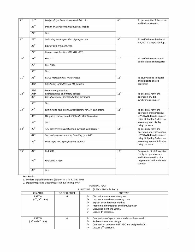
8th
22nd
Design of Synchronous sequential circuits 8th
To perform Half Substractor and Full substractor.
23rd
Design of Asynchronous sequential circuits
24th
Test
9th
25th
Switching mode operation of p-n junction 9th
To verify the truth table of S-R,J-K,T& D Type flip flop .
26th
Bipolar and MOS. devices
27th
Bipolar logic families: RTL, DTL, DCTL
10th
28th
HTL, TTL 10th
To verify the operation of bi-directional shift register
29th
ECL, MOS
30th
Test
11th
31th
CMOS logic families. Tristate logic 11th
To study analog to digital and digital to analog converter
32th
Interfacing of CMOS and TTL families
33th Memory organizations
12th
34th Characteristics of memory devices 12th
To design & verify the operation of 3 bit synchronous counter
35th
Classifications of semiconductors memories
36th
Test
13th
37th
Sample and hold circuit, specifications for D/A converters. 13th
To design & verify the operation of synchronous UP/DOWN decade counter using JK flip flop & derive a seven segment display using the same
38th
Weighted resistor and R -2 R ladder D/A Converters
39th
Test
14th
40th
A/D converters : Quantization, parallel -comparator 14th
To design & verify the operation of asynchronous UP/DOWN decade counter using JK flip flop & derive a seven segmenment display using the same
41th
Successive approximation, Counting type ADC
42th
Dual-slope ADC, specifications of ADCs
15th
44th
PLA, PAL 15th
Design a 4- bit shift register ,verify its operation and verify the operation of a ring counter and a Johnson counter
44th
FPGA and CPLDs
45th
Test
Text Books: 1. Modern Digital Electronics (Edition III) : R. P. Jain; TMH 2. Digital Integrated Electronics: Taub & Schilling; MGH
TUTORIAL PLAN
SUBJECT-DE (B.TECH BME 4th Sem.)
CHAPTER NO.OF LECTURE CONTENT
PART A (1ST , 2ND Unit)
6 Discussion on various binary No . Discussion on why to use Gray code Explain Error detection method Problem on multiplexer and demultiplexer Discussion on ff and Latch.. Discuss 1st sessional.
PART B ( 3rd and 4th Unit)
4 Comparision of synchronous and asynchronous ckt Problem on counter design Comparison between R-2R ADC and weighted ADC. Discuss 2nd sessional.
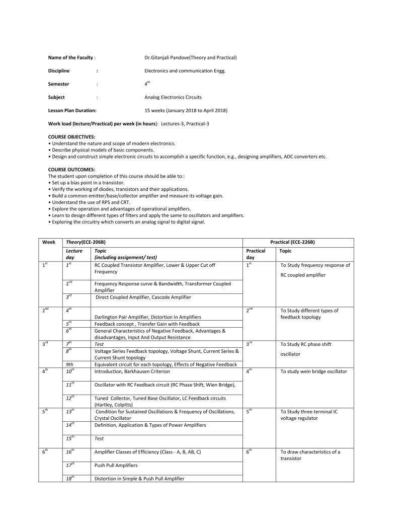
Name of the Faculty : Dr.Gitanjali Pandove(Theory and Practical)
Discipline : Electronics and communication Engg.
Semester : 4th
Subject : Analog Electronics Circuits
Lesson Plan Duration: 15 weeks (January 2018 to April 2018)
Work load (lecture/Practical) per week (in hours): Lectures-3, Practical-3
COURSE OBJECTIVES: • Understand the nature and scope of modern electronics. • Describe physical models of basic components. • Design and construct simple electronic circuits to accomplish a specific function, e.g., designing amplifiers, ADC converters etc. COURSE OUTCOMES: The student upon completion of this course should be able to:: • Set up a bias point in a transistor. • Verify the working of diodes, transistors and their applications. • Build a common emitter/base/collector amplifier and measure its voltage gain. • Understand the use of RPS and CRT. • Explore the operation and advantages of operational amplifiers. • Learn to design different types of filters and apply the same to oscillators and amplifiers. • Exploring the circuitry which converts an analog signal to digital signal.
Week Theory(ECE-206B) Practical (ECE-226B)
Lecture day
Topic (including assignment/ test)
Practical day
Topic
1st 1st
RC Coupled Transistor Amplifier, Lower & Upper Cut off Frequency
1st To Study frequency response of
RC coupled amplifier
2nd
Frequency Response curve & Bandwidth, Transformer Coupled Amplifier
3rd
Direct Coupled Amplifier, Cascode Amplifier
2nd
4th
Darlington Pair Amplifier, Distortion In Amplifiers
2nd To Study different types of feedback topology
5th Feedback concept , Transfer Gain with Feedback
6th General Characteristics of Negative Feedback, Advantages & disadvantages, Input And Output Resistance
3rd
7th Test 3rd To Study RC phase shift
oscillator 8th Voltage Series Feedback topology, Voltage Shunt, Current Series &
Current Shunt topology
9th Equivalent circuit for each topology, Effects of Negative Feedback
4th
10th
Introduction, Barkhausen Criterion 4th
To study wein bridge oscillator
11th
Oscillator with RC Feedback circuit (RC Phase Shift, Wien Bridge),
12th
Tuned Collector, Tuned Base Oscillator, LC Feedback circuits (Hartley, Colpitts)
5th
13th
Condition for Sustained Oscillations & Frequency of Oscillations, Crystal Oscillator
5th
To Study three terminal IC voltage regulator
14th
Definition, Application & Types of Power Amplifiers
15th
Test
6th
16th
Amplifier Classes of Efficiency (Class - A, B, AB, C) 6th
To draw characteristics of a transistor
17th
Push Pull Amplifiers
18th Distortion in Simple & Push Pull Amplifier
7th
19th
Complementary Push Pull Amplifier, Integrated Circuit Power Amplifier
7th
To study CE amplifier and
calculate its gain.
20th
Introduction to MOSFET & CLASS D Power Amplifier
21th
Voltage Regulation, Basic Series Regulators, Basic Switching Regulators
8th
22nd
Basic Shunt Regulators, Power Supply Parameters 8th
To study 555 timer as a square wave generator
23rd
Step up Configuration , Step down Configuration
24th
Test
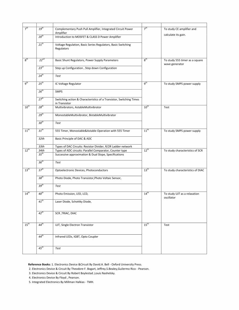
9th
25th
IC Voltage Regulator 9th
To study SMPS power supply
26th
SMPS
27th
Switching action & Characteristics of a Transistor, Switching Times in Transistor
10th
28th
Multivibrators, AstableMultivibrator 10th
Test
29th
MonostableMultivibrator, BistableMultivibrator
30th
Test
11th
31th
555 Timer, Monostable&Astable Operation with 555 Timer 11th
To study SMPS power supply
32th
Basic Principle of DAC & ADC
33th Types of DAC Circuits: Resistor Divider, R/2R Ladder network
12th
34th Types of ADC circuits: Parallel Comparator, Counter type 12th
To study characteristics of SCR
35th
Successive approximation & Dual Slope, Specifications
36th
Test
13th
37th
Optoelectronic Devices, Photoconductors 13th
To study characteristics of DIAC
38th
Photo Diode, Photo Transistor,Photo Voltaic Sensor,
39th
Test
14th
40th
Photo Emission, LED, LCD, 14th
To study UJT as a relaxation oscillator
41th
Laser Diode, Schottky Diode,
42th
SCR ,TRIAC, DIAC
15th
44th
UJT, Single Electron Transistor 15th
Test
44th
Infrared LEDs, IGBT, Opto Coupler
45th
Test
Reference Books: 1. Electronics Device &Circuit By David.A. Bell - Oxford University Press.
2. Electronics Device & Circuit By Theodore F. Bogart, Jeffrey.S.Bealey,Guilermo Rico - Pearson.
3. Electronics Device & Circuit By Robert Boylestad ,Louis Nashelsky.
4. Electronics Device By Floyd , Pearson.
5. Integrated Electronics By Millman Halkias - TMH.
6. Electronics Device & Circuit By Sanjeev Gupta.
7. Electronics Device & Circuit By I. J. Nagrath - PHI
8. Electronic Principles By Albert Malvino
ECE208B POWER ELECTRONICS
B. Tech. Semester –IV (ECE, common with 6th Sem. AEI)
L T P Credits Class Work: 25
3 1 - 04 Theory Marks: 75
Marks Total : 100
Duration of Exams: 3 Hours
OBJECTIVES:
1.To introduce the theory and applications of power electronics systems for high efficiency, renewable and energy
saving conversion systems.
2.To characterize different power electronics switches, drivers and selection of components for different
applications
3. To develop students with an understanding of the switching behavior and design of power electronics circuits
such as DC/DC, AC/DC, DC/AC and AC/AC converters.
OUTCOMES:
1.An ability to understand basic operation of various power semiconductor devices and passive components.
2.An ability to understand the basic principle of switching circuits.
3. An ability to analyze and design an AC/DC rectifier circuit.
4. An ability to analyze and design DC/DC converter circuits.
5. An ability to analyze DC/AC inverter circuit.
6. An ability to understand the role power electronics play in the improvement of energy usage efficiency and the
development of renewable energy technologies
Text Books :
1.P.SBimbhra : Power Electronics, Khanna Publisher
2. MuhamedH.Rashid : Power Electronics Circuits, Devices and Applications, PHI.
3. Singh And Kanchandani : Power Electronics, TMH.1.
Reference Books:
1.Sen : Power Electronics, TMH .
2. Dubey :Thyristorised Power Controllers, Wiley Eastern .
3. Vithayathil : Power Electronics – Principles And Applications, McGraw-Hill.
4. Lander : Power Electronics, McGraw-Hill.
LECTUREWISE PROGRAMME : (from 15.01.18 to 27.04.18)
Introduction of the subject (15.01.18) 1
UNIT- I
POWER SEMICONDUCTOR DIODES AND TRANSISTORS: (17.01.18 to 23.01.18)
Characteristics of Power Diodes, Types of Power Diodes Power Transistors, Power MOSFET Insulated Gate Bipolar Transistors (IGBT), MOS Controlled Thyristors.
THYRISTORS: (24.01.18 to 16.02.18)
Terminal Characteristics of Thyristors Thyristor Turn ON Methods, Switching Characteristics of Thyristors Thyristors Gate Characteristics, Two Transistor Model of a Thyristor Thyristor Ratings, Thyristors Protection, Heating Cooling and Mounting of Thyristors, Series and Parallel Operation of Thyristors Programmable Unijunction Transistors(PUT),Silicon Unilateral Switch(SUS) Silicon Controlled Switch(SCS) ,Light Activated Thyristors Static Induction Thyristors, Diac, Triac Asymmetric Thyristors, Reverse Conducting Thyristors Firing Circuits for Thyristors, Pulse Transformer in Firing Circuits Triac Firing Circuit
1 1 2 1 1 1 1 1 1 1 1 1 1 1 1 1
UNIT- II
THYRISTORS COMMUTATION TECHNIQUES:(19.02.18 to 28.02.18)
Class A Commutation (Load Commutation), Class B Commutation (Resonant Pulse Commutation), Class C Commutation (Complementary Commutation), Class D Commutation (Impulse Commutation), Class E Commutation (External Pulse Commutation), Class F Commutation (Line Commutation)
1 1 1 1
PHASE CONTROLLED RECTIFIER:: (2.03.18 to 16.03.18)
Principle of Phase Control ,Full Wave Controlled Converters Single Phase Full Wave Converter, Single Phase Two Pulse Converter with Discontinuous Load Current, Three Phase Converter Systems Using Diodes ,Three Phase Thyristor Converter Circuits, Effect of Source Impedance on Performance of Converter, Dual Converters.
1 2 1 1
UNIT- III CHOPPERS (20.03.18 to 26.03.18)
Principle of Chopper Operation, Control Strategies, Step Up Choppers, Types of Chopper Circuits, Steady State Time Domain Analysis of Type A Chopper, Thyristor Chopper Circuits, Multiphase Choppers.
1 1 2
INVERTERS(27.03.18 to 10.04.18)
Single Phase Voltage Source Inverter: Operating Principle ,Force Commutated Thyristor Inverters, Three Phase Bride Inverter, Voltage Control in Single Phase Inverter, Pulse Width Modulated Inverter, Reduction of Harmonics in the Inverter Output Voltage, Current Source Inverters, Series Inverters, Single Phase Parallel Inverter.
1 2 2
UNIT- IV
AC VOLTAGE CONTROLLER AND CYCLOCONVERTERS:. (11.04.18 to 19.04.18)
Types of AC Voltage Controller, Integral Cycle Control, Single Phase Voltage Controllers Sequence Control of AC Voltage Controller. Principle of Cycloconverter Operation, Three Phase Half Wave Cycloconverter, Output Voltage Equation for Cycloconverter Load Commutated Cycloconverter.
2 2 1 1
APPLICATIONS(20.04.18 to 27.04.18)
Switched Mode Power Supply(SMPS),Uninterruptible Power Supplies, High Voltage DC Transmission, Static Switches, Static Circuit Breakers, Solid State Relays.
1 1 1
Home Assignments :4 –5 assignments are given during the semester.
Evaluation Procedure
1. Surprise Quiz/ Tutorial Test 5 Marks
2. Assignment / Project / Performance in the Class 5 Marks
3. Minor Tests (Two tests having equal weightage)
Minor Test I : 14-16 Feb, 2018
Minor Test II : 4 -6 April, 2018
15 Marks
4. Major test (University Examination) 75 Marks
Award of Grades Based on Absolute Marks: The University is following the system of grading based on absolute marks (after applying
moderation if any). Following grading will be done based on the % of marks obtained in all the components of evaluation part of the subject.
A+ (90% - 100 %), A (80% - 89%), B+ (70% - 79%) , B(62% - 69%), C+ (55% - 61%),C (46% - 54%), D (40% - 45), F (Less than 40 %)
For F grade, a candidate shallbe required to appear in the major test of concerned course only in the subsequent examination(s) to
obtain the requisite marks/grade.
Attendance Record – Candidate should attend at least75% attendance of the total classes held of the subject
Chamber consultation hour: Any vacant period.
Note:
1. In the semester examination, the examiner will set 08 questions in all selecting two from each unit (1 & 2 from unit I, 3 & 4 from unit II, 5 &6 from unit III and 7 & 8 from unit IV). The students will be required to attempt only 5 questions selecting at least one question from each unit. All questions will carry equal marks.
2. The use of scientific calculator will be allowed in the examination. However, programmable calculator and cellular phone will not be allowed.
(SALONI RAI)
ECE210B COMMUNICATION SYSTEMS
LECTUREWISE PROGRAMME: (from 08.01.18 to 27.04.18)
UNIT I
INTRODUCTION TO COMMUNICATION SYSTEM: (8.01.2018- 25.01.2018) Modulation, Demodulation, Radio Frequency Spectrum, Signals & their classification, Limitations & Advantages of a Communication System, Comparison of Analog & Digital Communication Systems, Historical Perspective, Modes & Medias of Communication. ( 4-5 Lectures) NOISE: Sources of Noise, External & Internal Noise, Noise Calculations, Noise Figure, Noise Figure Calculation, Noise Temperature, Noise in Communication Systems, Band Pass Noise Model, Cascaded States & its Noise Figure Calculation, Signal in presence of Noise, Pre-Emphasis & De-Emphasis, Noise Quieting Effect, Capture Effect, Noise in Modulation Systems. (5-6 Lectures)
UNIT II
LINEAR MODULATION: (29.01.2018- 27.02.2018) (AM) Basic definition & derivation for Modulation & Modulation Index, Modulation & Demodulation of AM, Suppressed Carrier Modulation, Quadrature Amplitude Modulation, SSB-SC, DSB-SC, VSB Modulation & Demodulation, Comparison of various AM Systems, Generation of AM waves. ( 5-6 Lectures) ANGLE MODULATION: Basic definition & derivation for Modulation & Modulation Index, Generation of FM waves, Comparison between PM & FM, Frequency Spectrum of FM, B.W. & required spectra, Types of FM, vector representation of FM, Universal Curve, Multiple FM, Demodulation of FM waves, Demodulation of PM waves, Comparison between AM & FM. ( 7-8 Lectures)
UNIT III
TRANSMITTERS & RECEIVERS: (28.02.2018 – 22.03.2018) Classification of Radio Transmitters, Basic Block Diagram of Radio Transmitter, Effect of Feedback on operation of Transmitter, Radio Telephone Transmitters, Privacy Device in Radio Telephony, FM Transmitter using Reactance Modulator, Armstrong FM Transmitter, Radio Receivers, Classification, TRF Receiver, Super Heterodyne Receiver, Image Rejection & Double Spotting, Choice of IF, Tracking & Alignment of Receivers, AGC. (5-6) Lectures PROBABILITY THEORY & RANDOM PROCESSES: Probability, Properties, Conditional Probability, Random Variables, CDF, PDF, Uniform Distribution, Random or Stochastic Process, Ergodic Process, PSD, Properties of PSD, Correlation Function. (3-4 Lectures)
UNIT IV
PULSE ANALOG MODULATION: ( 26.03.2018 – 27.04.2018) Sampling theory, TDM, FDM, PAM, PWM, PPM, Modulation & Demodulation techniques of above all. (5-6 Lectures) PULSE DIGITAL MODULATION: Elements of Pulse Code Modulation, Noise in PCM Systems, Bandwidth of PCM Systems, Measure of Information, Channel Capacity, Channel Capacity of PCM System, Differential Pulse Code Modulation (DPCM). Delta Modulation (DM) (5-6 Lectures) Home Assignments :4 –5 assignments are given during the semester.
Evaluation Procedure
1. Surprise Quiz/ Tutorial Test 5 Marks
2. Assignment / Project / Performance in the Class 5 Marks
3. Minor Tests (Two tests having equal weightage)
Minor Test I : 14-16 Feb, 2018
Minor Test II : 4 -6 April, 2018
15 Marks
4. Major test (University Examination) 75 Marks
Award of Grades Based on Absolute Marks: The University is following the system of grading based on absolute marks (after
applying moderation if any). Following grading will be done based on the % of marks obtained in all the components of
evaluation part of the subject.
A+ (90% - 100 %), A (80% - 89%), B+ (70% - 79%) , B(62% - 69%), C+ (55% - 61%),C (46% - 54%), D (40% - 45), F (Less than 40 %)
For F grade, a candidate shallbe required to appear in the major test of concerned course only in the subsequent
examination(s) to obtain the requisite marks/grade.
Attendance Record – Candidate should attend at least75% attendance of the total classes held of the subject
Chamber consultation hour: Any vacant period.
Reference Books: 1. Communication Systems By Manoj Duhan – I. K. International 2. Electronic Communication Systems By Kennedy – TMH 3. Communication Systems By Singh & Sapre – TMH 4. Electronic Communication, By Roody Coolen – Pearson 5. Analog Communication By P. Chakarbarti – DR & Co. 6. Communication Systems By Simon Haykins – Wiley
NOTE: In the Semester examination, the examiner will set 08 questions in all selecting two from each unit. The candidates will be required to attempt five questions in all, at least one from each unit. All questions carry equal marks.
ECE212B FIELD AND WAVES
L T P Credits Sessional Marks: 25
3 1 - 04 Theory Marks: 75
Duration of Exams: 3 Hours
OBJECTIVES:
1. To acquire the knowledge on basic electromagnetic field theory and specially Maxwell’s equations, Boundary
conditions for fields at different material interfaces and plane waves.
2. Student will learn scientific, mathematical and engineering principle that enable to understand forces, field
and waves.
OUTCOME:
1. Gain a comprehensive knowledge on basic concepts of static & time varying Electric and Magnetic fields.
2. Understand about the Maxwell’s Equations and its applications.
Text Books :
1. Electro-magnetic Waves and Radiating System : Jordan & Balmain, PHI.
2. Antenna & Wave Propagation: K.D Prasad, Satya Prakashan.
3. Field and Wave Electromagnetics: David K.Cheng, Pearson,Second edition.
Reference Books:
1. Engineering Electromagnetics: Umran S.Inan & Aziz S. Inan, Pearson
2. Engineering Electromagnetics : Hayt; TMH
3. Electro-Magnetics : Krauss J.DF; Mc Graw Hill.
LECTUREWISE PROGRAMME : (from 15.01.18 to 27.04.18)
Introduction of the subject (16.01.18)
1
UNIT- I INTRODUCTION TO ELECTROSTATIC: (17.01.18 to 2.02.18)
Coulomb’s Law Of Electrostatic Force 1 Electric Field Intensity 1 Electric Potential, Electric Charge Density 2 Field of A Finite Line Of Charge, Field Potential of an Infinite Line Of Charge Electric Potential Difference, Electric Dipole, Electric Flux Density Numericals and problems
2 1 1
GAUSS LAW AND IT’S APPLICATION (06.02.18 to 13.02.18) Gauss Law, Application of Gauss Law 1
Laplace Equation, Solution of Laplace Equation in Rectangular And Cartesian Coordinates Uniqueness Theorem of Electrostatic Field Solutions
1 1
Methods of Electrostatic Images Electrostatic Energy, Capacitance Numericals
1 1 1
UNIT- II MAGNOSTATICS (20.02.18 to 2.03.18)
Introduction, Faraday Induction Law Magnetic Effect on Current Carrying Conductor Magnetic Flux
1 1 1
Magnetic Flux Density 1 Biot-Savart’s Law, Ampere’s Law of Force 1 Numericals 1
ELECTROMAGNETIC INDUCTION: (6.03.18 to 16.03.18) Magnetic Field of A Solenoid, Magnetic Field In Vector Notations, Magnetic Field Intensity Magnetic Flux Density outside and inside an Infinitely Long Cylinder Containing Uniform Current Density Magnetic Vector Potential, Energy Stored In A Magnetic Field Energy Density In A Magnetic Field
2 1 2 1
UNIT- III ELECTROMAGNETIC WAVE (20.03.18 to 23.03.18)
Introduction, Displacement Current Mawell’s Equations: In Free Space, Differential Form And Integra Form Physical Interpretations Of Maxwell’s Field Equations, Boundary Conditions
1
Numericals 1 1
WAVE EQUATIONS (27.03.18 to 30.03.18) 1 Electromagnetic Wave In Homogeneous Medium, Wave Equation, Plane Wave And Uniform Plane Wave Electromagnetic Wave Equations, Wave Propagation In Conducting Medium, Polarization
1
UNIT- IV
TRANSMISSION LINES (10.04.18 to 14.04.18) Introduction, Basic Principles Of Transmission Lines, Equivalent Circuit Representation, General Transmission line. Wave Characteristics on Finite Transmission Lines, Transients on Transmission lines
2 2
MATCHING NETWORKS (17.04.18 to 27.04.18) Primary Constant, Voltage And Current calculations Characteristic Impedance, Open And Short Circuit Lines Reflection Coefficient, VSWR, Smith’s Chart And Its Applications. Numericals
1 2 2 1
Home Assignments :4 –5 assignments are given during the semester.
Evaluation Procedure
1. Surprise Quiz/ Tutorial Test 5 Marks
2. Assignment / Project / Performance in the Class 5 Marks
3. Minor Tests (Two tests having equal weightage)
Minor Test I : 14-16 Feb, 2018
Minor Test II : 4 -6 April, 2018
15 Marks
4. Major test (University Examination) 75 Marks
Award of Grades Based on Absolute Marks: The University is following the system of grading based on absolute marks (after applying
moderation if any). Following grading will be done based on the % of marks obtained in all the components of evaluation part of the subject.
A+ (90% - 100 %), A (80% - 89%), B+ (70% - 79%) , B(62% - 69%), C+ (55% - 61%),C (46% - 54%), D (40% - 45), F (Less than 40 %)
For F grade, a candidate shallbe required to appear in the major test of concerned course only in the subsequent examination(s) to
obtain the requisite marks/grade.
Attendance Record – Candidate should attend at least75% attendance of the total classes held of the subject
Chamber consultation hour: Any vacant period.
Note:
3. In the semester examination, the examiner will set 08 questions in all selecting two from each unit (1 & 2 from unit I, 3 & 4 from unit II, 5 &6 from unit III and 7 & 8 from unit IV). The students will be required to attempt only 5 questions selecting at least one question from each unit. All questions will carry equal marks.
4. The use of scientific calculator will be allowed in the examination. However, programmable calculator and cellular phone will not be allowed.
(SWEETY)
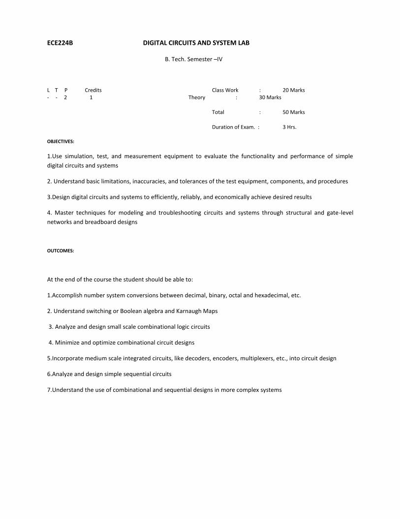
ECE224B DIGITAL CIRCUITS AND SYSTEM LAB
B. Tech. Semester –IV
L T P Credits Class Work : 20 Marks - - 2 1 Theory : 30 Marks
Total : 50 Marks
Duration of Exam. : 3 Hrs.
OBJECTIVES:
1.Use simulation, test, and measurement equipment to evaluate the functionality and performance of simple
digital circuits and systems
2. Understand basic limitations, inaccuracies, and tolerances of the test equipment, components, and procedures
3.Design digital circuits and systems to efficiently, reliably, and economically achieve desired results
4. Master techniques for modeling and troubleshooting circuits and systems through structural and gate-level
networks and breadboard designs
OUTCOMES:
At the end of the course the student should be able to:
1.Accomplish number system conversions between decimal, binary, octal and hexadecimal, etc.
2. Understand switching or Boolean algebra and Karnaugh Maps
3. Analyze and design small scale combinational logic circuits
4. Minimize and optimize combinational circuit designs
5.Incorporate medium scale integrated circuits, like decoders, encoders, multiplexers, etc., into circuit design
6.Analyze and design simple sequential circuits
7.Understand the use of combinational and sequential designs in more complex systems
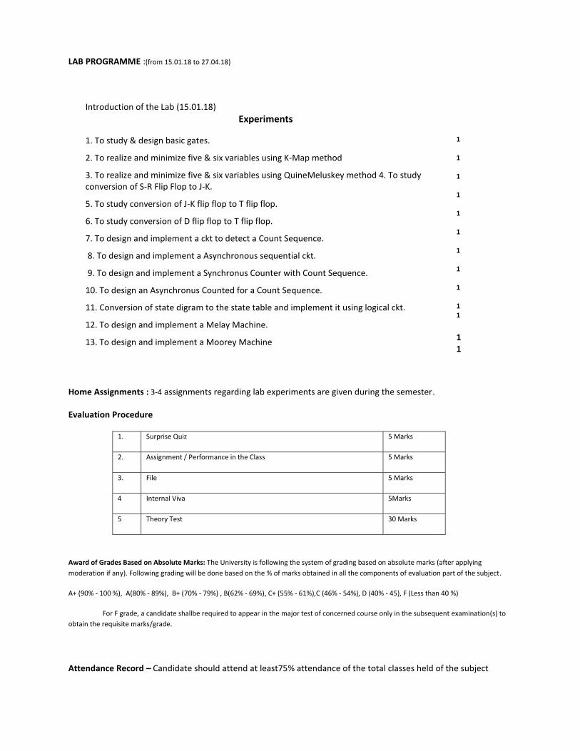
LAB PROGRAMME :(from 15.01.18 to 27.04.18)
Introduction of the Lab (15.01.18)
Experiments
1. To study & design basic gates.
2. To realize and minimize five & six variables using K-Map method
3. To realize and minimize five & six variables using QuineMeluskey method 4. To study conversion of S-R Flip Flop to J-K.
5. To study conversion of J-K flip flop to T flip flop.
6. To study conversion of D flip flop to T flip flop.
7. To design and implement a ckt to detect a Count Sequence.
8. To design and implement a Asynchronous sequential ckt.
9. To design and implement a Synchronus Counter with Count Sequence.
10. To design an Asynchronus Counted for a Count Sequence.
11. Conversion of state digram to the state table and implement it using logical ckt.
12. To design and implement a Melay Machine.
13. To design and implement a Moorey Machine
1 1 1 1 1 1 1 1 1 1 1
1 1
Home Assignments : 3-4 assignments regarding lab experiments are given during the semester.
Evaluation Procedure
1. Surprise Quiz 5 Marks
2. Assignment / Performance in the Class 5 Marks
3. File 5 Marks
4 Internal Viva 5Marks
5 Theory Test 30 Marks
Award of Grades Based on Absolute Marks: The University is following the system of grading based on absolute marks (after applying
moderation if any). Following grading will be done based on the % of marks obtained in all the components of evaluation part of the subject.
A+ (90% - 100 %), A(80% - 89%), B+ (70% - 79%) , B(62% - 69%), C+ (55% - 61%),C (46% - 54%), D (40% - 45), F (Less than 40 %)
For F grade, a candidate shallbe required to appear in the major test of concerned course only in the subsequent examination(s) to
obtain the requisite marks/grade.
Attendance Record – Candidate should attend at least75% attendance of the total classes held of the subject
Chamber consultation hour: Any vacant period.
NOTE:-
1 Total ten experiments are to be performed in the semester.
2 At least seven experiments should be performed from the above list. Remaining three experiments should be
performed as designed and set by the concerned institution as per the scope of the syllabus.
(SaloniRai)
ECE228B POWER ELECTRONICS LAB
B. Tech. Semester –IV (ECE, common with 6th Sem. AEI)
L T P Credits Class Work : 20 Marks - - 2 1 Theory : 30 Marks
Total : 50 Marks
Duration of Exam. : 3 Hrs.
OBJECTIVES:
1.To provide an in-depth knowledge about characteristics of SCR, UJT
2.To implement various configurations of full wave rectifier circuit
OUTCOME:
1.The student upon completion of this course should be able to: Analyze various characteristics of SCR at various
load conditions.
2.Student will have a better understanding of UJT, TRIAC and DIAC features
3.Student will be able to characterize rectifier circuits
LAB PROGRAMME :(from 15.01.18 to 27.04.18)
Introduction of the Lab (15.01.18)
Experiments
1.To study Steady-state characteristics of SCR by plotting graph between voltage and current of Thyristers.
2. To Study R and RC Triggering Circuit for SCR.
3. To study UJT as Relaxation Oscillator.
4. To study SCR Half Wave and Full Wave Bridge Controlled Rectifier-Output characteristics.
5. To study 1-Phase Full Wave Bridge Controlled Rectifier using SCR and UJT with R and R-L Load and observe its input/output characteristics with and without free wheeling (commutating ) diode.
6 To study three Phase Full-Wave Uncontrolled Rectifier Operation with R and R-L Load and Observe its input/output Characteristics.
7. To study single Phase Cycloconvener output characteristics.
8. To study Series operation of SCR’s.
1 1 1 1 1 1 1 1
9. To study Parallel operation of SCR’s.
10. To study Speed Control of DC motor using SCR’s.
11. To study Lamp-Dimmer Using Diac&Triac With Lamp Load.
1 1
1
Home Assignments : 3-4 assignments regarding lab experiments are given during the semester.
Evaluation Procedure
1. Surprise Quiz 5 Marks
2. Assignment / Performance in the Class 5 Marks
3. File 5 Marks
4 Internal Viva 5Marks
5 Theory Test 30 Marks
Award of Grades Based on Absolute Marks: The University is following the system of grading based on absolute marks (after applying
moderation if any). Following grading will be done based on the % of marks obtained in all the components of evaluation part of the subject.
A+ (90% - 100 %), A(80% - 89%), B+ (70% - 79%) , B(62% - 69%), C+ (55% - 61%),C (46% - 54%), D (40% - 45), F (Less than 40 %)
For F grade, a candidate shallbe required to appear in the major test of concerned course only in the subsequent examination(s) to
obtain the requisite marks/grade.
Attendance Record – Candidate should attend at least75% attendance of the total classes held of the subject
Chamber consultation hour: Any vacant period.
NOTE:-
1 Total ten experiments are to be performed in the semester.
2 At least seven experiments should be performed from the above list. Remaining three experiments should be
performed as designed and set by the concerned institution as per the scope of the syllabus.
(SaloniRai)
ECE302B MICROWAVE AND RADAR ENGINEERING
L T P Credits Sessional Marks: 25
3 1 - 04 Theory Marks: 75
Duration of Exams: 3 Hours
OBJECTIVES:
1. To make students understand the working principles of various devices operating at microwave frequencies.
2. To introduce students, to the basics of radar systems
3. To introduce the students, to the basics of microwave devices and components.
OUTCOME:
1. The student will gain complete knowledge about microwave devices such as Amplifiers, Oscillators 2. The students will have knowledge of microwave Measurement techniques. 3. The students will become aware of various radar frequencies and radar classifications.
Text Books :
1. Foundations for Microwave Engineering: R.E.Collin, MGH 2. Introduction to Radar Systems: Merrill I. Skolnik, MGH
Reference Books:
1. Radar Principles, Technology, Applications: Byron Edde, Pearson Education 2. Microwave Devices and Circuit: Samuel Liao, PHI. 3. Elements of Microwave Engineering : R.Chatterjee, EWP
LECTUREWISE PROGRAMME : (from 15.01.18 to 27.04.18)
Introduction of the subject (16.01.18) 1
UNIT- I
INTRODUCTION TO MICROWAVES: (17.01.18 to 2.02.18) Characteristic features- advantages and applications 1 Waveguides- Basic concepts and properties, Comparison of Waveguide with transmission lines 1 TEM mode in rectangular waveguide, planar transmission lines 1 Propagation in TE & TM mode, Rectangular waveguide Introduction to circular waveguides Numericals
2 1 1
MICROWAVE COMPONENTS (06.02.18 to 13.02.18) Tees Hybrid Ring , Directional Couplers, Phase shifter Attenuators, Mixers & detectors, Matched load
1 1 1
Cavity resonators Isolators, Circulators Numericals
1 1 1
UNIT- II
MICROWAVE TUBES (20.02.18 to 2.03.18) Limitations of conventional tubes Construction, operation , properties and applications of Klystron amplifier Reflex Klystron
1 1 1
TWT, BWO 1 Magnetron, Crossed field amplifiers. 1 Numericals 1
MICROWAVE SOLID STATE DEVICES: (6.03.18 to 16.03.18) Principle of operation and applications of Varactor diode, Tunnel diode Schottky diode, GUNN diode IMPATT, TRAPATT and PIN diodes Numericals
1 1 2 1
UNIT- III MICROWAVE MEASUREMENTS (20.03.18 to 23.03.18)
Measurement of Frequency, Power, VSWR Wavelength & Impedance
1
Numericals 1 1
RADAR FUNDAMENTALS (27.03.18 to 30.03.18) 1 Introduction, RADAR principles, development, frequencies block diagram and operation and applications.
1
UNIT- IV
RADAR EQUATION (10.04.18 to 13.04.18) Simple form of RADAR equation, Prediction of Range Performance, Minimum detectable signal Pulse repletion frequency & range ambiguities, system losses, propagation effects.
1 2
RADAR SYSTEMS (17.04.18 to 27.04.18) Block Diagram and operation of CW , Frequency Modulated RADAR MTI & Pulsed Doppler RADAR The Doppler effect, blind speed, Applications. Numericals
1 1 1 3
Home Assignments :4 –5 assignments are given during the semester.
Evaluation Procedure
1. Surprise Quiz/ Tutorial Test 5 Marks
2. Assignment / Project / Performance in the Class 5 Marks
3. Minor Tests (Two tests having equal weightage)
Minor Test I : 14-16 Feb, 2018
Minor Test II : 4 -6 April, 2018
15 Marks
4. Major test (University Examination) 75 Marks
Award of Grades Based on Absolute Marks: The University is following the system of grading based on absolute marks (after applying
moderation if any). Following grading will be done based on the % of marks obtained in all the components of evaluation part of the subject.
A+ (90% - 100 %), A (80% - 89%), B+ (70% - 79%) , B(62% - 69%), C+ (55% - 61%),C (46% - 54%), D (40% - 45), F (Less than 40 %)
For F grade, a candidate shallbe required to appear in the major test of concerned course only in the subsequent examination(s) to
obtain the requisite marks/grade.
Attendance Record – Candidate should attend at least75% attendance of the total classes held of the subject
Chamber consultation hour: Any vacant period.
Note:
1. In the semester examination, the examiner will set 08 questions in all selecting two from each unit (1 & 2 from unit I, 3 & 4 from unit II, 5 &6 from unit III and 7 & 8 from unit IV). The students will be required to attempt only 5 questions selecting at least one question from each unit. All questions will carry equal marks.
2. The use of scientific calculator will be allowed in the examination. However, programmable calculator and cellular phone will not be allowed.
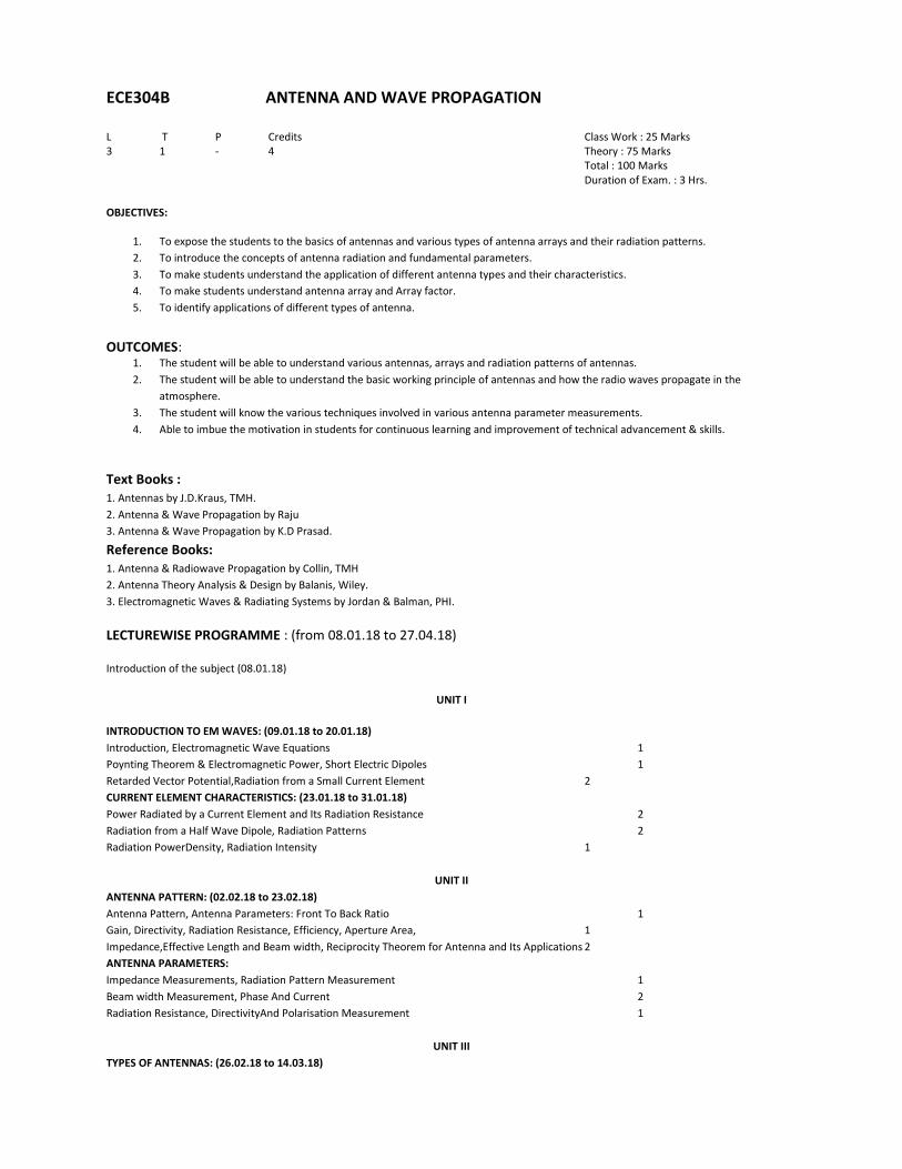
ECE304B ANTENNA AND WAVE PROPAGATION L T P Credits Class Work : 25 Marks 3 1 - 4 Theory : 75 Marks
Total : 100 Marks Duration of Exam. : 3 Hrs.
OBJECTIVES:
1. To expose the students to the basics of antennas and various types of antenna arrays and their radiation patterns.
2. To introduce the concepts of antenna radiation and fundamental parameters.
3. To make students understand the application of different antenna types and their characteristics.
4. To make students understand antenna array and Array factor.
5. To identify applications of different types of antenna.
OUTCOMES: 1. The student will be able to understand various antennas, arrays and radiation patterns of antennas.
2. The student will be able to understand the basic working principle of antennas and how the radio waves propagate in the
atmosphere.
3. The student will know the various techniques involved in various antenna parameter measurements.
4. Able to imbue the motivation in students for continuous learning and improvement of technical advancement & skills.
Text Books : 1. Antennas by J.D.Kraus, TMH.
2. Antenna & Wave Propagation by Raju
3. Antenna & Wave Propagation by K.D Prasad.
Reference Books: 1. Antenna & Radiowave Propagation by Collin, TMH
2. Antenna Theory Analysis & Design by Balanis, Wiley.
3. Electromagnetic Waves & Radiating Systems by Jordan & Balman, PHI.
LECTUREWISE PROGRAMME : (from 08.01.18 to 27.04.18)
Introduction of the subject (08.01.18)
UNIT I
INTRODUCTION TO EM WAVES: (09.01.18 to 20.01.18)
Introduction, Electromagnetic Wave Equations 1
Poynting Theorem & Electromagnetic Power, Short Electric Dipoles 1
Retarded Vector Potential,Radiation from a Small Current Element 2
CURRENT ELEMENT CHARACTERISTICS: (23.01.18 to 31.01.18)
Power Radiated by a Current Element and Its Radiation Resistance 2
Radiation from a Half Wave Dipole, Radiation Patterns 2
Radiation PowerDensity, Radiation Intensity 1
UNIT II
ANTENNA PATTERN: (02.02.18 to 23.02.18)
Antenna Pattern, Antenna Parameters: Front To Back Ratio 1
Gain, Directivity, Radiation Resistance, Efficiency, Aperture Area, 1
Impedance,Effective Length and Beam width, Reciprocity Theorem for Antenna and Its Applications 2
ANTENNA PARAMETERS:
Impedance Measurements, Radiation Pattern Measurement 1
Beam width Measurement, Phase And Current 2
Radiation Resistance, DirectivityAnd Polarisation Measurement 1
UNIT III
TYPES OF ANTENNAS: (26.02.18 to 14.03.18)
Introduction,Isotropic,Yagi-Uda,Biconical 1
Helical,Horn,Slot,Parabolic Feeds 2
Conical, Log Periodic, Microwave and Patch Antenna. 2
ANTENNA ARRAYS: ( 16.03.18 to 26.03.18)
Types of Antenna Array: Broadside Array, End Fire Array 1
Collinear Array and Parasitic Array, array of point sources 1
pattern multiplication,Linear Array, Phased Array, Tapering of Arrays 2
Binomials Arrays, Continuous Arrays and Super directive Array, effect of ground on antennas. 2
UNIT IV
TRANSMISSION PARAMETERS: (27.03.18 to 17.04.18)
Reflection and refraction of plane waves at the surface of a perfect conductor & perfect dielectric (both normal incidence as well as oblique
incidence) 1
Brewster’s angle and total internal reflection, reflection at the surfaces of a conductive medium, 2
surface impedance, transmissionlineanalogy, poynting theorem, interpretation of E x H 2
power loss in a plane conductor.
RADIO WAVE PROPAGATION: (18.04.18 to 27.04.18)
Introduction, Ground Wave, Sky Wave 1
Space Waves and Tropospheric Abnormalities, Multi-Hop Propagation 2
Effect of Earth, Skip Distance, Ionospheric Abnormalities
Mechanism of Ionospheric propagation, critical frequency,MUF, Duct Propagation. 2
Home Assignments :4 –5 assignments are given during the semester.
Evaluation Procedure
1. Surprise Quiz/ Tutorial Test 5 Marks
2. Assignment / Project / Performance in the Class 5 Marks
3. Minor Tests (Two tests having equal weightage)
Minor Test I : 14-16 Feb, 2018
Minor Test II : 4 -6 April, 2018
15 Marks
4. Major test (University Examination) 75 Marks
Award of Grades Based on Absolute Marks: The University is following the system of grading based on absolute marks (after applying
moderation if any). Following grading will be done based on the % of marks obtained in all the components of evaluation part of the subject.
A+ (90% - 100 %), A (80% - 89%), B+ (70% - 79%) , B(62% - 69%), C+ (55% - 61%), C (46% - 54%), D (40% - 45), F (Less than 40 %)
For F grade, a candidate shallbe required to appear in the major test of concerned course only in the subsequent examination(s) to obtain the
requisite marks/grade.
Attendance Record – Candidate should attend at least75% attendance of the total classes held of the subject
Chamber consultation hour: Any vacant period.
Note:
1. In the semester examination, the examiner will set 08 questions in all selecting two from each unit (1 & 2 from unit I, 3 & 4 from unit
II, 5 &6 from unit III and 7 & 8 from unit IV). The students will be required to attempt only 5 questions selecting at least one question
from each unit. All questions will carry equal marks.
2. The use of scientific calculator will be allowed in the examination. However, programmable calculator and cellular phone will not be
allowed.
(Charanjeet Singh)
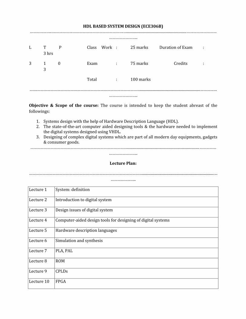
HDL BASED SYSTEM DESIGN (ECE306B) ………………..….…………………………………………………….…..................................................................………………………
……………………..
L T P Class Work : 25 marks Duration of Exam :
3 hrs
3 1 0 Exam : 75 marks Credits :
3
Total : 100 marks
…….…………………………………………………………………………………..................................................................……………
……………………..
Objective & Scope of the course: The course is intended to keep the student abreast of the
followings:
1. Systems design with the help of Hardware Description Language (HDL). 2. The state-of-the-art computer aided designing tools & the hardware needed to implement
the digital systems designed using VHDL. 3. Designing of complex digital systems which are part of all modern day equipments, gadgets
& consumer goods. ……………………………………………………………………………................................................................................……………
……………………..
Lecture Plan:
…………………………………………………………………………………………...............................................................................…
…………………..
Lecture 1 System: definition
Lecture 2 Introduction to digital system
Lecture 3 Design issues of digital system
Lecture 4 Computer-aided design tools for designing of digital systems
Lecture 5 Hardware description languages
Lecture 6 Simulation and synthesis
Lecture 7 PLA, PAL
Lecture 8 ROM
Lecture 9 CPLDs
Lecture 10 FPGA
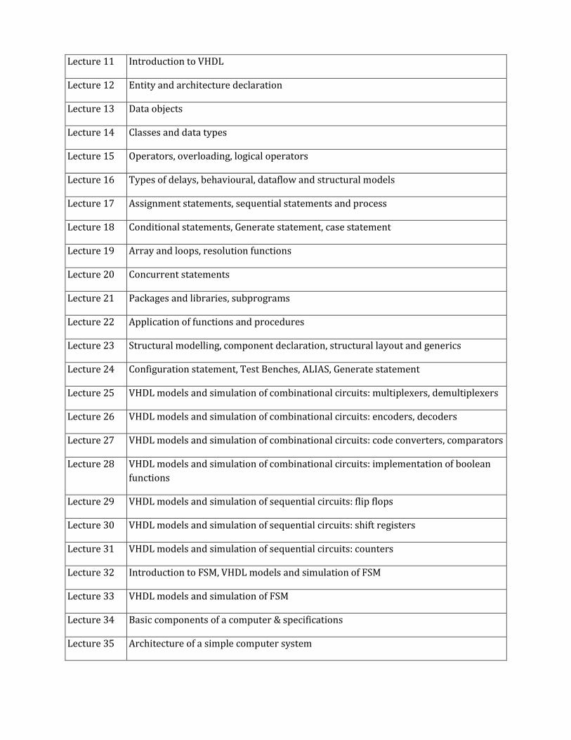
Lecture 11 Introduction to VHDL
Lecture 12 Entity and architecture declaration
Lecture 13 Data objects
Lecture 14 Classes and data types
Lecture 15 Operators, overloading, logical operators
Lecture 16 Types of delays, behavioural, dataflow and structural models
Lecture 17 Assignment statements, sequential statements and process
Lecture 18 Conditional statements, Generate statement, case statement
Lecture 19 Array and loops, resolution functions
Lecture 20 Concurrent statements
Lecture 21 Packages and libraries, subprograms
Lecture 22 Application of functions and procedures
Lecture 23 Structural modelling, component declaration, structural layout and generics
Lecture 24 Configuration statement, Test Benches, ALIAS, Generate statement
Lecture 25 VHDL models and simulation of combinational circuits: multiplexers, demultiplexers
Lecture 26 VHDL models and simulation of combinational circuits: encoders, decoders
Lecture 27 VHDL models and simulation of combinational circuits: code converters, comparators
Lecture 28 VHDL models and simulation of combinational circuits: implementation of boolean
functions
Lecture 29 VHDL models and simulation of sequential circuits: flip flops
Lecture 30 VHDL models and simulation of sequential circuits: shift registers
Lecture 31 VHDL models and simulation of sequential circuits: counters
Lecture 32 Introduction to FSM, VHDL models and simulation of FSM
Lecture 33 VHDL models and simulation of FSM
Lecture 34 Basic components of a computer & specifications
Lecture 35 Architecture of a simple computer system
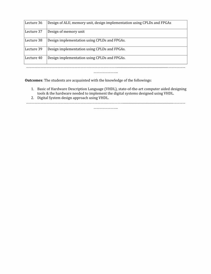
Lecture 36 Design of ALU, memory unit, design implementation using CPLDs and FPGAs
Lecture 37 Design of memory unit
Lecture 38 Design implementation using CPLDs and FPGAs.
Lecture 39 Design implementation using CPLDs and FPGAs.
Lecture 40 Design implementation using CPLDs and FPGAs.
…………………………………………………………………………………….................................................................………………
……………………..
Outcomes: The students are acquainted with the knowledge of the followings:
1. Basic of Hardware Description Language (VHDL), state-of-the-art computer aided designing tools & the hardware needed to implement the digital systems designed using VHDL.
2. Digital System design approach using VHDL. ………………………………………………………………………………………….................................................................…………
……………………..
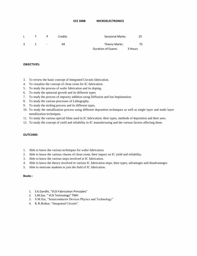
ECE 308B MICROELECTRONICS
L T P Credits Sessional Marks: 25
3 1 - 04 Theory Marks: 75
Duration of Exams: 3 Hours
OBJECTIVES:
3. To review the basic concept of Integrated Circuits fabrication.
4. To visualize the concept of clean room for IC fabrication.
5. To study the process of wafer fabrication and its doping.
6. To study the epitaxial growth and its different types
7. To study the process of impurity addition using Diffusion and Ion Implantation.
8. To study the various processes of Lithography.
9. To study the etching process and its different types.
10. To study the metallization process using different deposition techniques as well as single layer and multi layer
metallization techniques.
11. To study the various special films used in IC fabrication: their types, methods of deposition and their uses.
12. To study the concept of yield and reliability in IC manufacturing and the various factors affecting them.
OUTCOME:
1. Able to know the various techniques for wafer fabrication.
2. Able to know the various classes of clean room, their impact on IC yield and reliability.
3. Able to know the various steps involved in IC fabrication.
4. Able to know the theory involved in various IC fabrication steps, their types, advantages and disadvantages
5. Able to motivate students to join the field of IC fabrication.
Books :
1. S.K.Gandhi, “VLSI Fabrication Principles” 2. S.M.Sze, “ VLSI Technology” TMH 3. S.M.Sze, “Semiconductor Devices Physics and Technology”
4. K.R.Botkar, “Integrated Circuits”.
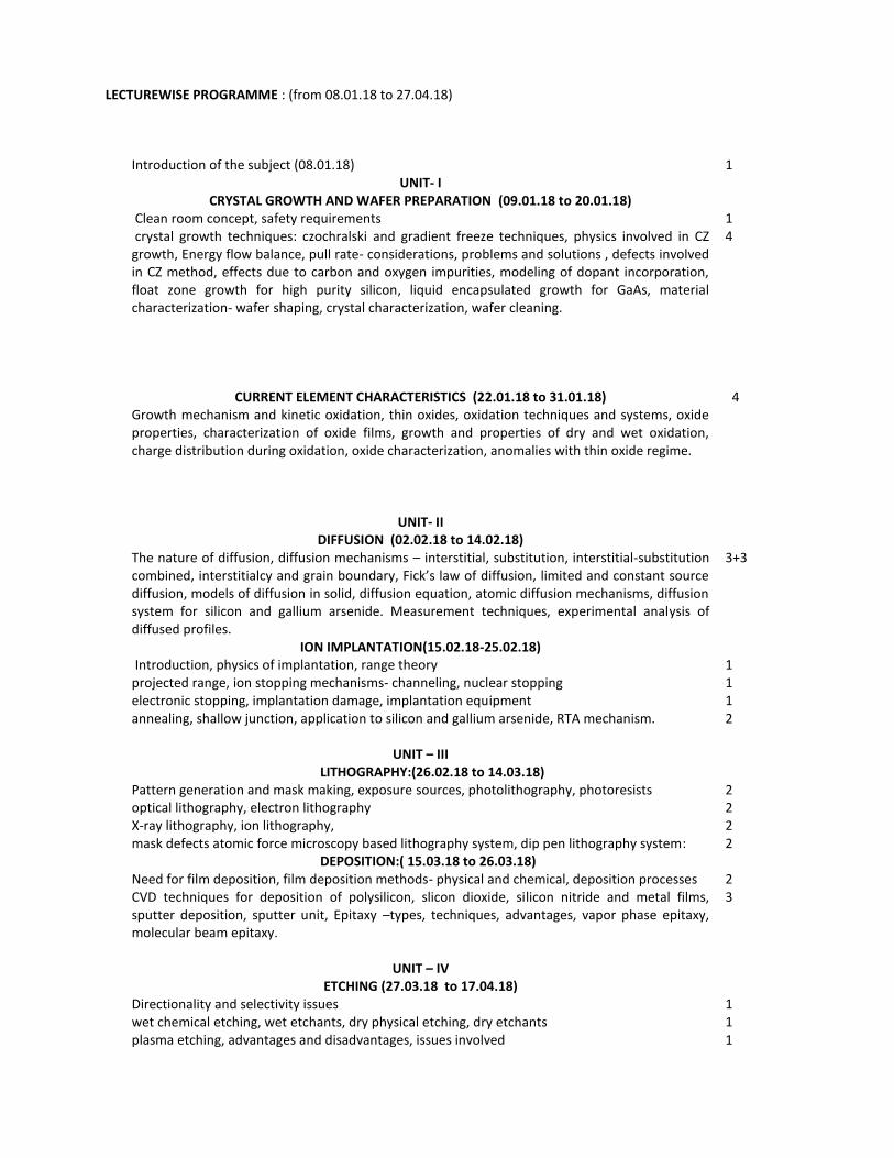
LECTUREWISE PROGRAMME : (from 08.01.18 to 27.04.18)
Introduction of the subject (08.01.18) 1 UNIT- I
CRYSTAL GROWTH AND WAFER PREPARATION (09.01.18 to 20.01.18) Clean room concept, safety requirements 1 crystal growth techniques: czochralski and gradient freeze techniques, physics involved in CZ growth, Energy flow balance, pull rate- considerations, problems and solutions , defects involved in CZ method, effects due to carbon and oxygen impurities, modeling of dopant incorporation, float zone growth for high purity silicon, liquid encapsulated growth for GaAs, material characterization- wafer shaping, crystal characterization, wafer cleaning.
4
CURRENT ELEMENT CHARACTERISTICS (22.01.18 to 31.01.18) Growth mechanism and kinetic oxidation, thin oxides, oxidation techniques and systems, oxide properties, characterization of oxide films, growth and properties of dry and wet oxidation, charge distribution during oxidation, oxide characterization, anomalies with thin oxide regime.
4
UNIT- II DIFFUSION (02.02.18 to 14.02.18)
The nature of diffusion, diffusion mechanisms – interstitial, substitution, interstitial-substitution combined, interstitialcy and grain boundary, Fick’s law of diffusion, limited and constant source diffusion, models of diffusion in solid, diffusion equation, atomic diffusion mechanisms, diffusion system for silicon and gallium arsenide. Measurement techniques, experimental analysis of diffused profiles.
ION IMPLANTATION(15.02.18-25.02.18)
3+3
Introduction, physics of implantation, range theory 1 projected range, ion stopping mechanisms- channeling, nuclear stopping 1 electronic stopping, implantation damage, implantation equipment 1 annealing, shallow junction, application to silicon and gallium arsenide, RTA mechanism.
2
UNIT – III LITHOGRAPHY:(26.02.18 to 14.03.18) Pattern generation and mask making, exposure sources, photolithography, photoresists 2 optical lithography, electron lithography 2 X-ray lithography, ion lithography, 2 mask defects atomic force microscopy based lithography system, dip pen lithography system: 2 DEPOSITION:( 15.03.18 to 26.03.18) Need for film deposition, film deposition methods- physical and chemical, deposition processes 2 CVD techniques for deposition of polysilicon, slicon dioxide, silicon nitride and metal films, sputter deposition, sputter unit, Epitaxy –types, techniques, advantages, vapor phase epitaxy, molecular beam epitaxy.
3
UNIT – IV ETCHING (27.03.18 to 17.04.18)
Directionality and selectivity issues 1 wet chemical etching, wet etchants, dry physical etching, dry etchants 1 plasma etching, advantages and disadvantages, issues involved 1
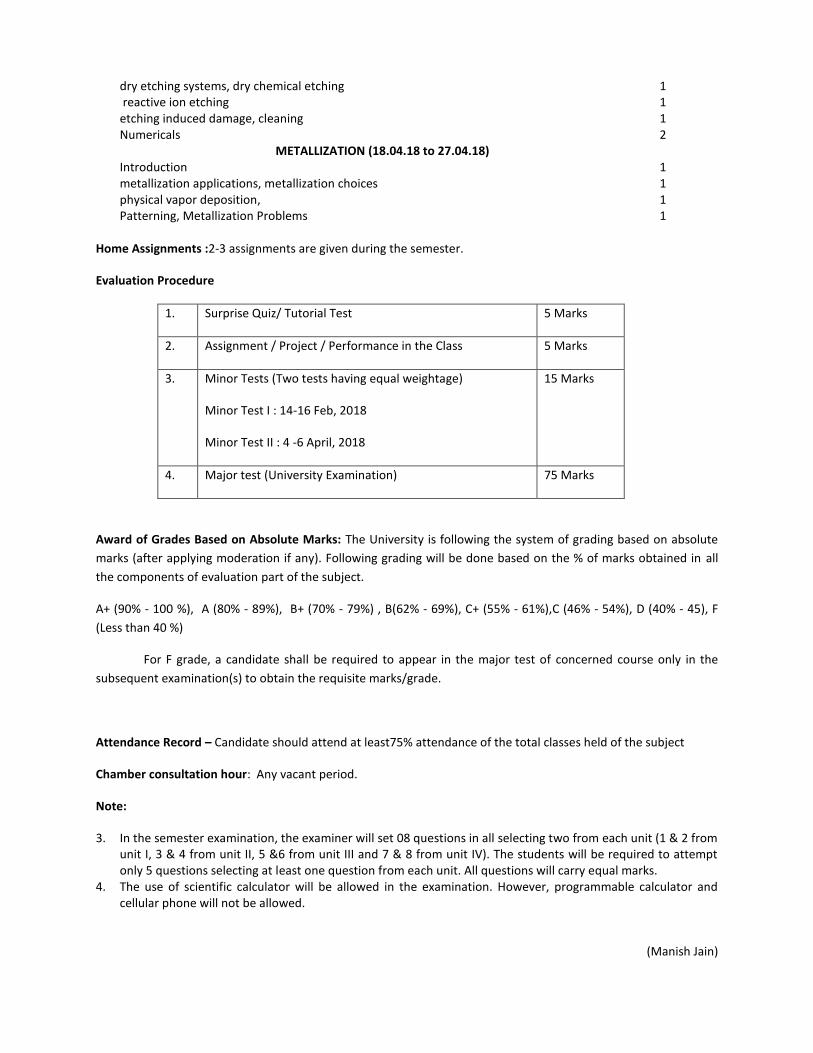
dry etching systems, dry chemical etching 1 reactive ion etching 1 etching induced damage, cleaning 1 Numericals 2
METALLIZATION (18.04.18 to 27.04.18) Introduction 1 metallization applications, metallization choices 1 physical vapor deposition, 1 Patterning, Metallization Problems 1
Home Assignments :2-3 assignments are given during the semester.
Evaluation Procedure
1. Surprise Quiz/ Tutorial Test 5 Marks
2. Assignment / Project / Performance in the Class 5 Marks
3. Minor Tests (Two tests having equal weightage)
Minor Test I : 14-16 Feb, 2018
Minor Test II : 4 -6 April, 2018
15 Marks
4. Major test (University Examination) 75 Marks
Award of Grades Based on Absolute Marks: The University is following the system of grading based on absolute
marks (after applying moderation if any). Following grading will be done based on the % of marks obtained in all
the components of evaluation part of the subject.
A+ (90% - 100 %), A (80% - 89%), B+ (70% - 79%) , B(62% - 69%), C+ (55% - 61%),C (46% - 54%), D (40% - 45), F
(Less than 40 %)
For F grade, a candidate shall be required to appear in the major test of concerned course only in the
subsequent examination(s) to obtain the requisite marks/grade.
Attendance Record – Candidate should attend at least75% attendance of the total classes held of the subject
Chamber consultation hour: Any vacant period.
Note:
3. In the semester examination, the examiner will set 08 questions in all selecting two from each unit (1 & 2 from unit I, 3 & 4 from unit II, 5 &6 from unit III and 7 & 8 from unit IV). The students will be required to attempt only 5 questions selecting at least one question from each unit. All questions will carry equal marks.
4. The use of scientific calculator will be allowed in the examination. However, programmable calculator and cellular phone will not be allowed.
(Manish Jain)
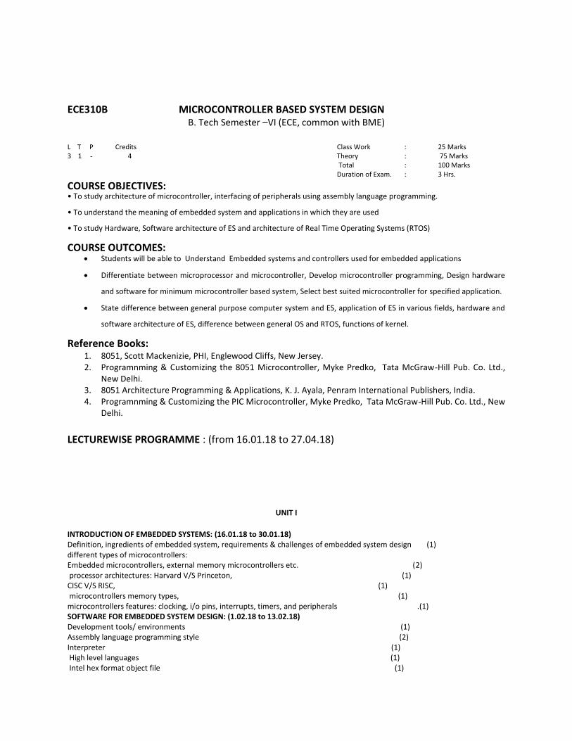
ECE310B MICROCONTROLLER BASED SYSTEM DESIGN B. Tech Semester –VI (ECE, common with BME)
L T P Credits Class Work : 25 Marks 3 1 - 4 Theory : 75 Marks
Total : 100 Marks Duration of Exam. : 3 Hrs.
COURSE OBJECTIVES:
• To study architecture of microcontroller, interfacing of peripherals using assembly language programming.
• To understand the meaning of embedded system and applications in which they are used
• To study Hardware, Software architecture of ES and architecture of Real Time Operating Systems (RTOS)
COURSE OUTCOMES: Students will be able to Understand Embedded systems and controllers used for embedded applications
Differentiate between microprocessor and microcontroller, Develop microcontroller programming, Design hardware
and software for minimum microcontroller based system, Select best suited microcontroller for specified application.
State difference between general purpose computer system and ES, application of ES in various fields, hardware and
software architecture of ES, difference between general OS and RTOS, functions of kernel.
Reference Books: 1. 8051, Scott Mackenizie, PHI, Englewood Cliffs, New Jersey. 2. Programnming & Customizing the 8051 Microcontroller, Myke Predko, Tata McGraw-Hill Pub. Co. Ltd.,
New Delhi. 3. 8051 Architecture Programming & Applications, K. J. Ayala, Penram International Publishers, India. 4. Programnming & Customizing the PIC Microcontroller, Myke Predko, Tata McGraw-Hill Pub. Co. Ltd., New
Delhi.
LECTUREWISE PROGRAMME : (from 16.01.18 to 27.04.18)
UNIT I
INTRODUCTION OF EMBEDDED SYSTEMS: (16.01.18 to 30.01.18) Definition, ingredients of embedded system, requirements & challenges of embedded system design (1) different types of microcontrollers: Embedded microcontrollers, external memory microcontrollers etc. (2) processor architectures: Harvard V/S Princeton, (1) CISC V/S RISC, (1) microcontrollers memory types, (1) microcontrollers features: clocking, i/o pins, interrupts, timers, and peripherals .(1) SOFTWARE FOR EMBEDDED SYSTEM DESIGN: (1.02.18 to 13.02.18) Development tools/ environments (1) Assembly language programming style (2) Interpreter (1) High level languages (1) Intel hex format object file (1)
Debugging (1)
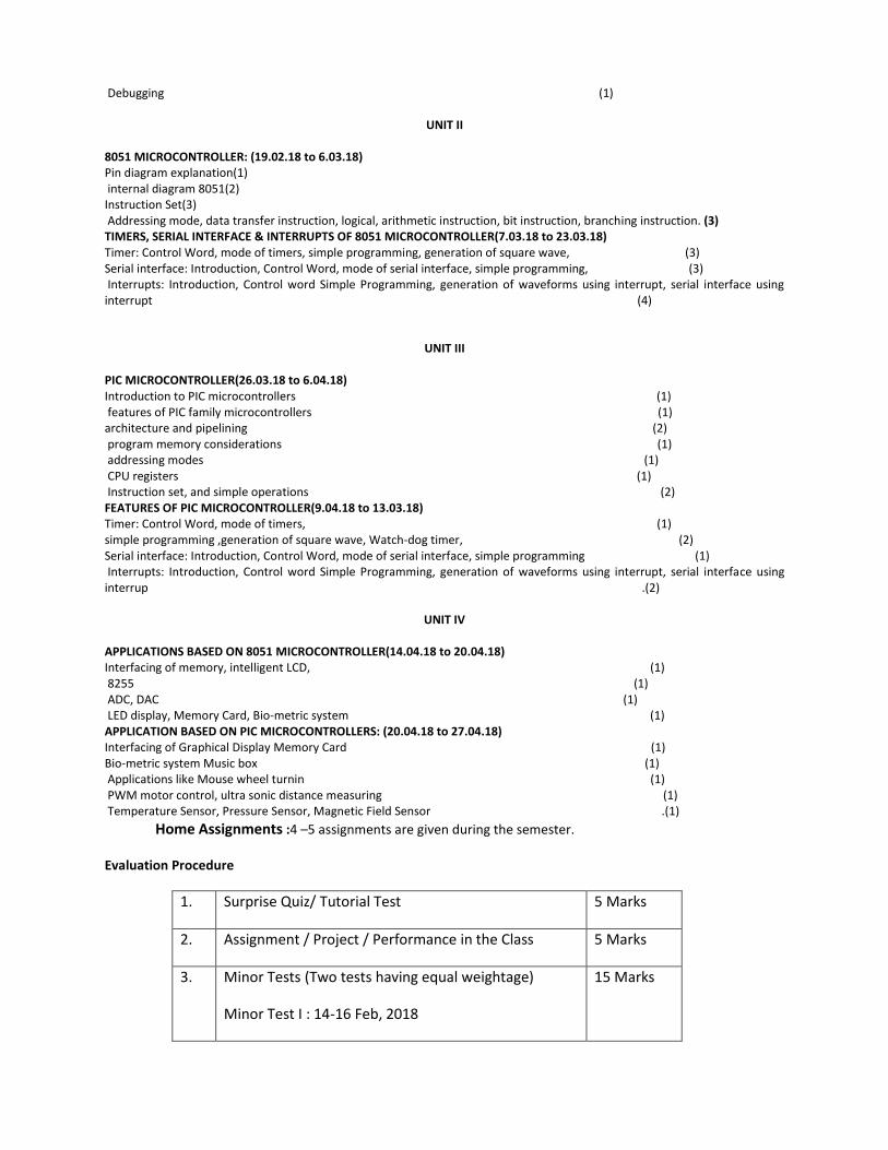
UNIT II 8051 MICROCONTROLLER: (19.02.18 to 6.03.18) Pin diagram explanation(1) internal diagram 8051(2) Instruction Set(3) Addressing mode, data transfer instruction, logical, arithmetic instruction, bit instruction, branching instruction. (3) TIMERS, SERIAL INTERFACE & INTERRUPTS OF 8051 MICROCONTROLLER(7.03.18 to 23.03.18) Timer: Control Word, mode of timers, simple programming, generation of square wave, (3) Serial interface: Introduction, Control Word, mode of serial interface, simple programming, (3) Interrupts: Introduction, Control word Simple Programming, generation of waveforms using interrupt, serial interface using interrupt (4)
UNIT III PIC MICROCONTROLLER(26.03.18 to 6.04.18) Introduction to PIC microcontrollers (1) features of PIC family microcontrollers (1) architecture and pipelining (2) program memory considerations (1) addressing modes (1) CPU registers (1) Instruction set, and simple operations (2) FEATURES OF PIC MICROCONTROLLER(9.04.18 to 13.03.18) Timer: Control Word, mode of timers, (1) simple programming ,generation of square wave, Watch-dog timer, (2) Serial interface: Introduction, Control Word, mode of serial interface, simple programming (1) Interrupts: Introduction, Control word Simple Programming, generation of waveforms using interrupt, serial interface using interrup .(2)
UNIT IV APPLICATIONS BASED ON 8051 MICROCONTROLLER(14.04.18 to 20.04.18) Interfacing of memory, intelligent LCD, (1) 8255 (1) ADC, DAC (1) LED display, Memory Card, Bio-metric system (1) APPLICATION BASED ON PIC MICROCONTROLLERS: (20.04.18 to 27.04.18) Interfacing of Graphical Display Memory Card (1) Bio-metric system Music box (1) Applications like Mouse wheel turnin (1) PWM motor control, ultra sonic distance measuring (1) Temperature Sensor, Pressure Sensor, Magnetic Field Sensor .(1)
Home Assignments :4 –5 assignments are given during the semester.
Evaluation Procedure
1. Surprise Quiz/ Tutorial Test 5 Marks
2. Assignment / Project / Performance in the Class 5 Marks
3. Minor Tests (Two tests having equal weightage)
Minor Test I : 14-16 Feb, 2018
15 Marks
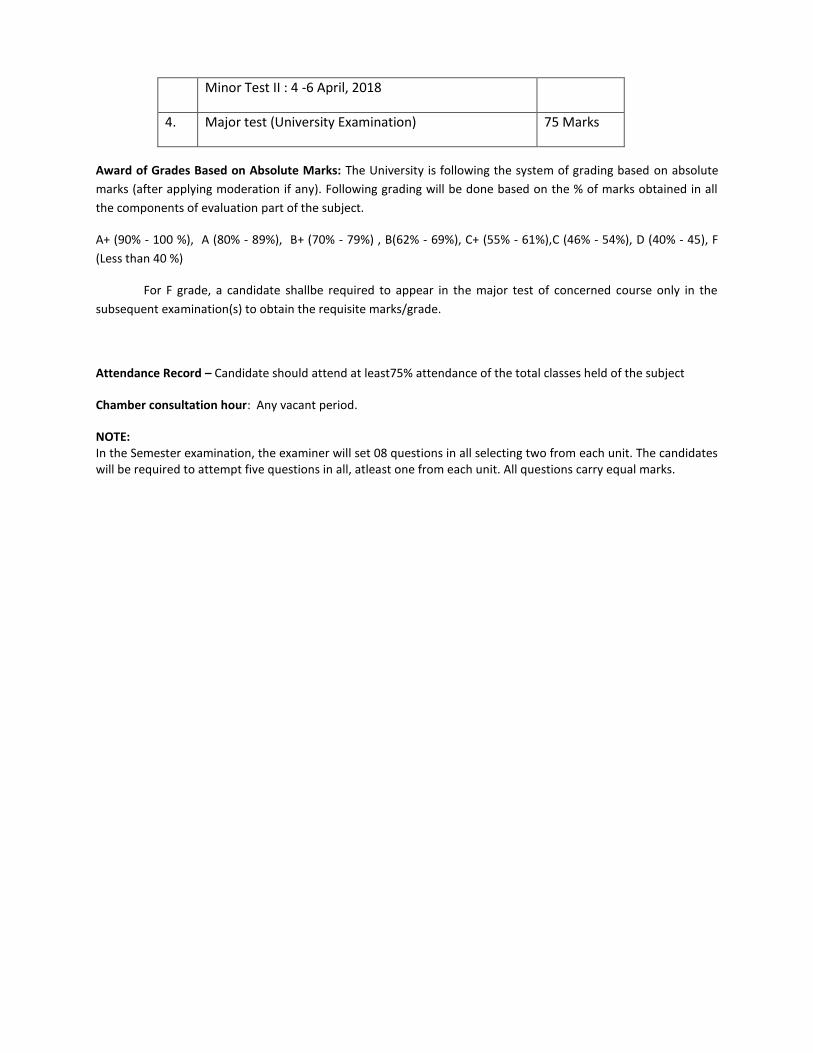
Minor Test II : 4 -6 April, 2018
4. Major test (University Examination) 75 Marks
Award of Grades Based on Absolute Marks: The University is following the system of grading based on absolute
marks (after applying moderation if any). Following grading will be done based on the % of marks obtained in all
the components of evaluation part of the subject.
A+ (90% - 100 %), A (80% - 89%), B+ (70% - 79%) , B(62% - 69%), C+ (55% - 61%),C (46% - 54%), D (40% - 45), F
(Less than 40 %)
For F grade, a candidate shallbe required to appear in the major test of concerned course only in the
subsequent examination(s) to obtain the requisite marks/grade.
Attendance Record – Candidate should attend at least75% attendance of the total classes held of the subject
Chamber consultation hour: Any vacant period.
NOTE: In the Semester examination, the examiner will set 08 questions in all selecting two from each unit. The candidates will be required to attempt five questions in all, atleast one from each unit. All questions carry equal marks.
ECE322B MICROWAVE AND RADAR ENGINEERING LAB
L T P Credits Class Work : 20 Marks - - 2 1 Theory : 30 Marks
Total : 50 Marks
Duration of Exam. : 3 Hrs.
OBJECTIVES:
13. The goal of this course is to introduce students the various microwave components.
14. To provide understanding about the operation of different types of Microwave devices.
15. To provide various methods of measurement for measuring variable parameters of microwave devices.
OUTCOME:
6. The students will have complete knowledge about all the microwave devices and their operational mechanism.
7. The students will become proficient in measuring various parameters related to microwave devices.
8. The students will be able to plot various voltage and power characteristic curves required for better understanding of the device.
Books :
1. Foundations for Microwave Engineering: R.E.Collin, MGH 2. Microwave Devices and Circuit: Samuel Liao, PHI. 3. Elements of Microwave Engineering : R.Chatterjee, EWP
LAB PROGRAMME : (from 15.01.18 to 27.04.18)
Introduction of the Lab (15.01.18) 1
Experiments
1. To study the Wave guide Components.
2. Generation of Microwave Power & Basic set-up.
3. To Study the characteristic of reflex klystron.
4. To measure frequency of Microwave source and demonstrate relationship among frequency, free space
wavelength and guide wave length.
1 1 1 1
5. To measure VSWR of an unknown load.
6. To measure large standing wave ratio of a unmatched load.
7. To measure VSWR, insertion loss and attenuation of a fixed and variable attenuator.
8. To measure coupling factor and directivity of Directional coupler.
9. To determine the insertion loss, isolation of three port circulator
10. To determine the insertion loss, isolation of a isolator.
11. To study the characteristics of Gunn Diode.
1 1 1 1 1 1
1
Home Assignments : 3-4 assignments regarding lab experiments are given during the semester.
Evaluation Procedure
1. Surprise Quiz 5 Marks
2. Assignment / Performance in the Class 5 Marks
3. File 5 Marks
4 Internal Viva 5Marks
5 Theory Test 30 Marks
Award of Grades Based on Absolute Marks: The University is following the system of grading based on absolute marks (after applying
moderation if any). Following grading will be done based on the % of marks obtained in all the components of evaluation part of the subject.
A+ (90% - 100 %), A(80% - 89%), B+ (70% - 79%) , B(62% - 69%), C+ (55% - 61%),C (46% - 54%), D (40% - 45), F (Less than 40 %)
For F grade, a candidate shallbe required to appear in the major test of concerned course only in the subsequent examination(s) to
obtain the requisite marks/grade.
Attendance Record – Candidate should attend at least75% attendance of the total classes held of the subject
Chamber consultation hour: Any vacant period.
NOTE:
7 experiments are to be performed from the above list. Remaining 3 can be performed depending upon the
infrastructure available and ECE322B contents.
(kusum dalal)
ECE326B HDL BASED SYSTEM DESIGN LAB B. Tech Semester –VI (ECE, AEI)
L T P Credits Class Work : 20 Marks - - 2 1 Practical : 30 Marks
Total : 50 Marks
COURSE OBJECTIVES:
1. Design of basic combinational and sequential digital systems through HDL
COURSE OUTCOMES:
2. VHDL coding flow
3. ASIC Design Flow
Reference Books: 1. “IEEE Standard VHDL Language Reference Manual (1993)”. 2. “Digital design”, Ashenden, Elsevier. 3. “Digital Design and Modelling with VHDL and Synthesis”, K. C. Chang; IEEE Computer Society Press. 4. "A VHDL Primmer”, J. Bhasker, Prentice Hall 1995. 5. “Digital System Design using VHDL”, Charles. H. Roth, PWS (1998). 6. "VHDL-Analysis & Modelling of Digital Systems”, Z. Navabi, McGraw Hill. 7. “VHDL”, Perry, TMH (2002). 8. “Introduction to Digital Systems”, Ercegovac. Lang & Moreno, John Wiley (1999). 9. “Fundamentals of Digital Logic with VHDL”, Brown and Vranesic; TMH (2000) 10. “Modern Digital Electronics”, R. P. Jain, TMH (2003). 11. “Digital system Design using FPGA & CPLD'S”, Grout, Elsevier. 12. “VHDL”, Kaur, Pearson. 13. “Circuit Design & Simulation with VHDL”, Volnei A. Pedroni, PHI.
LIST OF EXPERIMENTS:
1. Design all Basic gates using HDL.(15.1.18)
2. Design Universal gates using HDL.(29.1.18)
3. Write VHDL programs for half adder and full adder circuits, check the wave forms and the hardware
generated.(5.2.18)
4. Write VHDL programs for multiplexer & demultiplexer circuits, check the wave forms and the hardware
generated.(12.2.18)
5. Write VHDL programs for the following circuits, check the wave forms and the hardware generated
a. decoder
b. encode(26.2.18)
6. Write a VHDL program for a comparator and check the wave forms and the hardware generated. (5.3.18)
7. Write a VHDL program for a code converter and check the wave forms and the hardware generated.(12.3.18)
8. Write a VHDL program for a FLIP-FLOP and check the wave forms and the hardware generated. (19.3.18)
9. Write a VHDL program for a counter and check the wave forms and the hardware generated. (26.3.18)
10. Write VHDL programs for the following circuits, check the wave forms and the hardware generated
(a) Register(2.4.18)
(b) Shift register(9.4.18)
11. Implement any three (given above) on FPGA kit.(16.4.18)
12. Implement any three (given above) on CPLD kit.(23.4.18)
Note:- 1 Total ten experiments are to be performed in the semester. 2 At least seven experiments should be performed from the above list. Remaining three experiments should be
performed as designed and set by the concerned institution as per the scope of the syllabus
ECE330B MICROCONTROLLER LAB B. Tech Semester –VI (ECE, common with BME)
L T P Credits Class Work : 20 Marks - - 2 1 Practical : 30 Marks
Total : 50 Marks Duration of Exam. : 3 Hrs.
COURSE OBJECTIVES: Understand need of microprocessors, microcontrollers in development of various projects and to know complete
architectural, programming, interfacing details of 8051 microcontroller
COURSE OUTCOMES:
Design of few logics using modules of controller
Reference Books: 5. 8051, Scott Mackenizie, PHI, Englewood Cliffs, New Jersey. 6. Programnming & Customizing the 8051 Microcontroller, Myke Predko, Tata McGraw-Hill Pub. Co. Ltd., New Delhi. 7. 8051 Architecture Programming & Applications, K. J. Ayala, Penram International Publishers, India. 8. Programnming & Customizing the PIC Microcontroller, Myke Predko, Tata McGraw-Hill Pub. Co. Ltd., New Delhi.
LIST OF EXPERIMENTS
1. Study Architecture of 8051 Microcontroller & Power on reset circuit
.(17.1.18)
2. (a) Write an assembly language program to add eight 8-bit numbers.
(24.1.18)
(b) Write an assembly language program to find average of eight 8-bit numbers.
(7.2.18)
3. (a) Write an assembly language program to find a maximum number from a given 8-bit ten numbers. (
21.2.18)
(b) Write an assembly language program to find a minimum number from a given 8-bit ten numbers.
(28.2.18)
4. Arrange the given ten 8-bit numbers in ascending order.
(7.3.18)
5. Generate a square wave of 10kHz at P1.0 Crystal frequency is XXXX .(
14.3.18)
6. Write a program to transfer data from given memory block B1 to block B2.
(21.3.18)
7. Interface LED and switch with microcontroller 8051 or PIC. (
28.3.18)
8. Interface seven segment display with microcontroller 8051 or PIC.
(4.4.18)
9. Interface LCD with microcontroller 8051 or PIC. (
11.4.18)
10. Write an assembly language program for External program and test on hardware.
(18.4.18)
11. Interface stepper motor with microcontroller 8051 or PIC.
(25.4..18)
Note:-
1 Total ten experiments are to be performed in the semester. 2 At least seven experiments should be performed from the above list. Remaining three experiments should be
performed as designed and set by the concerned institution as per the scope of the syllabus.
ECE 312B COMMUNICATION SYSTEM AND TECHNOLOGY
L T P Credits Class Work : 25 Marks
3 1 - 4 Theory : 75 Marks
Total : 100 Marks
Duration of Exam. : 3 Hrs.
Course Objective:
OBJECTIVES:
9. This course provides a thorough introduction to the basic principles and techniques used in analog and digital
communications.
10. The course will introduce analog and digital modulation techniques, communication receiver and transmitter
design, baseband and bandpass communication techniques, line coding techniques, noise analysis and
multiplexing techniques.
11. The course also introduces analytical techniques to evaluate the performance of communication systems.
OUTCOME:
1. On successful completion of the course students will be able to understand basic elements of a
communication system.
2. Conduct analysis of baseband signals in time domain and in frequency domain and Demonstrate
understanding of various analog and digital modulation and demodulation techniques.
3. Analyse the performance of modulation and demodulation techniques in various transmission
environments and appreciate the importance of synchronisation in communication systems.
Books:
1. Communication Systems, By Manoj Duhan – I. K. International.
2. Electronic Communication Systems, By Kennedy – TMH.
3. Communication Systems, By Singh & Sapre – TMH.
4. Electronic Communication, By Roody Coolen – Pearson.
5. Analog Communication, By P. Chakarbarti – DR & Co.
6. Communication Systems, By Simon Haykins – Wiley Seeger.
LECTUREWISE PROGRAMME: (from 08.01.18 to 27.04.18)
Introduction of the subject (08.01.18) 1 UNIT- I
INTRODUCTION TO COMMUNICATION SYSTEM (09.01.18 to 20.01.18) Introduction: Modulation, Demodulation 1 Radio Frequency Spectrum, Signals & their classification 1 Limitations & Advantages of a Communication System, Comparison of Analog & Digital Communication Systems 1 Historical Perspective, Modes & Medias of Communication.
2
NOISE (23.01.18 to 31.01.18) Sources of Noise, External & Internal Noise, Noise Calculations, Noise Figure, Noise Figure Calculation, Noise Temperature, Noise in Communication Systems, Band Pass Noise Model
3
Cascaded States & its Noise Figure Calculation, Signal in presence of Noise, Pre-Emphasis & De- Emphasis, Noise Quieting Effect, Capture Effect and Noise in Modulation Systems.
2
UNIT- II LINEAR MODULATION and ANGLE MODULATION (02.02.18 to 23.02.18)
Amplitude Modulation: Basic definition & derivation for Modulation & Modulation Index, Modulation & Demodulation of AM, Suppressed Carrier Modulation, Quadrature Amplitude Modulation
2
SSB-SC, DSB-SC, VSB Modulation & Demodulation, Comparison of various AM Systems, Generation of AM waves. 3 Angle Modulation: Basic definition & derivation for Modulation & Modulation Index, Generation of FM waves, Comparison between PM & FM, Frequency Spectrum of FM, B.W. & required spectra, Types of FM, vector representation of FM
3
Universal Curve, Multiple FM, Demodulation of FM waves, Demodulation of PM waves, Comparison between AM & FM.
2
UNIT – III PULSE ANALOG MODULATION (26.02.18 to 14.03.18)
Sampling theory 1 Time Division Multiplexing, Frequency Division Multiplexing 1 Pulse Amplitude Modulation, Pulse Width Modulation, Pulse Position Modulation 3
PULSE DIGITAL MODULATION ( 16.03.18 to 26.03.18) Elements of Pulse Code Modulation, Noise in PCM Systems, Bandwidth of PCM Systems, Measure of Information, Channel Capacity, Channel Capacity of PCM System
2
Differential Pulse Code Modulation (DPCM), Delta Modulation (DM), Digital Modulation: ASK, FSK, PSK, DPSK.
3
UNIT – IV OPTICALCOMMUNICATION SYSTEMS (27.03.18 to 17.04.18)
Types of Optical Fibres: Step Index & Graded Index, Multi mode & Single mode 2 Attenuation & Dispersion in fibres, Optical transmitters LEDS & Laser Diode 2 Optical Receivers-PIN & APDS, optical fiber link. 2
MICROWAVE COMMUNICATIONS (18.04.18 to 27.04.18) Transmit & receive antennas, link budget, line of sight systems, Satellite-link-GT ratio of earth stations 2 VSATS & GPSS.
2
Home Assignments: 4 –5 assignments are given during the semester.
Evaluation Procedure
1. Surprise Quiz/ Tutorial Test 5 Marks
2. Assignment / Project / Performance in the Class 5 Marks
3. Minor Tests (Two tests having equal weightage)
Minor Test I : 14-16 Feb, 2018
Minor Test II : 4 -6 April, 2018
15 Marks
4. Major test (University Examination) 75 Marks
Award of Grades Based on Absolute Marks: The University is following the system of grading based on absolute marks (after applying
moderation if any). Following grading will be done based on the % of marks obtained in all the components of evaluation part of the subject.
A+ (90% - 100 %), A (80% - 89%), B+ (70% - 79%) , B(62% - 69%), C+ (55% - 61%),C (46% - 54%), D (40% - 45), F (Less than 40 %)
For F grade, a candidate shallbe required to appear in the major test of concerned course only in the subsequent examination(s) to
obtain the requisite marks/grade.
Attendance Record – Candidate should attend at least 75% attendance of the total classes held of the subject
Chamber consultation hour: Any vacant period.
Note:
In the semester examination, the examiner will select two questions from each unit (total eight questions in
all), covering the entire syllabus. The student will be required to attempt five questions, selecting at least one
question from each unit.
(Dr. Poonam Singal)
ECE402B WIRELESS COMMUNICATION SYSTEMS (VIII)
L T P Credits Sessional Marks: 25
4 - - 04 Theory Marks: 75
Duration of Exams: 3 Hours
OBJECTIVES:
16. To Review the Basic Concept of Mobile Radio Communication.
17. To Develop an Intuitive Understanding of Various Generations of Wireless Communication.
18. To Study the Cellular System Design Fundamentals and to Understand the Concept of Capacity Enhancement of Cellular Systems.
19. To Analyze the Mobile Radio Propagation Models and to Understand the Concept of Indoor and Outdoor Propagation Models.
20. To Study Effect of Interference on Microwaves and Methods Used to Avoid/Remove Interference Effect on Wireless Communication.
21. To Get the Idea of Multiplexing and Multiple Access Techniques for Enhancement of Capacity of Cellular Systems.
22. To Develop an Intuitive Understanding of Wireless Networking and to Study Various Protocols Used for Wireless Networking.
23. To Study Various Wireless Systems and Standards i.e. GSM, CDMA etc.
OUTCOME:
12. Able to Know the Basic Concept of Mobile Radio Communication.
13. Able to Know Various Generations of Wireless Communication and Difference Between 1G, 2G, 3G and 4G.
14. Able to Know Cellular System Design Fundamentals i.eFrequency Reuse, Channel Assignment Strategies, Hand-Off Strategies, Interference
and System Capacity, Trunking and Grade of Service etc.
15. Able to Know the Mobile Radio Propagation Models and Basic Concept of Radio Wave Propagation i.eFree Space Propagation Model,
Practical Link Budget Design Using Path Loss Models, Outdoor Propagation Models, Indoor Propagation Models, Signal Penetration Into
Buildings.
16. Able to Know the Effect of Interference on Microwaves.
17. Able to Know the Multiplexing and Multiple Access Techniques for Enhancement of the Capacity of Cellular Systems i.eFrequency Division
Multiple Access (FDMA), Time Division Multiple Access (TDMA), Spread Spectrum Multiple Access, Space Division Multiple Access (SDMA),
etc.
18. Able to Know the Concept of Wireless Networking and Various Protocols i.e ISDN, SS7 etc.
19. Able to Know Various Wireless Systems and Standards i.e GSM, CDMA etc.
20. Able to Imbue the Motivation in Students for Continuous Learning and Improvement of Technical Advancement & Skills in the Field of
Wireless Communication.
Text Books :
1. T.S. Rappaport, “Wireless Communication, Principles & Practice,” PHI . 2. RajeshwarDass, “Wireless Communication Systems,” I.K International Pvt. Ltd 3. JochenSchiller, “Mobile Communication,” Pearson Education
Reference Books:
1. William, C Y Lee, “Mobile Cellular Telecommunications,” Mc Graw Hill 2. Dr. KamiloFeher“Wireless and Digital Communication,” PHI
ECE 404B DATA COMMUNICATION AND NETWORK
L T P Credits Sessional Marks: 25
3 1 - 04 Theory Marks: 75
Duration of Exams: 3 Hours
OBJECTIVES:
1. To review the basic concepts of Data and its various types.
2. To study the various means of data transmission and their comparison. .
3. To study the concept of computer networking, their different types giving advantages and disadvantages of
each with their applications.
4. To study the various types of multiplexing with their applications.
5. To study the network models
6. To study the switching technology used in data communication..
7. To study the data link protocols.
8. To study the wired Lans- Ethernet.
OUTCOME:
1 . Able to know the concept of data, its significance and its types..
2. Able to know the various computer networking models, their advantages and disadvantages..
3. Able to know the various types of multiplexing used in data communication.
4. Able to know the basic concept of reference models and their significance
5. Able to motivate students to join the field of computer networking
Books :
1. Data Communication and Networking by Behrouz.A.Forouzan(TMH Publication)
2. Computer Networks by William Stallings
LECTUREWISE PROGRAMME : (from 08.01.18 to 27.04.18)
Introduction of the subject (08.01.18) 1 UNIT- I
Data Communication and Networks (09.01.18 to 20.01.18) Components, Data Representation 1 Data Flow, Guided and Unguided Media, Distributed Processing 1 Network Criteria, Physical Structure, 1
Network Models, Category of Networks
2
Data and Signals (22.01.18 to 31.01.18) Analog and Digital Data,Analog and Digital Signals,Periodic and Non Periodic Signals,Transmission Impairments-Attenuation,Distortion,Noise,Performance bandwidth,Throughput,Latency,Bandwidth-Delay Product,Jitter
3
Numericals 1 UNIT- II
Digital Transmission:(01.02.18 to 14.02.18) Digital to digital Conversion-Line Coding,Line Coding Schemes,Block Coding,Scrambling 3 Transmission modes-Parallel Transmission 1 Serial Transmission 1 Numericals 1
Multiplexing (15.02.18 to 25.02.18) Frequency Division Multiplexing Wave Division Multiplexing Synchronous Time Division Multiplexing Statistical Time Division Multiplexing
UNIT – III
1 1 1 1
Switching (26.02.18 to 14.03.18) Circuit Switched Networks-Three Phases,Efficiency Delay,Datagram 2 Networks-Routing table, Efficiency, delay 2 Virtual Circuit Networks-Addressing ,Three Phases,Efficiency,Delay in Virtual Circuit Networks 2 Numericals 2
Data Link Control( 15.03.18 to 26.03.18) Framing-Fixed Size Framing,Variable Sized framing,Flow and Error Control-Flow Control,error control,Protocols;
2
Noiseless Channels-Simplest protocol,stop and Wait Protocol,Noisy Channels-Stop and Wait Automatic Repeat Request,Go Back n Automatic Repeat request,Selective Repeat Automatic Repeat request,PiggyBacking
3
UNIT – IV Network Models (27.03.18 to 17.04.18)
Layered Tasks-Sender,receiver and Carier 1 The OSI Model-Layered Architecture,Peer to peer processes,Encapsulation,Layers in the OSI Model
1
Physical Layer 1 data Link layer,Network layer 1 transport layer,Session layer 1 Presentation layer,application layer 1 Summary of layers,Introduction to TCP-IP and Internetworking
2
Wired Lans-Ethernet (18.04.18 to 27.04.18) IEEE Standards-Data Link Layer,Physical layer,Standard 1 Ethernet-Mac Sublayer,Physical layer,Changes in the standard bridged Ethernet 1 Switched Ethernet,full duplex, 1 Ethernet,fast Ethernet-Mac sublayer,Physical layer 1
Home Assignments :3-4 assignments are given during the semester.
Evaluation Procedure
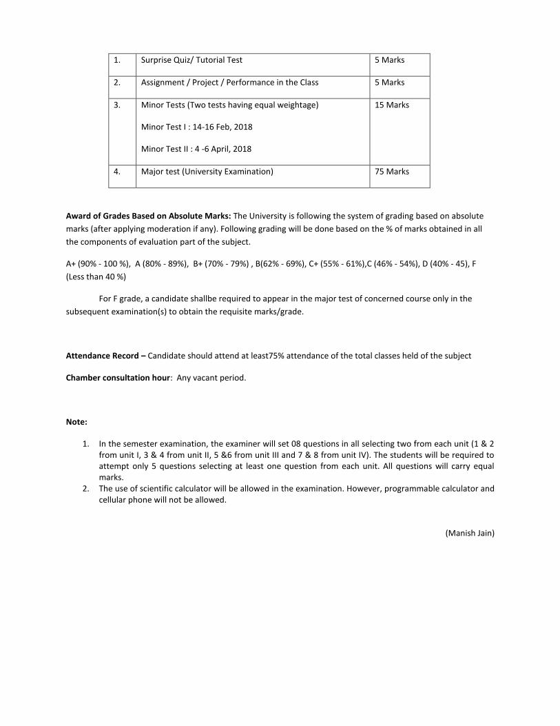
1. Surprise Quiz/ Tutorial Test 5 Marks
2. Assignment / Project / Performance in the Class 5 Marks
3. Minor Tests (Two tests having equal weightage)
Minor Test I : 14-16 Feb, 2018
Minor Test II : 4 -6 April, 2018
15 Marks
4. Major test (University Examination) 75 Marks
Award of Grades Based on Absolute Marks: The University is following the system of grading based on absolute
marks (after applying moderation if any). Following grading will be done based on the % of marks obtained in all
the components of evaluation part of the subject.
A+ (90% - 100 %), A (80% - 89%), B+ (70% - 79%) , B(62% - 69%), C+ (55% - 61%),C (46% - 54%), D (40% - 45), F
(Less than 40 %)
For F grade, a candidate shallbe required to appear in the major test of concerned course only in the
subsequent examination(s) to obtain the requisite marks/grade.
Attendance Record – Candidate should attend at least75% attendance of the total classes held of the subject
Chamber consultation hour: Any vacant period.
Note:
1. In the semester examination, the examiner will set 08 questions in all selecting two from each unit (1 & 2 from unit I, 3 & 4 from unit II, 5 &6 from unit III and 7 & 8 from unit IV). The students will be required to attempt only 5 questions selecting at least one question from each unit. All questions will carry equal marks.
2. The use of scientific calculator will be allowed in the examination. However, programmable calculator and cellular phone will not be allowed.
(Manish Jain)
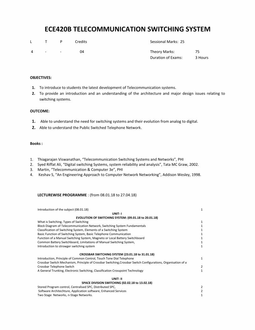
ECE420B TELECOMMUNICATION SWITCHING SYSTEM
L T P Credits Sessional Marks: 25
4 - - 04 Theory Marks: 75
Duration of Exams: 3 Hours
OBJECTIVES:
1. To introduce to students the latest development of Telecommunication systems.
2. To provide an introduction and an understanding of the architecture and major design issues relating to
switching systems.
OUTCOME:
1. Able to understand the need for switching systems and their evolution from analog to digital.
2. Able to understand the Public Switched Telephone Network.
Books :
1. Thiagarajan Viswanathan, “Telecommunication Switching Systems and Networks”, PHI 2. Syed Riffat Ali, “Digital switching Systems, system reliability and analysis”, Tata MC Graw, 2002. 3. Martin, “Telecommunication & Computer 3e”, PHI 4. Keshav S, “An Engineering Approach to Computer Network Networking”, Addison Wesley, 1998.
LECTUREWISE PROGRAMME : (from 08.01.18 to 27.04.18)
Introduction of the subject (08.01.18) 1 UNIT- I
EVOLUTION OF SWITCHING SYSTEM: (09.01.18 to 20.01.18) What is Switching, Types of Switching 1 Block Diagram of Telecommunication Network, Switching System Fundamentals 1 Classification of Switching System, Elements of a Switching System 1 Basic Function of Switching System, Basic Telephone Communication Function of a Manual Switching System, Magneto or Local Battery Switchboard Common Battery Switchboard, Limitations of Manual Switching System, Introduction to strowger switching system
1 1 1 1
CROSSBAR SWITCHING SYSTEM (23.01.18 to 31.01.18) Introduction, Principle of Common Control, Touch Tone Dial Telephone 1 Crossbar Switch Mechanism, Principle of Crossbar Switching,Crossbar Switch Configurations, Organisation of a Crossbar Telephone Switch A General Trunking, Electronic Switching, Classification Crosspoint Technology
2 1
UNIT- II SPACE DIVISION SWITCHING (02.02.18 to 13.02.18)
Stored Program control, Centralised SPC, Distributed SPC, Software Architechture, Application software, Enhanced Services Two Stage Networks, n-Stage Networks.
2 2 1
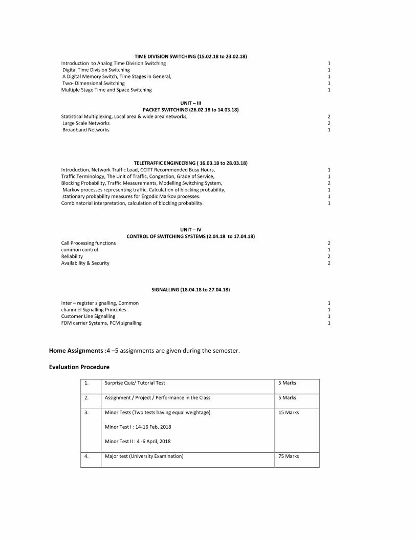
TIME DIVISION SWITCHING (15.02.18 to 23.02.18) Introduction to Analog Time Division Switching Digital Time Division Switching A Digital Memory Switch, Time Stages in General, Two- Dimensional Switching
1 1 1 1
Multiple Stage Time and Space Switching 1
UNIT – III
PACKET SWITCHING (26.02.18 to 14.03.18) Statistical Multiplexing, Local area & wide area networks, Large Scale Networks Broadband Networks
2 2 1
TELETRAFFIC ENGINEERING ( 16.03.18 to 28.03.18) Introduction, Network Traffic Load, CCITT Recommended Busy Hours, Traffic Terminology, The Unit of Traffic, Congestion, Grade of Service, Blocking Probability, Traffic Measurements, Modelling Switching System, Markov processes representing traffic, Calculation of blocking probability, stationary probability measures for Ergodic Markov processes. Combinatorial interpretation, calculation of blocking probability.
1 1 2 1 1 1
UNIT – IV CONTROL OF SWITCHING SYSTEMS (2.04.18 to 17.04.18)
Call Processing functions 2 common control 1 Reliability 2 Availability & Security 2
SIGNALLING (18.04.18 to 27.04.18) Inter – register signalling, Common channnel Signalling Principles.
1 1
Customer Line Signalling 1 FDM carrier Systems, PCM signalling 1
Home Assignments :4 –5 assignments are given during the semester.
Evaluation Procedure
1. Surprise Quiz/ Tutorial Test 5 Marks
2. Assignment / Project / Performance in the Class 5 Marks
3. Minor Tests (Two tests having equal weightage)
Minor Test I : 14-16 Feb, 2018
Minor Test II : 4 -6 April, 2018
15 Marks
4. Major test (University Examination) 75 Marks
Award of Grades Based on Absolute Marks: The University is following the system of grading based on absolute marks (after applying
moderation if any). Following grading will be done based on the % of marks obtained in all the components of evaluation part of the subject.
A+ (90% - 100 %), A (80% - 89%), B+ (70% - 79%) , B(62% - 69%), C+ (55% - 61%),C (46% - 54%), D (40% - 45), F (Less than 40 %)
For F grade, a candidate shallbe required to appear in the major test of concerned course only in the subsequent examination(s) to
obtain the requisite marks/grade.
Attendance Record – Candidate should attend at least75% attendance of the total classes held of the subject
Chamber consultation hour: Any vacant period.
Note:
In the Semester examination, the examiner will set 08 questions in all selecting two from each unit. The candidates will be required to attempt
five questions in all, atleast one from each unit. All questions carry equal marks.
(Dr. Priyanka)
ECE426 B EMBEDDED SYSTEMS DESIGN
B. Tech. Semester –VIII (ELECTIVE II)
L T P Credits Class Work: 25
4 - - 04 Theory Marks: 75
Marks Total : 100
Duration of Exams: 3 Hours
OBJECTIVES:
To teach students all aspects of the design and development of an embedded system, including
hardware and embedded software development. The course utilizes and applies the skills and
knowledge students have gained throughout their prior undergraduate curriculum. Individual
(rather than team) lab assignments ensure that each student is able to apply engineering theory
to real world designs.
OUTCOMES:
An ability to design a system, component, or process to meet desired needs within realistic
constraints such as economic, environmental, social, political, ethical, health and safety,
manufacturability, and sustainability.
Text Books :
Programnming& Customizing the AVR Microcontroller, Dhananjay V. Gadre, Tata McGraw-Hill
Pub.Co.Ltd., New Delhi.
LECTUREWISE PROGRAMME : (from 15.01.18 to 27.04.18)
Introduction of the subject (15.01.18) 1
UNIT- I INTRODUCTION OF EMBEDDED SYSTEMS DESIGN: (17.01.18 to 18.01.18)
Embedded Systems Design: Definition, Issues, Challenges and Trends, Current events and emerging technologies. .
AVR MICROCONTROLLERS: (19.01.18 to 13.02.18) Introduction to AVR microcontroller, features of AVR family microcontrollers different types of AVR microcontroller, architecture memory access and instruction execution, pipelining program memory considerations, addressing modes CPU registers Instruction set, and simple operations.
1 2 1 1 2 1 2
UNIT- II FEATURES OF AVR MICROCONTROLLER::(16.02.18 to 28.02.18)
Timer: Control Word, mode of timers, simple programming generation of square wave, Interrupts: Introduction, Control word Simple Programming generation of waveforms using interrupt, serial interface using interrupt
1 1 2
SPECIAL FEATURES OF AVR MICROCONTROLLER:: (2.03.18 to 14.03.18) Watch-dog timer,Power-down modes of AVR microcontroller UART, SRAM.
2 2
UNIT- III
APPLICATIONS BASED ON AVR MICROCONTROLLER:(16.03.18 to 26.03.18) Applications based on RF Card, Graphical LCD, Color LCD
Zigbee, DTMF, GSM, GPS, Smart Card, RF ID,Touch Screen, Bluetooth
1 2 2
COMMUNICATION INTERFACE WITH AVR MICROCONTROLLER:(27.03.18 to
10.04.18)
RS-232, RS-485, SPI, IIC, ISA, CAN.
1 2 2
UNIT- IV
SOFTWARE REQUIREMENTS FOR EMBEDDED SYSTEMS DESIGN:. (11.04.18 to 19.04.18)
Assemblers, Compilers, Linkers, Loaders, Debuggers, Profilers and Test Coverage Tools Utilities like make, ranlib, obj copy and obj dump, Configuring and Building GNU Cross-Tool chain Building RTOS / EOS Image for Target Hardware.
2 2 2
OPERATING SYSTEM FOR EMBEDDED SYSTEM:(20.04.18 to 27.04.18)
Embedded Operating Systems, Real Time Operating System (RTOS), Writing Time and Space Sensitive Programs, Writing Device Drivers, Interrupt Handling in C, Combining C with Assembly
1 1 2
Home Assignments :4 –5 assignments are given during the semester.
Evaluation Procedure
1. Surprise Quiz/ Tutorial Test 5 Marks
2. Assignment / Project / Performance in the Class 5 Marks
3. Minor Tests (Two tests having equal weightage)
Minor Test I : 14-16 Feb, 2018
Minor Test II : 4 -6 April, 2018
15 Marks
4. Major test (University Examination) 75 Marks
Award of Grades Based on Absolute Marks: The University is following the system of grading
based on absolute marks (after applying moderation if any). Following grading will be done
based on the % of marks obtained in all the components of evaluation part of the subject.
A+ (90% - 100 %), A (80% - 89%), B+ (70% - 79%) , B(62% - 69%), C+ (55% - 61%),C (46% - 54%),
D (40% - 45), F (Less than 40 %)
For F grade, a candidate shallbe required to appear in the major test of concerned
course only in the subsequent examination(s) to obtain the requisite marks/grade.
Attendance Record – Candidate should attend at least75% attendance of the total classes held
of the subject
Chamber consultation hour: Any vacant period.
Note:
1. In the semester examination, the examiner will set 08 questions in all selecting two from each unit (1 & 2 from unit I, 3 & 4 from unit II, 5 &6 from unit III and 7 & 8 from unit IV). The students will be required to attempt only 5 questions selecting at least one question from each unit. All questions will carry equal marks.
2. The use of scientific calculator will be allowed in the examination. However, programmable calculator and cellular phone will not be allowed.
(SALONI RAI)