Ece Ade Manual 500 Copies
96
CHRIST THE KING POLYTECHNIC COLLEGE OTHAKKALMANDAPAM COIMBATORE – 32 DEPARTMENT OF ELECTRONICS & COMMUNICATION ENGINEERING II YEAR / IV SEMESTER (K-SCHEME) ANALOG AND DIGITAL ELECTRONICS LAB MANUAL S.N o NAME OF THE EXPERIMENT PAGE NO 1. INVERTING AMPLIFIER & NON INVERTING AMPLIFIER WITH DC & AC SIGNAL USING OPAMP 3 2. SUMMING AMPLIFIER, DIFFERENCE AMPLIFIER& VOLTAGE COMPARATOR USING OPAMP 7 3. INTEGRATOR & DIFFERENTIATOR 11 4. ASTABLE & MONOSTABLE MULTIVIBRATOR USING IC 555 15 5. IC VOLTAGE REGULATOR POWER SUPPLIES USING IC 7805,IC7912&LH317 FOR 1.2V TO 12V 19 6. VERIFICAION OF TRUTH TABLE OF OR.AND ,NOT,NOR,NANDAND XOR GATE 23 7. REALIZATION OF BASIC GATES USING NAND & NOR GATES 27 8. REALIZATION OF LOGIC CIRCUIT FOR A GIVEN BOOLEAN EXPRESSION 33 9. HALF ADDER,FULL ADDER AND 4 BIT FULL ADDER USING DISCRETE ICs 37 10. HALF SUBTRACTOR ,FULL SUBTRACTOR AND 4 BIT SUBTRACTOR USING DISCRETE ICs 41 11. CONSTRUCTION AND VERIFICATION OF TRUTH TABLE FOR DECODER,ENCODER 45 12. MULTIPLEXER,DEMULTIPLEXER USING CMOS 4051 47 13. PARITY GENERATOR AND CHECKER 51 14. CONSTRUCTION AND VERIFICATION OF TRUTH TABLE FOR D,T & JK FLIPFLOP 55 15. 4 BIT RIPPLE COUNTER USING FLIP FLOP WITH FEEDBACK 59 16. SINGLE DIGIT COUNTER USING 7490,7475,7447 AND SEVEN SEGMENT LED 63 17. CONSTRUCT & TEST DIGITAL DATA GENERATOR USING PARELLEL AND SERIAL SHIFT REGISTER 69 18. DAC USING R-2R NETWORK,BINARY WEIGHTED REGISTER NETWORK 73 19. A/D CONVERTER USING ADC0808 IC 77 1
Transcript of Ece Ade Manual 500 Copies
CHRIST THE KING POLYTECHNIC COLLEGEOTHAKKALMANDAPAM COIMBATORE – 32
DEPARTMENT OF ELECTRONICS & COMMUNICATION ENGINEERING
II YEAR / IV SEMESTER (K-SCHEME)
ANALOG AND DIGITAL ELECTRONICS LAB MANUAL
S.No NAME OF THE EXPERIMENT PAGE NO1. INVERTING AMPLIFIER & NON INVERTING AMPLIFIER WITH DC & AC
SIGNAL USING OPAMP3
2. SUMMING AMPLIFIER, DIFFERENCE AMPLIFIER& VOLTAGE COMPARATOR USING OPAMP
7
3. INTEGRATOR & DIFFERENTIATOR 114. ASTABLE & MONOSTABLE MULTIVIBRATOR USING IC 555 155. IC VOLTAGE REGULATOR POWER SUPPLIES USING IC 7805,IC7912&LH317
FOR 1.2V TO 12V19
6. VERIFICAION OF TRUTH TABLE OF OR.AND ,NOT,NOR,NANDAND XOR GATE
23
7. REALIZATION OF BASIC GATES USING NAND & NOR GATES 278. REALIZATION OF LOGIC CIRCUIT FOR A GIVEN BOOLEAN EXPRESSION 339. HALF ADDER,FULL ADDER AND 4 BIT FULL ADDER USING DISCRETE ICs 3710. HALF SUBTRACTOR ,FULL SUBTRACTOR AND 4 BIT SUBTRACTOR USING
DISCRETE ICs41
11. CONSTRUCTION AND VERIFICATION OF TRUTH TABLE FOR DECODER,ENCODER
45
12. MULTIPLEXER,DEMULTIPLEXER USING CMOS 4051 4713. PARITY GENERATOR AND CHECKER 5114. CONSTRUCTION AND VERIFICATION OF TRUTH TABLE FOR D,T & JK
FLIPFLOP55
15. 4 BIT RIPPLE COUNTER USING FLIP FLOP WITH FEEDBACK 5916. SINGLE DIGIT COUNTER USING 7490,7475,7447 AND SEVEN SEGMENT LED 6317. CONSTRUCT & TEST DIGITAL DATA GENERATOR USING PARELLEL AND
SERIAL SHIFT REGISTER 69
18. DAC USING R-2R NETWORK,BINARY WEIGHTED REGISTER NETWORK 7319. A/D CONVERTER USING ADC0808 IC 7720 DAC USING IC DAC 0808 79
1
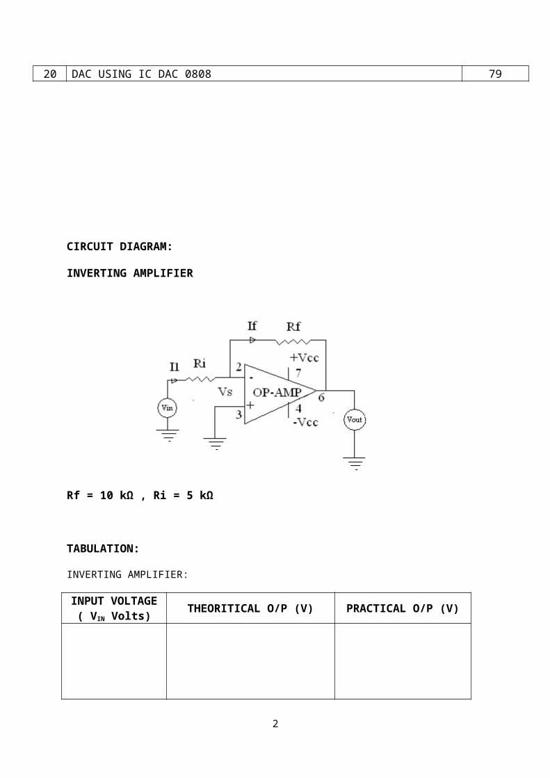
CIRCUIT DIAGRAM:
INVERTING AMPLIFIER
Rf = 10 kΩ , Ri = 5 kΩ
TABULATION:
INVERTING AMPLIFIER:
INPUT VOLTAGE ( VIN Volts)
THEORITICAL O/P (V) PRACTICAL O/P (V)
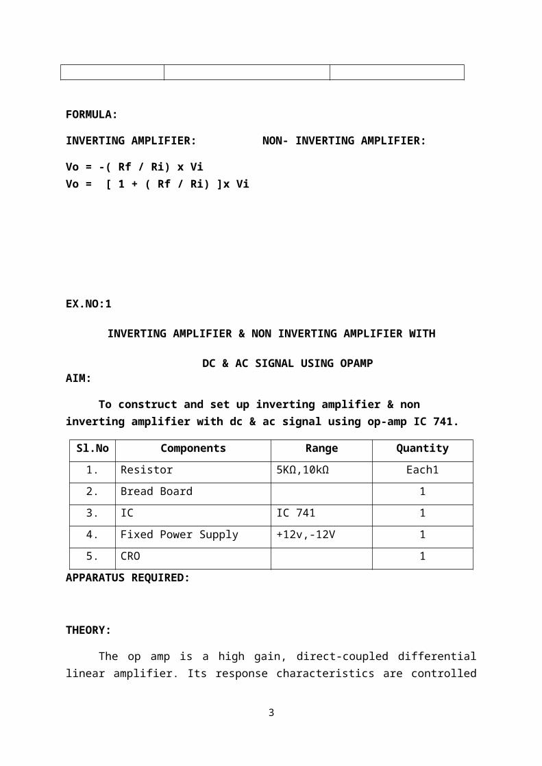
FORMULA:
INVERTING AMPLIFIER: NON- INVERTING AMPLIFIER:
Vo = -( Rf / Ri) x Vi Vo = [ 1 + ( Rf / Ri) ]x Vi
EX.NO:1
2
INVERTING AMPLIFIER & NON INVERTING AMPLIFIER WITH
DC & AC SIGNAL USING OPAMPAIM:
To construct and set up inverting amplifier & non inverting amplifier with dc & ac signal using op-amp IC 741.
Sl.No Components Range Quantity
1. Resistor 5KΩ,10kΩ Each1
2. Bread Board 1
3. IC IC 741 1
4. Fixed Power Supply +12v,-12V 1
5. CRO 1
APPARATUS REQUIRED:
THEORY:
The op amp is a high gain, direct-coupled differential linear amplifier. Its response characteristics are controlled by external negative feedback from output to input. They are widely used in all phased of electronics.
Negative input is the inverting input. When the signal is applied to this input, the output is 180° out of phase with the input. The +(plus) input is non-inverting. The output is in phase with the input when the input is applied to this terminal. One other importance fact about the op amp: Most require a dual power source, although some units operate satisfactorily with a single supply.
PROCEDURE:
1. The Connections are given as shown in the circuit diagram. 2. Excitation voltage of +12V and -12V from regulated power supply is connected to Operational Amplifier terminals 7 & 4. 3. The corresponding input voltage are given and the output voltage are measured.
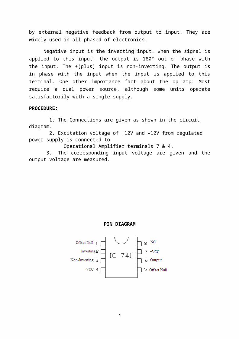
PIN DIAGRAM
3
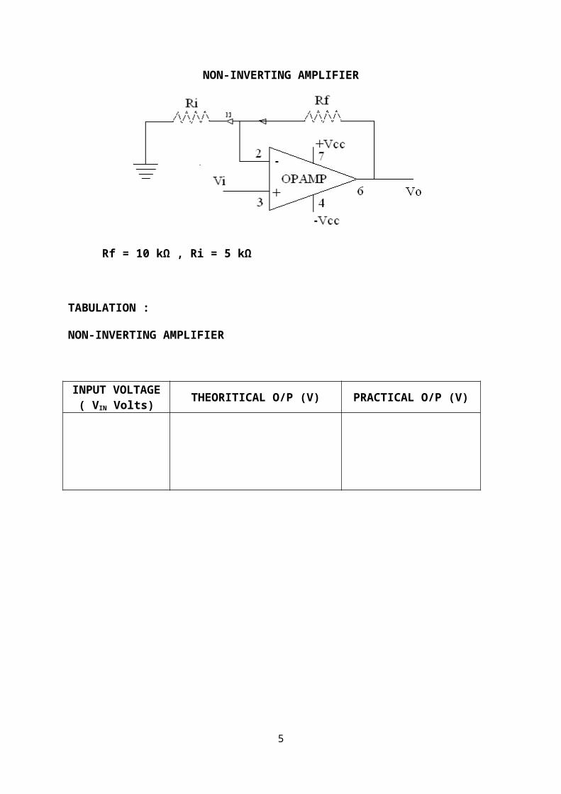
NON-INVERTING AMPLIFIER
Rf = 10 kΩ , Ri = 5 kΩ
TABULATION :
NON-INVERTING AMPLIFIER
INPUT VOLTAGE ( VIN Volts)
THEORITICAL O/P (V) PRACTICAL O/P (V)
4
RESULT:
Thus the inverting amplifier, Non-inverting amplifier are designed using IC 741 and their performance are tested.
CIRCUIT DIAGRAM:
5
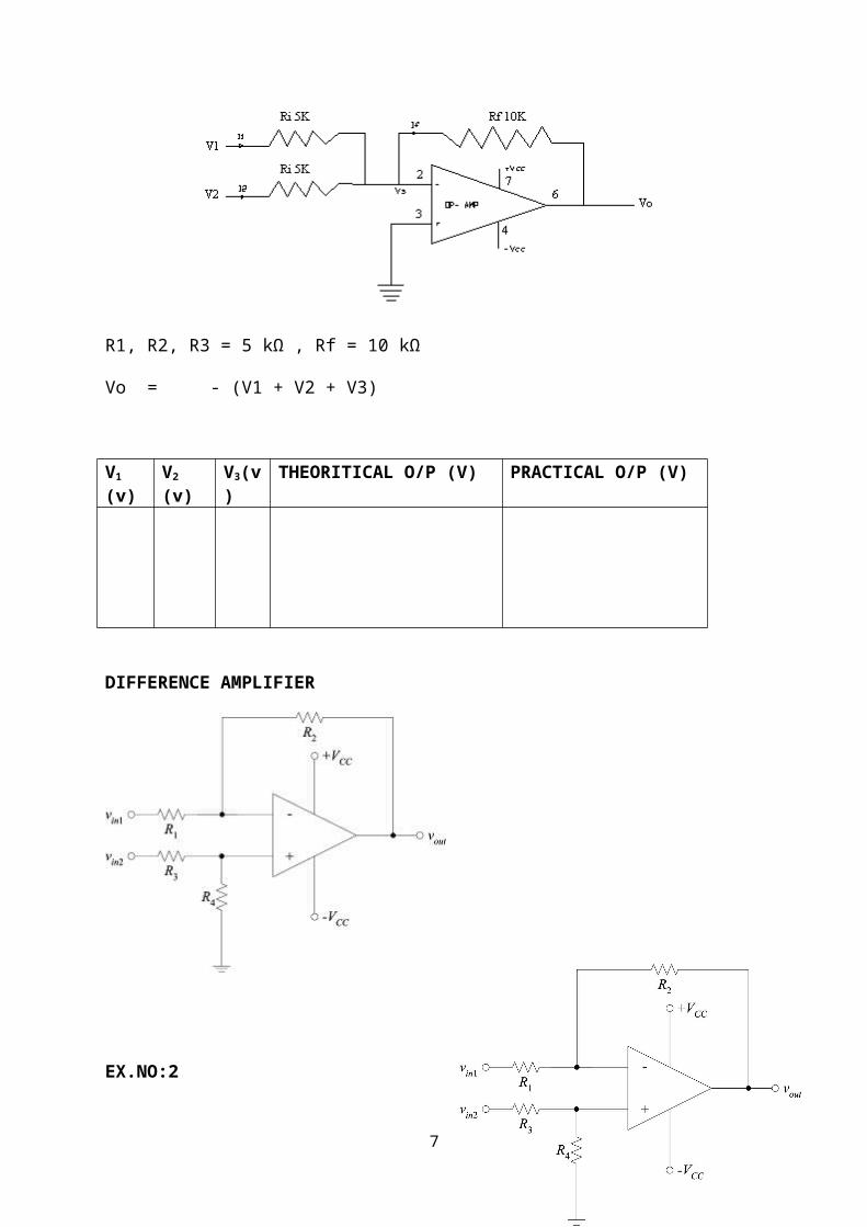
SUMMING AMPLIFIER
R1, R2, R3 = 5 kΩ , Rf = 10 kΩ
Vo = - (V1 + V2 + V3)
V1 (v) V2 (v) V3(v) THEORITICAL O/P (V) PRACTICAL O/P (V)
DIFFERENCE AMPLIFIER
EX.NO:2
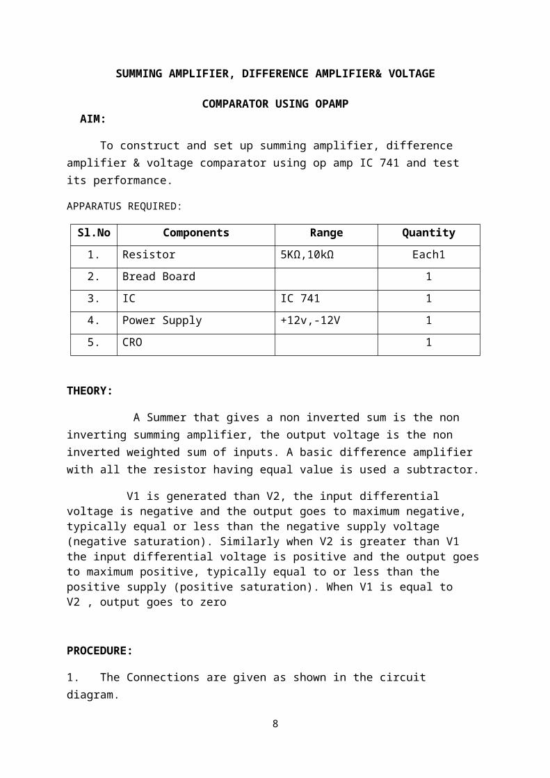
SUMMING AMPLIFIER, DIFFERENCE AMPLIFIER& VOLTAGE
6
COMPARATOR USING OPAMP AIM:
To construct and set up summing amplifier, difference amplifier & voltage comparator using op amp IC 741 and test its performance.
APPARATUS REQUIRED:
Sl.No Components Range Quantity
1. Resistor 5KΩ,10kΩ Each1
2. Bread Board 1
3. IC IC 741 1
4. Power Supply +12v,-12V 1
5. CRO 1
THEORY:
A Summer that gives a non inverted sum is the non inverting summing amplifier, the output voltage is the non inverted weighted sum of inputs. A basic difference amplifier with all the resistor having equal value is used a subtractor.
V1 is generated than V2, the input differential voltage is negative and the output goes to maximum negative, typically equal or less than the negative supply voltage (negative saturation). Similarly when V2 is greater than V1 the input differential voltage is positive and the output goes to maximum positive, typically equal to or less than the positive supply (positive saturation). When V1 is equal to V2 , output goes to zero
PROCEDURE:
1. The Connections are given as shown in the circuit diagram.
2. Excitation voltage of +12V and -12V from regulated power supply is connected to Operational Amplifier terminals 7 & 4.
3. The corresponding input voltage are given and the output voltage are measured.
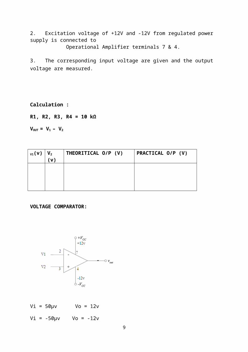
Calculation :
R1, R2, R3, R4 = 10 kΩ
VOUT = V1 – V2
7
V1(v) V2 (v) THEORITICAL O/P (V) PRACTICAL O/P (V)
VOLTAGE COMPARATOR:
Vi = 50µv Vo = 12v
Vi = -50µv Vo = -12v
FORMULA:
Summing Vo = [ 1+ Rf / Ri ] x [ (V1/R1) + (V2/R2) + (V3/R3) / (1/R1) + (1/R2) + (1/R3) ]
Difference Vo = [R2 / R1] (V1-V2) When R2=R1
8
RESULT:
Thus the summing amplifier, difference amplifier & voltage comparator using op amp IC 741 is constructed and their performance are tested.
EX.NO:3
CIRCUIT DIAGRAM:
9

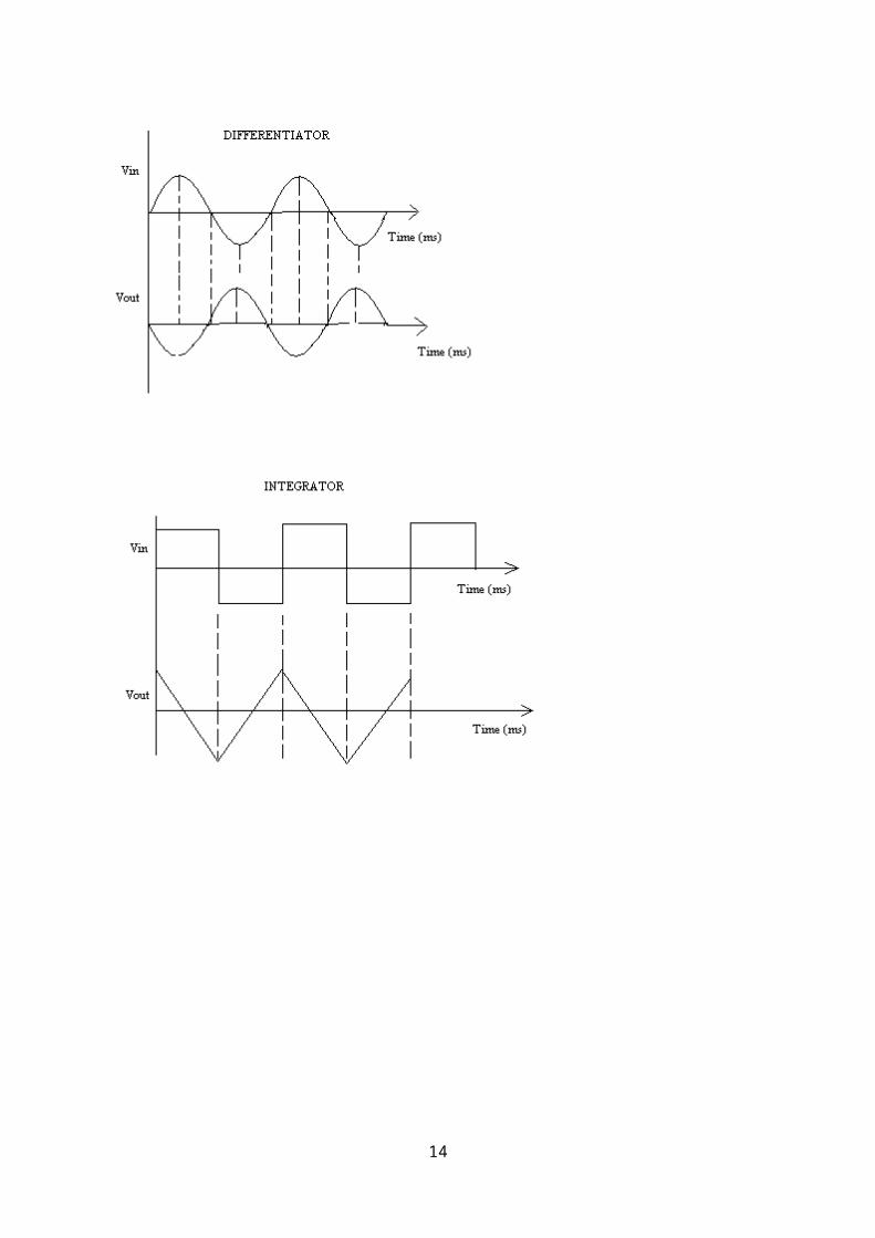
DIFFERENTIATOR:
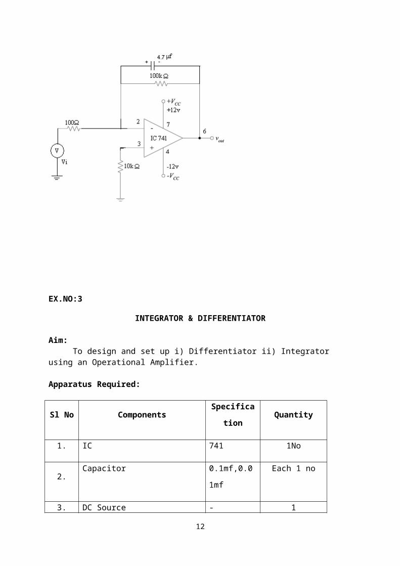
INTEGRATOR:
EX.NO:3
INTEGRATOR & DIFFERENTIATOR
Aim:
10
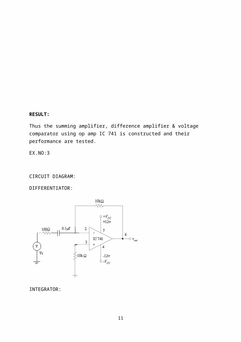
To design and set up i) Differentiator ii) Integrator using an Operational Amplifier.
Apparatus Required:
Sl No Components Specification Quantity
1. IC 741 1No
2. Capacitor 0.1mf,0.01mf Each 1 no
3. DC Source - 1
4. Resistor 10K,100 K Each 1 no
5. Function Generator - 1
6. CRO - 1
Procedure: 1.Set the circuit after verifying the condition of the IC using analog tester or by voltage follower
circuit.
2. Give input and output waveforms.
11
12
Result:
Thus the integrator and differentiator circuits were constructed and the output waveforms were studied.
13
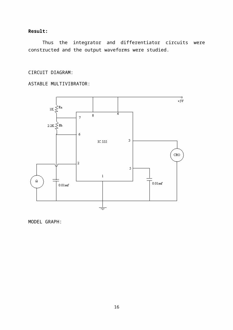
CIRCUIT DIAGRAM:
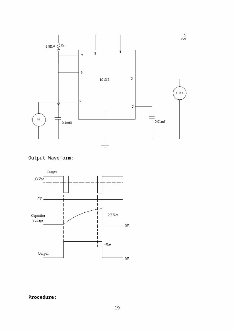
ASTABLE MULTIVIBRATOR:
MODEL GRAPH:
14

EX.NO:4
ASTABLE & MONOSTABLE MULTIVIBRATOR USING IC 555
Aim:
To Construct and test the performance of Astable and monostable Multivibrator using IC 555.
Apparatus Required:
Sl No Description Range Quantity
1. Timer IC 555 1No
2. Capacitor 1000mf,0.01mf 1,2
3. IC Power Supply +5V 1
4. Resistor 1K,10 K,2.2K,22K Each 1 no
5. Function Generator 1Mhz 1
6. CRO 20Mhz 1
7. Bread Board - 1
Procedure:
Astable Multivibrator:
1. The circuit is rigged upto the group board as per the connection diagram given.
2. A Supply of +5V is given from the RPS to the circuit.
3. The oscilloscope is connected at the output terminals the waveform is observed and recorded.
4. The time for ON and OFF period are noted clesrly
Calculation:
T= 0.69 [Ra+2Rb] C Seconds
F= 1/T hz
15
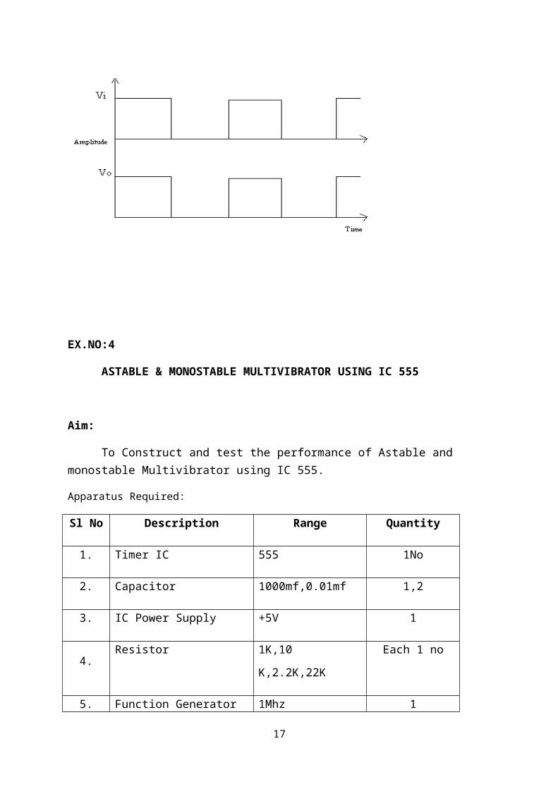
MONOSTABLE MULTIVIBRATOR:
Output Waveform:
16
Procedure:
Monostable Multivibrator:
1. The circuit is rigged up to the group board as per the connection diagram given.
2. A Supply of +5V is given from the RPS to the circuit.
3. Triggering is applied by pressing the push button.
4. Note the LED connected at the output terminal as shown as the switch pressed.
5. Note the duration of the time during which LED glows.
6. Verify timing obtain with the theoretical timing obtained by the application of timing formula
Calculation:
Tp = 1.1xRxC Sec
Result:
Thus the Astable and Monostable from the above calculation the theoretical trigger is rectified with the practical trigger of 555 IC.
17
IC 7805
IC7912
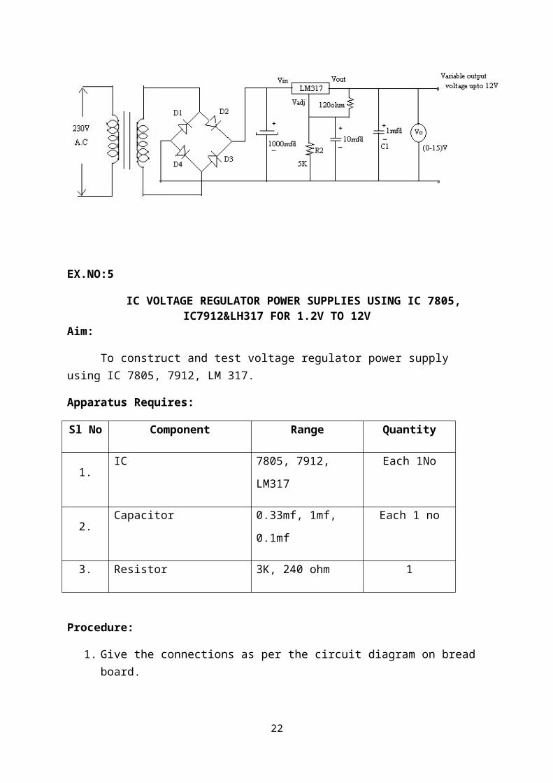
LM317 Voltage Regulator Circuit:
18
EX.NO:5
IC VOLTAGE REGULATOR POWER SUPPLIES USING IC 7805, IC7912&LH317 FOR 1.2V TO 12V
Aim:
To construct and test voltage regulator power supply using IC 7805, 7912, LM 317.
Apparatus Requires:
Sl No Component Range Quantity
1. IC 7805, 7912, LM317 Each 1No
2. Capacitor 0.33mf, 1mf, 0.1mf Each 1 no
3. Resistor 3K, 240 ohm 1
Procedure:
1. Give the connections as per the circuit diagram on bread board.
2. The unregulated voltage is given as input & for the difference settings the regulated voltage is taken at output are tabulated.
19

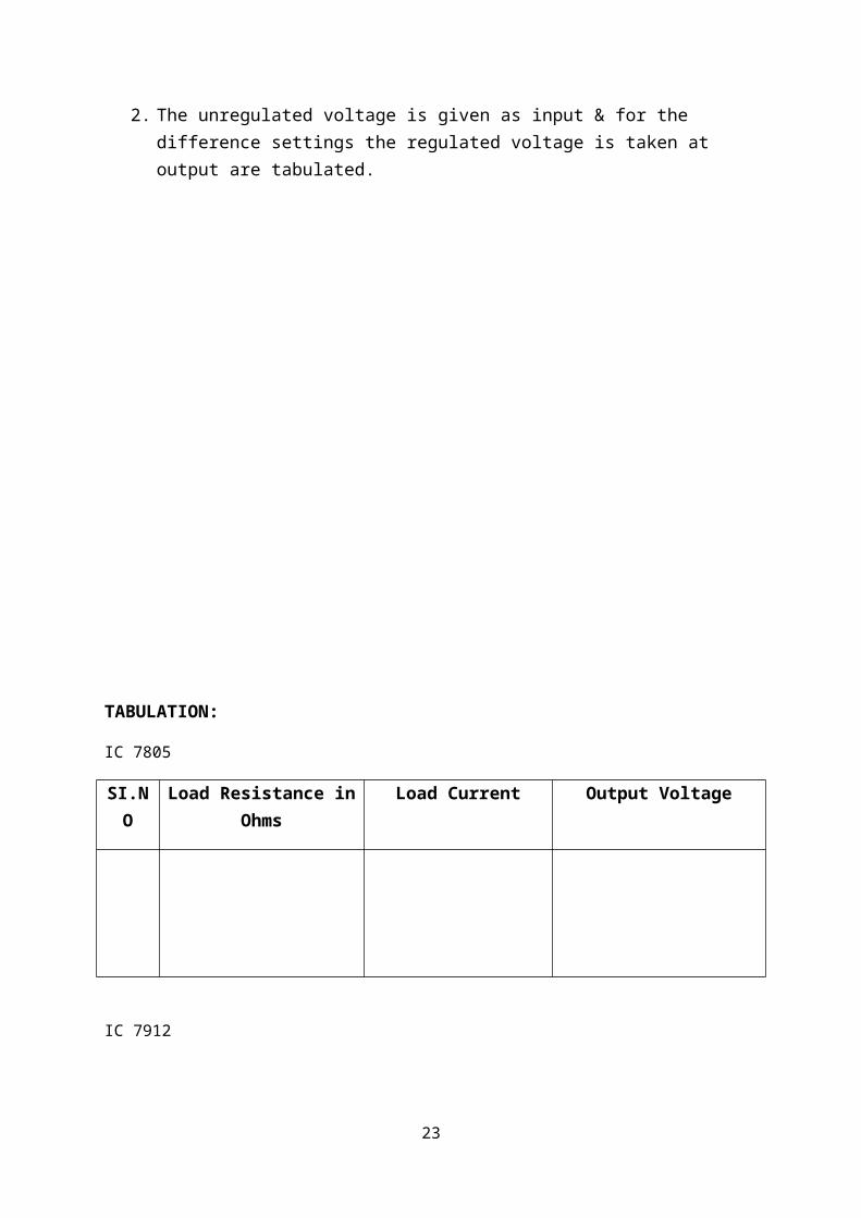
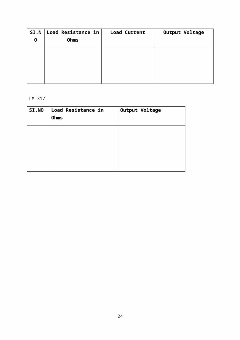
TABULATION:
IC 7805
SI.NO Load Resistance in Ohms Load Current Output Voltage
IC 7912
SI.NO Load Resistance in Ohms Load Current Output Voltage
LM 317
SI.NO Load Resistance in Ohms Output Voltage
20
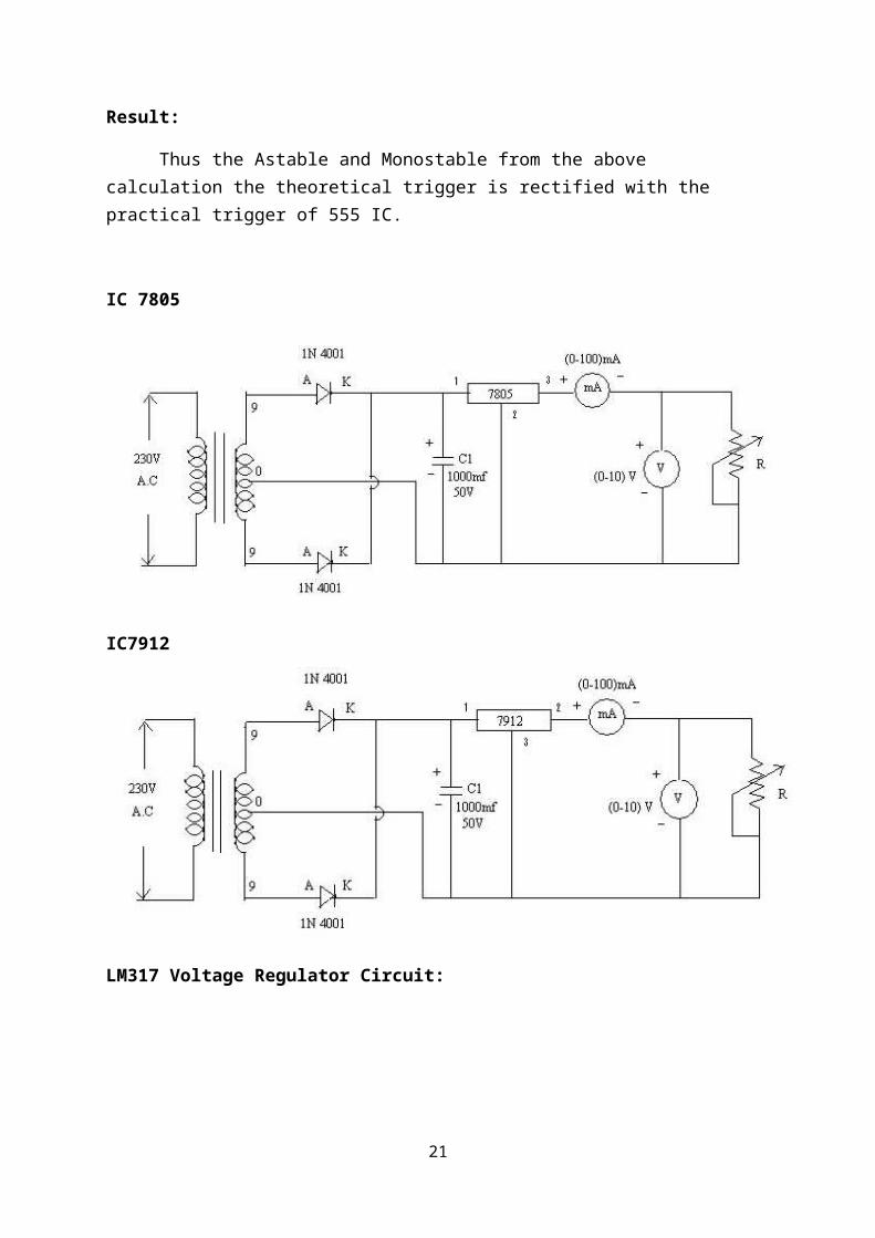
Result:
Thus the voltage regulator power supplies using IC 7805, 7912, LM =317 are constructed, tested and the readings are tabulated.
21
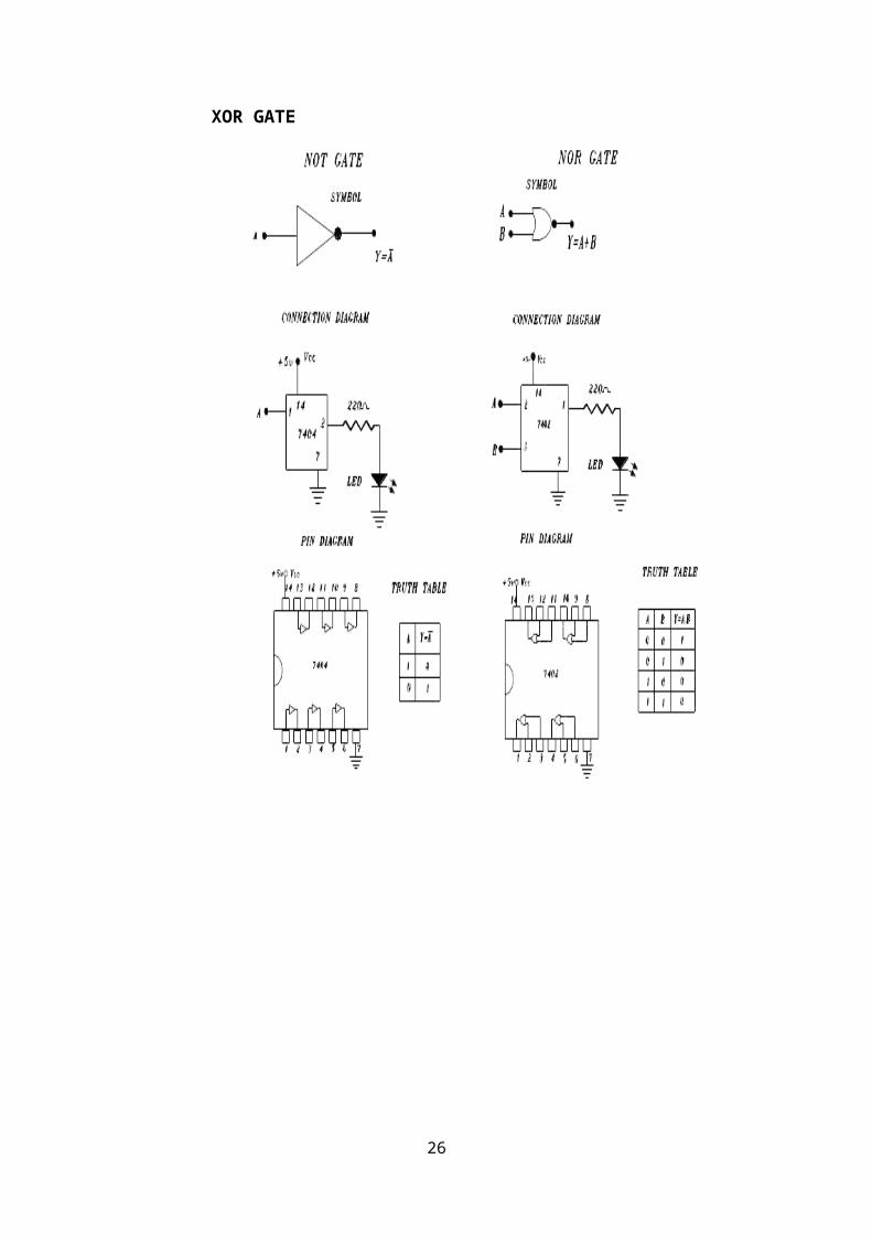
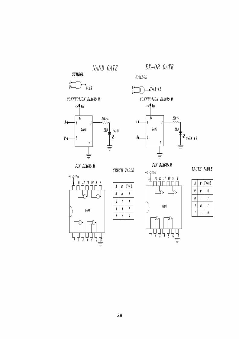
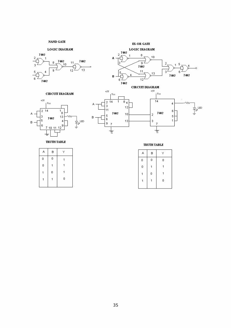
EX.NO:6 VERIFICAION OF TRUTH TABLE OF OR.AND, NOT, NOR, NAND &
XOR GATE
22
EX.NO:6 VERIFICAION OF TRUTH TABLE OF OR.AND, NOT, NOR, NAND &
XOR GATE
Aim:
To verify the truth table of the following logic gates using IC 74xx (i)OR gate (ii) AND gate (iii) NOT gate (iv) NOR gate (iv) NAND gate (v) Ex-OR gate.
Apparatus Required:
Sl No Components Quantity
1. IC 7408,IC 7432,IC 7404,
IC 7400,IC7402&IC 7486
Each 1No
2. Trainer Kit 1No
3. Connecting wires As required
Procedure:
1. Connections are made as per the Circuit diagram.
2. The supply voltage +5v is given to the IC.
3. Inputs are applied to the proper pins of the IC.
4. Output for different input conditions is verified as shown in the truth table.
5. The same procedure is repeated for all the above mentioned ICs.
23
24

Result:
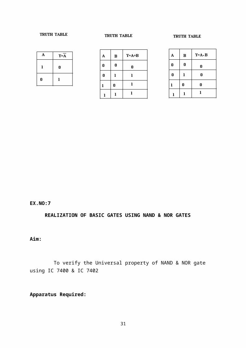
Thus the truth tables of OR, NOT, NOR, AND, NAND&EX-OR gates are verified using ICs 7432, 7404,7402,7408,7400 & 7486 respectively.
25
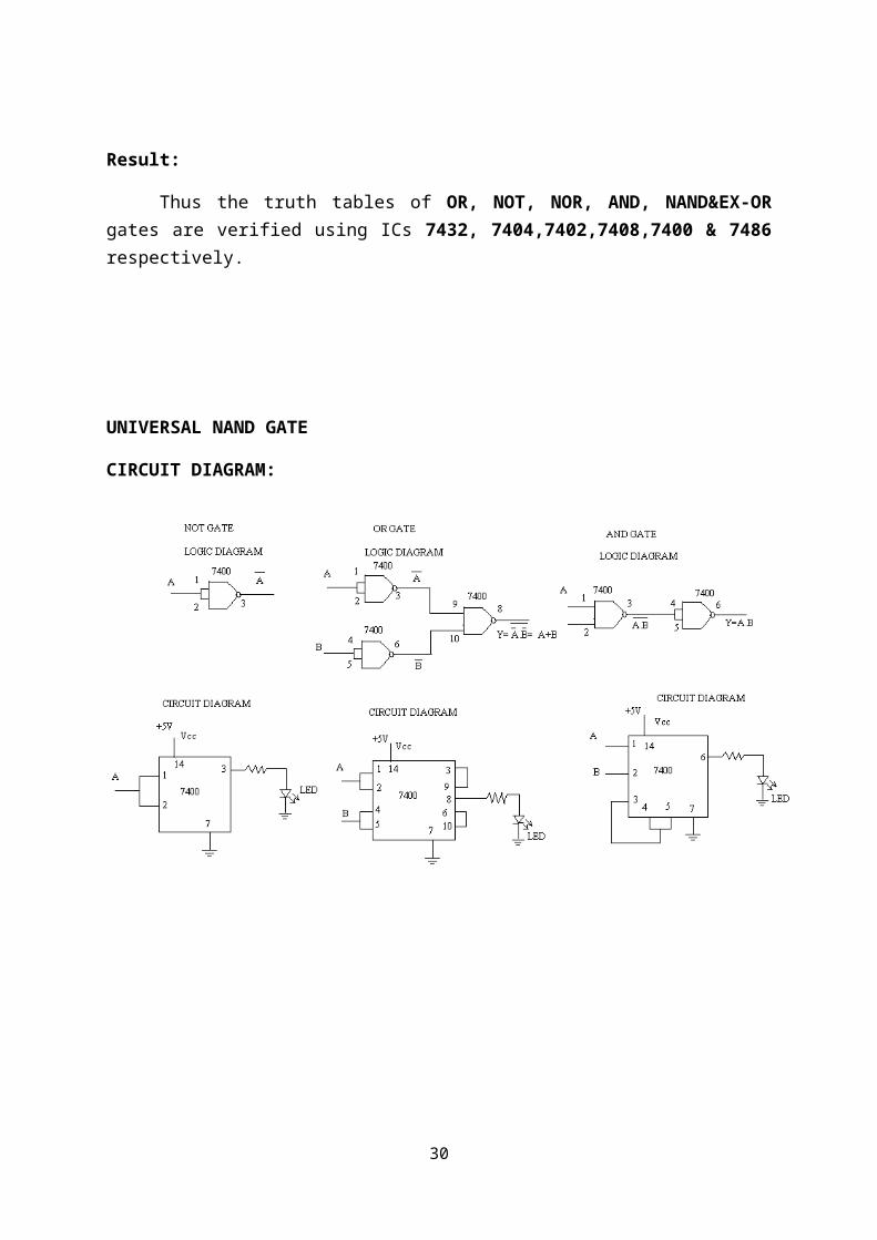
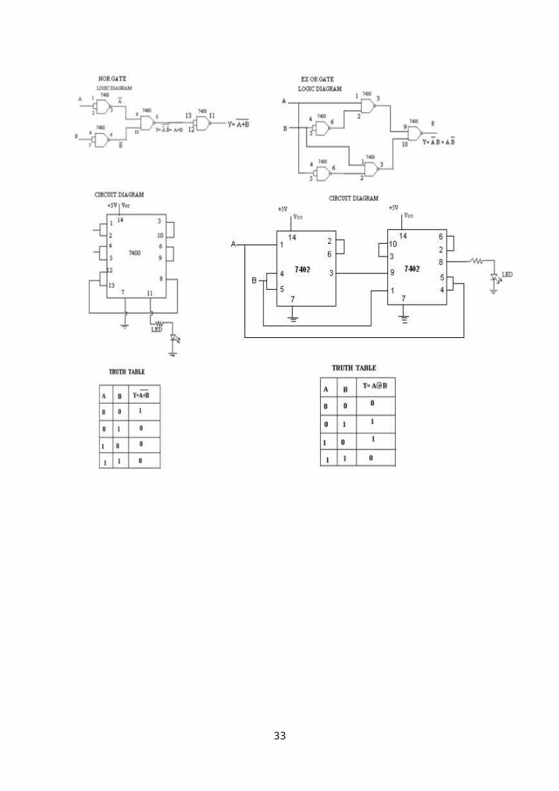
UNIVERSAL NAND GATE
CIRCUIT DIAGRAM:
26
EX.NO:7
REALIZATION OF BASIC GATES USING NAND & NOR GATES
Aim:
To verify the Universal property of NAND & NOR gate using IC 7400 & IC 7402
Apparatus Required:
Sl.No Components Quantity
1. IC 7400, IC 7402 2 Nos
2. Trainer Kit 1No
3. Connecting wires As required
Procedure:
1. Connections are made as per the Circuit diagram.
2. The supply voltage +5v is given to the ICs.
3. Inputs are applied to the proper pins of the IC.
4. Outputs for different input conditions are verified as shown in the truth table.
27
28

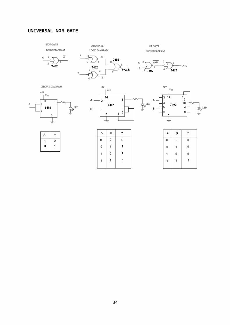
UNIVERSAL NOR GATE
29
30
Result:
Thus the Universal property of NAND gate and NOR gate is verified using IC7400 & IC 7402.
31

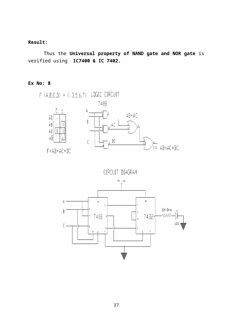
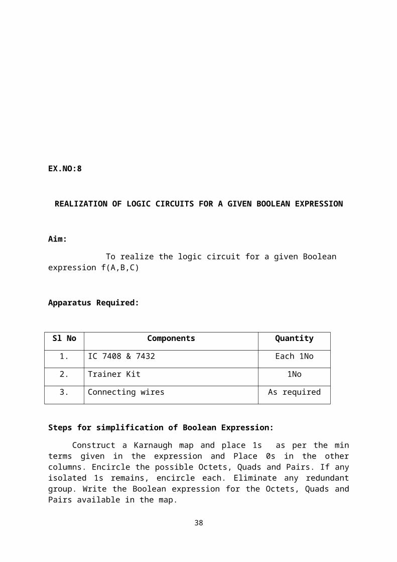
Ex No: 8
32
EX.NO:8
REALIZATION OF LOGIC CIRCUITS FOR A GIVEN BOOLEAN EXPRESSION
Aim:
To realize the logic circuit for a given Boolean expression f(A,B,C)
Apparatus Required:
Sl No Components Quantity
1. IC 7408 & 7432 Each 1No
2. Trainer Kit 1No
3. Connecting wires As required
Steps for simplification of Boolean Expression:
Construct a Karnaugh map and place 1s as per the min terms given in the expression and Place 0s in the other columns. Encircle the possible Octets, Quads and Pairs. If any isolated 1s remains, encircle each. Eliminate any redundant group. Write the Boolean expression for the Octets, Quads and Pairs available in the map.
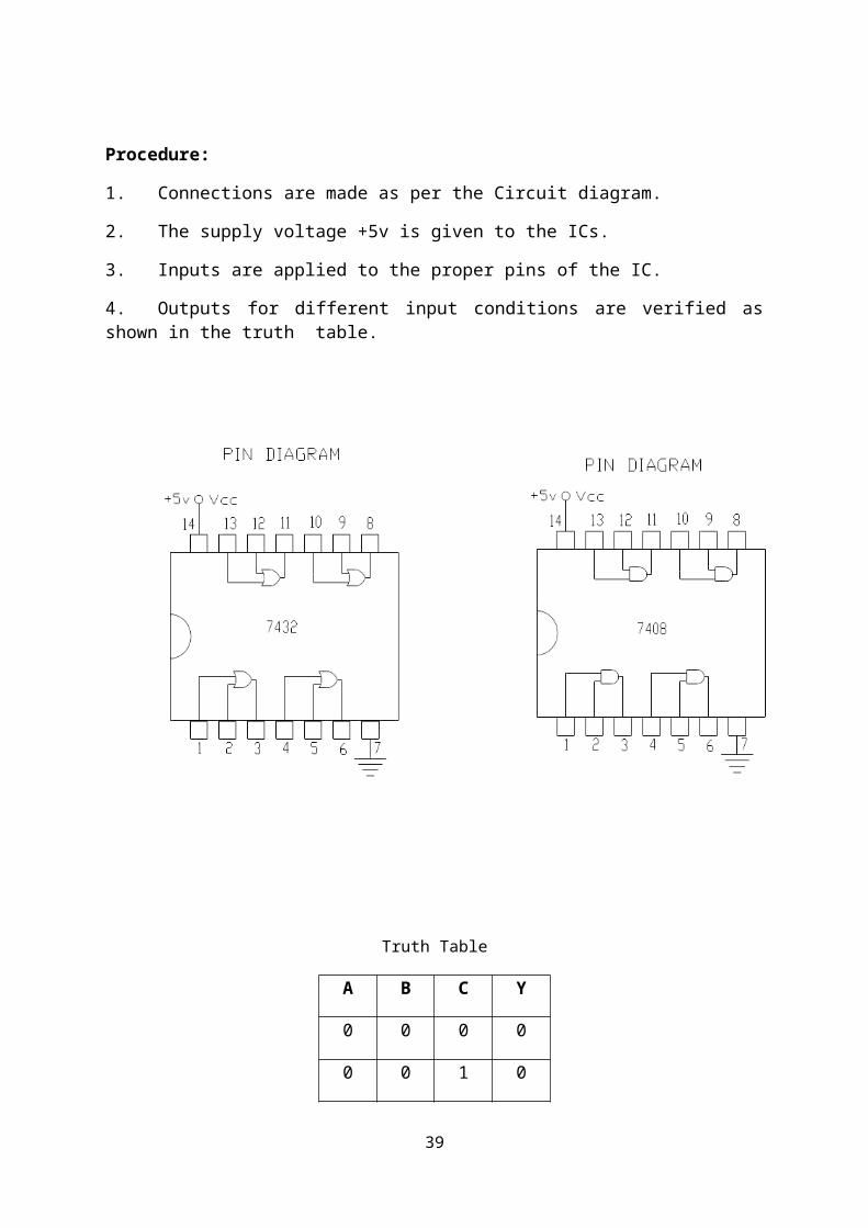
Procedure:
1. Connections are made as per the Circuit diagram.
2. The supply voltage +5v is given to the ICs.
3. Inputs are applied to the proper pins of the IC.
4. Outputs for different input conditions are verified as shown in the truth table.
33
Truth Table
A B C Y
0 0 0 0
0 0 1 0
0 1 0 0
0 1 1 1
1 0 0 0
1 0 1 1
1 1 0 1
1 1 1 1
34
Result:
Thus the circuit for given problem f (A, B, C) is constructed and the truth table is verified.
35

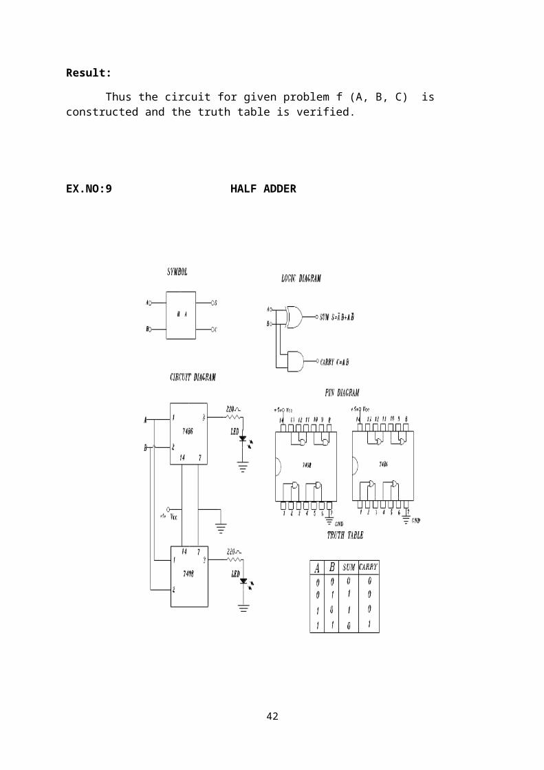
EX.NO:9 HALF ADDER
36
EX.NO:9
HALF ADDER, FULL ADDER AND 4 BIT FULL ADDER USING DISCRETE ICs
Aim:
To construct the Half Adder, Full Adder, 4 Bit full adder circuits using ICs 74xxs and verify the truth table.
Apparatus Required:
Sl No Components Quantity
1. IC 7408, 7432 & IC 7486 Each 1No
2. Trainer Kit 1No
3. Connecting wires As required
Procedure:
1. Connections are made as per the Circuit diagram.
2. The supply voltage +5v is given to the ICs.
3. Inputs are applied to the proper pins of the IC.
4. Outputs for different input conditions are verified as shown in the truth table.
37
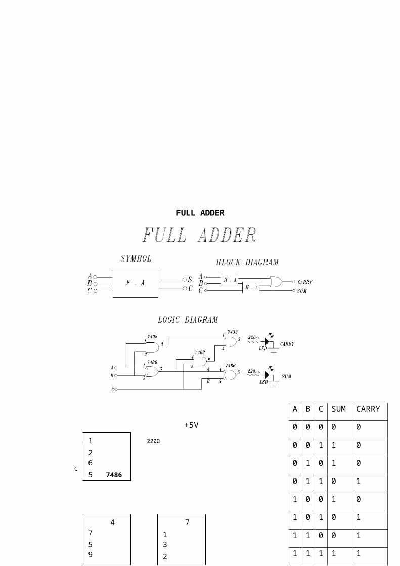
FULL ADDER
+5V
A 220Ω
B
C
220Ω
+5V
38
A B C SUM CARRY
0 0 0 0 0
0 0 1 1 0
0 1 0 1 0
0 1 1 0 1
1 0 0 1 0
1 0 1 0 1
1 1 0 0 1
1 1 1 1 1
1 2 65 7486
3 4 7
4 75 9 1 7408 62 14
71 32 7432
14
Result:
Thus the Half Adder,Full Adder and 4 bit full adder is constructed using 7408,7486 and 7432 ICs and the truth table is verified.
39

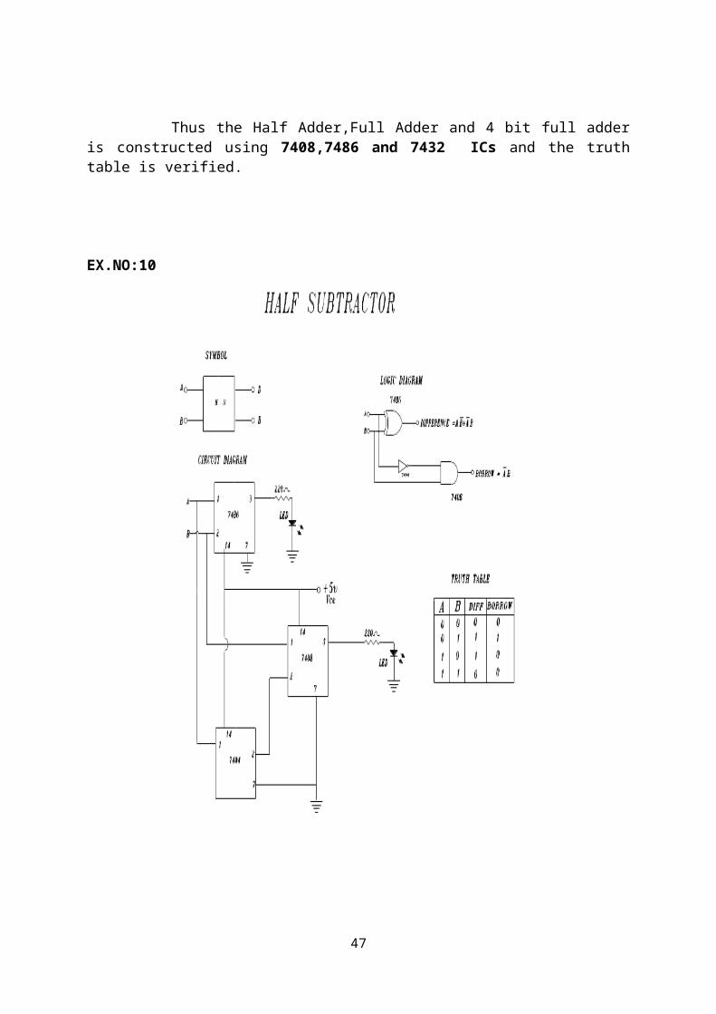
EX.NO:10
40

EX.NO:10
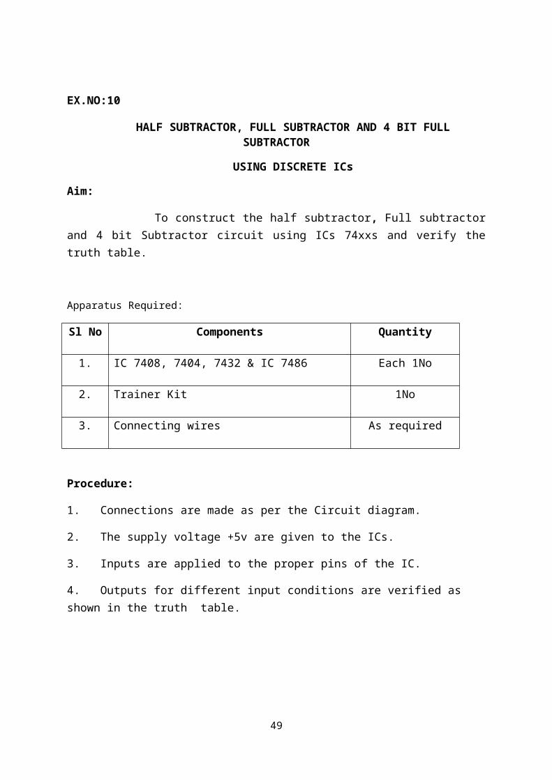
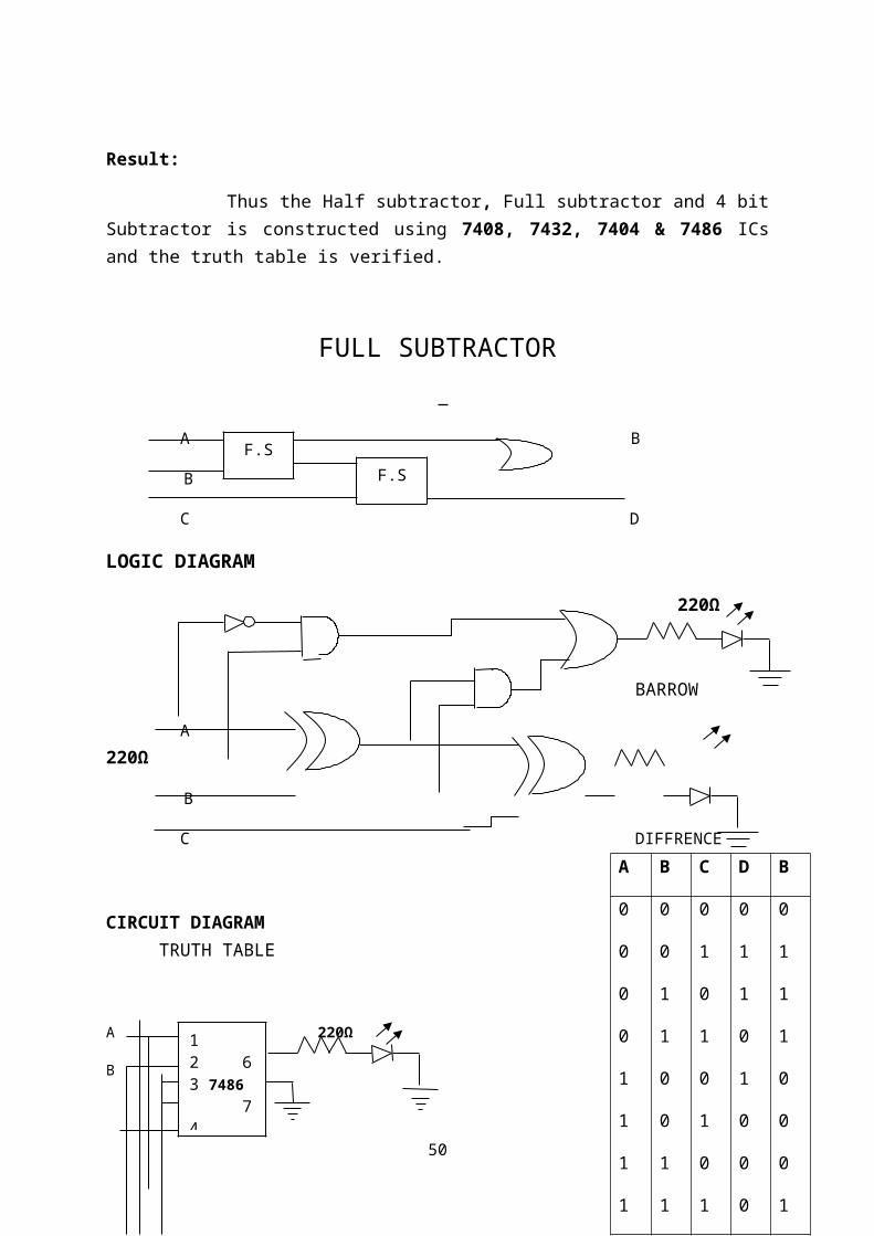
HALF SUBTRACTOR, FULL SUBTRACTOR AND 4 BIT FULL SUBTRACTOR
USING DISCRETE ICs
Aim:
To construct the half subtractor, Full subtractor and 4 bit Subtractor circuit using ICs 74xxs and verify the truth table.
Apparatus Required:
Sl No Components Quantity
1. IC 7408, 7404, 7432 & IC 7486 Each 1No
2. Trainer Kit 1No
3. Connecting wires As required
Procedure:
1. Connections are made as per the Circuit diagram.
2. The supply voltage +5v are given to the ICs.
3. Inputs are applied to the proper pins of the IC.
4. Outputs for different input conditions are verified as shown in the truth table.
Result:
Thus the Half subtractor, Full subtractor and 4 bit Subtractor is constructed using 7408, 7432, 7404 & 7486 ICs and the truth table is verified.
41
FULL SUBTRACTOR
A B
B
C D
LOGIC DIAGRAM
220Ω
BARROW
A 220Ω
B
C DIFFRENCE
CIRCUIT DIAGRAM TRUTH TABLE
A 220Ω
B
C +5v
220Ω
42
A B C D B
0
0
0
0
1
1
1
1
0
0
1
1
0
0
1
1
0
1
0
1
0
1
0
1
0
1
1
0
1
0
0
0
0
1
1
1
0
0
0
1
F.S
F.S
1 2 63 7486 74 5 14
1 14 2
7404 4
3 7
1 14 32 7408 4 65 7
1 14 3
2 7432
7
Result:
Thus the Half subtractor, Full subtractor and 4 bit Subtractor is constructed using 7408, 7432, 7404 & 7486 ICs and the truth table is verified.
43
EX.NO:11
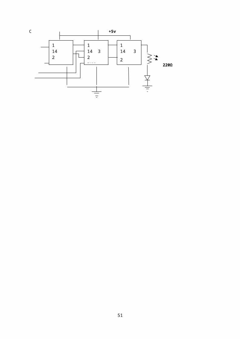
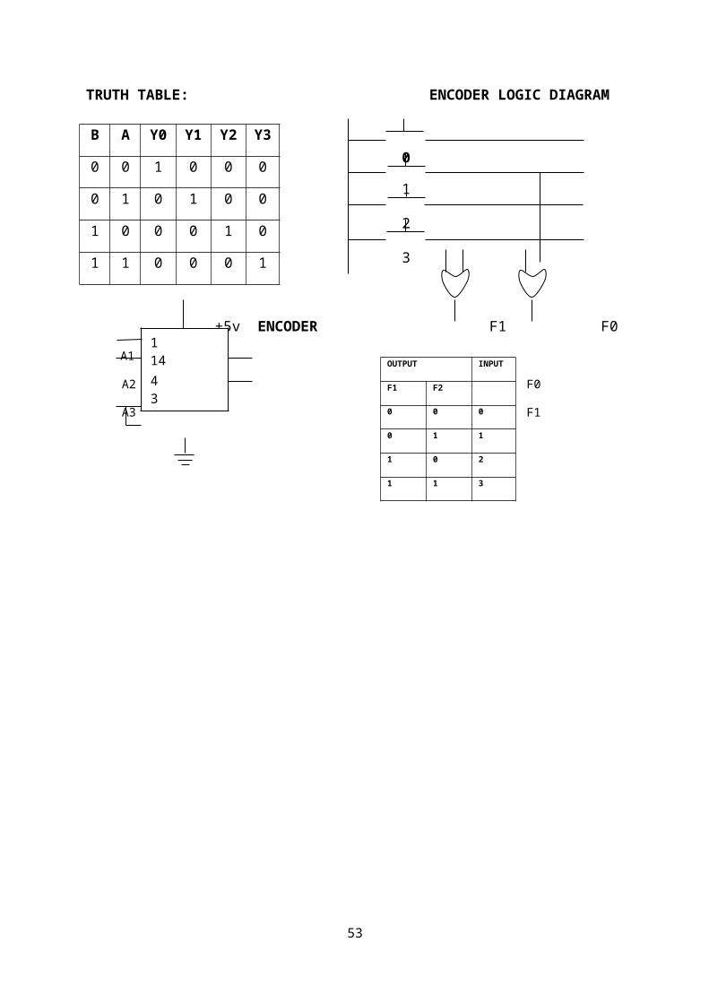
TRUTH TABLE: ENCODER LOGIC DIAGRAM
0
1
2
3
+5v ENCODER F1 F0
A1
A2 F0
A3 F1
44
B A Y0 Y1 Y2 Y3
0 0 1 0 0 0
0 1 0 1 0 0
1 0 0 0 1 0
1 1 0 0 0 1
OUTPUT INPUT
F1 F2
0 0 0
0 1 1
1 0 2
1 1 3
1 144 32 7432 65

EX.NO:11
CONSTRUCTION AND VERIFICATION OF TRUTH TABLE FOR
DECODER, ENCODER
Aim:
To construct the Decoder and Encoder circuits using ICs 74xx and verify the truth table.
Apparatus Required:
Sl No Components Quantity
1. IC 7408, IC 7404 & IC 7432 Each 1No
2. Trainer Kit 1No
3. Connecting wires As required
THEORY :
Decoder :
It is a device which does the reverse of an encoder, undoing the encoding so that the original information can be retrieved. The same method used to encode is usually just reversed in order to decode
Encoder :
A single bit 4 to 2 encoder takes in 4 bits and outputs 2 bits. It is assumed that there are only 4 types of input signals: 0001, 0010, 0100, 1000
Procedure:
1. Connections are made as per the Circuit diagram.
2. The supply voltage +5v is given to the ICs.
3. Inputs are applied to the proper pins of the IC.
4. Outputs for different input conditions are verified as shown in the truth table.
Result:
Thus the Decoder, Encoder is constructed using 7408, 7404, & 7432 ICs and the truth table is verified.
45

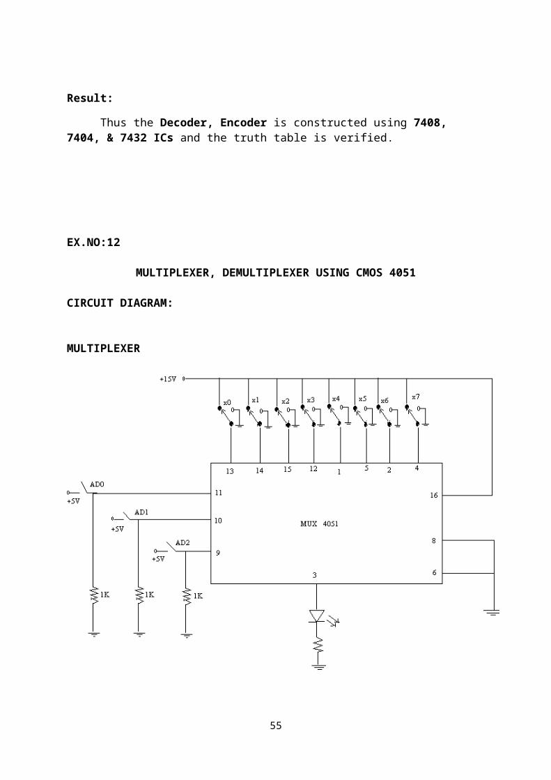
EX.NO:12
MULTIPLEXER, DEMULTIPLEXER USING CMOS 4051
CIRCUIT DIAGRAM:
MULTIPLEXER
46
EX.NO:12
MULTIPLEXER, DEMULTIPLEXER USING CMOS 4051
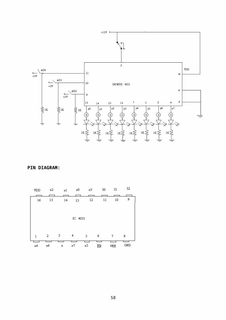
AIM:
To Study the operation of a Multiplexer, De multiplexer Using CMOS 4051
THEORY:
Multiplexer:
Multiplexer means many in to one
A digital multiplexer is a combinational circuit that selects binary information from one of several input lines and directs it to a single line for transmission to a common destination the selection of a particular four input line is controlled by a set of selected lines. The multiplexer has several data input lines and a single output line. It also have data selected input that helps to choose any one of the inputs to be switched to the output line.
De multiplexer:
A demultiplexer performs the reverse axtion of a multiplexer it takes data from one line and distributes it to a given number of output lines. Thus Demux has one input and many output.
Procedure:
1. Connections are made as per the Circuit diagram.
2. The supply voltage +5v is given to the ICs.
3. Clock pulse is applied to the proper pin of the IC.
4. Outputs for different input conditions are verified as shown in the truth table.
47

DEMULTIPLEXER:
PIN DIAGRAM:
48
Result:
Thus the function of multiplexer and de multiplexer are verified.
49
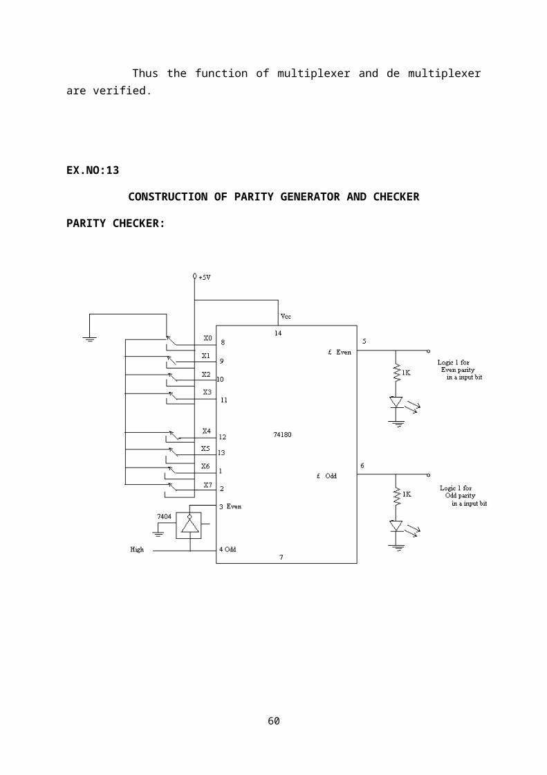
EX.NO:13
CONSTRUCTION OF PARITY GENERATOR AND CHECKER
PARITY CHECKER:
50
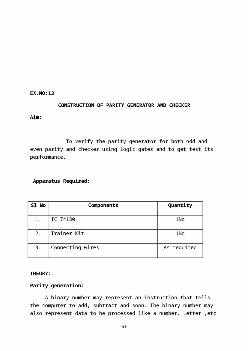
EX.NO:13
CONSTRUCTION OF PARITY GENERATOR AND CHECKER
Aim:
To verify the parity generator for both odd and even parity and checker using logic gates and to get test its performance.
Apparatus Required:
Sl No Components Quantity
1. IC 74180 1No
2. Trainer Kit 1No
3. Connecting wires As required
THEORY:
Parity generation:
A binary number may represent an instruction that tells the computer to add, subtract and soon. The binary number may also represent data to be processed like a number. Letter ,etc in a computer. In either case an extra bit is added to the original binary number to produce a binary number with even or odd parity. Such an extra parity bit can be earily generated using an EX-OR gate.
Parity checking:
Parity checking is nothing but checking the even parity or odd parity of binary word which is used for transmission of data one place to another place in a digital system. The parity checking is also performed by using XOR logic diagram.
For parity checking and generation a TTL IC 74180 is designed and used in parity application.
51
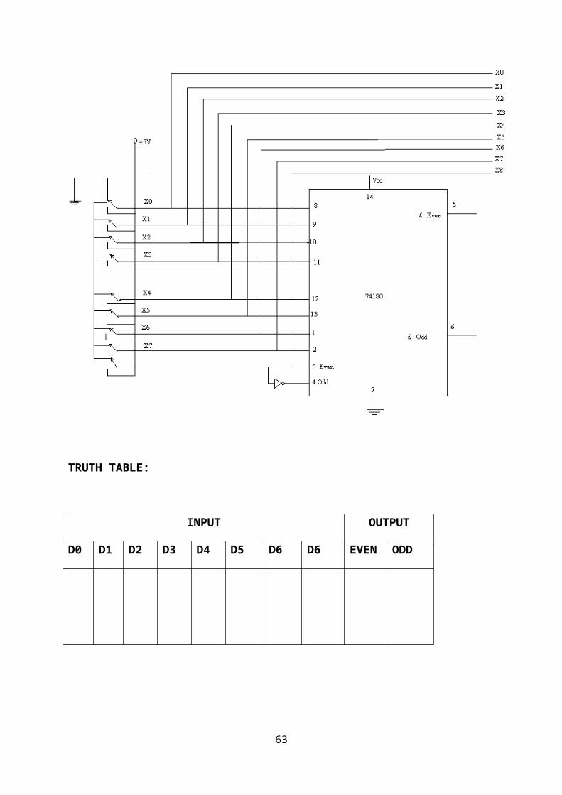
PARITYGENERATOR:
TRUTH TABLE:
INPUT OUTPUT
D0 D1 D2 D3 D4 D5 D6 D6 EVEN ODD
52
Procedure:
1. Connections are made as per the Circuit diagram.
2. The supply voltage +5v is given to the ICs.
3. Clock pulse is applied to the proper pin of the IC.
4. Outputs for different input conditions are verified as shown in the truth table.
Result:
Thus the parity generator and parity checker performences are verified.
53

EX.NO:14
54
EX.NO:14
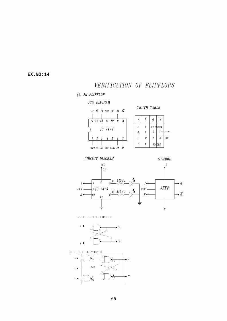
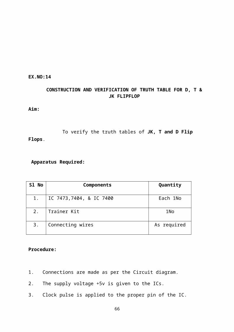
CONSTRUCTION AND VERIFICATION OF TRUTH TABLE FOR D, T & JK FLIPFLOP
Aim:
To verify the truth tables of JK, T and D Flip Flops.
Apparatus Required:
Sl No Components Quantity
1. IC 7473,7404, & IC 7400 Each 1No
2. Trainer Kit 1No
3. Connecting wires As required
Procedure:
1. Connections are made as per the Circuit diagram.
2. The supply voltage +5v is given to the ICs.
3. Clock pulse is applied to the proper pin of the IC.
4. Outputs for different input conditions are verified as shown in the truth table.
55
T FLIPFLOP (a) Logic Circuit (b) Graphical symb
(c) Truth table
56

Result:
Thus the truth tables JK FlipFlop, T FlipFlop and D Flipflop are verified.
57
EX.NO:15
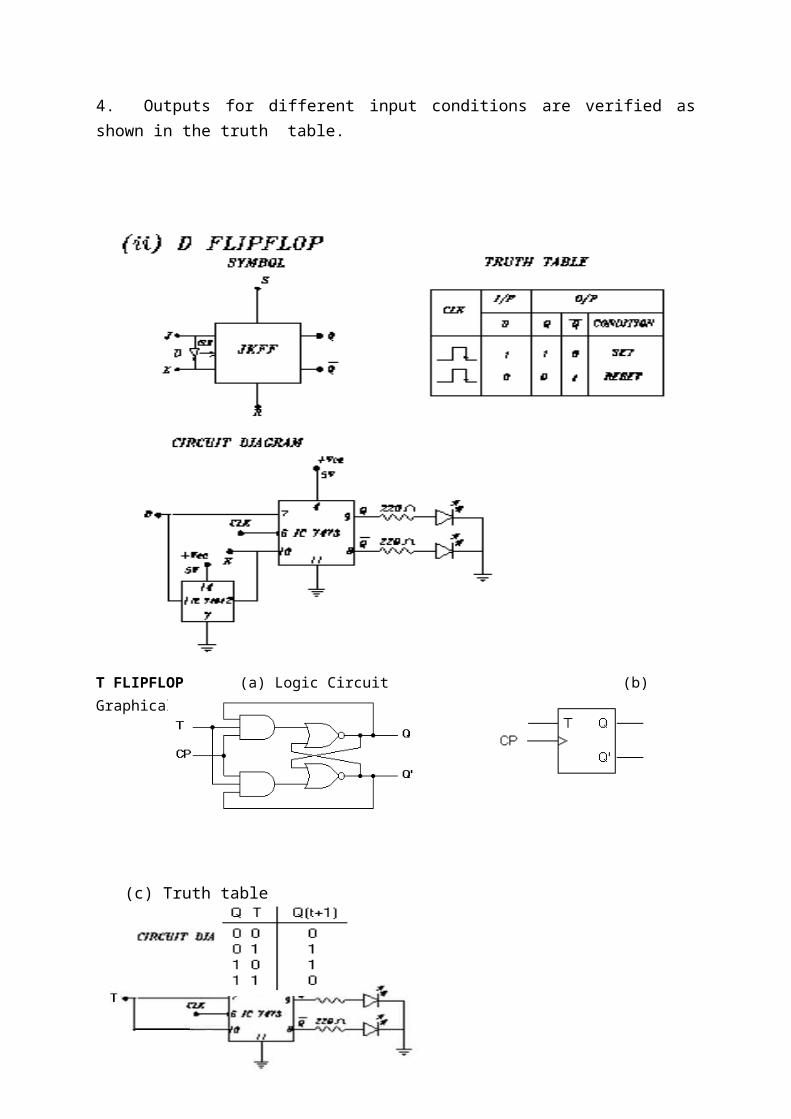
4 BIT RIPPLE COUNTER USING FLIP FLOP WITH FEEDBACK
CIRCUIT DIAGRAM:
+5v
CLK
PIN DIAGRAM:
58
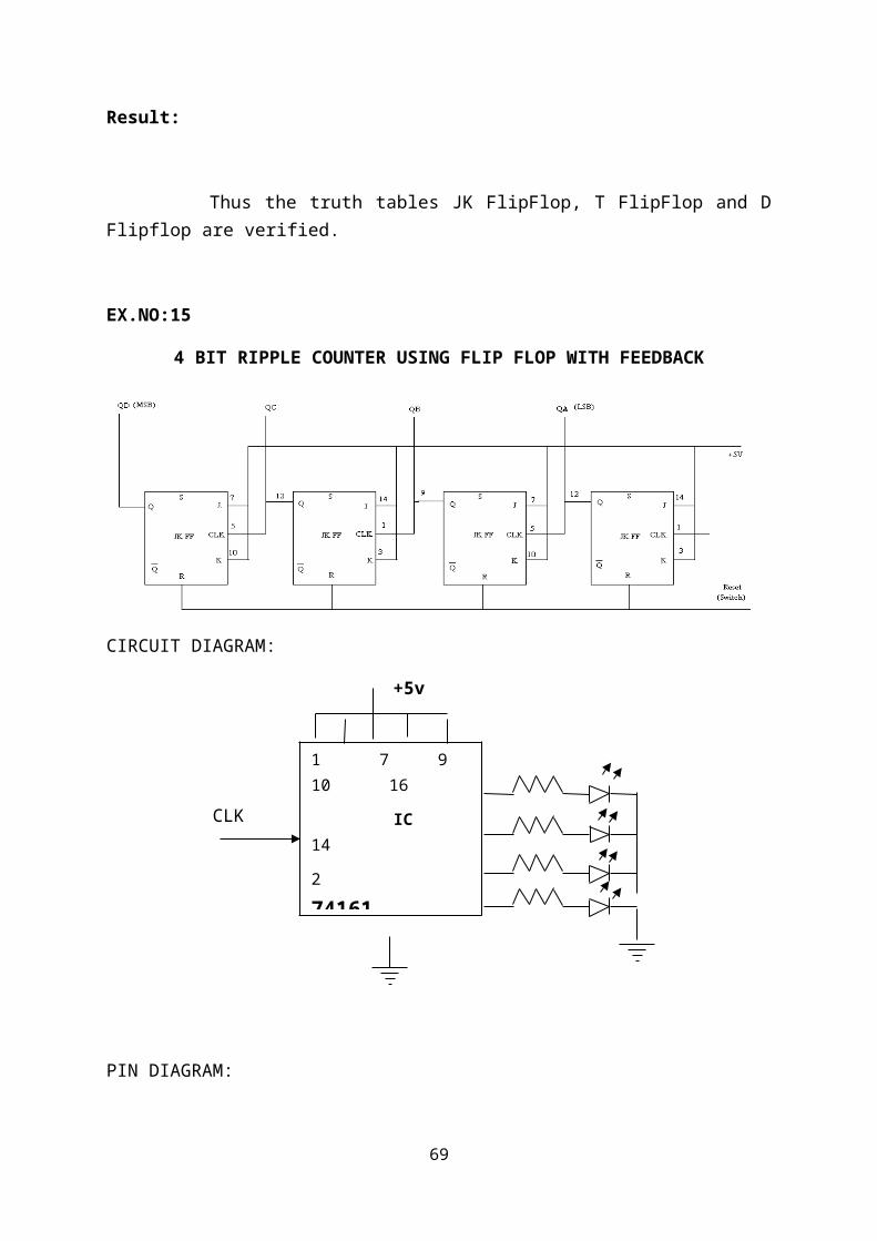
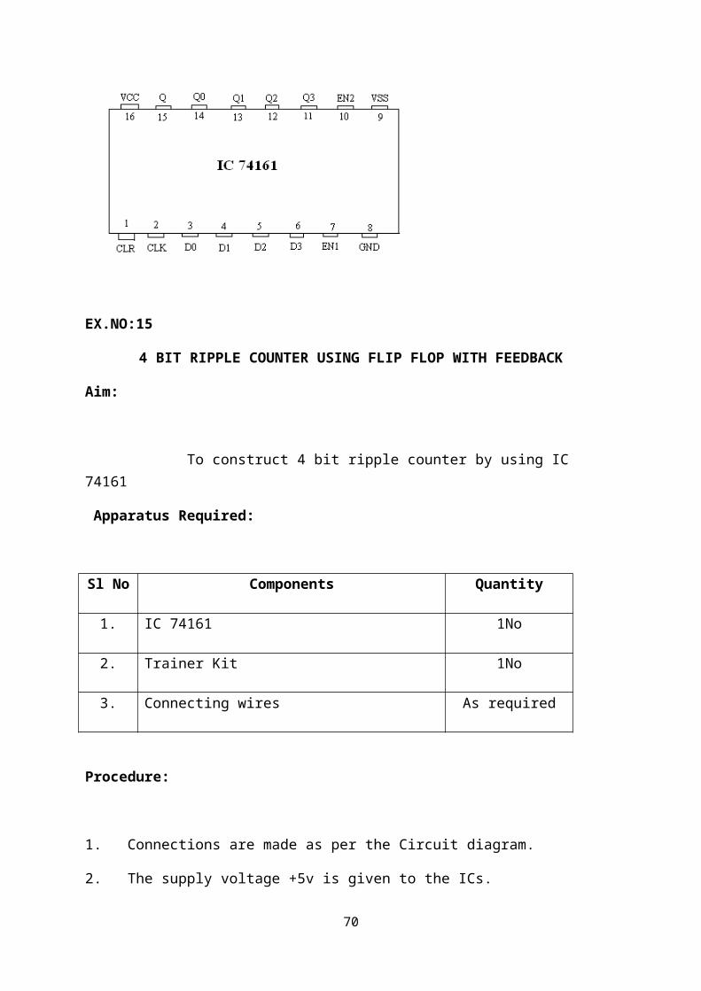
1 7 9 10 16
IC 14
2 74161 13
12
8 11

EX.NO:15
4 BIT RIPPLE COUNTER USING FLIP FLOP WITH FEEDBACK
Aim:
To construct 4 bit ripple counter by using IC 74161
Apparatus Required:
Sl No Components Quantity
1. IC 74161 1No
2. Trainer Kit 1No
3. Connecting wires As required
Procedure:
1. Connections are made as per the Circuit diagram.
2. The supply voltage +5v is given to the ICs.
3. Clock pulse is applied to the proper pin of the IC.
4. Outputs for different input conditions are verified as shown in the truth table.
59
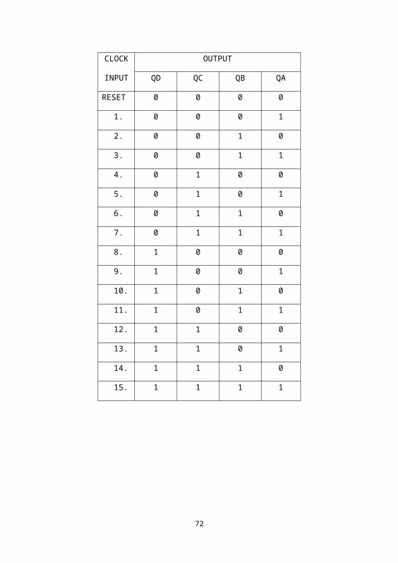
TABULATION:
60
CLOCK
INPUT
OUTPUT
QD QC QB QA
RESET 0 0 0 0
1. 0 0 0 1
2. 0 0 1 0
3. 0 0 1 1
4. 0 1 0 0
5. 0 1 0 1
6. 0 1 1 0
7. 0 1 1 1
8. 1 0 0 0
9. 1 0 0 1
10. 1 0 1 0
11. 1 0 1 1
12. 1 1 0 0
13. 1 1 0 1
14. 1 1 1 0
15. 1 1 1 1
Result:
Thus the 4 bit ripple counter is constructed by using IC 74161 and the corresponding truth tables are verified.
61

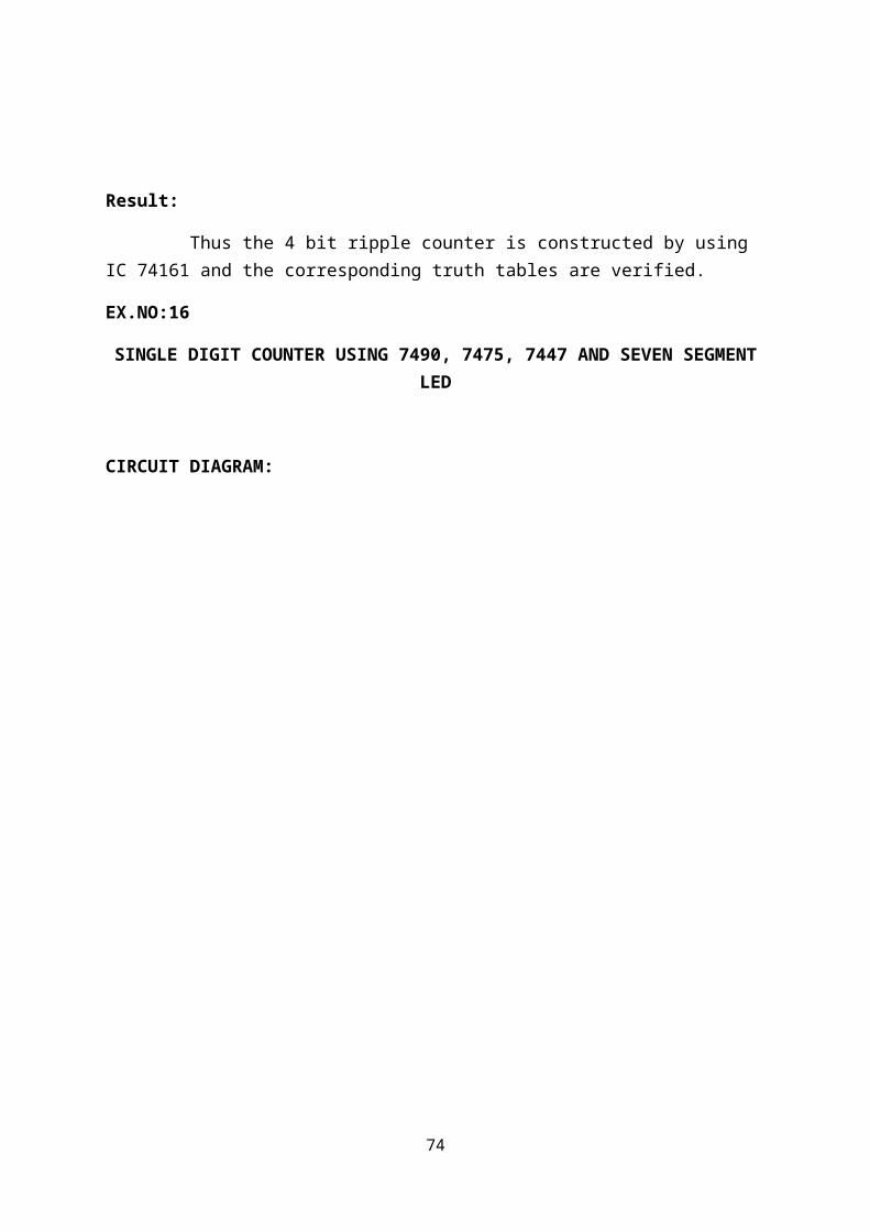
EX.NO:16
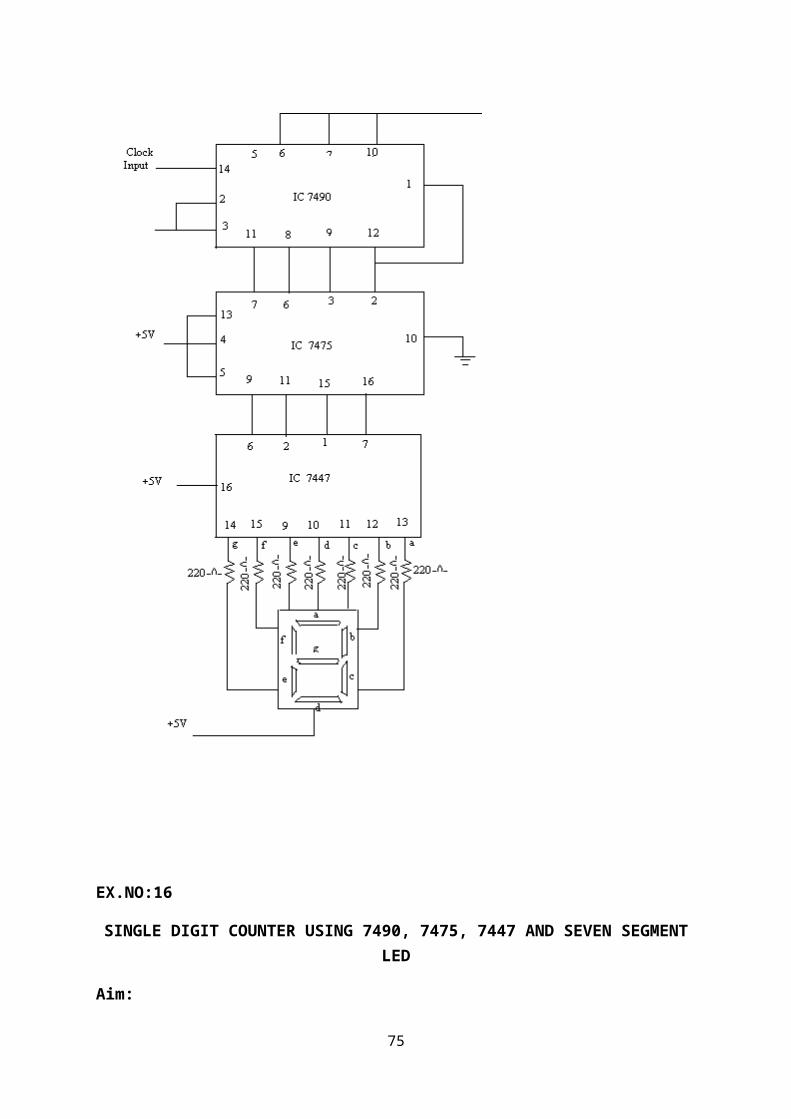
SINGLE DIGIT COUNTER USING 7490, 7475, 7447 AND SEVEN SEGMENT LED
CIRCUIT DIAGRAM:
62
EX.NO:16
SINGLE DIGIT COUNTER USING 7490, 7475, 7447 AND SEVEN SEGMENT LED
Aim:
To construct and test the performance of one digit counter using7490, 7495and 7447 seven segment LED display.
Apparatus Required:
Sl No Components Range Quantity
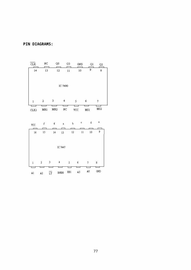
1. Decade counter 7490 1
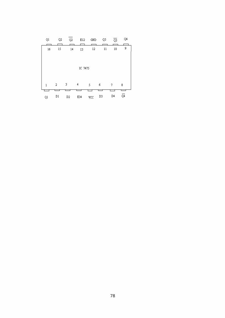
2. Latch circuit 7475 1
3. BCD to seven segment Decoder 7447 1
4. Seven segment LED display Common anode type 1
5. IC trainer board Digital 1
THEORY:
One digit counter is a counter, which will count the values from 0 to 9. We need IC 7490, 7475, 7447 and seven segment LED display for counting ( constructing ) one digit counter. The decade counter will count the binary values from 0000 to 1001. After that it will reset at the 10th clock pulse. The latch circuit connected in between counter and display section is used for controlling the signal flow. The IC 7447 converts the BCD code to its equivalent seven segment pattern for displaying the digit in a seven segment display unit.
Procedure:
1. Connections are made as per the Circuit diagram.
2. The supply voltage +5v is given to the ICs.
3. Clock pulse is applied to the proper pin of the IC.
4. Outputs for different input conditions are verified as shown in the truth table.
63

PIN DIAGRAMS:
64
65
Clock Input Digital Output
Reset
1
2
3
4
5
6
7
8
9
66
Result:
Thus the digital data generator using parallel to serial shift register IC 74165 receiving the serial data to parallel output using IC 74164 are verified
EX.NO:17
67

CONSTRUCT & TEST DIGITAL DATA GENERATOR USING PARALLEL TO SERIAL SHIFT REGISTER
CIRCUIT DIAGRAM
EX.NO:17
68
CONSTRUCT & TEST DIGITAL DATA GENERATOR USING PARALLEL TO SERIAL SHIFT REGISTER
Aim:
To construct and test the digital data generator using parallel to serial shift register IC 74165 receiving the serial data to parallel output using IC 74164
Apparatus Required:
Sl No Components Quantity
1. IC74194 1No
2. Trainer kit 1No
3. Multimeter 1No
4. Connecting wire 1No
Theory:
In digital system data is generated at one point serially transmitted to other place for data processing data generated by some encoding device and decoding obtain their 8 bit or 16 bit data and stored in sound register. The stored data is serially transmitted from one place to another place because of the economical reason. Since transmission of parallel data is proved to be costlier for this purpose shift register are used for carrying out the above job. In this experiment data is generated by operating 8 input switches. Data from the input switches given as input to a parallel in serial shift register 74165. The ic receives the parallel input data and stores it in a register inside it.
By suitable application of clock in other signals the data stored in a 74165 is shifted serially to another 74164. Where it is against stored in a register inside a IC the data such stored can be verified by the glowing LEDS connected to the output of 74164.
69
PROCEDURE:
70

For right shift
1. Connect mode control line to logic 0 and apply serial data at serial input terminal starting from LSB.
2. Apply clock pulse at clock1 terminal after each data bit observe output QA QB QC QD
3. Verify operations as right shift register (data shifted from QA to QB).
For left shift
1. Connect mode control line to logic 1 and apply serial data at D input starting from LSB
2. Connect QD to C, QC to B, QB to A
3. Apply clock pulse at clock2 ( pin8 )
4. Observe output QA QB QC QD and verify its operation as left shift register
Result:
Thus the digital data generator using parallel to serial shift register using IC 74194 are verified.
71
EX.NO:18
DAC USING R-2R NETWORK, BINARY WEIGHTED REGISTER NETWORK
CIRCUIT DIAGRAM:
TABULATION:
Digital Input Analog Output
-Vo VoltsC B A
72

EX.NO:18
DAC USING R-2R NETWORK, BINARY WEIGHTED REGISTER NETWORK
Aim:
To construct and test the performance of 3 digit binary weighted resistor digital to analog converted.
Apparatus Required:
Sl No Components Range Quantity
1. Op-amp IC 741 1No
2. Resister 1k,2k,4k 1No
3. Linear IC power supply 15V 1No
4. Regulated power supply (0-30)V 1No
5. Voltmeter (0-15)V 1No
6. Digital controlled switch 2-way switch 3Nos
Theory:
The digital to analog converter converts the applied input are in input terminal which are digital signal to its equivalent analog signal the applied input are in binary form.
The A,B,C are binary inputs, which are assumed to have values of 0or 1V. The operational amplifier act as a summing amplifier. The summing amplifier multiplies each input voltage by the ratio of feedback resister to its corresponding input resister the output voltage
Vo = -Rf\R * V\ 23-1 [23-1b3-1+23-2b3-2+23-3b3-3
= -Rf\R * V\ 22 [22b2+21b1+20b0]
Choose the value = R L V= 4V(22)
Vo= - [22b2+21b1+20b0]
= - [4c+2b+1a]
Where A,B&C are switch positions.
(2k & 4k resistors are formed by connecting two & four 1k resistor serially)
WEIGHTED REGISTER NETWORK
73
TABULATION:
Digital Input Analog Output
-Vo VoltsC B A
Procedure:
74
1. Connections are made as per the Circuit diagram.
2. The supply voltage +5v is given to the ICs.
3. Clock pulse is applied to the proper pin of the IC.
4. Outputs for different input conditions are verified as shown in the truth table.
Result:
Thus the 3 bit binary weighted resister D\A converter is constructed and its performance was tested.
75
EX.NO:19ADC USING IC ADC 0808
CIRCUIT DIAGRAM:
76
EX.NO:19
A/D CONVERTER USING ADC0808 ICAIM:
To verify the analog to digital conversion using ADC 0808 by study.
THEORY:
The A/D conversion is a quantizing process an analog signal is converted in to equivalent binary word. Thus the A/D converter is exactly opposite function that of the D/A converted.
ADC are classified broadly in to two groups according to their conversion technique direct type ADCs are integrating type ADCs direct type ADCs compare a given analog signal with the internally generated equivalent signal this groups includes
1. Flash type converter2. Counter type converter 3. Tracking or servo converter4. Successive approximation type converterIntegrating type ADCs performs conversion in a indirect manner by first changing the
analog input signal to the linear function of time or frequency. And then to a digital code. The two most widely used integrating types converters are
1. Charge balancing ADC 2. Dual slope ADC The most commonly used ADCs are successive approximation and the integrated type
the successive approximation ADCs are used in applications such as data loggers and instrumentation. Where conversion speed is important successive approximation and comparator type are faster but generally less accurate then integrating type convertors. the flash type is expensive for higher degree of accuracy. The integrating type convertor is used in applications such as digital meter, band meter and monitoring systems where the conversion accuracy is critical.
RESULT: Thus the analog to digital conversion using ADC 0808 is studied.
EX.NO:20
77
DAC USING IC DAC 0808
Digital OutputAnalog Output Volts
D7 D6 D5 D4 D3 D2 D1 D0
0 0 0 0 0 0 0 0 0V0 0 0 0 1 1 1 1 -1 1 1 1 1 1 0 0 -1 1 1 1 0 0 0 0 -1 1 1 1 1 1 0 0 -1 1 1 1 1 1 1 1 -
EX.NO:20
78

DAC USING IC DAC 0808 Aim:
To verify the operation DAC using IC DAC 0808
Apparatus Requied:
Sl.no Name of the Apparatus Range Quantity1. IC trainer kit - 1no2. Resistances 4 1no3. Voltmeter 0 to 15v
0 to 5v2no
4. DAC - 1no5. 7411C - 1no6. Multimeter - 1no
Theory:
The DAC is a digital to analog Voltage encoder. Digital signals are applied at the input of DAC and analog voltage is obtained as output. DAC is designated by the no. of inputs given to DAC. In this experiment 8 digit inputs are connected in to analog signal. Therefore it is called as 8 bit DAC. The IC no. is DAC0808.
Procedure:
1. The connection as per the circuit diagram.2. Power supply is connected to the circuit.3. The digital inputs are switched to DAC 0808 inputs in, sequential steps from
00000000 to 11111111 as shown in the tabular column.4. The corresponding obtained analog voltage is obtained as output.5. The reading are noted and tabulated.
Result:
Thus the operation DAC using IC DAC 0808 is constructed and tested.
79