ECE 5745 ASIC Tutorial - Cornell Universitycharacterize area and timing. 4. We use Synopsys...
14
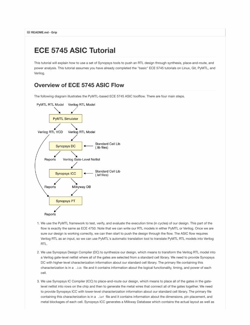
README.md - Grip ECE 5745 ASIC Tutorial This tutorial will explain how to use a set of Synopsys tools to push an RTL design through synthesis, place-and-route, and power analysis. This tutorial assumes you have already completed the "basic" ECE 5745 tutorials on Linux, Git, PyMTL, and Verilog. Overview of ECE 5745 ASIC Flow The following diagram illustrates the PyMTL-based ECE 5745 ASIC toolflow. There are four main steps. 1. We use the PyMTL framework to test, verify, and evaluate the execution time (in cycles) of our design. This part of the flow is exactly the same as ECE 4750. Note that we can write our RTL models in either PyMTL or Verilog. Once we are sure our design is working correctly, we can then start to push the design through the flow. The ASIC flow requires Verilog RTL as an input, so we can use PyMTL's automatic translation tool to translate PyMTL RTL models into Verilog RTL. 2. We use Synopsys Design Compiler (DC) to synthesize our design, which means to transform the Verilog RTL model into a Verilog gate-level netlist where all of the gates are selected from a standard cell library. We need to provide Synopsys DC with higher-level characterization information about our standard cell library. The primary file containing this characterization is in a .lib file and it contains information about the logical functionality, timing, and power of each cell. 3. We use Synopsys IC Compiler (ICC) to place-and-route our design, which means to place all of the gates in the gate- level netlist into rows on the chip and then to generate the metal wires that connect all of the gates together. We need to provide Synopsys ICC with lower-level characterization information about our standard cell library. The primary file containing this characterization is in a .lef file and it contains information about the dimensions, pin placement, and metal blockages of each cell. Synopsys ICC generates a Milkway Database which contains the actual layout as well as
Transcript of ECE 5745 ASIC Tutorial - Cornell Universitycharacterize area and timing. 4. We use Synopsys...
README.md - Grip
ECE 5745 ASIC TutorialThis tutorial will explain how to use a set of Synopsys tools to push an RTL design through synthesis, place-and-route, and
power analysis. This tutorial assumes you have already completed the "basic" ECE 5745 tutorials on Linux, Git, PyMTL, and
Verilog.
Overview of ECE 5745 ASIC Flow
The following diagram illustrates the PyMTL-based ECE 5745 ASIC toolflow. There are four main steps.
1. We use the PyMTL framework to test, verify, and evaluate the execution time (in cycles) of our design. This part of the
flow is exactly the same as ECE 4750. Note that we can write our RTL models in either PyMTL or Verilog. Once we are
sure our design is working correctly, we can then start to push the design through the flow. The ASIC flow requires
Verilog RTL as an input, so we can use PyMTL's automatic translation tool to translate PyMTL RTL models into Verilog
RTL.
2. We use Synopsys Design Compiler (DC) to synthesize our design, which means to transform the Verilog RTL model into
a Verilog gate-level netlist where all of the gates are selected from a standard cell library. We need to provide Synopsys
DC with higher-level characterization information about our standard cell library. The primary file containing this
characterization is in a .lib file and it contains information about the logical functionality, timing, and power of each
cell.
3. We use Synopsys IC Compiler (ICC) to place-and-route our design, which means to place all of the gates in the gate-
level netlist into rows on the chip and then to generate the metal wires that connect all of the gates together. We need
to provide Synopsys ICC with lower-level characterization information about our standard cell library. The primary file
containing this characterization is in a .lef file and it contains information about the dimensions, pin placement, and
metal blockages of each cell. Synopsys ICC generates a Milkway Database which contains the actual layout as well as

additional characterization information. Synopsys ICC also generates reports that can be used to more accurately
characterize area and timing.
4. We use Synopsys PrimeTime (PT) to perform power-analysis of our design. This requires switching activity information
for every net in the design (which comes from our Verilog RTL VCD file) and capacitance information for every net in the
design (which comes from the Milkyway Database generated by Synopsys ICC). Synopsys PT puts the switching
activity, capacitance, clock frequency, and voltage together to estimate the power consumption of every net and thus
every module in the design.
Extensive documentation is provided by Synopsys for Design Compiler, IC Compiler, and PrimeTime. We have organized
this documentation and made it available to you on the public course webpage. The username/password was distributed
during lecture.
PyMTL-Based Testing, Simulation, TranslationFirst step is to source the setup script and clone the tutorial repository from GitHub. We create a bash variable to keep track
of the tutorial directory.
% source setup-‐ece5745.sh % mkdir $HOME/ece5745 % cd $HOME/ece5745 % git clone [email protected]:cornell-‐ece5745/ece5745-‐tut-‐asic % cd ece5745-‐tut-‐asic % TOPDIR=$PWD
We will be pushing the sort unit from the PyMTL tutorial through the ASIC flow. As a reminder, the sort unit takes as input
four integers and a valid bit and outputs those same four integers in increasing order with the valid bit. The sort unit is
implemented using a three-stage pipelined, bitonic sorting network and the datapath is shown below.
Run the tests for the sort unit and note that the tests for the SortUnitStructRTL will fail. You can just copy over your
implementation of the MinMaxUnit from when you completed the PyMTL tutorial. If you have not completed the PyMTL
tutorial then go back and do that now. After running the tests we use the sort unit simulator to translate the PyMTL RTL
model into Verilog and to dump the VCD file that we want to use for power analysis.
% mkdir $TOPDIR/pymtl/build % cd $TOPDIR/pymtl/build % py.test ../tut3_pymtl/sort % ../tut3_pymtl/sort/sort-‐sim -‐-‐impl rtl-‐struct -‐-‐translate -‐-‐dump-‐vcd
Take a moment to open up the translated Verilog which should be in a file named SortUnitStructRTL_0x73ab8da9cdd886de.v .
The complicated hash suffix is used by PyMTL to make this filename unique even for parameterized modules which are
instantiated for a specific set of parameters. The hash might be different for your design. Try to see how both the structural
composition and the behavioral modeling translates into Verilog. Here is an example of the translation for the MinMaxUnit .
Notice how PyMTL will output the source Python embedded as a comment in the corresponding translated Verilog.
module MinMaxUnit_0x152ab97dfd22b898 ( input wire [ 0:0] clk, input wire [ 7:0] in0, input wire [ 7:0] in1,

output reg [ 7:0] out_max,
output reg [ 7:0] out_min,
input wire [ 0:0] reset
);
// PYMTL SOURCE:
//
// @s.combinational
// def block():
//
// if s.in0 >= s.in1:
// s.out_max.value = s.in0
// s.out_min.value = s.in1
// else:
// s.out_max.value = s.in1
// s.out_min.value = s.in0
// logic for block()
always @ (*) begin
if ((in0 >= in1)) begin
out_max = in0;
out_min = in1;
end
else begin
out_max = in1;
out_min = in0;
end
end
endmodule // MinMaxUnit_0x4b8e51bd8055176a
Although we hope students will not need to actually open up this translated Verilog it is occasionally necessary. For
example, PyMTL is not perfect and can translate incorrectly which might require looking at the Verilog to see where it went
wrong. Other steps in the ASIC flow might refer to an error in the translated Verilog which will also require looking at the
Verilog to figure out why the other steps are going wrong. While we try and make things as automated as possible, students
will eventually need to dig in and debug some of these steps themselves.
Using Synopsys Design Compiler ManuallyWe use Synopsys Design Compiler (DC) to synthesize Verilog RTL models into a gate-level netlist where all of the gates are
from the standard cell library. So Synopsys DC will synthesize the Verilog + operator into a specific arithmetic block at the
gate-level. Based on various constraints it may synthesize a ripple-carry adder, a carry-look-ahead adder, or even more
advanced parallel-prefix adders.
We will start by manually entering a sequence of commands into Synopsys DC and in the next section we will see how to
automate this process. Create a directory to work in and launch Synopsys DC.
% mkdir $TOPDIR/asic/dc-‐syn/manual-‐dc
% cd $TOPDIR/asic/dc-‐syn/manual-‐dc
% dc_shell-‐xg-‐t
To make it easier to copy-and-paste commands from this document, we tell Synopsys DC to ignore the prefix dc_shell>
using the following:
dc_shell> alias "dc_shell>" ""
Before we can really start synthesizing the design we need to setup a bunch of variables and options. We need to point
Synopsys DC to where the standard cells are installed, where the Verilog we want to synthesize is located, where the
standard cell characterization files are located, and what the names for logic 0 and logic 1 are in the standard cell library.
dc_shell> set stdcells_home /classes/ece5745/install/bare-‐pkgs/noarch/saed-‐90nm-‐synopsys-‐cells
dc_shell> set_app_var search_path "$stdcells_home ../../../pymtl/build"
dc_shell> set_app_var target_library "cells.db"

dc_shell> set_app_var link_library "* $target_library"
dc_shell> set_app_var alib_library_analysis_path \
"/classes/ece5745/install/bare-‐pkgs/noarch/saed-‐90nm-‐synopsys-‐cells"
dc_shell> set_app_var mw_logic1_net "VDD"
dc_shell> set_app_var mw_logic0_net "VSS"
Now we create a new Milkyway Database. Milkyway is Synopsys' proprietary database format which is used to hold all
kinds of design data (RTL models, gate-level models, standard-cell models, timing information, layout, etc). We open the
new database and also create a directory for Synopsys DC to work in.
dc_shell> create_mw_lib -‐technology $stdcells_home/cells.tf \
-‐mw_reference_library $stdcells_home/cells.fr "LIB"
dc_shell> open_mw_lib "LIB"
dc_shell> define_design_lib WORK -‐path "./work"
We are now ready to synthesize the design. We first read in the Verilog file which contains the top-level design and all
referenced modules.
dc_shell> analyze -‐format verilog "SortUnitStructRTL_0x73ab8da9cdd886de.v"
We use the elaborate command to convert the Verilog models into a unified in-memory model format that Synopsys can
analyze. This is also when Synopsys starts to do some analysis on the design, and the command output can sometimes
display useful information about inferred latches and such. Notice that you need to give the elaborate command the name
of the Verilog module which is the top of the design.
dc_shell> elaborate "SortUnitStructRTL_0x73ab8da9cdd886de"
We use the link command to resolve all module references and then we use the check_design command to check for any
warnings or errors. Always be sure to explicitly look for errors; they can get buried in the tons of output that the Synopsys
tools produce. Synopsys DC does not usually stop if there is an error but instead just keeps going.
dc_shell> link
dc_shell> check_design
We need to create a clock constraint to tell Synopsys DC what our target cycle time is. Synopsys DC will not synthesize a
design to run "as fast as possible". Instead, the designer gives Synopsys DC a target cycle time and the tool will try to meet
this constraint while minimizing area and power. The create_clock command takes the name of the clock signal in the
Verilog (which in this course will always be clk ), the label to give this clock (i.e., ideal_clock1 ), and the target clock period
in nanoseconds. So in this example, we are asking Synopsys DC to see if it can synthesize the design to run at 1GHz (i.e., a
cycle time of 1ns).
dc_shell> create_clock clk -‐name ideal_clock1 -‐period 1
Finally, the compile_ultra command will do the synthesis. Without any options, the compile_ultra command will
sometimes flatten parts of the design. Flatten means to remove module hierarchy boundaries; so instead of having module
A and module B within module C, Synopsys DC will take all of the logic in module A and module B and put it directly in
module C. Without these extra hierarchy boundaries, Synopsys DC is able to perform more optimizations and potentially
achieve better area, energy, and timing. The -‐no_autoungroup option prevents Synopsys DC from flattening any part of the
design and thus preserves the module hierarchy. This makes it much easier to interpret the reports since if there is a module
A in your RTL design that same module will always be in the synthesized gate-level netlist.
dc_shell> compile_ultra -‐no_autoungroup
As compile_ultra runs it will display how it is trying to optimize your design. Synopsys DC will use sophisticated CAD
algorithms to try and meet the clock cycle constraint, then to reduce the area/power overhead, and then to again improve

the timing. It will iterate many times as it works hard to optimize the design.
Now that we have synthesized the design, we output the resulting gate-level netlist in two different file formats: Verilog and
DDC (which we will use with DesignVision).
dc_shell> write -‐f verilog -‐hierarchy -‐output SortUnitStructRTL_0x73ab8da9cdd886de.mapped.v
dc_shell> write -‐format ddc -‐hierarchy -‐output SortUnitStructRTL_0x73ab8da9cdd886de.mapped.ddc
We can use various commands to generate reports about area, energy, and timing. The report_timing command will show
the critical path through the design. Part of the report is displayed below.
dc_shell> report_timing -‐transition_time -‐nets -‐attributes -‐nosplit
...
Point Fanout Trans Incr Path
-‐-‐-‐-‐-‐-‐-‐-‐-‐-‐-‐-‐-‐-‐-‐-‐-‐-‐-‐-‐-‐-‐-‐-‐-‐-‐-‐-‐-‐-‐-‐-‐-‐-‐-‐-‐-‐-‐-‐-‐-‐-‐-‐-‐-‐-‐-‐-‐-‐-‐-‐-‐-‐-‐-‐-‐-‐-‐-‐-‐-‐-‐-‐-‐-‐-‐-‐-‐-‐-‐-‐-‐-‐-‐
clock network delay (ideal) 0.00 0.00
elm_S1S2$001/out_reg[1]/CLK (DFFARX1) 0.00 0.00 0.00 r
elm_S1S2$001/out_reg[1]/Q (DFFARX1) 0.04 0.18 0.18 r
elm_S1S2$001/out[1] (net) 2 0.00 0.18 r
elm_S1S2$001/out[1] (Reg_0x45f1552f10c5f05d_10) 0.00 0.18 r
elm_S1S2$001$out[1] (net) 0.00 0.18 r
minmax1_S2/in0[1] (MinMaxUnit_0x152ab97dfd22b898_1) 0.00 0.18 r
minmax1_S2/in0[1] (net) 0.00 0.18 r
minmax1_S2/U28/ZN (INVX0) 0.04 0.09 0.26 f
minmax1_S2/n32 (net) 2 0.00 0.26 f
minmax1_S2/U31/Q (OA22X1) 0.03 0.13 0.40 f
minmax1_S2/n15 (net) 1 0.00 0.40 f
minmax1_S2/U32/Q (OA22X1) 0.03 0.11 0.50 f
minmax1_S2/n18 (net) 1 0.00 0.50 f
minmax1_S2/U33/Q (OA22X1) 0.03 0.11 0.61 f
minmax1_S2/n21 (net) 1 0.00 0.61 f
minmax1_S2/U34/Q (OA22X1) 0.03 0.11 0.72 f
minmax1_S2/n24 (net) 1 0.00 0.72 f
minmax1_S2/U35/Q (OA22X1) 0.04 0.11 0.83 f
minmax1_S2/n27 (net) 2 0.00 0.83 f
minmax1_S2/U4/Q (OA22X1) 0.05 0.13 0.96 f
minmax1_S2/n2 (net) 4 0.00 0.96 f
minmax1_S2/U6/Q (OA22X1) 0.05 0.14 1.10 f
minmax1_S2/n4 (net) 2 0.00 1.10 f
minmax1_S2/U40/Q (MUX21X1) 0.03 0.17 1.27 r
minmax1_S2/out_max[0] (net) 1 0.00 1.27 r
minmax1_S2/out_max[0] (MinMaxUnit_0x152ab97dfd22b898_1) 0.00 1.27 r
minmax1_S2$out_max[0] (net) 0.00 1.27 r
elm_S2S3$003/in_[0] (Reg_0x45f1552f10c5f05d_0) 0.00 1.27 r
elm_S2S3$003/in_[0] (net) 0.00 1.27 r
elm_S2S3$003/out_reg[0]/D (DFFX2) 0.03 0.04 1.31 r
data arrival time 1.31
clock ideal_clock1 (rise edge) 1.00 1.00
clock network delay (ideal) 0.00 1.00
elm_S2S3$003/out_reg[0]/CLK (DFFX2) 0.00 1.00 r
library setup time -‐0.08 0.92
data required time 0.92
-‐-‐-‐-‐-‐-‐-‐-‐-‐-‐-‐-‐-‐-‐-‐-‐-‐-‐-‐-‐-‐-‐-‐-‐-‐-‐-‐-‐-‐-‐-‐-‐-‐-‐-‐-‐-‐-‐-‐-‐-‐-‐-‐-‐-‐-‐-‐-‐-‐-‐-‐-‐-‐-‐-‐-‐-‐-‐-‐-‐-‐-‐-‐-‐-‐-‐-‐-‐-‐-‐-‐-‐-‐-‐
data required time 0.92
data arrival time -‐1.31
-‐-‐-‐-‐-‐-‐-‐-‐-‐-‐-‐-‐-‐-‐-‐-‐-‐-‐-‐-‐-‐-‐-‐-‐-‐-‐-‐-‐-‐-‐-‐-‐-‐-‐-‐-‐-‐-‐-‐-‐-‐-‐-‐-‐-‐-‐-‐-‐-‐-‐-‐-‐-‐-‐-‐-‐-‐-‐-‐-‐-‐-‐-‐-‐-‐-‐-‐-‐-‐-‐-‐-‐-‐-‐
slack (VIOLATED) -‐0.39
This timing report uses static timing analysis to find the critical path. Static timing analysis checks the timing across all paths
in the design (regardless of whether these paths can actually be used in practice) and finds the longest path. You can learn
more about static timing analysis in Chapter 1 of the Synopsys Timing Constraints and Optimization User Guide. The report
clearly shows that the critical path starts at the first pipeline register in between the S1 and S2 stages, goes into the first
input of the bottom MinMaxUnit , comes out the out_min port of the MinMaxUnit , and ends at a pipeline register in between
the S2 and S3 stages. The report shows the delay through each logic gate (e.g., the clk-to-q delay of the initial DFF is
180ps, the propagation delay of a OA22X1 gate is 130ps) and the total delay for the critical path which in this case is
1.31ns. Notice how the OA22X1 gates do not all have the same propagation delay; this is because the static timing analysis
also factors in input slew rates, rise vs fall time, and output load when calculating the delay of each gate. We set the clock

constraint to be 1ns, but also notice that the report factors in the setup time required at the final register. The setup time is80ps, so in order to operate the sort unit at 1ns and meet the setup time we would need the critical path to arrive in 0.92ns.
The difference between the required arrival time and the actual arrival time is called the slack. Positive slack means the patharrived before it needed to while negative slack means the path arrived after it needed to. If you end up with positive slack itmeans you probably want to decrease your clock constraint to push the tools harder and produce a faster design. Even ifyou have no slack you still probably want to decrease your clock constraint. This is because the tools rarely leave positiveslack preferring instead to take an overly fast design and resynthesize smaller logic to save area and power. In the aboveexample, we have 390ps of negative slack. Note that this does not mean the sort unit will not work. It just means the cycletime would have to be 1.39ns in order for the sort unit to operate correctly. Because in this course we are primarilyinterested in design-space exploration (as opposed to meeting some kind of arbitrary timing constraint), we suggestadjusting the clock constraint until you end up with about 5-10% negative slack. This will result in a well-optimized designand help identify the "fundamental" performance of the design.
The report_area command can show how much area each module uses and can enable detailed area breakdown analysis.
dc_shell> report_area -‐nosplit -‐hierarchy
...
Global Local
Cell Area Cell Area
-‐-‐-‐-‐-‐-‐-‐-‐-‐-‐ -‐-‐-‐-‐-‐-‐-‐-‐-‐-‐-‐-‐-‐-‐-‐-‐
Hierarchical cell Abs Non Black-‐
Total % Comb Comb boxes
-‐-‐-‐-‐-‐-‐-‐-‐-‐-‐-‐-‐-‐-‐-‐-‐-‐-‐ -‐-‐-‐-‐-‐ -‐-‐-‐ -‐-‐-‐-‐-‐ -‐-‐-‐-‐-‐ -‐-‐-‐ -‐-‐-‐-‐-‐-‐-‐-‐-‐-‐-‐-‐-‐-‐-‐-‐-‐-‐-‐-‐-‐-‐-‐-‐-‐-‐-‐-‐-‐-‐-‐
SortUnitStructRTL
elm_S0S1$000 199.0 4.1 0.0 199.0 0.0 Reg_0x45f1552f10c5f05d_7
elm_S0S1$001 199.0 4.1 0.0 199.0 0.0 Reg_0x45f1552f10c5f05d_6
elm_S0S1$002 199.0 4.1 0.0 199.0 0.0 Reg_0x45f1552f10c5f05d_5
elm_S0S1$003 199.0 4.1 0.0 199.0 0.0 Reg_0x45f1552f10c5f05d_4
elm_S1S2$000 233.1 4.8 0.0 233.1 0.0 Reg_0x45f1552f10c5f05d_11
elm_S1S2$001 250.6 5.1 0.0 250.6 0.0 Reg_0x45f1552f10c5f05d_10
elm_S1S2$002 237.7 4.9 0.0 237.7 0.0 Reg_0x45f1552f10c5f05d_9
elm_S1S2$003 231.3 4.7 0.0 231.3 0.0 Reg_0x45f1552f10c5f05d_8
elm_S2S3$000 244.2 5.0 0.0 244.2 0.0 Reg_0x45f1552f10c5f05d_3
elm_S2S3$001 244.2 5.0 0.0 244.2 0.0 Reg_0x45f1552f10c5f05d_2
elm_S2S3$002 231.3 4.7 0.0 231.3 0.0 Reg_0x45f1552f10c5f05d_1
elm_S2S3$003 245.1 5.0 0.0 245.1 0.0 Reg_0x45f1552f10c5f05d_0
minmax0_S1 431.3 8.8 431.3 0.0 0.0 MinMaxUnit_0x152ab97dfd22b898_2
minmax0_S2 460.8 9.4 460.8 0.0 0.0 MinMaxUnit_0x152ab97dfd22b898_3
minmax1_S1 447.8 9.1 447.8 0.0 0.0 MinMaxUnit_0x152ab97dfd22b898_4
minmax1_S2 437.7 8.9 437.7 0.0 0.0 MinMaxUnit_0x152ab97dfd22b898_1
minmax_S3 313.3 6.4 313.3 0.0 0.0 MinMaxUnit_0x152ab97dfd22b898_0
val_S0S1 35.9 0.7 11.0 24.8 0.0 RegRst_0x2ce052f8c32c5c39_0
val_S1S2 30.4 0.6 5.5 24.8 0.0 RegRst_0x2ce052f8c32c5c39_1
val_S2S3 30.4 0.6 5.5 24.8 0.0 RegRst_0x2ce052f8c32c5c39_2
-‐-‐-‐-‐-‐-‐-‐-‐-‐-‐-‐-‐-‐-‐-‐-‐-‐-‐ -‐-‐-‐-‐-‐-‐ -‐-‐-‐ -‐-‐-‐-‐-‐-‐ -‐-‐-‐-‐-‐-‐ -‐-‐-‐ -‐-‐-‐-‐-‐-‐-‐-‐-‐-‐-‐-‐-‐-‐-‐-‐-‐-‐-‐-‐-‐-‐-‐-‐-‐-‐-‐-‐-‐-‐-‐
Total 2113.2 2788.7 0.0
The units are in square micron. From the above report, we can see that each pipeline register consumes about 4-5% of thearea, while the MinMaxUnits consume a total of 43% of the area. This is one reason we try not to flatten our designs, sincethe module hierarchy helps us understand the area breakdowns. If we completely flattened the design there would only beone line in the above table.
The report_power command can show how much power each module consumes. Note that this power analysis is actuallynot that useful yet, since at this stage of the flow the power analysis is based purely on statistical activity factor estimation.Basically, Synopsys DC assumes every net toggles 10% of the time. This is a pretty poor estimate.
dc_shell> report_power -‐nosplit -‐hier
Finally, we go ahead and exit Synopsys DC.
dc_shell> exit
Take a few minutes to examine the resulting Verilog gate-level netlist. Notice that the module hierarchy is preserved and also
notice that the MinMaxUnit synthesizes into a large number of basic logic gates.
% cd $TOPDIR/asic/dc-‐syn/manual-‐dc
% more SortUnitStructRTL_0x73ab8da9cdd886de.mapped.v
We can use the Synopsys Design Vision tool for browsing the resulting gate-level netlist, plotting critical path histograms,
and generally analyzing our design. Start Synopsys Design Vision and setup the various variables and options as follows:
% design_vision-‐xg
design_vision> alias "design_vision>" ""
design_vision> set stdcells_home /classes/ece5745/install/bare-‐pkgs/noarch/saed-‐90nm-‐synopsys-‐cells
design_vision> set_app_var search_path "$stdcells_home ../../../pymtl/build"
design_vision> set_app_var target_library "cells.db"
design_vision> set_app_var link_library "* $target_library"
design_vision> set_app_var alib_library_analysis_path \
"/classes/ece5745/install/bare-‐pkgs/noarch/saed-‐90nm-‐synopsys-‐cells/alib"
Now choose File > Read from the menu and open the SortUnitStructRTL_0x73ab8da9cdd886de.mapped.ddc file. To view a
schematic of the gate-level netlist, right click on the module in the module hierarchy browser and choose Schematic View.
Open the top-level module as a gate-level netlist and then double click on the box to see the MinMaxUnits . To see a
histogram of path slack choose Timing > Paths Slack from the menu, and the click OK. To see a schematic of the critical
path, first click on one of the bars in the path slack histogram, and then right click on a specific path from the list that will
appear to the right of the histogram. Choose Path Inspector.
Using Synopsys Design Compiler with MakefileObviously entering all of the above commands is tedious and error prone. We could also potentially directly drive synthesis
using the Design Vision GUI, but that is just as tedious and error prone. To enable an agile hardware design methodology,
we must script as much of the ASIC flow as possible. Luckily, Synopsys tools can be easily scripted using TCL, and even
better, the ECE 5745 staff have already created these TCL scripts. The ECE 5745 TCL scripts were based on the Synopsys
reference methodology which is copyrighted by Synopsys. This means you cannot take this repo and/or the scripts and
make them public. Please keep this in mind.
We use make to drive the ASIC flow. A special Makefrag describes the details of the specific design you want to push
through the flow. Go into the asic subdirectory and take a look at the Makefrag .
% cd $TOPDIR/asic
% more Makefrag
The Makefrag has one entry for each design. Each entry looks like this:
ifeq ($(design),pymtl-‐sort)
flow = pymtl
clock_period = 1.0
sim_build_dir = pymtl/build
vsrc = SortUnitStructRTL_0x73ab8da9cdd886de.v
vmname = SortUnitStructRTL_0x73ab8da9cdd886de
viname = TOP/v
vcd = sort-‐rtl-‐struct-‐random.verilator1.vcd
endif
Every design has a name and in this case the design name is pymtl-‐sort . For now the flow variable will always be pymtl ,
the sim_build_dir variable will always be pymtl/build , and the viname variable will always be TOP/v . The clock_period
variable is where you set the target clock period constraint for this design. The vsrc variable is the name of the Verilog file
you want to push through the flow. The vmname variable is the name of the Verilog module which is the top of the design.
For now it will always be the Verilog file name without the .v suffix. Finally, the vcd variable is the name of the VCD file you
want to use for power analysis.
We set the following line in the Makefrag to choose which design we want to push through the flow:

design = pymtl-‐sort
Since this is already set to push our sort unit through the flow, we are all set. Now all we need to do use make like this:
% cd $TOPDIR/asic/dc-‐syn % make
You will see make run some commands, start Synopsys DC, run some TCL scripts, and then finish up. Essentially, theautomated system is doing something very similar to what we did in the previous section manually.
If Synopsys DC exits with a status code of zero then something went wrong. You will need to carefully look through the logto search for errors or warnings that might hint at what went wrong. You may have used the incorrect file/module names inthe Makefrag or there might be code in your Verilog RTL that is not synthesizable. This is not easy and there is no simpleway to figure out these issues. You just need to poke through the log file:
% cd $TOPDIR/asic/dc-‐syn/current-‐dc/log % more dc.log
When the synthesis is completed you can take a look at the resulting Verilog gate-level netlist here:
% cd $TOPDIR/asic/dc-‐syn/current-‐dc/results % more SortUnitStructRTL_0x73ab8da9cdd886de.mapped.v
The automated system is also setup to output a bunch of reports. Here are the key ones:
% cd $TOPDIR/asic/dc-‐syn/current-‐dc/reports % more SortUnitStructRTL_0x73ab8da9cdd886de.mapped.qor.rpt % more SortUnitStructRTL_0x73ab8da9cdd886de.mapped.timing.rpt % more SortUnitStructRTL_0x73ab8da9cdd886de.mapped.area.rpt % more SortUnitStructRTL_0x73ab8da9cdd886de.mapped.power.rpt
The quality-of-results (QOR) report is a particularly useful summary. If you take a look that report you will see something likethis:
Timing Path Group 'REGIN' -‐-‐-‐-‐-‐-‐-‐-‐-‐-‐-‐-‐-‐-‐-‐-‐-‐-‐-‐-‐-‐-‐-‐-‐-‐-‐-‐-‐-‐-‐-‐-‐-‐-‐-‐ Levels of Logic: 2.00 Critical Path Length: 0.06 Critical Path Slack: 0.87 Critical Path Clk Period: 1.00 Total Negative Slack: 0.00 No. of Violating Paths: 0.00 Worst Hold Violation: 0.00 Total Hold Violation: 0.00 No. of Hold Violations: 0.00 -‐-‐-‐-‐-‐-‐-‐-‐-‐-‐-‐-‐-‐-‐-‐-‐-‐-‐-‐-‐-‐-‐-‐-‐-‐-‐-‐-‐-‐-‐-‐-‐-‐-‐-‐
Timing Path Group 'REGOUT' -‐-‐-‐-‐-‐-‐-‐-‐-‐-‐-‐-‐-‐-‐-‐-‐-‐-‐-‐-‐-‐-‐-‐-‐-‐-‐-‐-‐-‐-‐-‐-‐-‐-‐-‐ Levels of Logic: 9.00 Critical Path Length: 0.85 Critical Path Slack: 0.15 Critical Path Clk Period: 1.00 Total Negative Slack: 0.00 No. of Violating Paths: 0.00 Worst Hold Violation: 0.00 Total Hold Violation: 0.00 No. of Hold Violations: 0.00 -‐-‐-‐-‐-‐-‐-‐-‐-‐-‐-‐-‐-‐-‐-‐-‐-‐-‐-‐-‐-‐-‐-‐-‐-‐-‐-‐-‐-‐-‐-‐-‐-‐-‐-‐
Timing Path Group 'ideal_clock1' -‐-‐-‐-‐-‐-‐-‐-‐-‐-‐-‐-‐-‐-‐-‐-‐-‐-‐-‐-‐-‐-‐-‐-‐-‐-‐-‐-‐-‐-‐-‐-‐-‐-‐-‐ Levels of Logic: 9.00 Critical Path Length: 0.88

Critical Path Slack: 0.05 Critical Path Clk Period: 1.00 Total Negative Slack: 0.00 No. of Violating Paths: 0.00 Worst Hold Violation: 0.00 Total Hold Violation: 0.00 No. of Hold Violations: 0.00 -‐-‐-‐-‐-‐-‐-‐-‐-‐-‐-‐-‐-‐-‐-‐-‐-‐-‐-‐-‐-‐-‐-‐-‐-‐-‐-‐-‐-‐-‐-‐-‐-‐-‐-‐
Paths are organized into four groups: REGIN, REGOUT, INOUT, and CLK path groups. REGIN paths start at an input portand end at a register; REGOUT paths start at a register and end at an output port; INOUT paths start at an input port andend at an output port; and CLK paths start at a register and end at register. The following diagram is from Chapter 1 of theSynopsys Timing Constraints and Optimization User Guide.
We have setup the flow so that the tools have to fit all four of these paths in a single cycle. The QOR report shows the worstpath within each path group. The overall critical path for your design will be the worse critical path across all four groups,and the actual cycle time is calculated as the "Critical Path Clk Period" (this is the target clock constraint) minus the "CriticalPath Slack"). So in this example the cycle time would be 0.95ns. Recall that when we manually entered the commands forsynthesis the critical path was 1.39ns. What changed? The automated flow takes advantage of what is known as"topological mode"; this is an advanced feature in Synopsys DC which involves more complex algorithms that do synthesis,preliminary placement, more synthesis, and more preliminary placement. By incorporating some preliminary placementalgorithms into the synthesis part of the flow, Synopsys DC is able to achieve much higher QOR.
Keep in mid that the area, energy, timing results post-synthesis will not be as accurate as the post-place-and-route results.While it is fine to iterate quickly just using synthesis, you will eventually need to use Synopsys IC Compiler for more accuratearea and timing analysis, and use Synopsys PrimeTime for more accurate power analysis.
Using IC Compiler with MakefileWe use Synopsys IC Compiler (ICC) for placing and routing standard cells, but also for power routing and clock treesynthesis. The Verilog gate-level netlist generated by Synopsys DC has no physical information: it is just a netlist, so theSynopsys IC will first try and do a rough placement of all of the gates into rows on the chip. Synopsys IC will then do somepreliminary routing, and iterate between more and more detailed placement and routing until it reaches the target cycle time(or gives up). Synopsys IC will also route all of the power and ground rails in a grid and connect this grid to the power andground pins of each standard cell, and Synopsys IC will automatically generate a clock tree to distribute the clock to allsequential state elements with hopefully low skew.
We can use make to run Synopsys ICC like this:
% cd $TOPDIR/asic/icc-‐par % make
Place-and-route can take significantly longer than synthesis, so be prepared to wait a while with larger designs. If you lookat the output scrolling by you will see some of the optimization passes as Synopsys ICC attempts to iteratively improve thedesign. The automated system is also setup to output a bunch of reports. Here are the key ones:

% cd $TOPDIR/asic/icc-‐par/current-‐icc/reports % more chip_finish_icc.qor.rpt % more chip_finish_icc.timing.rpt % more chip_finish_icc.area.rpt % more chip_finish_icc.power.rpt % more summary.txt
vsrc = SortUnitStructRTL_0x73ab8da9cdd886de.v area = 5072 # um^2 constraint = 1.0 # ns slack = 0.01 # ns cycle_time = 0.99 # ns
If Synopsys ICC exits with an error or the reports look very odd, you will need to carefully look through the log to search for
errors or warnings that might hint at what went wrong. Usually we catch errors in Synopsys DC and after that we are all set,
so you might want to go back and see if there were any errors in Synopsys DC. The Synopsys ICC log files are here:
% cd $TOPDIR/asic/dc-‐syn/current-‐iccdp/log % cd $TOPDIR/asic/dc-‐syn/current-‐icc/log
We have written a little script to parse the reports and generate a summary.txt file. This script takes care of looking across
all four path groups to fine the true cycle time that you should use in your analysis. The general format of the area, energy,
timing reports is similar in spirit to what we saw earlier when working with Synopsys DC.
From the summary.txt file, we can see that the cycle time is now estimated to be 0.99ns, but recall that our post-synthesis
estimate was 0.95ns. The key difference of course, is that these results are based on post-place-and-route analysis so they
factor in routing congestion and interconnect overheads.
While we do not use GUIs to drive our flow, we often use GUIs to analyze the results. You can start the Synopsys ICC GUI to
visualize the final layout like this:
% cd $TOPDIR/asic/icc-‐par/current-‐icc % icc_shell -‐gui
Once the GUI has finished loading you will viewing a "MainWindow", use the following steps to actually open up the most
recently placed-and-routed design in a "LayoutWindow":
enter source icc_setup.tcl at icc_shell> prompt
Chose File > Open Design... from the menu
Click the folder button to right of Library Name
Select the orange folder with L in file browser
Select chip_finish_icc in list
Click Okay
We call the resulting plot an "amoeba plot" because the tool often generates blocks that look like amoebas. You can now
zoom in to see how the standard cells were placed and how the routing was done. You can turn on an off the visibility of
metal layers using the panel on the left. One very useful feature is to view the hierarchy and area breakdown. This will be
critical for producing high-quality amoeba plots. You can use the following steps to highlight various modules on the
amoeba plot:
Choose Placement > Color By Hierarchy from the menu
In the sidebar menu on right, select Reload
In the pop-up window, select Color hierarchical cells at level
Click OK in the pop up
Click checkmark and apply to show just one component
Another very useful feature is to highlight the critical path on the amoeba plot using the following steps:
Choose Timing > New Timing Analysis Window from the menu
Focus on Select Paths window, click OK

List of paths should appear
Click on path to see it highlighted in the layout view
You can see an example amoeba plot below. Note that you will need to use some kind of "screen-capture" software to
capture the plot and by default it will have a black background. We strongly recommend inverting the colors so that the
amoeba plot you include in your reports is dark on white (instead of white on dark). This makes the chip plot easier to read.
You will also need to play with the colors to enable easily seeing the various parts of your design. In this example, we have
chosen to highlight the five MinMaxUnits (brown, blue, green, red, gray) and one of the critical paths which goes through the
red MinMaxUnit . Note how the tool has actually spread the red MinMaxUnit a part a bit. Keep in mind that these tools use
incredibly sophisticated heuristics and so it can sometimes be difficult to understand every detail about why it places cells
in specific places.
Using Primetime with MakefileWe use Synopsys PrimeTime (PT) for power analysis. There are many ways to perform power analysis. The power post-
synthesis and post-place-and-route power reports use statistic power analysis where we simply assume some toggle
probability on each net. For more accurate power analysis we need to find out the actual activity for every net for a given
experiment. One way to do this is to perform post-place-and-route gate-level simulation; in other words, we can do a
simulation of the gate-level netlist generated by synthesis and place-and-route. These kind of gate-level simulations can be
very, very slow and are tedious to setup correctly. So in this course we will use a slightly less accurate yet much simpler
approach. We will use the VCD from an RTL simulation instead of the VCD from a gate-level simulation. The challenge is that
not all of the nets in the gate-level simulation are actually in the RTL so we will only have activity information for a subset of
the nets that are in both the RTL and gate-level models (e.g., module ports, state elements). This is not as bad as it seems,
because Synopsys PT will use sophisticated algorithms including many tiny little gate-level simulations of just a few gates in
order to estimate the activity factor of all nets downstream from those nets we already know.
We can use make to run Synopsys PT like this:
% cd $TOPDIR/asic/pt-‐pwr
% make

vsrc = SortUnitStructRTL_0x73ab8da9cdd886de.v input = sort-‐rtl-‐struct-‐random area = 5072 # um^2 constraint = 1.0 # ns slack = 0.01 # ns cycle_time = 0.99 # ns exec_time = 104 # cycles power = 6.347 # mW energy = 0.65348712 # nJ
We have setup the flow to display the final summary information after this step. You can see the total area, cycle time,power, and energy for your design when running the given input (i.e., when using the VCD file specified in the Makefrag ).You can see a more detailed power breakdown by module here:
% cd $TOPDIR/asic/pt-‐pwr/current-‐pt/reports % more pt-‐pwr.power.avg.max.report
Int Switch Leak Total Hierarchy Power Power Power Power % -‐-‐-‐-‐-‐-‐-‐-‐-‐-‐-‐-‐-‐-‐-‐-‐-‐-‐-‐-‐-‐-‐-‐-‐-‐-‐-‐-‐-‐-‐-‐-‐-‐-‐-‐-‐-‐-‐-‐-‐-‐-‐-‐-‐-‐-‐-‐-‐-‐-‐-‐-‐-‐-‐-‐-‐-‐-‐-‐-‐-‐-‐-‐-‐-‐-‐-‐-‐ SortUnitStructRTL 4.97e-‐03 1.35e-‐03 2.76e-‐05 6.35e-‐03 100.0 elm_S2S3_000 (Reg_3) 2.26e-‐04 1.05e-‐05 1.04e-‐06 2.37e-‐04 3.7 elm_S2S3_001 (Reg_2) 2.63e-‐04 3.55e-‐05 1.07e-‐06 3.00e-‐04 4.7 elm_S2S3_002 (Reg_1) 2.65e-‐04 3.59e-‐05 1.08e-‐06 3.02e-‐04 4.8 elm_S2S3_003 (Reg_0) 2.36e-‐04 1.01e-‐05 1.08e-‐06 2.48e-‐04 3.9 elm_S1S2_000 (Reg_11) 2.58e-‐04 3.92e-‐05 1.06e-‐06 2.98e-‐04 4.7 elm_S1S2_001 (Reg_10) 2.66e-‐04 3.86e-‐05 1.08e-‐06 3.06e-‐04 4.8 elm_S1S2_002 (Reg_9) 2.55e-‐04 3.31e-‐05 1.06e-‐06 2.90e-‐04 4.6 elm_S1S2_003 (Reg_8) 2.64e-‐04 3.30e-‐05 1.08e-‐06 2.99e-‐04 4.7 elm_S0S1_000 (Reg_7) 2.66e-‐04 3.69e-‐05 1.08e-‐06 3.04e-‐04 4.8 elm_S0S1_001 (Reg_6) 2.66e-‐04 3.72e-‐05 1.08e-‐06 3.05e-‐04 4.8 elm_S0S1_002 (Reg_5) 2.68e-‐04 3.89e-‐05 1.08e-‐06 3.08e-‐04 4.9 val_S2S3 (RegRst_2) 5.55e-‐05 1.24e-‐07 1.72e-‐07 5.58e-‐05 0.9 elm_S0S1_003 (Reg_4) 2.65e-‐04 3.48e-‐05 1.08e-‐06 3.01e-‐04 4.7 minmax_S3 (MinMaxUnit_0) 1.94e-‐04 1.21e-‐04 2.13e-‐06 3.18e-‐04 5.0 minmax0_S1 (MinMaxUnit_2) 2.09e-‐04 8.91e-‐05 2.08e-‐06 3.00e-‐04 4.7 minmax0_S2 (MinMaxUnit_3) 2.01e-‐04 8.89e-‐05 2.10e-‐06 2.92e-‐04 4.6 minmax1_S1 (MinMaxUnit_4) 2.04e-‐04 8.73e-‐05 2.08e-‐06 2.94e-‐04 4.6 minmax1_S2 (MinMaxUnit_1) 2.01e-‐04 8.74e-‐05 2.07e-‐06 2.90e-‐04 4.6 val_S0S1 (RegRst_0) 3.30e-‐05 2.71e-‐07 2.12e-‐07 3.35e-‐05 0.5 val_S1S2 (RegRst_1) 2.19e-‐05 9.74e-‐08 1.48e-‐07 2.22e-‐05 0.3
These estimates are in Watts. The power of each module is broken down into internal power, switching power, and leakagepower. Internal power and switching power are both forms of dynamic power. Internal power is the "dynamic powerdissipated within the boundary of a cell". According to Synopsys documentation it includes power due tocharging/discharging internal nodes within the cell but also short circuit power. Switching power is the dynamic "powerdissipated by the charging and discharging of the load capacitance at the output of the cell". To learn more about howSynopsys PT does power analysis see the PrimeTime PX User Guide. From the breakdown you can see a relatively evendistribution of the power across the modules, and that the dynamic power is much more significant than the leakage power.
Let's do a quick experiment to compare the energy for sorting a stream of all zeros to the energy for sorting a stream ofrandom values (which we just found to be 650pJ). We do not need to re-synthesize and re-place-and-route the design. Wejust need to generate a new VCD file and re-run Synopsys PT. So first we re-run the sort unit simulator with a different input:
% cd $TOPDIR/pymtl/build % ../tut3_pymtl/sort/sort-‐sim -‐-‐impl rtl-‐struct -‐-‐input zeros -‐-‐translate -‐-‐dump-‐vcd
Now we need to change the entry in the Makefrag to point to the new VCD file. The entry in the Makefrag should look likethis:
ifeq ($(design),pymtl-‐sort) flow = pymtl clock_period = 1.0 sim_build_dir = pymtl/build vsrc = SortUnitStructRTL_0x73ab8da9cdd886de.v vmname = SortUnitStructRTL_0x73ab8da9cdd886de

viname = TOP/v vcd = sort-‐rtl-‐struct-‐zeros.verilator1.vcd endif
Now we re-run Synopsys PT:
% cd $TOPDIR/asic/pt-‐pwr && make
vsrc = SortUnitStructRTL_0x73ab8da9cdd886de.v input = sort-‐rtl-‐struct-‐zeros area = 72 # um^2 constraint = 1.0 # ns slack = 0.01 # ns cycle_time = 0.99 # ns exec_time = 104 # cycles power = 2.669 # mW energy = 0.27459432 # nJ
Not surprisingly, sorting a stream of zeros consumes significantly less energy compared to sorting a stream of randomvalues: 275pJ vs 653pJ. One might ask why the sort unit consumes any energy if it is just sorting a stream of zeros. We candig into the report to find the answer:
% cd $TOPDIR/asic/pt-‐pwr/current-‐pt/reports % more pt-‐pwr.power.avg.max.report
Int Switch Leak Total Hierarchy Power Power Power Power % -‐-‐-‐-‐-‐-‐-‐-‐-‐-‐-‐-‐-‐-‐-‐-‐-‐-‐-‐-‐-‐-‐-‐-‐-‐-‐-‐-‐-‐-‐-‐-‐-‐-‐-‐-‐-‐-‐-‐-‐-‐-‐-‐-‐-‐-‐-‐-‐-‐-‐-‐-‐-‐-‐-‐-‐-‐-‐-‐-‐-‐-‐-‐-‐-‐-‐-‐-‐-‐ SortUnitStructRTL 2.19e-‐03 4.56e-‐04 2.75e-‐05 2.67e-‐03 100.0 elm_S2S3_000 (Reg_3) 1.63e-‐04 0.000 8.88e-‐07 1.64e-‐04 6.1 elm_S2S3_001 (Reg_2) 1.63e-‐04 0.000 8.88e-‐07 1.64e-‐04 6.1 elm_S2S3_002 (Reg_1) 1.63e-‐04 0.000 8.88e-‐07 1.64e-‐04 6.1 elm_S2S3_003 (Reg_0) 1.63e-‐04 0.000 8.88e-‐07 1.64e-‐04 6.1 elm_S1S2_000 (Reg_11) 1.63e-‐04 0.000 8.88e-‐07 1.64e-‐04 6.1 elm_S1S2_001 (Reg_10) 1.63e-‐04 0.000 8.88e-‐07 1.64e-‐04 6.1 elm_S1S2_002 (Reg_9) 1.63e-‐04 0.000 8.88e-‐07 1.64e-‐04 6.1 elm_S1S2_003 (Reg_8) 1.63e-‐04 0.000 8.88e-‐07 1.64e-‐04 6.1 elm_S0S1_000 (Reg_7) 1.63e-‐04 0.000 8.88e-‐07 1.64e-‐04 6.1 elm_S0S1_001 (Reg_6) 1.63e-‐04 0.000 8.88e-‐07 1.64e-‐04 6.1 elm_S0S1_002 (Reg_5) 1.63e-‐04 0.000 8.88e-‐07 1.64e-‐04 6.1 val_S2S3 (RegRst_2) 5.54e-‐05 1.26e-‐07 1.72e-‐07 5.57e-‐05 2.1 elm_S0S1_003 (Reg_4) 1.63e-‐04 0.000 8.88e-‐07 1.64e-‐04 6.1 minmax_S3 (MinMaxUnit_0) 0.000 0.000 2.30e-‐06 2.30e-‐06 0.1 minmax0_S1 (MinMaxUnit_2) 0.000 0.000 2.24e-‐06 2.24e-‐06 0.1 minmax0_S2 (MinMaxUnit_3) 0.000 0.000 2.24e-‐06 2.24e-‐06 0.1 minmax1_S1 (MinMaxUnit_4) 0.000 0.000 2.24e-‐06 2.24e-‐06 0.1 minmax1_S2 (MinMaxUnit_1) 0.000 0.000 2.24e-‐06 2.24e-‐06 0.1 val_S0S1 (RegRst_0) 3.31e-‐05 2.69e-‐07 2.12e-‐07 3.35e-‐05 1.3 val_S1S2 (RegRst_1) 2.18e-‐05 9.64e-‐08 1.48e-‐07 2.21e-‐05 0.8
Notice that the switching power is indeed zero for the pipeline registers, but not the valid bit. This is probably because thevalid bit does toggle at the beginning and end of the simulation; the absolute switching power of valid bit is very, very small.Notice that there is still leakage, but none of this accounts for the majority of the 275pJ. The key is the internal power of thepipeline registers. Internal power also includes the clock power for sequential state elements, so effectively while sorting astream of zeros results in very little energy on the data bits we still require energy to toggle the clock across all of thepipeline registers. In this design there are 12 16-bit pipeline registers which is quite a bit of state. So the key point here isthat we want to always try small experiments to verify that things are working as expected, and that you will almost certainlyneed to dig into the detailed reports to understand what is going on.
Using Verilog RTL ModelsStudents are welcome to use Verilog instead of PyMTL to design their RTL models. Having said this, we will still exclusivelyuse PyMTL for all test harnesses, FL/CL models, and simulation drivers. This really simplifies managing the course, andPyMTL is actually a very productive way to test/evaluate your Verilog RTL designs. We use PyMTL's Verilog import featuredescribed in the Verilog tutorial to make all of this work. The following commands will run all of the tests on the Verilog
implementation of the sort unit.
% cd $TOPDIR/pymtl/build
% rm -‐rf *
% py.test ../tut4_verilog/sort
As before, the tests for the SortUnitStructRTL will fail. You can just copy over your implementation of the MinMaxUnit fromwhen you completed the Verilog tutorial. If you have not completed the Verilog tutorial then go back and do that now. Afterrunning the tests we use the sort unit simulator to translate the PyMTL RTL model into Verilog and to dump the VCD file thatwe want to use for power analysis.
% cd $TOPDIR/pymtl/build
% ../tut4_verilog/sort/sort-‐sim -‐-‐impl rtl-‐struct -‐-‐translate -‐-‐dump-‐vcd
Take a moment to open up the translated Verilog which should be in a file named SortUnitStructRTL_0x73ab8da9cdd886de.v .You might ask, "Why do we need to use PyMTL to translate the Verilog if we already have the Verilog?" PyMTL will take careof preprocessing all of your Verilog RTL code to ensure it is in a single Verilog file. This greatly simplifies getting your designinto the ASIC flow. This also ensures a one-to-one match between the Verilog that was used to generate the VCD file andthe Verilog that is used in the ASIC flow.
Once you have tested your design and generated the single Verilog file and the VCD file, you can push the design throughthe ASIC flow using the exact same steps we used above.
% cd $TOPDIR/asic/dc-‐syn && make
% cd $TOPDIR/asic/icc-‐par && make
% cd $TOPDIR/asic/pt-‐pwr && make
vsrc = SortUnitStructRTL_0x73ab8da9cdd886de.v
input = sort-‐rtl-‐struct-‐random
area = 5695 # um^2
constraint = 1.0 # ns
slack = 0.0 # ns
cycle_time = 1.0 # ns
exec_time = 104 # cycles
power = 6.423 # mW
energy = 0.667992 # nJ
On Your Own
Now that you have gone through the entire ECE 5745 ASIC flow for both the PyMTL and Verilog implementation of the sortunit, you should try the same approach for the GCD unit which is included in the tutorial. Explore the area, energy, andtiming of the GCD unit. Where is the critical path? How is the area allocated across the various submodules? How does theenergy of the GCD unit vary based on the input pattern?