Ece 465 project_1_report_vishesh_shravan
20
Digital System Design 16-BIT 3 NUMBER ADDER ECE -465 DIGITAL SYSTEM DESIGN PROJECT-1 Shravan Nagarjun Rangaraj Vishesh Chanana
-
Upload
vishesh-chanana -
Category
Engineering
-
view
58 -
download
1
Transcript of Ece 465 project_1_report_vishesh_shravan
Digital System Design
16-BIT 3 NUMBER ADDER
ECE -465
DIGITAL SYSTEM DESIGN
PROJECT-1
Shravan Nagarjun Rangaraj
Vishesh Chanana

Digital System Design
To design an efficient 16bit 3numbers(A,B,D) Full adder circuit and produce 18bit output sum(S). The schematic design has to be done in two different designs.
(i) Wait strategy (ii) Design for all case strategy
The root problem of 16bit addition of 3numbers is subdivided on it operand size to make the solving easier. Thereby reducing the complexity of the problem. The divide and conquer tree is shown below:
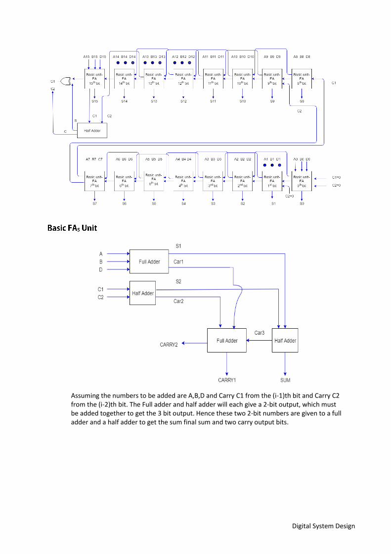
Here the 16Bit addition on the top level is the root problem. It gets subdivided at each level till we come till one bit addition. That is performed by FA5 unit. Hence we get 16bit sum(S) with 2carriers (C1 and C2).

Digital System Design
In this design, the 16bit number is brought to 1bit addition using FA5. Every (i+1)th addition must wait for the result from ith sub problem. Simple layout is shown below: The sub problem A1 waits for the result from sub problem A2. As soon as it generates C1 and C2 to the sub problem A1, it starts processing. Using a stitch up function the 16 bit addition can be achieved.
The 16bit addition using FA5 units is shown below. The c1 of 7th bit is given to 8th bit addition and c2 from the 6th bit is given to 8th bit addition. Since the 0th bit doesn’t have carry ins, both c1 and c2 are assigned 0. For the 1st bit it receives c1 from the 0th bit. However the c2 is set 0 for the 1st bit. Every FA5 block gives out one bit sum(S). But in the final bit the c1 from 15th bit and the c2 from the 14th bit is added using a Half adder. The carry from the Half adder is the final C1 and the sum from the half adder is given into an or gate. The input for the OR gate the c2 from the 15th bit. This will generate the final C2.
Digital System Design
Assuming the numbers to be added are A,B,D and Carry C1 from the (i-1)th bit and Carry C2 from the (i-2)th bit. The Full adder and half adder will each give a 2-bit output, which must be added together to get the 3 bit output. Hence these two 2-bit numbers are given to a full adder and a half adder to get the sum final sum and two carry output bits.

Digital System Design
Total number of inputs in 1- FA5 = 5inputs Total input units = 16*FA5 + 1 HA + 1 OR gate = 80+2+2= 84inputs.
(i) 16Bit circuit: Delay of 1FA5 = 2FA+1HA (critical path) = 5p+5p+2p=12p Total delay of the 16bit circuit = 16*FA5 + 1HA + 1XOR=160p+2p+2p= 196p. (ii) n-Bit circuit:
delay for n-bit 3numbers addition will be n(FA5) + 1 HA + 1 XOR=(12n+4)p
(i) 16Bit circuit: 16Fa5+1HA+1XOR=18units
(ii) N-bit circuit Total basic components required= n(FA5)+ 1 HA + 1 OR= (n+2)basic units.
The numbers A,B and D are added using full adder which will give us S1=1 Car1=1. The Carries C1=1 and C2=1 are separately added which will give us S2=0 Car2=1. Now the S1Car1 must be added with S2Car2. In the Half adder the S1=1 and S2=0 will be added which will give SUM=1 and Car3=0. The Car1=1 and Car2=1 are added in full adder along with Car3=0. This will give us CARRY1=0 and CARRY2=1. That’s the output of FA5
Digital System Design
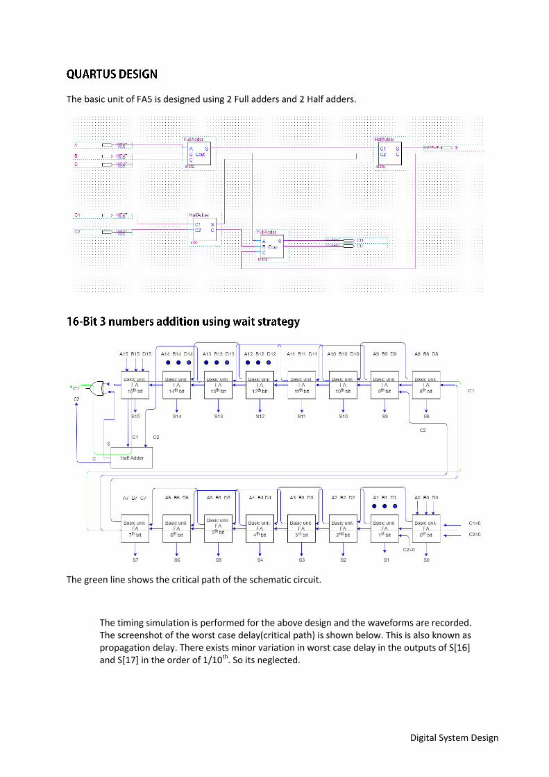
The basic unit of FA5 is designed using 2 Full adders and 2 Half adders.
The green line shows the critical path of the schematic circuit.
The timing simulation is performed for the above design and the waveforms are recorded. The screenshot of the worst case delay(critical path) is shown below. This is also known as propagation delay. There exists minor variation in worst case delay in the outputs of S[16] and S[17] in the order of 1/10th. So its neglected.

Digital System Design
Propagation delay(Ts) = 25.568ns
T = 13.767ns (As defined in the question. Refer the screenshot to verify the correctness)
Hence AT2= 84*13.7672=15920.94 units. (A is calculated in the previous page)

Digital System Design
Digital System Design
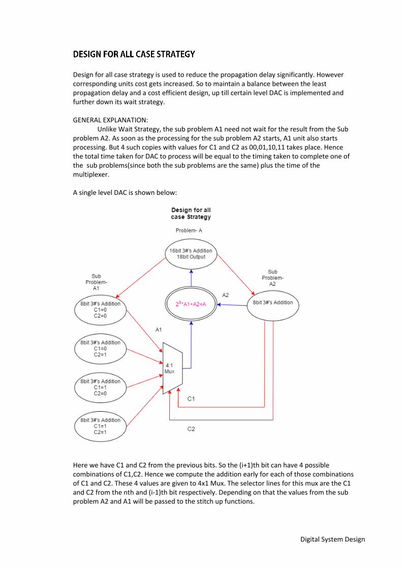
Design for all case strategy is used to reduce the propagation delay significantly. However corresponding units cost gets increased. So to maintain a balance between the least propagation delay and a cost efficient design, up till certain level DAC is implemented and further down its wait strategy. GENERAL EXPLANATION: Unlike Wait Strategy, the sub problem A1 need not wait for the result from the Sub problem A2. As soon as the processing for the sub problem A2 starts, A1 unit also starts processing. But 4 such copies with values for C1 and C2 as 00,01,10,11 takes place. Hence the total time taken for DAC to process will be equal to the timing taken to complete one of the sub problems(since both the sub problems are the same) plus the time of the multiplexer. A single level DAC is shown below:
Here we have C1 and C2 from the previous bits. So the (i+1)th bit can have 4 possible combinations of C1,C2. Hence we compute the addition early for each of those combinations of C1 and C2. These 4 values are given to 4x1 Mux. The selector lines for this mux are the C1 and C2 from the nth and (i-1)th bit respectively. Depending on that the values from the sub problem A2 and A1 will be passed to the stitch up functions.

Digital System Design
As said earlier, in order to reduce the propagation delays as well as to make the circuit cost efficient, we incorporate DAC till certain level and Wait strategy till certain level. Using the
formula given, the level J is determined. The group size x= √n
Level j = log(n/x opt) = logn−log(x opt) =log (16/4) =log16-log4=4—2=2. Hence we use DAC to the first two level, then wait strategy for the rest of the levels.
Digital System Design
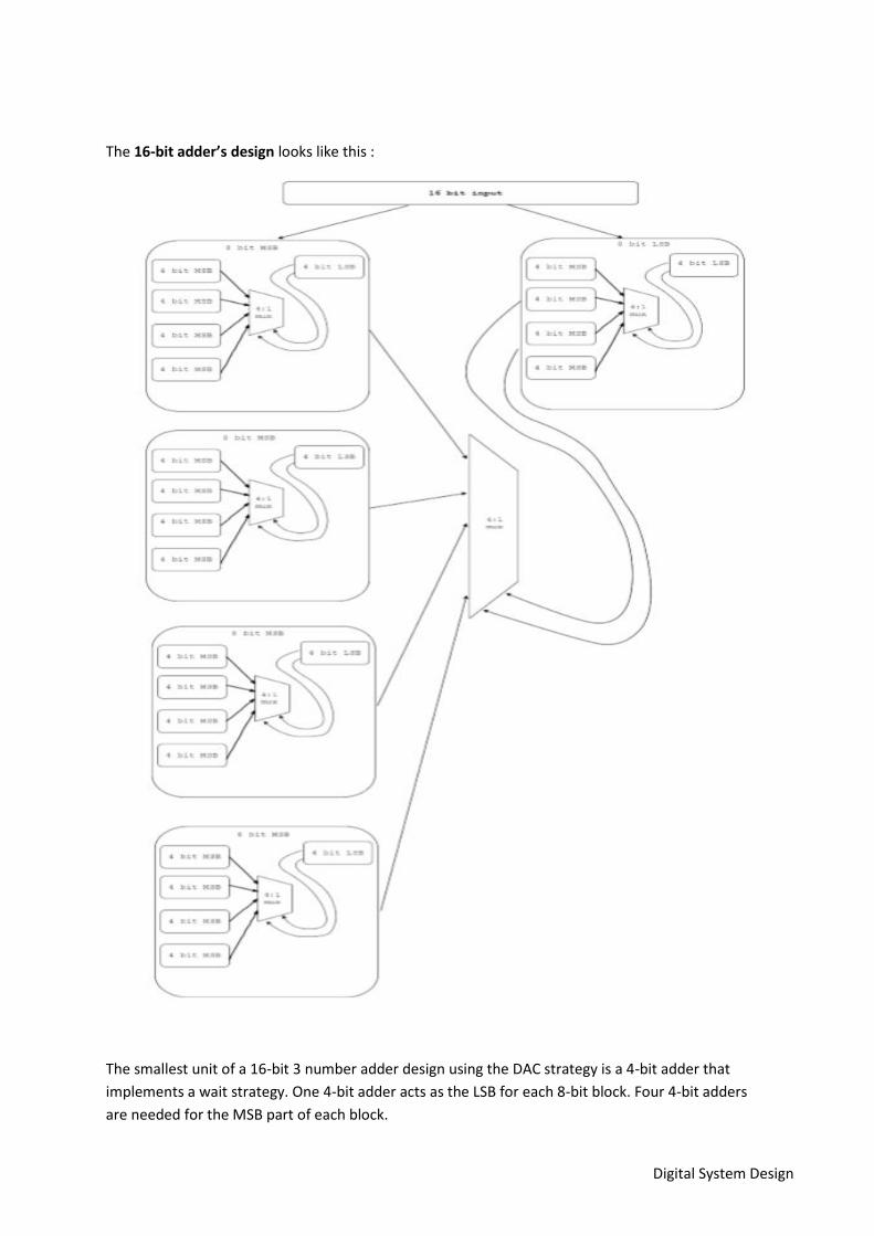
The 16-bit adder’s design looks like this :
The smallest unit of a 16-bit 3 number adder design using the DAC strategy is a 4-bit adder that
implements a wait strategy. One 4-bit adder acts as the LSB for each 8-bit block. Four 4-bit adders
are needed for the MSB part of each block.
Digital System Design
Each 4-bit adder is fed with three 4-bit input buses and 3 carry-ins. As we know from the 3 number
addition, there can be two carries per column. The output of each 4-bit adder block is a 4-bit sum
output fed into a bus S[3..0] and 2 carry outs C1 and C2.
We know, in the wait strategy, the carry out C1 from ith adder is fed to the (i+1)th bit adder and the
C2 from ith adder is fed to the (i+2)th adder. In our 4-bit adder, likewise the C2 from the third adder
should be fed to the fifth bit and the C1 from the 4th adder should also be fed to the fifth bit. To have
two output from the 4 bit wait block, we add these two bits using a half adder. The Sum of this half
adder acts as C1 input for the fifth bit and the Carry out of this half adder is given as an input to the
XOR gate along with the C2 of the 4th bit to generate the Carry(C2) for the sixth bit.
The 4-bit adder(LSB) is fed with 3 4-bit, input buses. The carry ins In1, In2 and In3 are zero. The MSB
part contains 4 similar adders. Each have 3 4-bit input buses. The In2 pin of each MSB block is
grounded as there is no C2 for the first bit of the MSB. The values in1 and In3 for each MSB block is
different and is either 00,01,10 or 11. There is a 4:1 mux to select 1 out of the 4 MSB blocks. The
mux is fed with the carry outs from the LSB. On the basis of theses carry outs one MSB block is
selected. From this 8 bit block, we get an 8 bit sum fed into a bus S[7..0] and two carry outs C1 and
c2.
As we can see from the diagram we have 1 8-bit LSB and 4 8-bit MSB blocks.
The 8-bit block is fed with input buses A, B and D and two carry ins In1 and In2. Each 8-bit block gives
8 bit SUM S[7..0] and two carry outs.
The LSB 8-bit block has its carry in pins grounded as there is no carry ins to the first and the second
bit. There are four 8 bit blocks. The design is similar to the 8-bit block design which consisted of 4-bit
LSB and four 4-bit MSB. The multiplexer is fed with the carry outs form the LSB. On the basis of these
Carry outs one out of the four MSBs are selected. The output from this level would be the 16-bit sum
and 2 carry out bits. As this is the last level, the carry outs would be fed into the output bus along
with the 16-bit Sum, thus giving an 18-bit sum for the three 16-bit inputs.
Number of inputs in 1-4Bit WS= 20+2+2=24inputs Number of inputs in 1-4x1 Mux= 6inputs Total area of 16Bit Circuit= 25*24 + 6*6=636inputs
(i) For 16Bit 3numbers addition:
Delay of 4Bit W.S = 4*10p+1HA+1XOR=44p Delay of 4x1 Mux=6p Total delay of the 16bit circuit =44+ 2(4x1 MUX)= 44+12=56p

Digital System Design
(ii) For n-bit 3numbers addition: Delay= x(Delay of FA5)+(n/x -1)(Delay of 4x1 MUX) X=group size.
For 16Bit 3numbers addition: Basic units in 1-4B W.S=4FA5+1XOR+1HA=6units Total number of basic units in 16Bit DAC=25*4B W.S+5MUX1 +1MUX2=156units.
Digital System Design
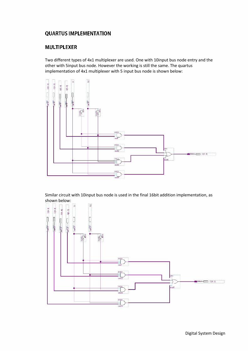
Two different types of 4x1 multiplexer are used. One with 10input bus node entry and the other with 5input bus node. However the working is still the same. The quartus implementation of 4x1 multiplexer with 5 input bus node is shown below:
Similar circuit with 10input bus node is used in the final 16bit addition implementation, as shown below:

Digital System Design
The 4bit wait strategy addition of 3 numbers is shown below. This is a simple wait strategy addition wherein the C1 and C2 of the ith bit addition block is given to (i+1)th and (i+2)th FA5. The C1 and C2 for the last 2bit addition differ depending upon the previous sub problem. For the inputs from [0..3] the C1 C2 and C2 of the 0th and 1st bit FA5 unit will be zero.
Now this is blocked up into a single unit with arrays of inputs being A[3..0],B[3..0],D[3..0] and output S[3..0] with C1 and C2. The next level is the DAC implementation.
We know, in the wait strategy, the carry out C1 from each single bit adder is fed to the (i+1)th adder
and the C2 from each single bit adder is fed to (i+2)th adder. In our 4-bit adder, the C2 from the third
adder should be fed to the fifth bit and the C1 from the 4th adder should also be fed to the fifth bit.
To minimize the inputs for the block level implementation of the 4-bit adder we add these two bits
using a half adder. The Sum of this half adder acts as C1 input for the fifth bit and the Carry out of
this half adder is XOR’ed with the C2 of the 4th bit to get the Carry for the sixth bit.

Digital System Design
:

Digital System Design
:
Digital System Design
:
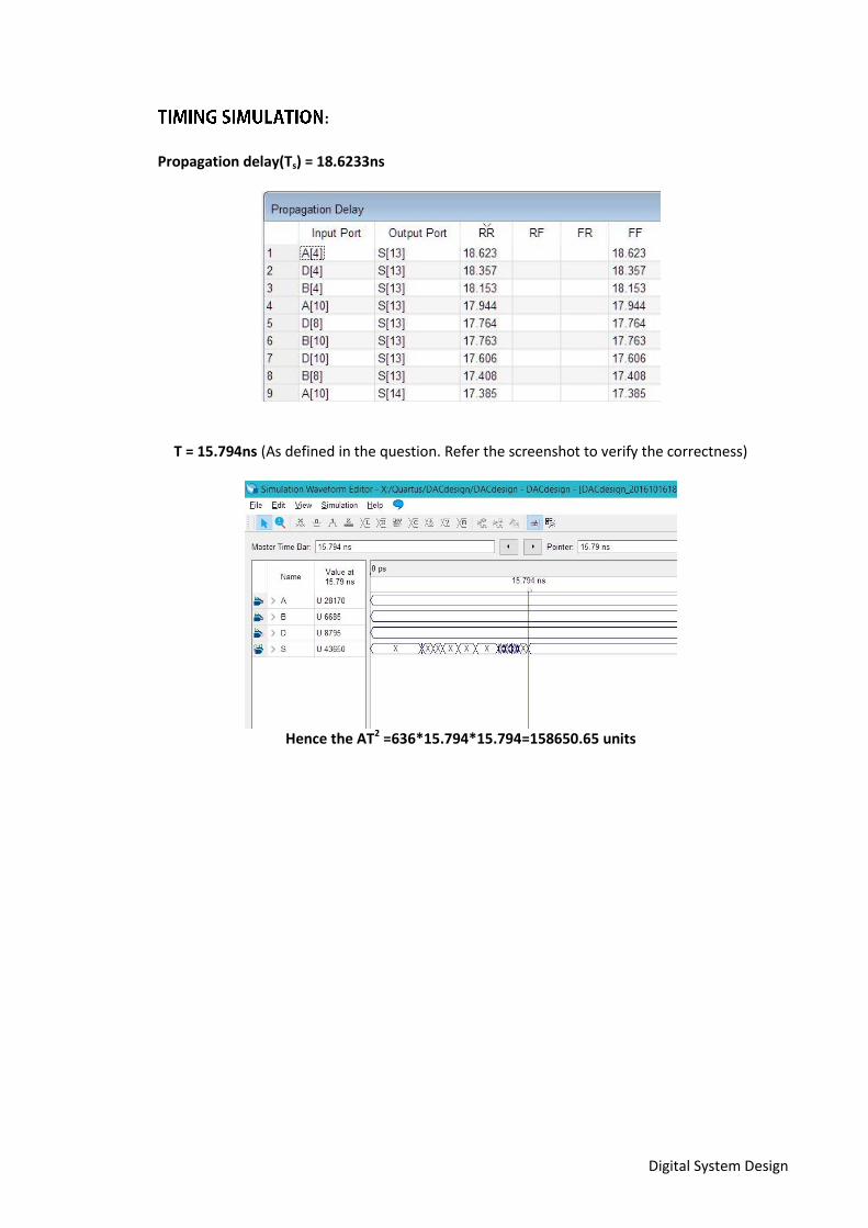
Propagation delay(Ts) = 18.6233ns
T = 15.794ns (As defined in the question. Refer the screenshot to verify the correctness)
Hence the AT2 =636*15.794*15.794=158650.65 units

Digital System Design

Digital System Design
It can be seen that the above designed circuits produce proper results for every type of input numbers. From the waveform graph it is clear that the Ts and T are not the same.
TYPE T(As defined..)[ns] AT2 Ts[ns]
1.WAIT STRATEGY 13.767 15920.94 units 25.568
2.DAC STRATEGY 15.794 158650.65 units 18.623
From the above table we can conclude that the propagation delay for the DAC strategy is less than that of the Wait strategy, but it comes with a higher cost.