ECE 429 Introduction to VLSI Design Lecture 05 CMOS …jwang/ece429-2018s/ece429-lec05.pdf · ECE...
60
ECE 429 – Introduction to VLSI Design Lecture 05 CMOS Layout and Fabrication Professor Jia Wang Department of Electrical and Computer Engineering Illinois Institute of Technology January 23, 2018 ECE 429 – Introduction to VLSI Design Spring 2018 1/24
Transcript of ECE 429 Introduction to VLSI Design Lecture 05 CMOS …jwang/ece429-2018s/ece429-lec05.pdf · ECE...

ECE 429 – Introduction to VLSI DesignLecture 05 CMOS Layout and Fabrication
Professor Jia WangDepartment of Electrical and Computer Engineering
Illinois Institute of Technology
January 23, 2018
ECE 429 – Introduction to VLSI Design Spring 2018 1/24
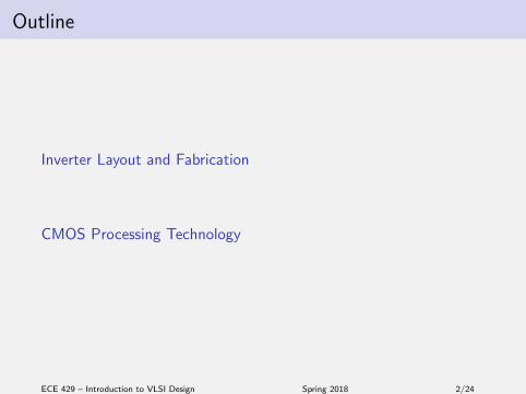
Outline
Inverter Layout and Fabrication
CMOS Processing Technology
ECE 429 – Introduction to VLSI Design Spring 2018 2/24

Reading Assignment
I This lecture: 1.5, 3
I Next lecture: 1.5
ECE 429 – Introduction to VLSI Design Spring 2018 3/24

Outline
Inverter Layout and Fabrication
CMOS Processing Technology
ECE 429 – Introduction to VLSI Design Spring 2018 4/24
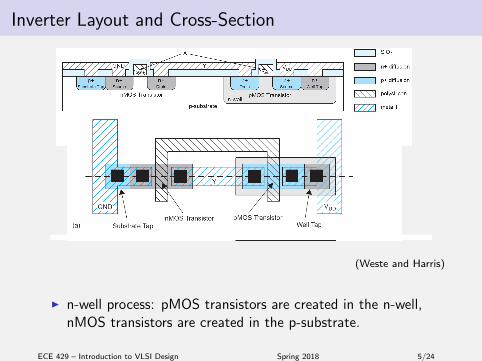
Inverter Layout and Cross-Section
(Weste and Harris)
I n-well process: pMOS transistors are created in the n-well,nMOS transistors are created in the p-substrate.
ECE 429 – Introduction to VLSI Design Spring 2018 5/24

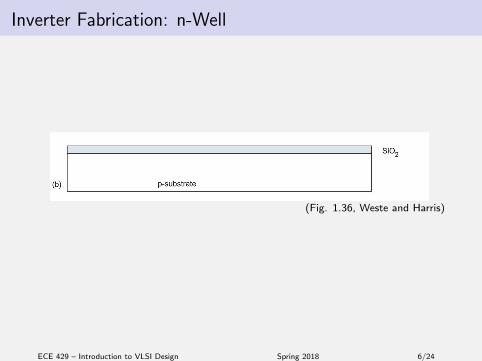
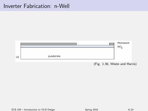
Inverter Fabrication: n-Well
(Fig. 1.36, Weste and Harris)
ECE 429 – Introduction to VLSI Design Spring 2018 6/24
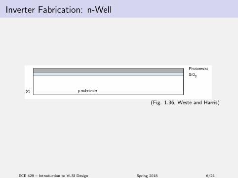
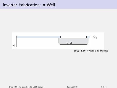
Inverter Fabrication: n-Well
(Fig. 1.36, Weste and Harris)
ECE 429 – Introduction to VLSI Design Spring 2018 6/24
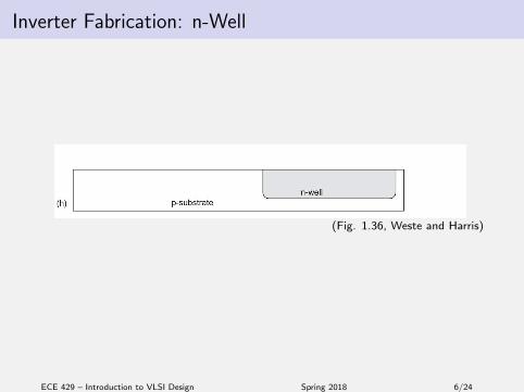
Inverter Fabrication: n-Well
(Fig. 1.36, Weste and Harris)
ECE 429 – Introduction to VLSI Design Spring 2018 6/24
Inverter Fabrication: n-Well
(Fig. 1.36, Weste and Harris)
ECE 429 – Introduction to VLSI Design Spring 2018 6/24

Inverter Fabrication: n-Well
(Fig. 1.36, Weste and Harris)
ECE 429 – Introduction to VLSI Design Spring 2018 6/24

Inverter Fabrication: n-Well
(Fig. 1.36, Weste and Harris)
ECE 429 – Introduction to VLSI Design Spring 2018 6/24
Inverter Fabrication: n-Well
(Fig. 1.36, Weste and Harris)
ECE 429 – Introduction to VLSI Design Spring 2018 6/24
Inverter Fabrication: n-Well
(Fig. 1.36, Weste and Harris)
ECE 429 – Introduction to VLSI Design Spring 2018 6/24

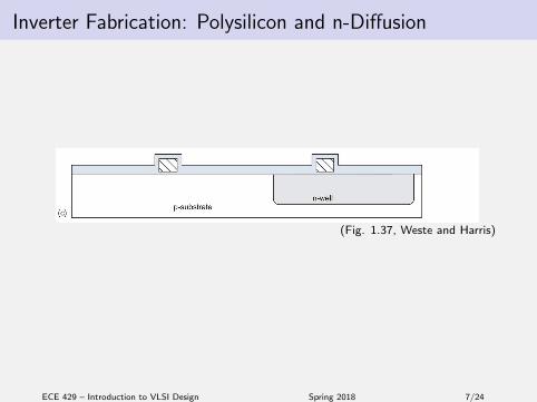
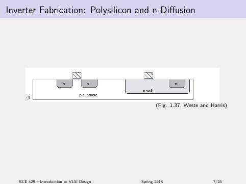
Inverter Fabrication: Polysilicon and n-Diffusion
(Fig. 1.37, Weste and Harris)
ECE 429 – Introduction to VLSI Design Spring 2018 7/24

Inverter Fabrication: Polysilicon and n-Diffusion
(Fig. 1.37, Weste and Harris)
ECE 429 – Introduction to VLSI Design Spring 2018 7/24
Inverter Fabrication: Polysilicon and n-Diffusion
(Fig. 1.37, Weste and Harris)
ECE 429 – Introduction to VLSI Design Spring 2018 7/24

Inverter Fabrication: Polysilicon and n-Diffusion
(Fig. 1.37, Weste and Harris)
ECE 429 – Introduction to VLSI Design Spring 2018 7/24

Inverter Fabrication: Polysilicon and n-Diffusion
(Fig. 1.37, Weste and Harris)
ECE 429 – Introduction to VLSI Design Spring 2018 7/24
Inverter Fabrication: Polysilicon and n-Diffusion
(Fig. 1.37, Weste and Harris)
ECE 429 – Introduction to VLSI Design Spring 2018 7/24
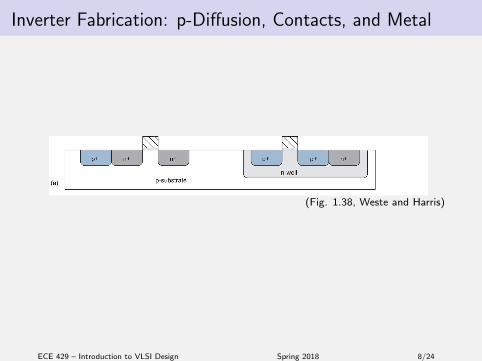
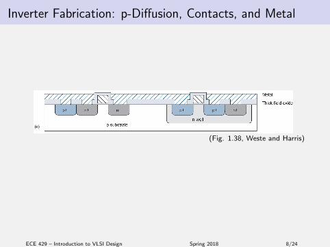
Inverter Fabrication: p-Diffusion, Contacts, and Metal
(Fig. 1.38, Weste and Harris)
ECE 429 – Introduction to VLSI Design Spring 2018 8/24

Inverter Fabrication: p-Diffusion, Contacts, and Metal
(Fig. 1.38, Weste and Harris)
ECE 429 – Introduction to VLSI Design Spring 2018 8/24
Inverter Fabrication: p-Diffusion, Contacts, and Metal
(Fig. 1.38, Weste and Harris)
ECE 429 – Introduction to VLSI Design Spring 2018 8/24
Outline
Inverter Layout and Fabrication
CMOS Processing Technology
ECE 429 – Introduction to VLSI Design Spring 2018 9/24

Inverter Layout and Cross-Section
(Weste and Harris)
I n-well process: pMOS transistors are created in the n-well,nMOS transistors are created in the p-substrate.
ECE 429 – Introduction to VLSI Design Spring 2018 10/24

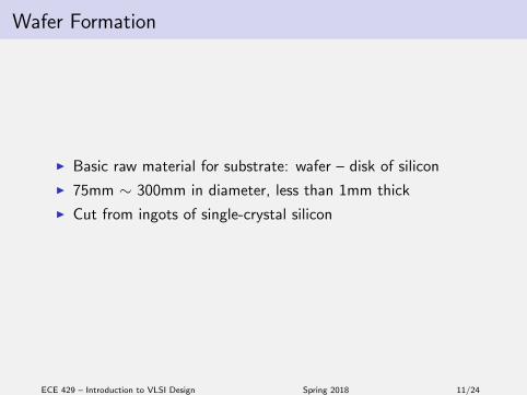
Wafer Formation
I Basic raw material for substrate: wafer – disk of silicon
I 75mm ∼ 300mm in diameter, less than 1mm thick
I Cut from ingots of single-crystal silicon
ECE 429 – Introduction to VLSI Design Spring 2018 11/24

Wafer Formation
I Basic raw material for substrate: wafer – disk of silicon
I 75mm ∼ 300mm in diameter, less than 1mm thick
I Cut from ingots of single-crystal silicon
ECE 429 – Introduction to VLSI Design Spring 2018 11/24
Wafer Formation
I Basic raw material for substrate: wafer – disk of silicon
I 75mm ∼ 300mm in diameter, less than 1mm thick
I Cut from ingots of single-crystal silicon
ECE 429 – Introduction to VLSI Design Spring 2018 11/24
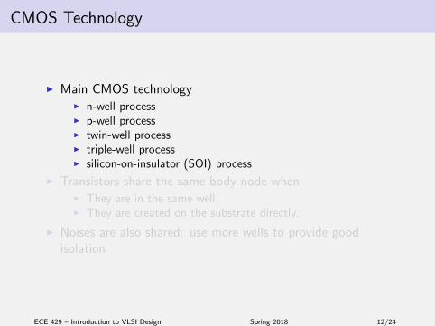
CMOS Technology
I Main CMOS technologyI n-well processI p-well processI twin-well processI triple-well processI silicon-on-insulator (SOI) process
I Transistors share the same body node whenI They are in the same well.I They are created on the substrate directly.
I Noises are also shared: use more wells to provide goodisolation
ECE 429 – Introduction to VLSI Design Spring 2018 12/24
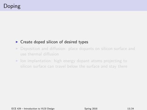
Doping
I Create doped silicon of desired types
I Deposition and diffusion: place dopants on silicon surface anduse thermal diffusion
I Ion implantation: high energy dopant atoms projecting tosilicon surface can travel below the surface and stay there
ECE 429 – Introduction to VLSI Design Spring 2018 13/24

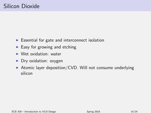
Silicon Dioxide
I Essential for gate and interconnect isolation
I Easy for growing and etching
I Wet oxidation: water
I Dry oxidation: oxygen
I Atomic layer deposition/CVD. Will not consume underlyingsilicon
ECE 429 – Introduction to VLSI Design Spring 2018 14/24

Silicon Dioxide
I Essential for gate and interconnect isolation
I Easy for growing and etching
I Wet oxidation: water
I Dry oxidation: oxygen
I Atomic layer deposition/CVD. Will not consume underlyingsilicon
ECE 429 – Introduction to VLSI Design Spring 2018 14/24

Silicon Dioxide
I Essential for gate and interconnect isolation
I Easy for growing and etching
I Wet oxidation: water
I Dry oxidation: oxygen
I Atomic layer deposition/CVD. Will not consume underlyingsilicon
ECE 429 – Introduction to VLSI Design Spring 2018 14/24

Silicon Dioxide
I Essential for gate and interconnect isolation
I Easy for growing and etching
I Wet oxidation: water
I Dry oxidation: oxygen
I Atomic layer deposition/CVD. Will not consume underlyingsilicon
ECE 429 – Introduction to VLSI Design Spring 2018 14/24
Silicon Dioxide
I Essential for gate and interconnect isolation
I Easy for growing and etching
I Wet oxidation: water
I Dry oxidation: oxygen
I Atomic layer deposition/CVD. Will not consume underlyingsilicon
ECE 429 – Introduction to VLSI Design Spring 2018 14/24
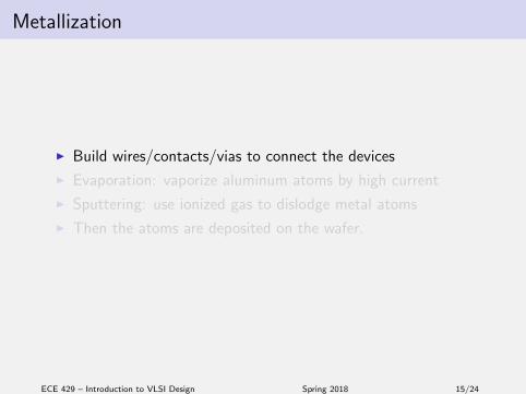
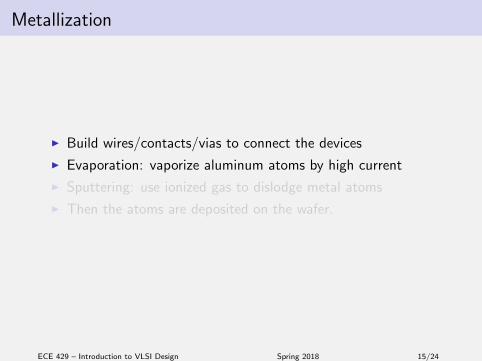
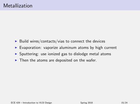
Metallization
I Build wires/contacts/vias to connect the devices
I Evaporation: vaporize aluminum atoms by high current
I Sputtering: use ionized gas to dislodge metal atoms
I Then the atoms are deposited on the wafer.
ECE 429 – Introduction to VLSI Design Spring 2018 15/24
Metallization
I Build wires/contacts/vias to connect the devices
I Evaporation: vaporize aluminum atoms by high current
I Sputtering: use ionized gas to dislodge metal atoms
I Then the atoms are deposited on the wafer.
ECE 429 – Introduction to VLSI Design Spring 2018 15/24

Metallization
I Build wires/contacts/vias to connect the devices
I Evaporation: vaporize aluminum atoms by high current
I Sputtering: use ionized gas to dislodge metal atoms
I Then the atoms are deposited on the wafer.
ECE 429 – Introduction to VLSI Design Spring 2018 15/24
Metallization
I Build wires/contacts/vias to connect the devices
I Evaporation: vaporize aluminum atoms by high current
I Sputtering: use ionized gas to dislodge metal atoms
I Then the atoms are deposited on the wafer.
ECE 429 – Introduction to VLSI Design Spring 2018 15/24

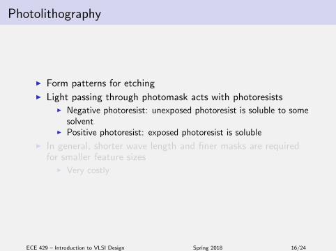
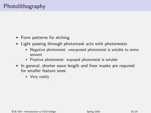
Photolithography
I Form patterns for etchingI Light passing through photomask acts with photoresists
I Negative photoresist: unexposed photoresist is soluble to somesolvent
I Positive photoresist: exposed photoresist is soluble
I In general, shorter wave length and finer masks are requiredfor smaller feature sizes
I Very costly
ECE 429 – Introduction to VLSI Design Spring 2018 16/24
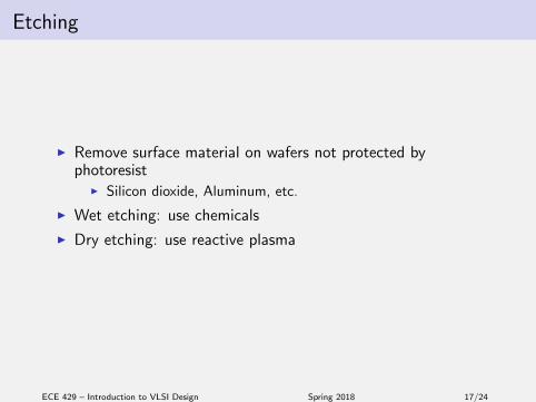
Etching
I Remove surface material on wafers not protected byphotoresist
I Silicon dioxide, Aluminum, etc.
I Wet etching: use chemicals
I Dry etching: use reactive plasma
ECE 429 – Introduction to VLSI Design Spring 2018 17/24

Etching
I Remove surface material on wafers not protected byphotoresist
I Silicon dioxide, Aluminum, etc.
I Wet etching: use chemicals
I Dry etching: use reactive plasma
ECE 429 – Introduction to VLSI Design Spring 2018 17/24
Etching
I Remove surface material on wafers not protected byphotoresist
I Silicon dioxide, Aluminum, etc.
I Wet etching: use chemicals
I Dry etching: use reactive plasma
ECE 429 – Introduction to VLSI Design Spring 2018 17/24
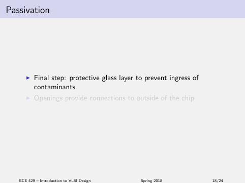
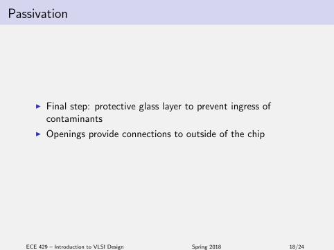
Passivation
I Final step: protective glass layer to prevent ingress ofcontaminants
I Openings provide connections to outside of the chip
ECE 429 – Introduction to VLSI Design Spring 2018 18/24
Passivation
I Final step: protective glass layer to prevent ingress ofcontaminants
I Openings provide connections to outside of the chip
ECE 429 – Introduction to VLSI Design Spring 2018 18/24
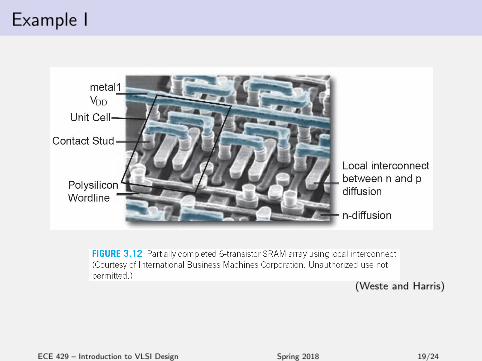
Example I
(Weste and Harris)
ECE 429 – Introduction to VLSI Design Spring 2018 19/24
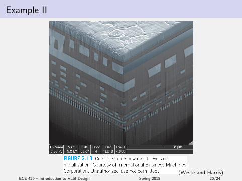
Example II
(Weste and Harris)ECE 429 – Introduction to VLSI Design Spring 2018 20/24

Example III
(Weste and Harris)
ECE 429 – Introduction to VLSI Design Spring 2018 21/24
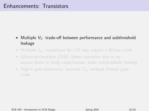
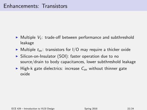
Enhancements: Transistors
I Multiple Vt : trade-off between performance and subthresholdleakage
I Multiple tox : transistors for I/O may require a thicker oxide
I Silicon-on-Insulator (SOI): faster operation due to nosource/drain to body capacitances, lower subthreshold leakage
I High-k gate dielectrics: increase Cox without thinner gateoxide
ECE 429 – Introduction to VLSI Design Spring 2018 22/24

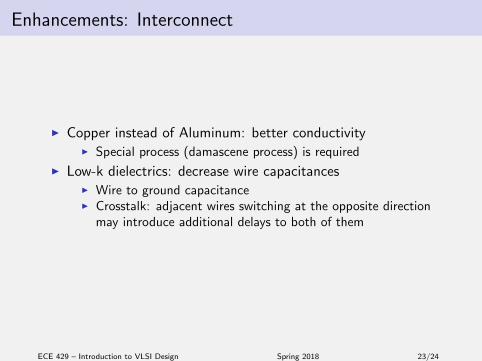
Enhancements: Interconnect
I Copper instead of Aluminum: better conductivityI Special process (damascene process) is required
I Low-k dielectrics: decrease wire capacitancesI Wire to ground capacitanceI Crosstalk: adjacent wires switching at the opposite direction
may introduce additional delays to both of them
ECE 429 – Introduction to VLSI Design Spring 2018 23/24

Summary
I Inverter layout and fabrication
I CMOS processing technology
ECE 429 – Introduction to VLSI Design Spring 2018 24/24