ECE 424 – Introduction to VLSI Design Emre Yengel Department of Electrical and Communication...
32
ECE 424 – Introduction to VLSI Design Emre Yengel Department of Electrical and Communication Engineering Fall 2014
-
Upload
wilson-codrington -
Category
Documents
-
view
223 -
download
0
Transcript of ECE 424 – Introduction to VLSI Design Emre Yengel Department of Electrical and Communication...
ECE 424 – Introduction to VLSI Design
Emre Yengel
Department of Electrical and Communication Engineering
Fall 2014
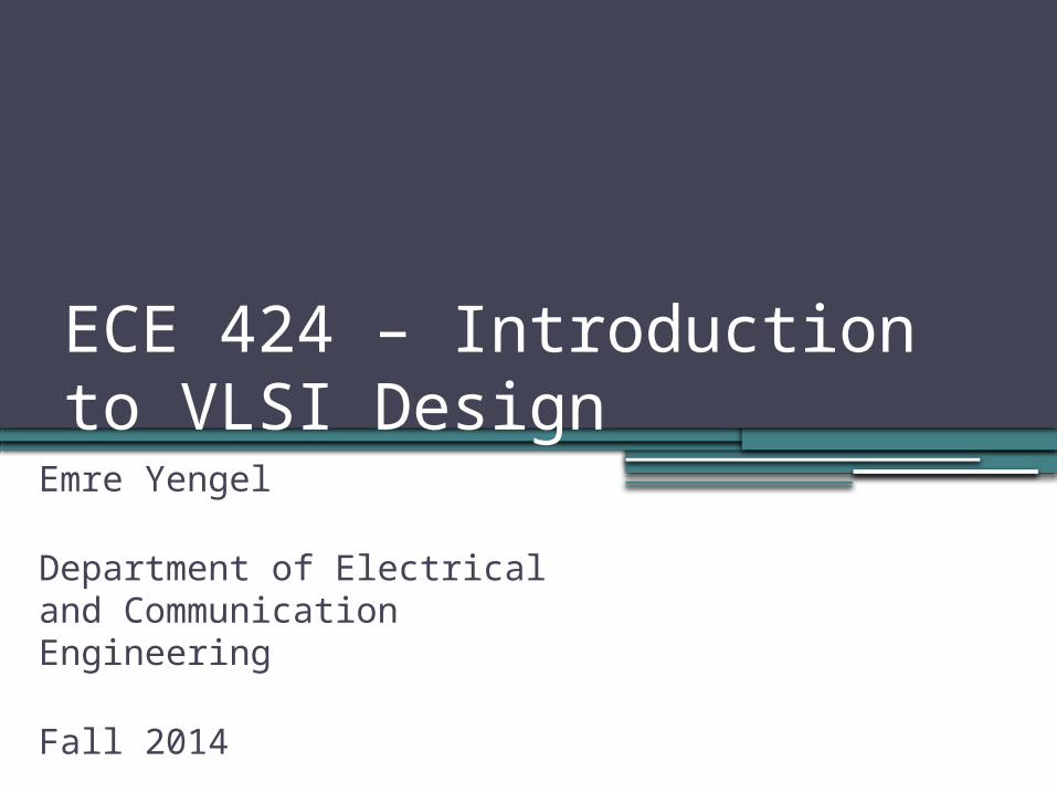
Introduction
• Sequential circuito Output depends not just on present inputs (as in
combinational circuit), but on past sequence of inputs• Stores bits, also known as having “state”
o Simple example: a circuit that counts up in binary
COMBINATIONALLOGIC
Registers
Outputs
Next state
CLK
Q D
Current State
Inputs
• A sequential circuit consists of a feedback path, and employs some memory elements.
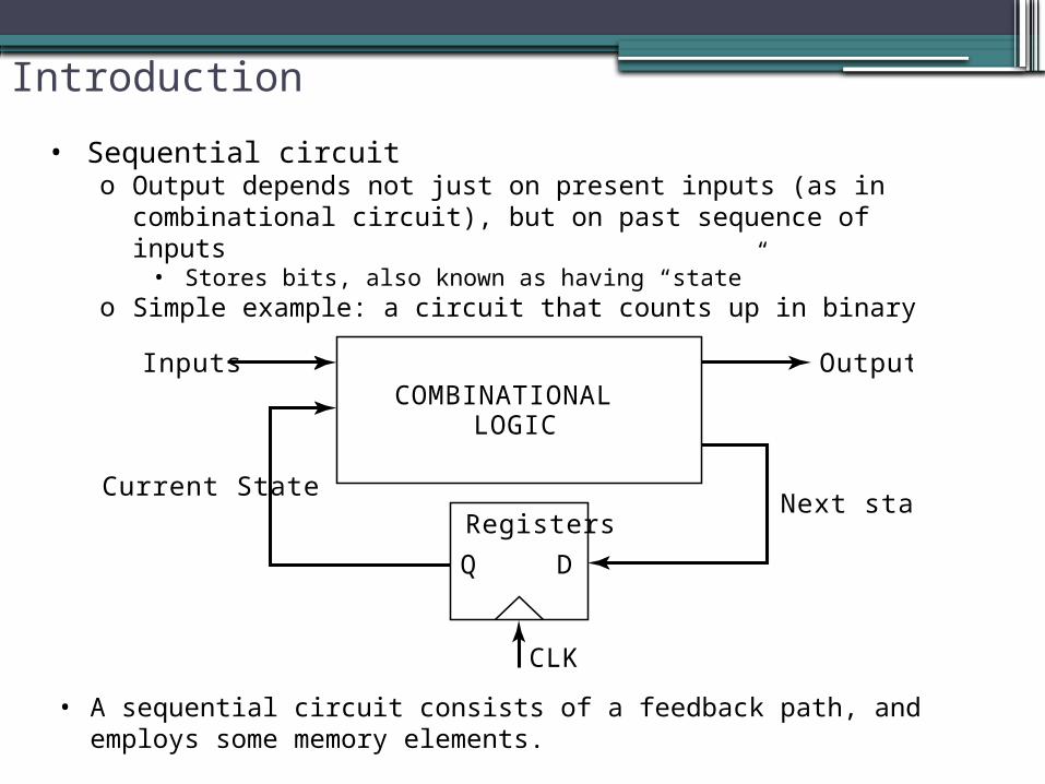
Introduction
a
•Flight attendant call button▫Press call: light turns on
Stays on after button released
▫Press cancel: light turns off
▫Logic gate circuit to implement this?
QCall
Cancel
Doesn’t work. Q=1 when Call=1, but doesn’t stay 1 when Call returns to 0
Need some form of “feedback” in the circuit
a
a
BitStorage
Blue lightCallbutton
Cancelbutton
1. Call button pressed – light turns on
BitStorage
Blue lightCallbutton
Cancelbutton
2. Call button released – light stays on
BitStorage
Blue lightCallbutton
Cancelbutton
3. Cancel button pressed – light turns off
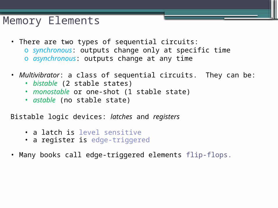
Memory Elements
• There are two types of sequential circuits:o synchronous: outputs change only at specific timeo asynchronous: outputs change at any time
• Multivibrator: a class of sequential circuits. They can be:• bistable (2 stable states)• monostable or one-shot (1 stable state)• astable (no stable state)
Bistable logic devices: latches and registers
• a latch is level sensitive• a register is edge-triggered
• Many books call edge-triggered elements flip-flops.
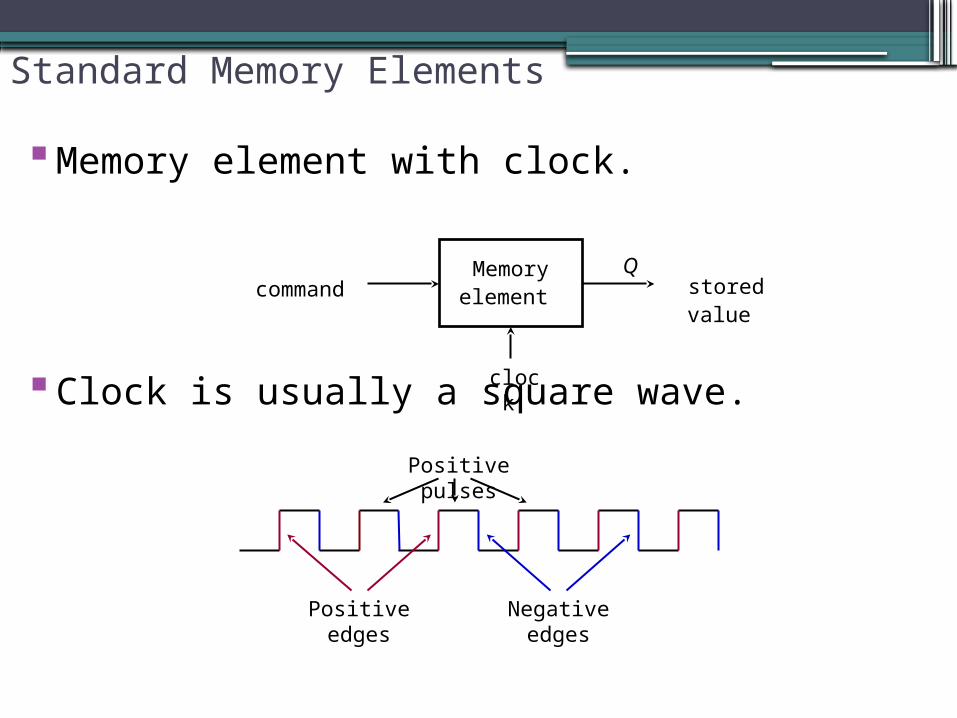
Standard Memory Elements
Memory element with clock.
Clock is usually a square wave.
command Memory element stored value
Q
clock
Positive edges Negative edges
Positive pulses
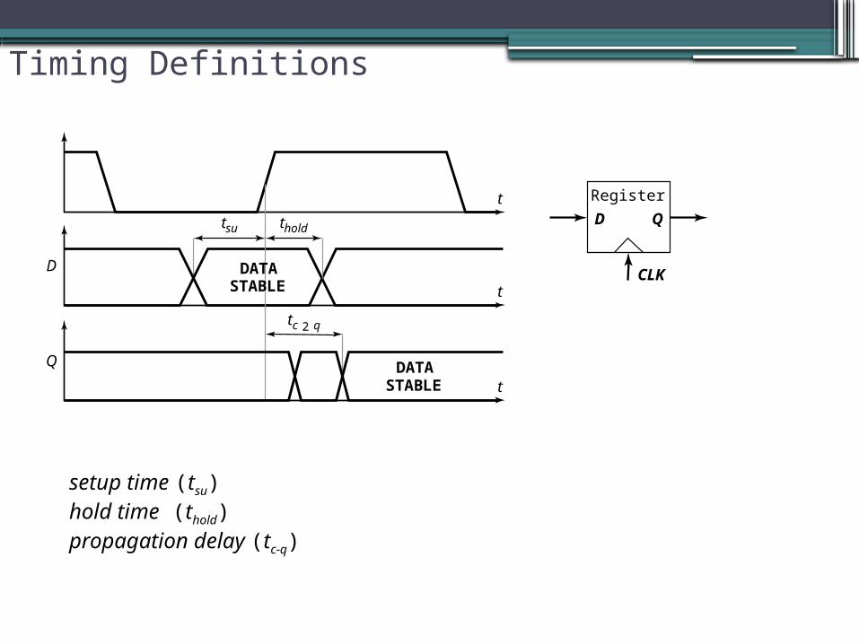
Timing Definitions
t
t
D
tc 2 q
tholdtsu
t
Q DATASTABLE
DATASTABLE
Register
CLK
D Q
setup time (tsu)hold time (thold)propagation delay (tc-
q)
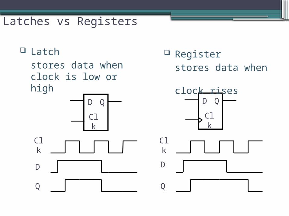
Latches vs Registers
Latch
stores data when clock is low or high
D
Clk
Q D
Clk
Q
Register
stores data when clock rises
Clk Clk
D D
Q Q
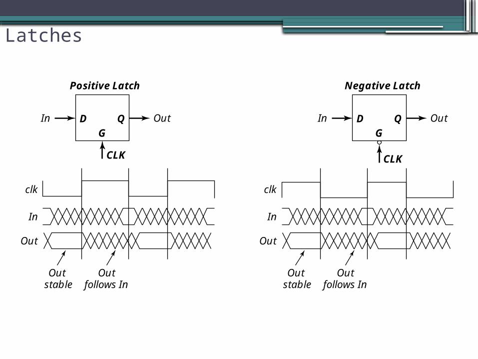
Latches
In
clk
In
Out
Positive Latch
CLK
DG
Q
Out
Outstable
Outfollows In
In
clk
In
Out
Negative Latch
CLK
DG
Q
Out
Outstable
Outfollows In
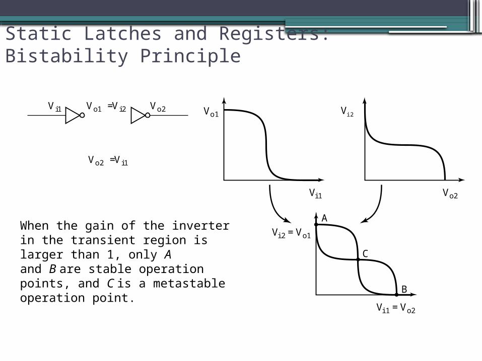
Static Latches and Registers: Bistability Principle
Vi1 Vo2
Vo2 =Vi1
Vo1 =Vi2
Vi1
A
C
B
Vo2
Vi1=Vo2
Vo1 Vi2
Vi2=Vo1When the gain of the inverter in the transient region is larger than 1, only Aand B are stable operation points, and C is a metastable operation point.
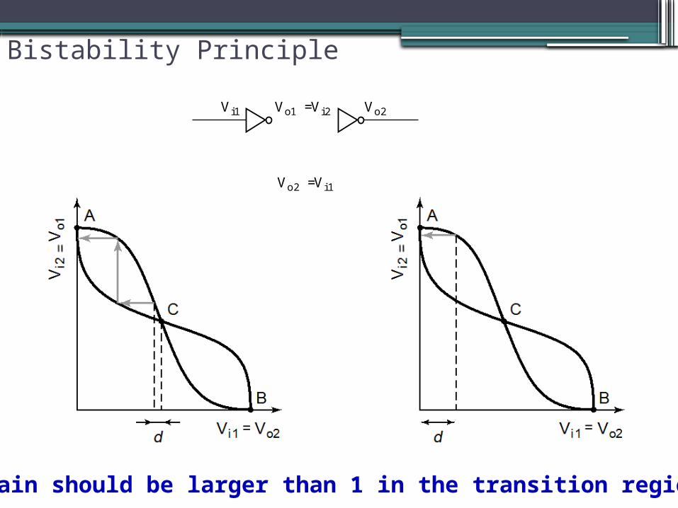
Gain should be larger than 1 in the transition region
Bistability Principle
Vi1 Vo2
Vo2 =Vi1
Vo1 =Vi2
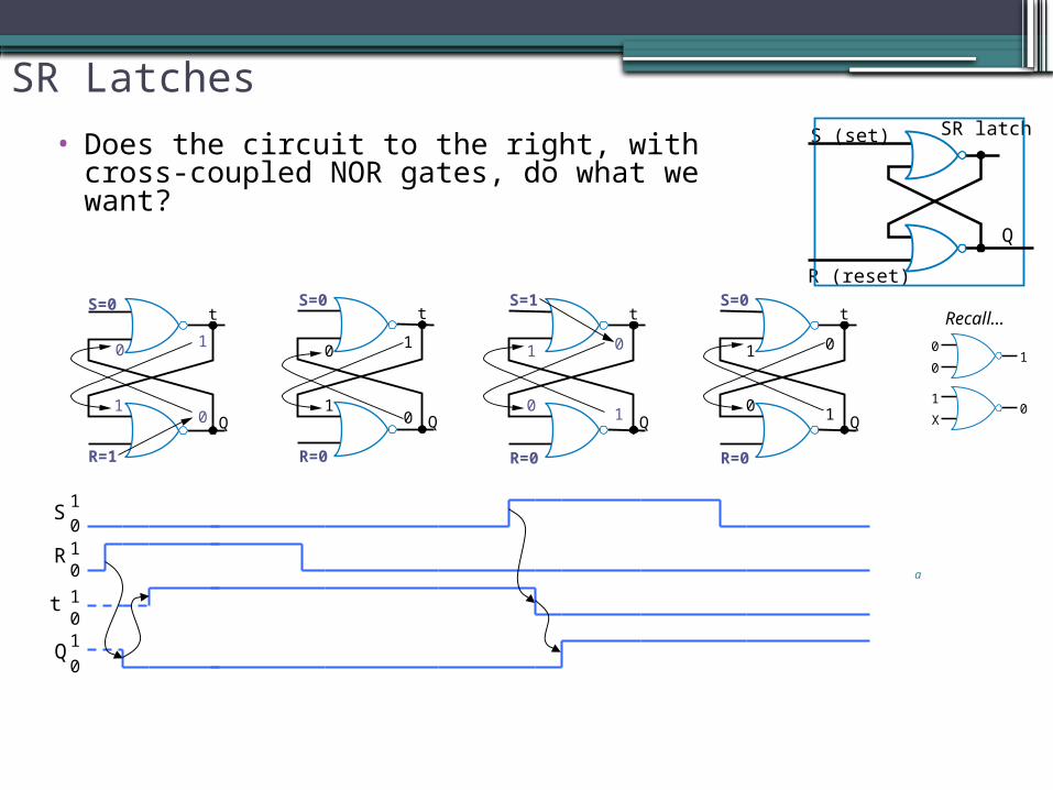
SR Latches
0
0
1
R=1
S=0t
Q
1
010
R
S
10
t
1
0Q
Q
S (set) SR latch
R (reset)
• Does the circuit to the right, with cross-coupled NOR gates, do what we want?
1
0 0
10
1
t
Q
S=0
R=0
t
Q
S=1
R=0
0
1
1
t
Q
R=0
S=0
1
01
0
0
01
1
X0
Recall…
a
SR Latches
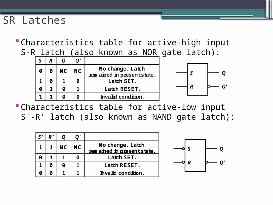
Characteristics table for active-high input S-R latch (also known as NOR gate latch):
Characteristics table for active-low input S'-R' latch (also known as NAND gate latch):
S R Q Q'
0 0 NC NC No change. Latchremained in present state.
1 0 1 0 Latch SET.
0 1 0 1 Latch RESET.
1 1 0 0 Invalid condition.
S' R' Q Q'
1 1 NC NC No change. Latchremained in present state.
0 1 1 0 Latch SET.
1 0 0 1 Latch RESET.
0 0 1 1 Invalid condition.
S
R
Q
Q'
S
R
Q
Q'
SR Latches
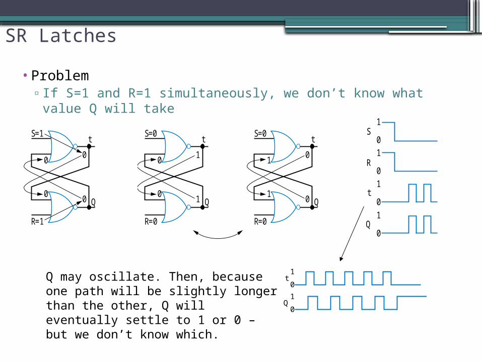
• Problem▫ If S=1 and R=1 simultaneously, we don’t know what value Q
will take
R=1
S=1
0
0
0
0
t
Q
R=0
S=0
0
0
1
1
t
Q
R=0
S=0
1
1
0
0
t
Q
0
1
0
1
0
1
0
1
S
R
Q
t
1t
0
1Q
0
Q may oscillate. Then, because one path will be slightly longer than the other, Q will eventually settle to 1 or 0 – but we don’t know which.
SR Latches
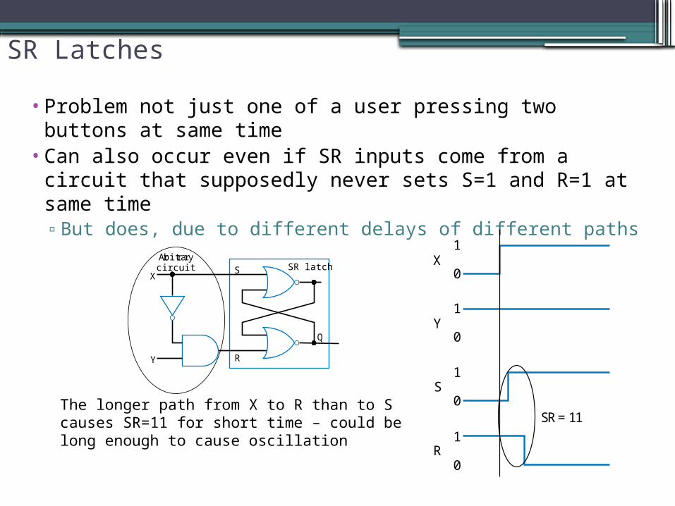
• Problem not just one of a user pressing two buttons at same time
• Can also occur even if SR inputs come from a circuit that supposedly never sets S=1 and R=1 at same time▫But does, due to different delays of different paths
1
0
1
0
1
0
1
0
X
Y
S
R
SR = 11The longer path from X to R than to S causes SR=11 for short time – could be long enough to cause oscillation
RY
XS SR latch
Q
Arbitrarycircuit
Level Sensitive SR Latches
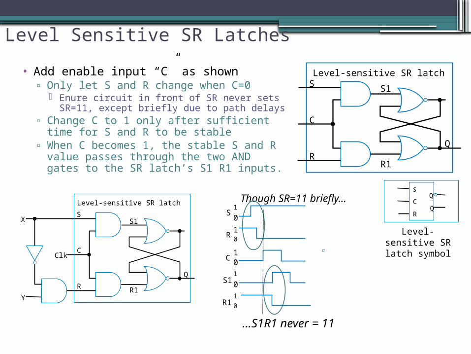
• Add enable input “C” as shown▫ Only let S and R change when C=0
Enure circuit in front of SR never sets SR=11, except briefly due to path delays
▫ Change C to 1 only after sufficient time for S and R to be stable
▫ When C becomes 1, the stable S and R value passes through the two AND gates to the SR latch’s S1 R1 inputs.
R1
S1S
C
R
Level-sensitive SR latch
Q
Though SR=11 briefly...
...S1R1 never = 11
S
CQ’
QR
Level-sensitive SR latch symbol
R1
S1S
X
Y
CClk
R
Level-sensitive SR latch
Q
01
01
0
1
0
1
0S
R
C
S1
R1
1
a
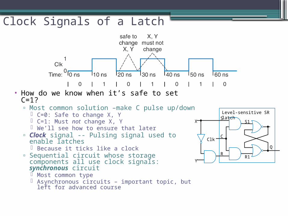
Clock Signals of a Latch
• How do we know when it’s safe to set C=1?▫ Most common solution –make C pulse up/down
C=0: Safe to change X, Y C=1: Must not change X, Y We’ll see how to ensure that later
▫ Clock signal -- Pulsing signal used to enable latches Because it ticks like a clock
▫ Sequential circuit whose storage components all use clock signals: synchronous circuit Most common type Asynchronous circuits – important topic, but left
for advanced course
R1
S1S
X
Y
CClk
R
Q
Level-sensitive SR latch
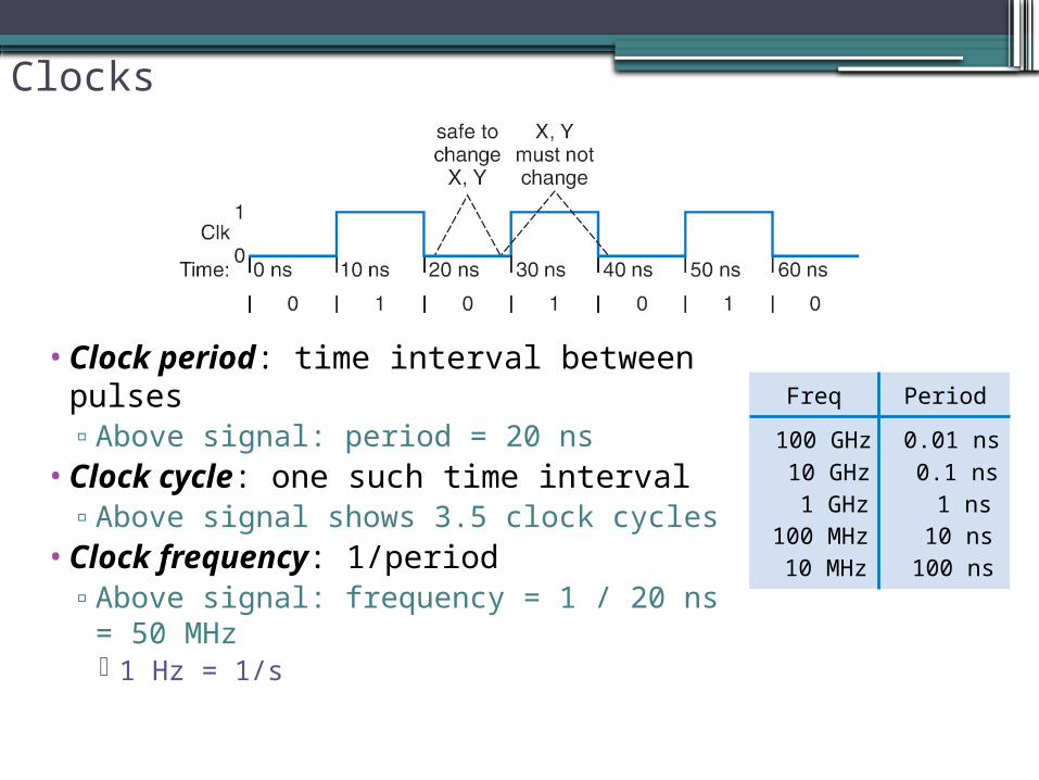
Clocks
• Clock period: time interval between pulses ▫Above signal: period = 20 ns
• Clock cycle: one such time interval▫Above signal shows 3.5 clock cycles
• Clock frequency: 1/period▫Above signal: frequency = 1 / 20 ns = 50
MHz 1 Hz = 1/s
100 GHz
10 GHz1 GHz
100 MHz10 MHz
0.01 ns
0.1 ns1 ns
10 ns100 ns
PeriodFreq
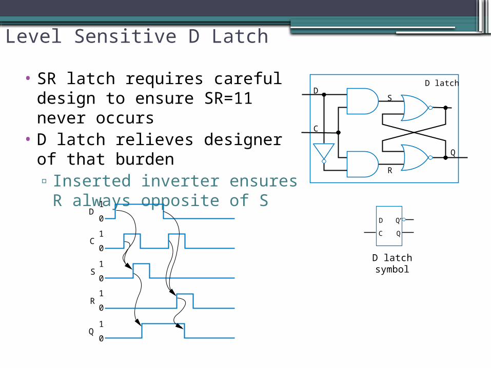
Level Sensitive D Latch
• SR latch requires careful design to ensure SR=11 never occurs
• D latch relieves designer of that burden▫Inserted inverter ensures R
always opposite of S
R
SD
C
D latch
Q
D Q’
QC
D latch symbol
1
0D
C
S
R
Q
1
0
1
0
1
0
1
0
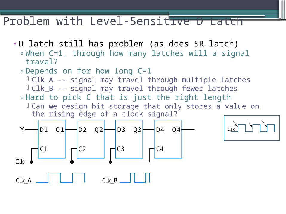
Problem with Level-Sensitive D Latch
• D latch still has problem (as does SR latch)▫When C=1, through how many latches will a signal travel?▫Depends on for how long C=1
Clk_A -- signal may travel through multiple latches Clk_B -- signal may travel through fewer latches
▫Hard to pick C that is just the right length Can we design bit storage that only stores a value on the
rising edge of a clock signal?
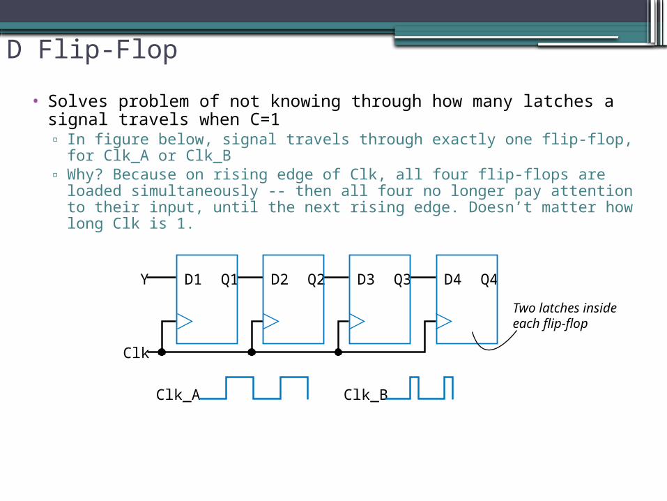
D1 Q1 D2 Q2 D3 Q3 D4
C4C3C2C1
Q4Y
Clk
Clk_A Clk_B
Clk
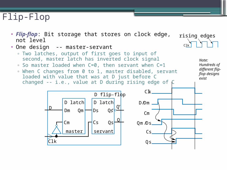
Flip-Flop
• Flip-flop: Bit storage that stores on clock edge, not level
• One design -- master-servant▫ Two latches, output of first goes to input of second,
master latch has inverted clock signal▫ So master loaded when C=0, then servant when C=1▫ When C changes from 0 to 1, master disabled, servant
loaded with value that was at D just before C changed -- i.e., value at D during rising edge of C
Clk
D/Dm
Qm/Ds
Cm
Cs
Qs
Clk
rising edges
Note: Hundreds of different flip-flop designs exist
D latch
master
D latch
servant
D Dm Ds
Cs
Qm Qs’
Qs Q
Q’
Cm
Clk
D flip-flop
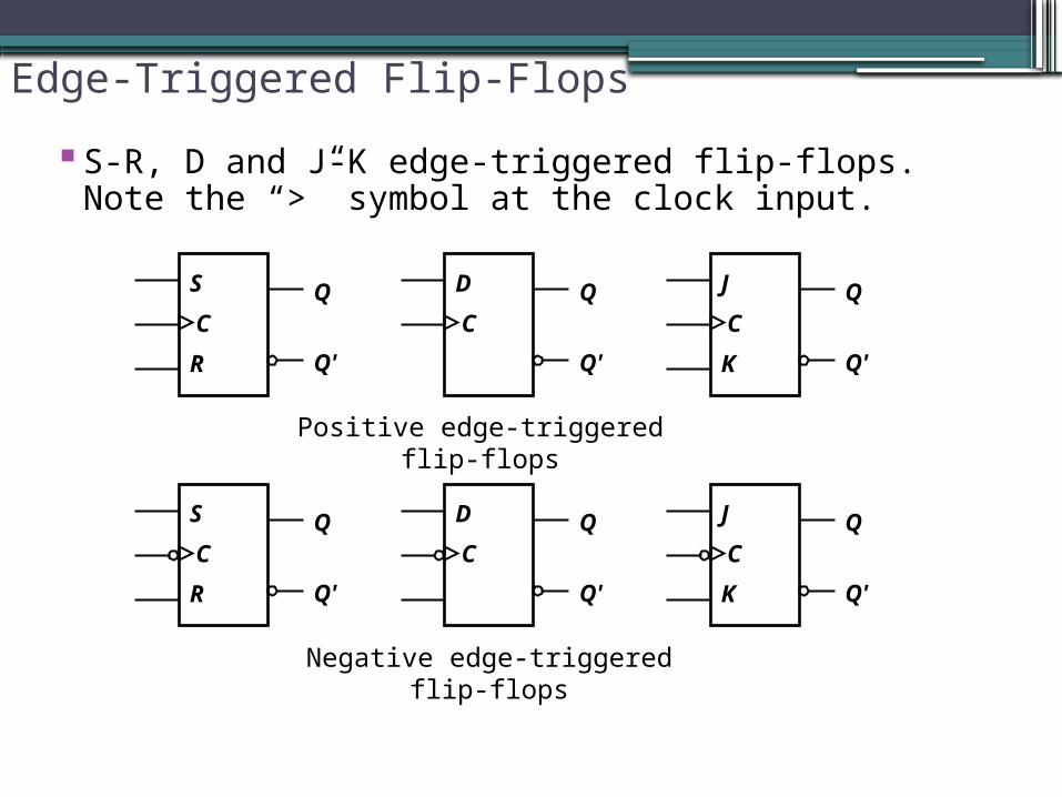
Edge-Triggered Flip-Flops
S-R, D and J-K edge-triggered flip-flops. Note the “>” symbol at the clock input.
S
C
R
Q
Q'
S
C
R
Q
Q'
D
CQ
Q'
D
CQ
Q'
J
C
K
Q
Q'
J
C
K
Q
Q'
Positive edge-triggered flip-flops
Negative edge-triggered flip-flops
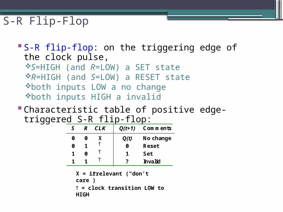
S-R Flip-Flop
S-R flip-flop: on the triggering edge of the clock pulse,S=HIGH (and R=LOW) a SET stateR=HIGH (and S=LOW) a RESET stateboth inputs LOW a no changeboth inputs HIGH a invalid
Characteristic table of positive edge-triggered S-R flip-flop:
X = irrelevant (“don’t care”)
= clock transition LOW to HIGH
S R CLK Q(t+1) Comments
0 0 X Q(t) No change
0 1 0 Reset
1 0 1 Set
1 1 ? Invalid
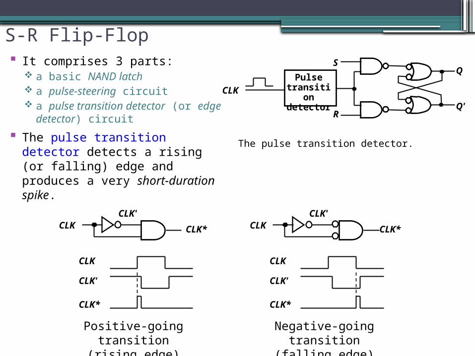
S-R Flip-Flop It comprises 3 parts:
a basic NAND latch a pulse-steering circuit a pulse transition detector (or
edge detector) circuit
The pulse transition detector detects a rising (or falling) edge and produces a very short-duration spike.
The pulse transition detector.
SQ
Q'
CLK
Pulse transition detector
R
Positive-going transition(rising edge)
CLKCLK'
CLK*
CLK'
CLK
CLK*
Negative-going transition(falling edge)
CLK'
CLK
CLK*
CLKCLK'
CLK*
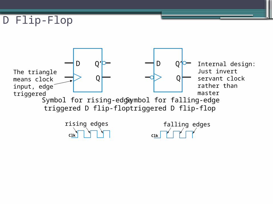
D Flip-Flop
D Q’
Q
Q’D
Q
Symbol for rising-edgetriggered D flip-flop
Symbol for falling-edgetriggered D flip-flop
Clk
rising edges
Clk
falling edges
Internal design: Just invert servant clock rather than master
The triangle means clock input, edge triggered
D Flip-Flop
• Solves problem of not knowing through how many latches a signal travels when C=1 ▫ In figure below, signal travels through exactly one flip-flop, for
Clk_A or Clk_B▫ Why? Because on rising edge of Clk, all four flip-flops are loaded
simultaneously -- then all four no longer pay attention to their input, until the next rising edge. Doesn’t matter how long Clk is 1.
D1 Q1 D2 Q2 D3 Q3 D4 Q4Y
Clk
Clk_A Clk_B
Two latches inside each flip-flop
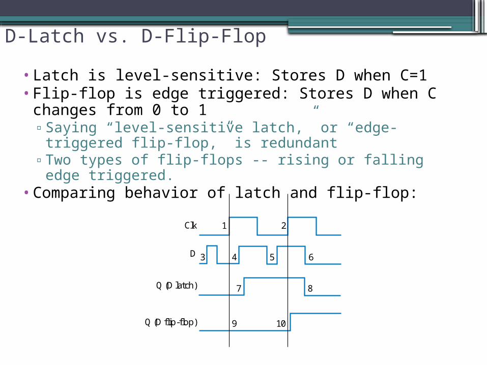
D-Latch vs. D-Flip-Flop
• Latch is level-sensitive: Stores D when C=1• Flip-flop is edge triggered: Stores D when C
changes from 0 to 1▫Saying “level-sensitive latch,” or “edge-triggered flip-
flop,” is redundant▫Two types of flip-flops -- rising or falling edge
triggered.• Comparing behavior of latch and flip-flop:
Clk
D
Q (D latch)
Q (D flip-flop) 10
87
654
9
3
1 2
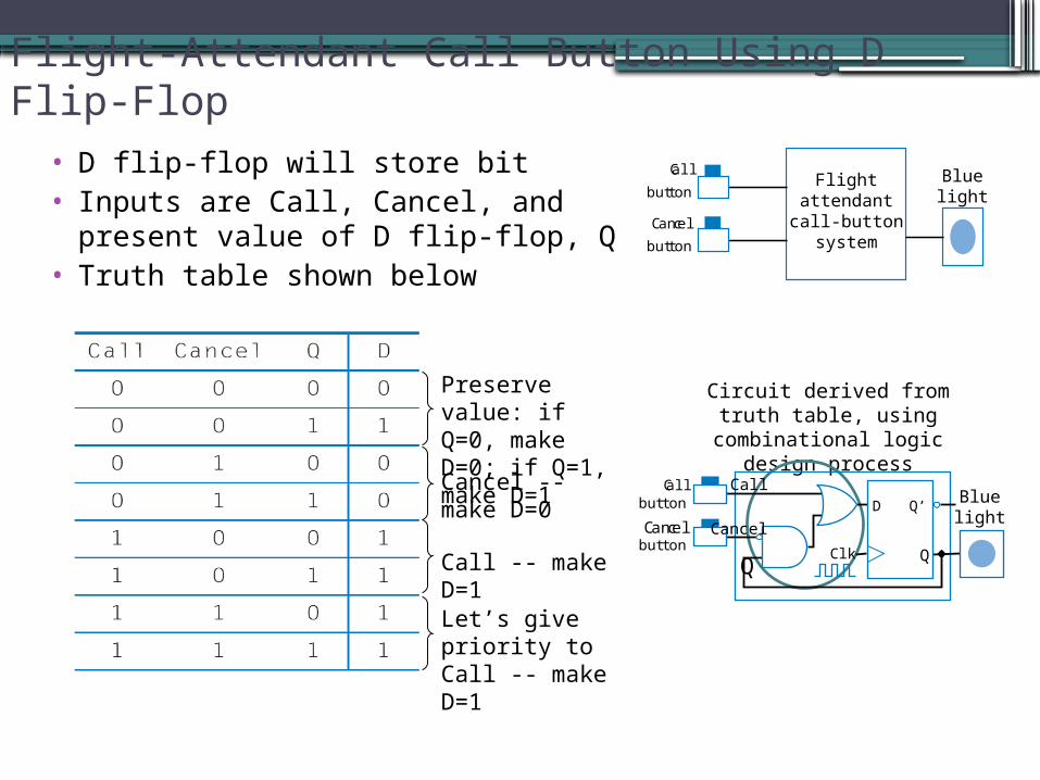
Flight-Attendant Call Button Using D Flip-Flop
• D flip-flop will store bit• Inputs are Call, Cancel, and present
value of D flip-flop, Q• Truth table shown below
Preserve value: if Q=0, make D=0; if Q=1, make D=1
Cancel -- make D=0
Call -- make D=1
Let’s give priority to Call -- make D=1
Circuit derived from truth table, using combinational logic design
process
Call
button
Cancel
button
Flightattendantcall-button
system
Bluelight
D Q’
QClk
Callbut ton
Cancelbut ton
Bluelight
Call
Cancel
Q
D Flip-Flop
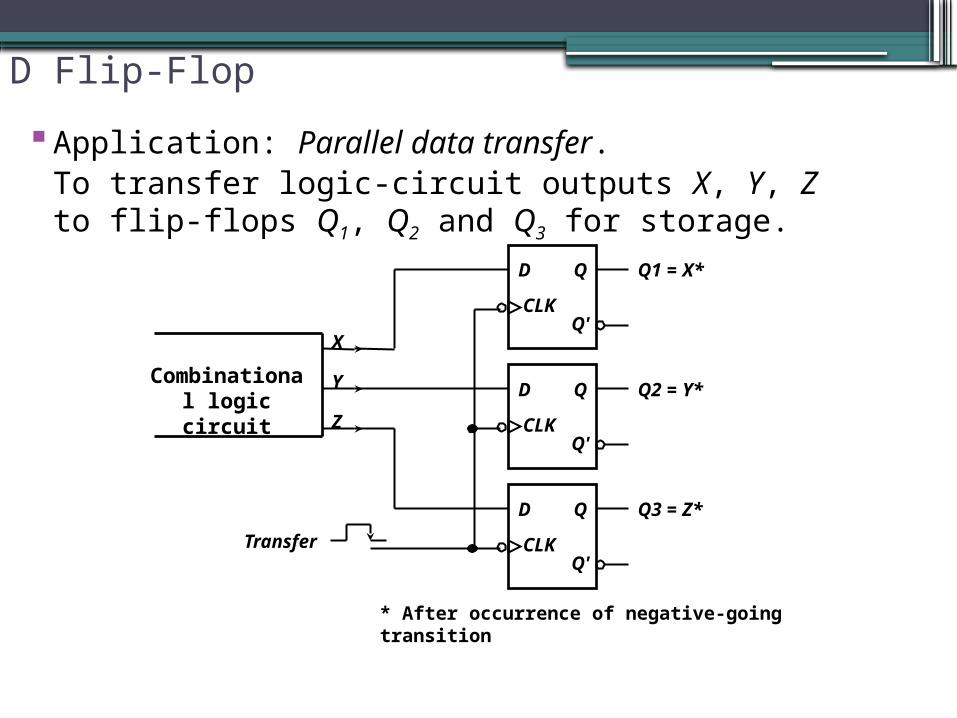
Application: Parallel data transfer.To transfer logic-circuit outputs X, Y, Z to flip-flops Q1, Q2 and Q3 for storage.
* After occurrence of negative-going transition
Q1 = X*D
CLK
Q
Q'
Q2 = Y*D
CLK
Q
Q'
Q3 = Z*D
CLK
Q
Q'
Combinational logic circuit
Transfer
X
Y
Z
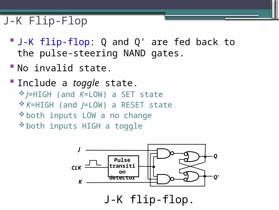
J-K Flip-Flop
J-K flip-flop: Q and Q' are fed back to the pulse-steering NAND gates.
No invalid state.
Include a toggle state. J=HIGH (and K=LOW) a SET stateK=HIGH (and J=LOW) a RESET stateboth inputs LOW a no changeboth inputs HIGH a toggle
J-K flip-flop.
JQ
Q'
CLK
Pulse transition detector
K
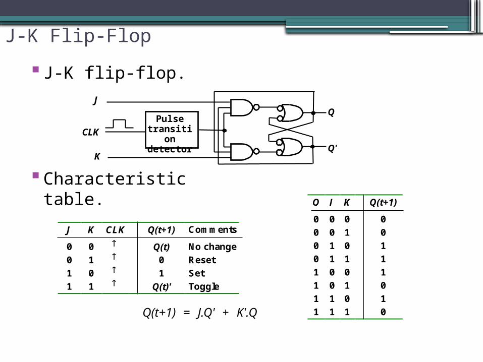
J-K Flip-Flop
J-K flip-flop.
Characteristic table.
JQ
Q'
CLK
Pulse transition detector
K
J K CLK Q(t+1) Comments
0 0 Q(t) No change
0 1 0 Reset
1 0 1 Set
1 1 Q(t)' Toggle
Q J K Q(t+1)
0 0 0 0
0 0 1 0
0 1 0 1
0 1 1 1
1 0 0 1
1 0 1 0
1 1 0 1
1 1 1 0Q(t+1) = J.Q' + K'.Q
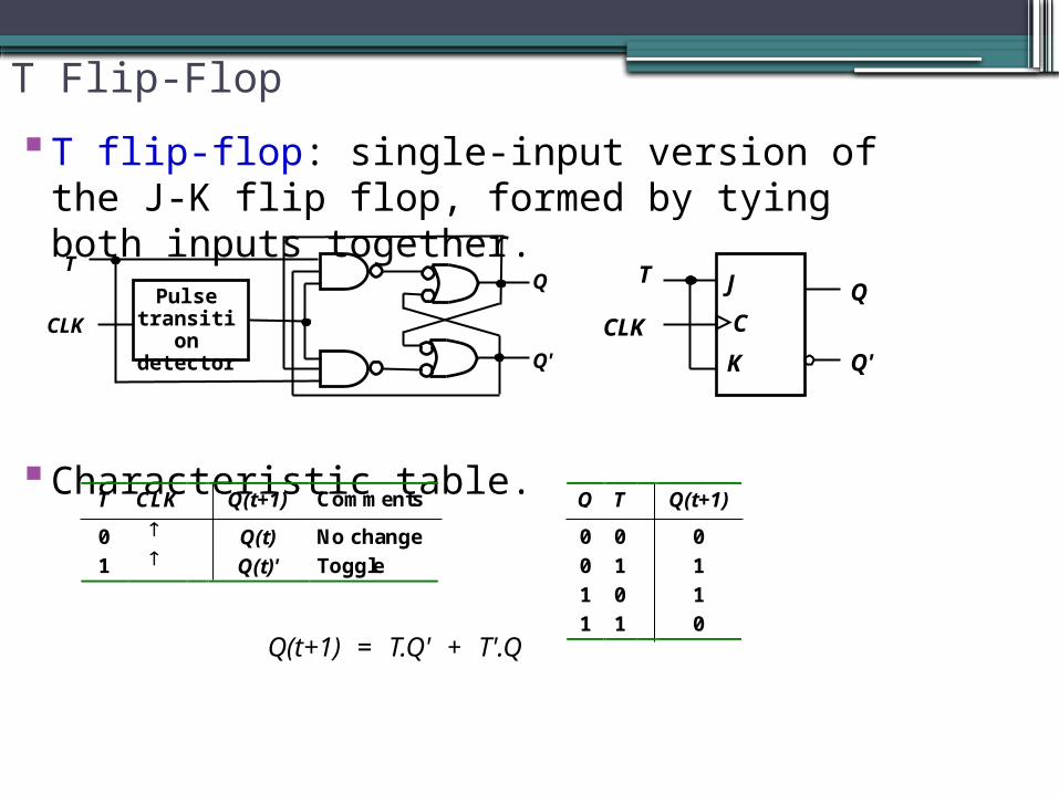
T Flip-Flop
T flip-flop: single-input version of the J-K flip flop, formed by tying both inputs together.
Characteristic table.T CLK Q(t+1) Comments
0 Q(t) No change
1 Q(t)' Toggle
Q T Q(t+1)
0 0 0
0 1 1
1 0 1
1 1 0Q(t+1) = T.Q' + T'.Q
TQ
Q'
CLK
Pulse transition detector
J
C
K
Q
Q'
CLK
T
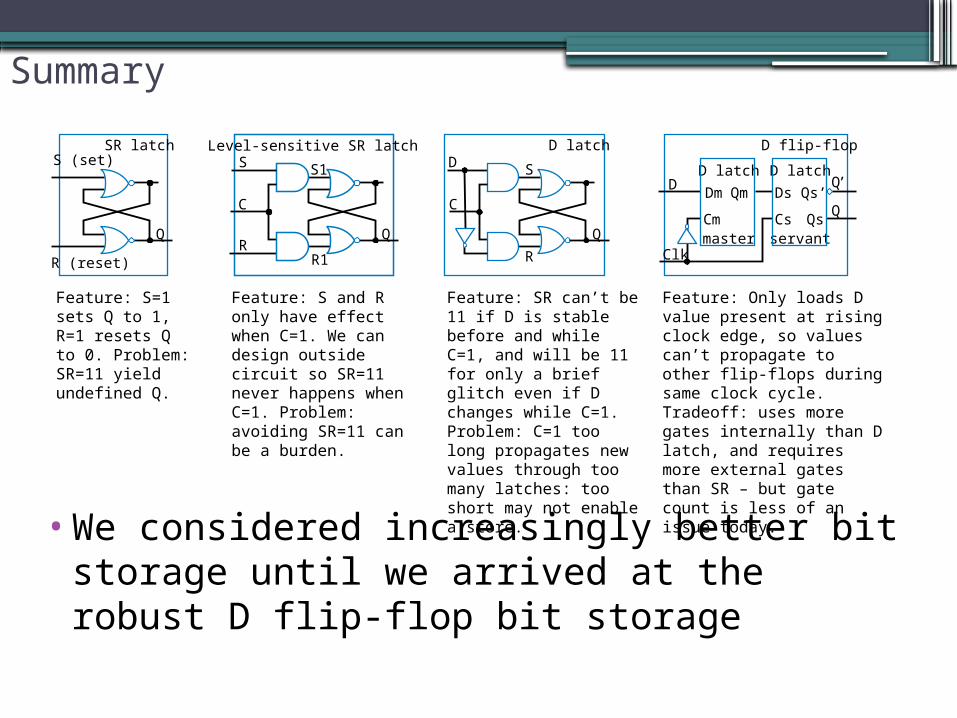
Summary
•We considered increasingly better bit storage until we arrived at the robust D flip-flop bit storage
D flip-flop
D latch
master
D latch
servant
Dm Qm
Cm
DsD
Clk
Qs’
Cs Qs
Q’
Q
S
R
D
Q
C
D latch
Feature: Only loads D value present at rising clock edge, so values can’t propagate to other flip-flops during same clock cycle. Tradeoff: uses more gates internally than D latch, and requires more external gates than SR – but gate count is less of an issue today.
Feature: SR can’t be 11 if D is stable before and while C=1, and will be 11 for only a brief glitch even if D changes while C=1. Problem: C=1 too long propagates new values through too many latches: too short may not enable a store.
Feature: S and R only have effect when C=1. We can design outside circuit so SR=11 never happens when C=1. Problem: avoiding SR=11 can be a burden.
R (reset)
S (set)
Q
SR latch
Feature: S=1 sets Q to 1, R=1 resets Q to 0. Problem: SR=11 yield undefined Q.
S1
R1
S
Q
C
R
Level-sensitive SR latch