ECE 207 Lab Project 3 Capacitor Modelrostamko/ece207/labs/Lab Week 2 -- capacitor...ECE 207 Lab...
6
ECE 207 Lab Project 3 – Capacitor Model Purpose: The measurements in this lab will determine the parallel model of a commercial capacitor. Capacitors are by no means perfect—their dielectric has an effective resistance that can be modeled as a resistance in parallel with the capacitor itself. Deliverables: Phasor data taken from the oscilloscope Calculation of the phasor current Time-domain values of the two voltages and the current Parameters of the parallel model of the capacitor Drawing of the parallel model of the capacitor Equipment: NI myDAQ, breadboard, 1-kΩ resistor, and 0.1-μF capacitor. Procedure: 1. The following test circuit serves as the basis for this lab. The left schematic is useful for analysis, and the diagram on the right shows the NI myDAQ connections: 2. Before constructing the circuit, make three measurements and record the results: a. Use the DMM to measure the resistance of the 1-k resistor, b. Measure the resistance of the capacitor, and c. Use a capacitance meter to measure C. 3. After building the capacitor test circuit, launch the NI ELVISmx Function Generator (“FGEN”) and set up the sinusoidal source for 3.5 V pp , zero DC offset, and 1000 Hz; the function generator panel should look like this:
Transcript of ECE 207 Lab Project 3 Capacitor Modelrostamko/ece207/labs/Lab Week 2 -- capacitor...ECE 207 Lab...

ECE 207 Lab Project 3 – Capacitor Model
Purpose: The measurements in this lab will determine the parallel model of a commercial capacitor. Capacitors
are by no means perfect—their dielectric has an effective resistance that can be modeled as a resistance in
parallel with the capacitor itself.
Deliverables:
Phasor data taken from the oscilloscope
Calculation of the phasor current
Time-domain values of the two voltages and the current
Parameters of the parallel model of the capacitor
Drawing of the parallel model of the capacitor
Equipment: NI myDAQ, breadboard, 1-kΩ resistor, and 0.1-µF capacitor.
Procedure:
1. The following test circuit serves as the basis for this lab. The left schematic is useful for analysis, and the
diagram on the right shows the NI myDAQ connections:
2. Before constructing the circuit, make three measurements and record the results:
a. Use the DMM to measure the resistance of the 1-k resistor,
b. Measure the resistance of the capacitor, and
c. Use a capacitance meter to measure C.
3. After building the capacitor test circuit, launch the NI ELVISmx Function Generator (“FGEN”) and set up the
sinusoidal source for 3.5 Vpp, zero DC offset, and 1000 Hz; the function generator panel should look like this:

4. Launch the NI ELVISmx Oscilloscope (“Scope”) and make the following settings:
Expect to see about five cycles with the green trace showing the function generator reference sinusoid on
Analog Input 0 (AI0) and the blue trace showing the capacitor voltage. Also observe the numerical displays
below the traces for RMS voltage, peak-to-peak voltage, and frequency. Note that you must display at least
two full cycles for these numerical displays to be accurate.
5. Record the RMS values of VS and VC.
6. Adjust the timebase setting to maximize the visible time shift between the two sinusoids. Enable the cursors
and measure “dT” with as much accuracy as possible.
7. Calculate the phase angle of VC taking VS as the reference; use phase = dT f 360 where f is the frequency
in Hz. The phase is negative if the sinusoid lags the reference, otherwise the phase is positive.
8. Form the phasor voltages VS and VC and record them on your worksheet.
9. Calculate the phasor current I using the measured value of the resistor and your two phasor voltages.
10. Transform the three phasor quantities to their time-domain equivalent representations and record them on
your worksheet. Remember that the phasors are written in RMS voltage while the time-domain
representations use peak voltage.
11. Determine C and RC for your capacitor. Treat the parallel combination of C and RC as a combined admittance
(reciprocal of impedance) whose value is YC = I / VC = 1/RC + jC.
12. Draw and label the capacitor’s parallel model.

ECE 207
Winter 2010–2011 11
Date ___________________________ Bench # __________
By ___________________________________________
___________________________________________
___________________________________________
Turn in this page with all required data, calculations,and discussion by the deadline given in the lab instructions.
Section # ______________ Lab 3
R1k = _____________________________________________
Rcapacitor = _________________________________________
Cmeasured = _________________________________________
Oscilloscope data (phasors in rms):
VS = ______________________________________________
VC = ______________________________________________
Calculated value of current (show calculation on left):
I = _______________________________________________
Time-domain values (cosines in peak values):
vS(t) = _____________________________________________
vC(t) = _____________________________________________
i(t) = ______________________________________________
Model values from YC:
C = _______________________________________________
Rc = ______________________________________________
Draw and label the R-C parallel model of the capacitor (i.e., RC and C in parallel)::
Current I calculation:
Derivation of YC and calculationof C and RC:

ECE 207 Lab Project 4 – Inductor Model
Purpose: Did the capacitor you examined in the last lab look like a capacitor? Sure, because it did exhibit
capacitance. But there was inherent resistance that looked like it was in parallel with the capacitance. The
capacitor was not very ideal.
How about inductors? After all, an inductor is a coil of wire and we should expect wire to have some resistance.
In this lab we will collect enough data to develop a model of a real inductor.
Deliverables:
Impedance of a nominal-3.3 mH inductor at a frequency of 1kHz
Resistance and inductance parameters for the series model of an inductor at 1kHz
Drawing of the circuit model
Equipment: NI myDAQ, breadboard, 1-kΩ resistor, 3.3mH inductor, and 0.01F capacitor.
Procedure:
1. The following test circuit serves as the basis for this lab. The left schematic is useful for analysis, and the
diagram on the right shows the NI myDAQ connections; the additional parallel capacitor Cp serves to reduce
high-frequency noise on the inductor voltage measurement but does not overly disturb the measurements:
2. Before constructing the circuit, make three measurements and record the results:
a. Use the DMM to measure the resistance of the 1-k resistor, and
b. Use the LCR meter (Extech 380193, also known as the “gray meter”) to measure the inductance and
resistance of the 3.3mH inductor at 1kHz; both measurements appear on the screen.
3. After building the inductor test circuit, launch the NI ELVISmx Function Generator (“FGEN”) and configure
the sinusoidal source for 3.0 Vpp, zero DC offset, and 1000 Hz.

4. Launch the NI ELVISmx Oscilloscope (“Scope”) and make the following settings:
Expect to see about five cycles with the green trace showing the inductor voltage sinusoid VL on Analog
Input 0 (AI0) and the blue trace showing the resistor voltage VR. Also observe the numerical displays below
the traces for RMS voltage, peak-to-peak voltage, and frequency. Note that you must display at least two full
cycles for these numerical displays to be accurate.
5. Record the RMS values of VL and VR.
6. Adjust the timebase setting to maximize the visible time shift between the two sinusoids. Enable the cursors
and measure “dT” with as much accuracy as possible. You will likely need to change the “Acquisition Mode”
to “Run Once” and then click the “Run” button repeatedly until you get a stable trace.
7. Calculate the phase angle of VR (blue trace) taking VL as the reference of 0 (green trace); use phase = dT f
360 where f is the frequency in Hz. The phase is negative if the sinusoid lags the reference, otherwise the
phase is positive.
8. Calculate the phasor current IL from the resistor voltage VR and the measured value of the 1-kΩ resistor.
9. Calculate the impedance of the inductor ZL = VL/IL at 1 kHz.
10. Write the impedance of the series model of the inductor. Then match real and imaginary parts to get the
values of Rs and Ls at 1kHz.
11. Draw the circuit model of the physical inductor.
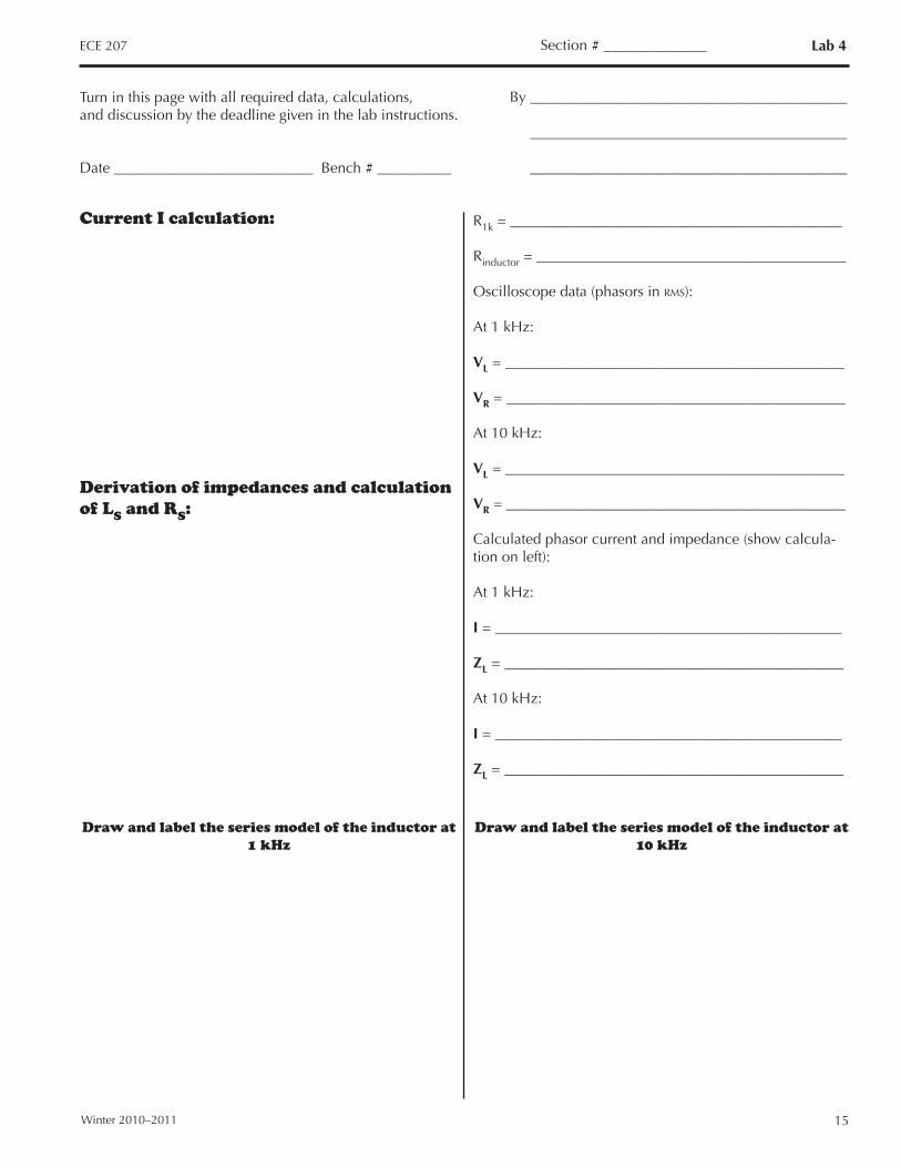
ECE 207
Winter 2010–2011 15
Date ___________________________ Bench # __________
By ___________________________________________
___________________________________________
___________________________________________
Turn in this page with all required data, calculations,and discussion by the deadline given in the lab instructions.
Section # ______________ Lab 4
R1k = _____________________________________________
Rinductor = __________________________________________
Oscilloscope data (phasors in rms):
At 1 kHz:
VL = ______________________________________________
VR = ______________________________________________
At 10 kHz:
VL = ______________________________________________
VR = ______________________________________________
Calculated phasor current and impedance (show calcula-tion on left):
At 1 kHz:
I = _______________________________________________
ZL = ______________________________________________
At 10 kHz:
I = _______________________________________________
ZL = ______________________________________________
Current I calculation:
Derivation of impedances and calculation of LS and RS:
Draw and label the series model of the inductor at 1 kHz
Draw and label the series model of the inductor at 10 kHz
doering
Rectangle
doering
Line
doering
Line
doering
Rectangle
doering
Line
doering
Line