ECC for NAND Flash - Flash Memory Summit · TexasLDPC Inc. Flash Memory Summit 2017 Santa Clara, CA...
96
ECC for NAND Flash Osso Vahabzadeh TexasLDPC Inc. Flash Memory Summit 2017 Santa Clara, CA 1
Transcript of ECC for NAND Flash - Flash Memory Summit · TexasLDPC Inc. Flash Memory Summit 2017 Santa Clara, CA...
ECC for NAND Flash
Osso Vahabzadeh
TexasLDPC Inc.
Flash Memory Summit 2017
Santa Clara, CA 1
Overview
2
• Why Is Error Correction Needed in Flash Memories?
• Error Correction Codes Fundamentals
• Low-Density Parity-Check (LDPC) Codes
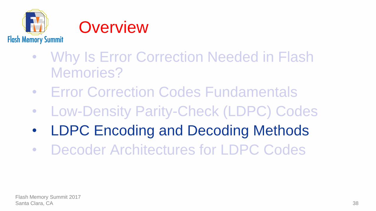
• LDPC Encoding and Decoding Methods
• Decoder Architectures for LDPC Codes
Flash Memory Summit 2017
Santa Clara, CA
Overview
3
• Why Is Error Correction Needed in Flash Memories?
• Error Correction Codes Fundamentals
• Low-Density Parity-Check (LDPC) Codes
• LDPC Encoding and Decoding Methods
• Decoder Architectures for LDPC Codes
Flash Memory Summit 2017
Santa Clara, CA
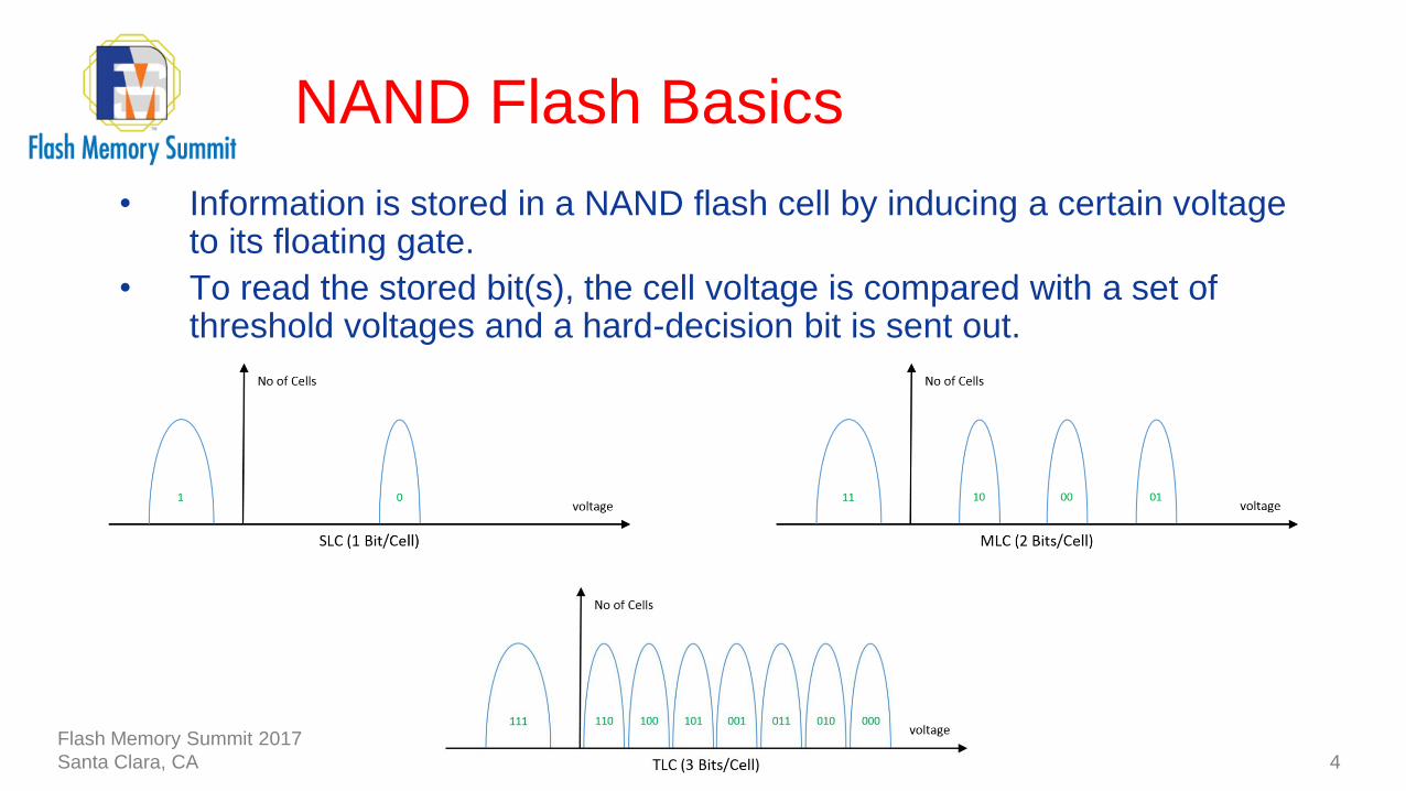
NAND Flash Basics
4
• Information is stored in a NAND flash cell by inducing a certain voltage to its floating gate.
• To read the stored bit(s), the cell voltage is compared with a set of threshold voltages and a hard-decision bit is sent out.
Flash Memory Summit 2017
Santa Clara, CA

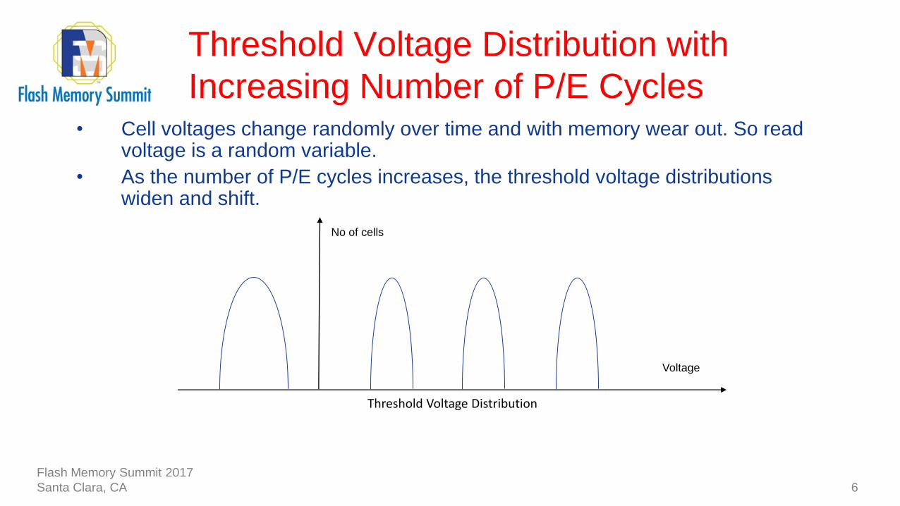
• Cell voltages change randomly over time and with memory wear out. So read voltage is a random variable.
• As the number of P/E cycles increases, the threshold voltage distributions widen and shift.
Threshold Voltage Distribution with
Increasing Number of P/E Cycles
5
Flash Memory Summit 2017
Santa Clara, CA
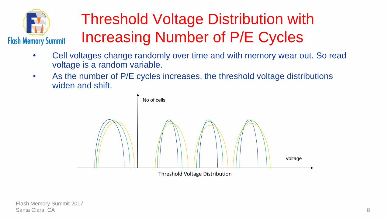
• Cell voltages change randomly over time and with memory wear out. So read voltage is a random variable.
• As the number of P/E cycles increases, the threshold voltage distributions widen and shift.
Threshold Voltage Distribution with
Increasing Number of P/E Cycles
6
Threshold Voltage Distribution
Voltage
No of cells
Flash Memory Summit 2017
Santa Clara, CA

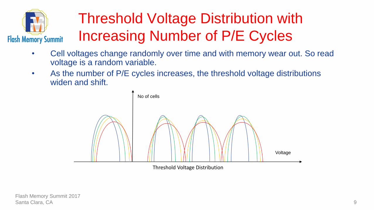
• Cell voltages change randomly over time and with memory wear out. So read voltage is a random variable.
• As the number of P/E cycles increases, the threshold voltage distributions widen and shift.
Threshold Voltage Distribution with
Increasing Number of P/E Cycles
7
Threshold Voltage Distribution
Voltage
No of cells
Flash Memory Summit 2017
Santa Clara, CA
• Cell voltages change randomly over time and with memory wear out. So read voltage is a random variable.
• As the number of P/E cycles increases, the threshold voltage distributions widen and shift.
Threshold Voltage Distribution with
Increasing Number of P/E Cycles
8
Threshold Voltage Distribution
Voltage
No of cells
Flash Memory Summit 2017
Santa Clara, CA
• Cell voltages change randomly over time and with memory wear out. So read voltage is a random variable.
• As the number of P/E cycles increases, the threshold voltage distributions widen and shift.
Threshold Voltage Distribution with
Increasing Number of P/E Cycles
9
Threshold Voltage Distribution
Voltage
No of cells
Flash Memory Summit 2017
Santa Clara, CA

• Cell voltages change randomly over time and with memory wear out. So read voltage is a random variable.
• As the number of P/E cycles increases, the threshold voltage distributions widen and shift.
Threshold Voltage Distribution with
Increasing Number of P/E Cycles
10
Threshold Voltage Distribution
Voltage
No of cells
Flash Memory Summit 2017
Santa Clara, CA
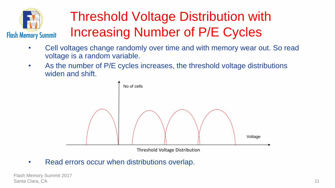
• Cell voltages change randomly over time and with memory wear out. So read voltage is a random variable.
• As the number of P/E cycles increases, the threshold voltage distributions widen and shift.
• Read errors occur when distributions overlap.
Threshold Voltage Distribution with
Increasing Number of P/E Cycles
11
Threshold Voltage Distribution
Voltage
No of cells
Flash Memory Summit 2017
Santa Clara, CA
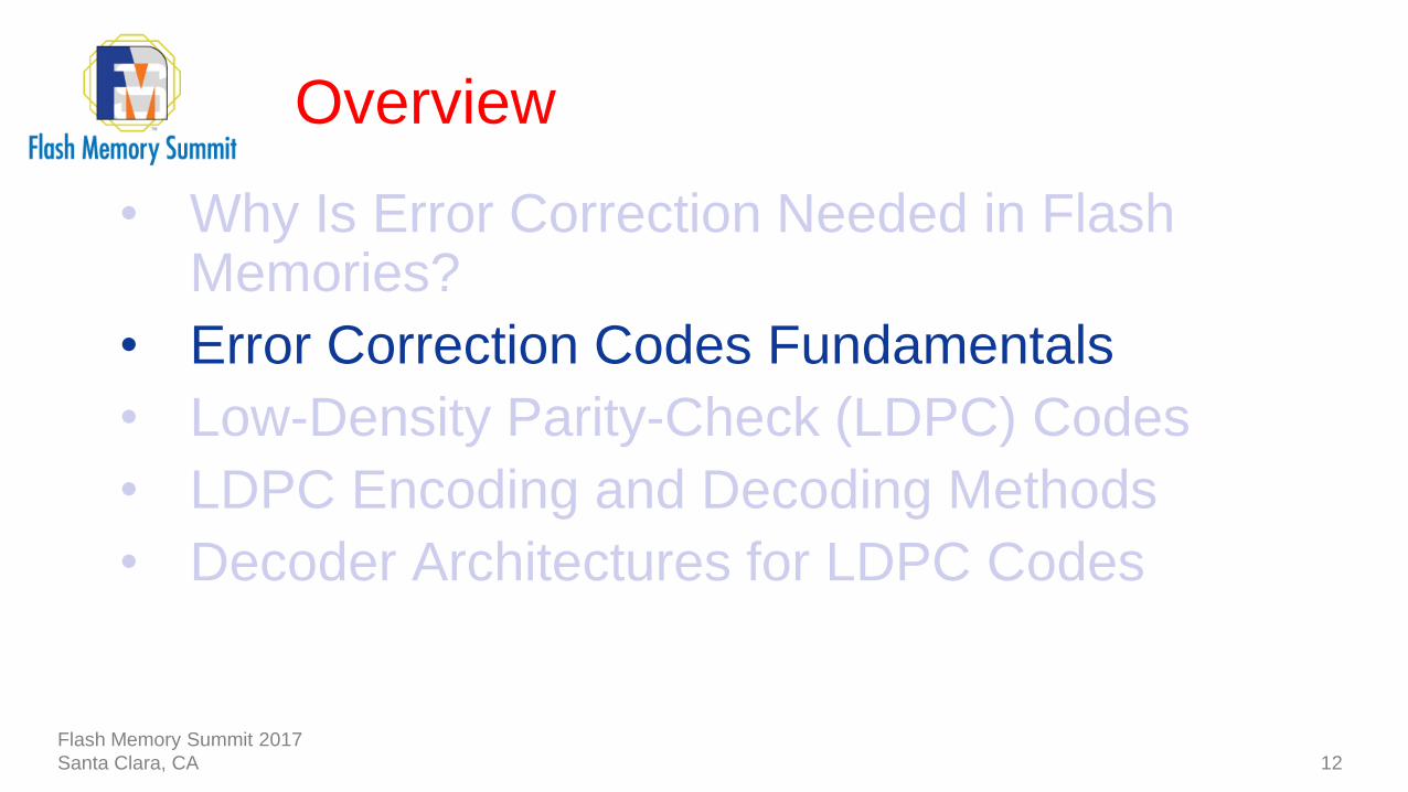
Overview
12
• Why Is Error Correction Needed in Flash Memories?
• Error Correction Codes Fundamentals
• Low-Density Parity-Check (LDPC) Codes
• LDPC Encoding and Decoding Methods
• Decoder Architectures for LDPC Codes
Flash Memory Summit 2017
Santa Clara, CA

Error Correction Codes
13
Flash Memory Summit 2017
Santa Clara, CA

Error Correction Codes
14
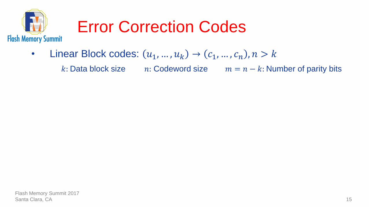
• Linear Block codes: 𝑢1, … , 𝑢𝑘 → 𝑐1, … , 𝑐𝑛 , 𝑛 > 𝑘
Flash Memory Summit 2017
Santa Clara, CA
Error Correction Codes
15
• Linear Block codes: 𝑢1, … , 𝑢𝑘 → 𝑐1, … , 𝑐𝑛 , 𝑛 > 𝑘
𝑘: Data block size 𝑛: Codeword size 𝑚 = 𝑛 − 𝑘: Number of parity bits
Flash Memory Summit 2017
Santa Clara, CA

Error Correction Codes
16
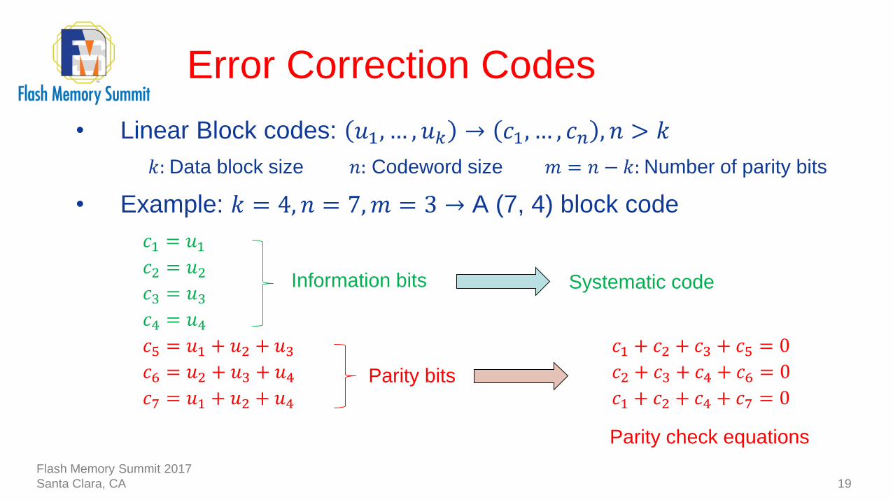
• Linear Block codes: 𝑢1, … , 𝑢𝑘 → 𝑐1, … , 𝑐𝑛 , 𝑛 > 𝑘
𝑘: Data block size 𝑛: Codeword size 𝑚 = 𝑛 − 𝑘: Number of parity bits
• Example: 𝑘 = 4, 𝑛 = 7,𝑚 = 3 → A (7, 4) block code
Flash Memory Summit 2017
Santa Clara, CA

Error Correction Codes
17
• Linear Block codes: 𝑢1, … , 𝑢𝑘 → 𝑐1, … , 𝑐𝑛 , 𝑛 > 𝑘
𝑘: Data block size 𝑛: Codeword size 𝑚 = 𝑛 − 𝑘: Number of parity bits
• Example: 𝑘 = 4, 𝑛 = 7,𝑚 = 3 → A (7, 4) block code
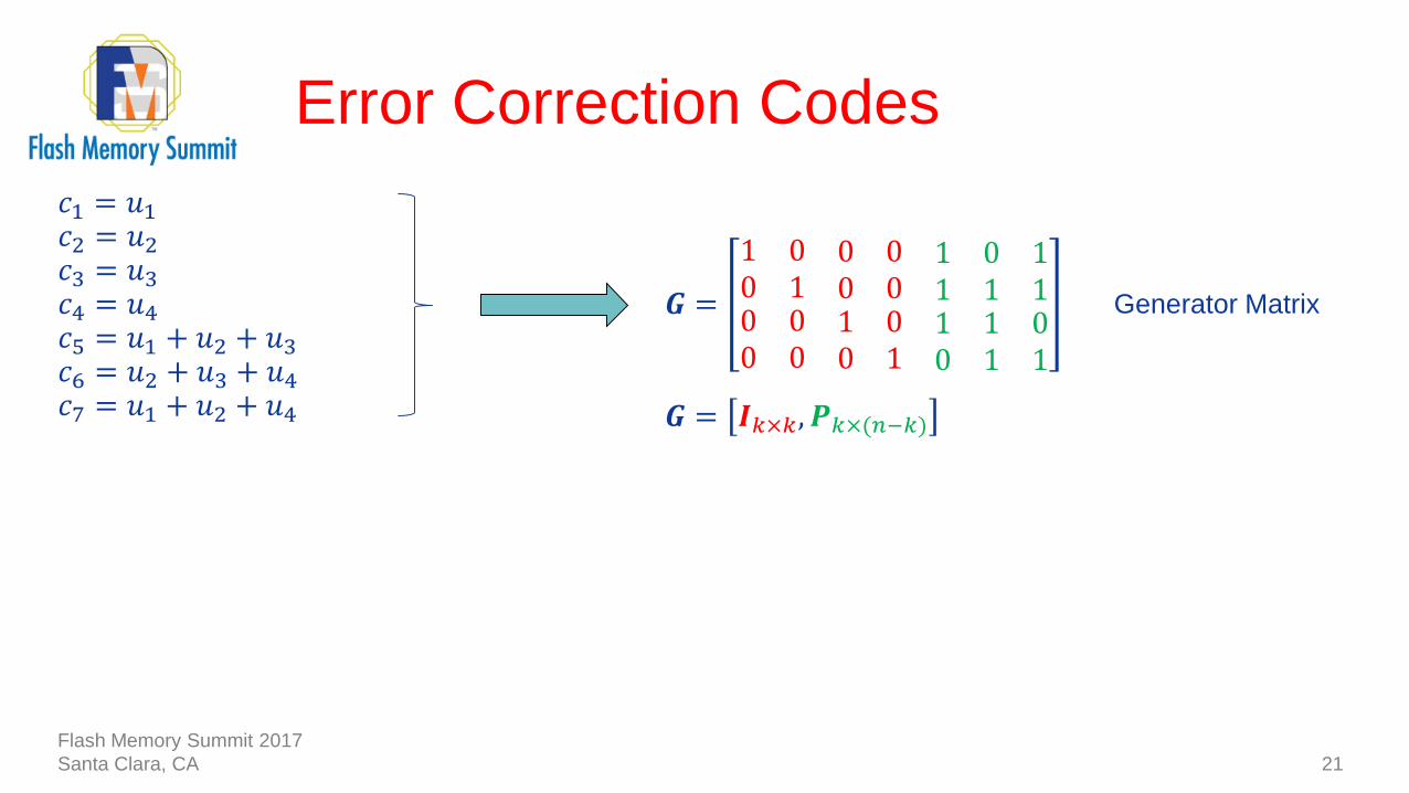
𝑐1 = 𝑢1𝑐2 = 𝑢2𝑐3 = 𝑢3𝑐4 = 𝑢4𝑐5 = 𝑢1 + 𝑢2 + 𝑢3𝑐6 = 𝑢2 + 𝑢3 + 𝑢4𝑐7 = 𝑢1 + 𝑢2 + 𝑢4
Flash Memory Summit 2017
Santa Clara, CA

Error Correction Codes
18
• Linear Block codes: 𝑢1, … , 𝑢𝑘 → 𝑐1, … , 𝑐𝑛 , 𝑛 > 𝑘
𝑘: Data block size 𝑛: Codeword size 𝑚 = 𝑛 − 𝑘: Number of parity bits
• Example: 𝑘 = 4, 𝑛 = 7,𝑚 = 3 → A (7, 4) block code
𝑐1 = 𝑢1𝑐2 = 𝑢2𝑐3 = 𝑢3𝑐4 = 𝑢4𝑐5 = 𝑢1 + 𝑢2 + 𝑢3𝑐6 = 𝑢2 + 𝑢3 + 𝑢4𝑐7 = 𝑢1 + 𝑢2 + 𝑢4
Information bits Systematic code
Flash Memory Summit 2017
Santa Clara, CA
Error Correction Codes
19
• Linear Block codes: 𝑢1, … , 𝑢𝑘 → 𝑐1, … , 𝑐𝑛 , 𝑛 > 𝑘
𝑘: Data block size 𝑛: Codeword size 𝑚 = 𝑛 − 𝑘: Number of parity bits
• Example: 𝑘 = 4, 𝑛 = 7,𝑚 = 3 → A (7, 4) block code
𝑐1 = 𝑢1𝑐2 = 𝑢2𝑐3 = 𝑢3𝑐4 = 𝑢4𝑐5 = 𝑢1 + 𝑢2 + 𝑢3 𝑐1 + 𝑐2 + 𝑐3 + 𝑐5 = 0
𝑐6 = 𝑢2 + 𝑢3 + 𝑢4 𝑐2 + 𝑐3 + 𝑐4 + 𝑐6 = 0
𝑐7 = 𝑢1 + 𝑢2 + 𝑢4 𝑐1 + 𝑐2 + 𝑐4 + 𝑐7 = 0
Information bits Systematic code
Parity bits
Parity check equations
Flash Memory Summit 2017
Santa Clara, CA
Error Correction Codes
20
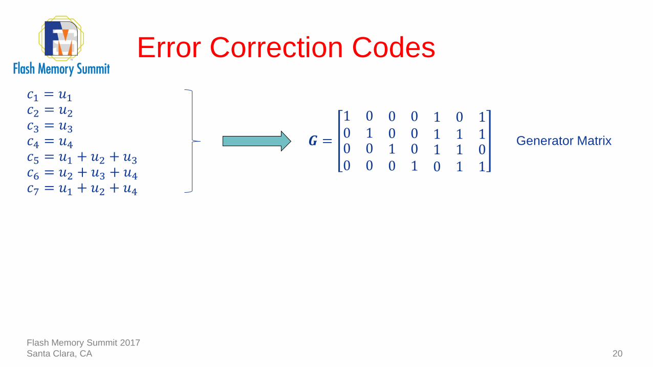
𝑐1 = 𝑢1𝑐2 = 𝑢2𝑐3 = 𝑢3𝑐4 = 𝑢4𝑐5 = 𝑢1 + 𝑢2 + 𝑢3𝑐6 = 𝑢2 + 𝑢3 + 𝑢4𝑐7 = 𝑢1 + 𝑢2 + 𝑢4
𝑮 =
1 0 0 0 1 0 10 1 0 0 1 1 10 0 1 0 1 1 00 0 0 1 0 1 1
Generator Matrix
Flash Memory Summit 2017
Santa Clara, CA
Error Correction Codes
21
𝑐1 = 𝑢1𝑐2 = 𝑢2𝑐3 = 𝑢3𝑐4 = 𝑢4𝑐5 = 𝑢1 + 𝑢2 + 𝑢3𝑐6 = 𝑢2 + 𝑢3 + 𝑢4𝑐7 = 𝑢1 + 𝑢2 + 𝑢4
𝑮 =
1 0 0 0 1 0 10 1 0 0 1 1 10 0 1 0 1 1 00 0 0 1 0 1 1
Generator Matrix
𝑮 = 𝑰𝑘×𝑘, 𝑷𝑘×(𝑛−𝑘)
Flash Memory Summit 2017
Santa Clara, CA

Error Correction Codes
22
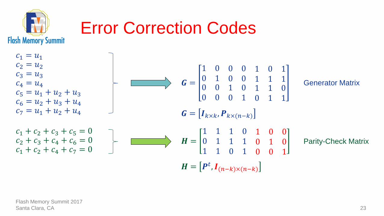
𝑐1 = 𝑢1𝑐2 = 𝑢2𝑐3 = 𝑢3𝑐4 = 𝑢4𝑐5 = 𝑢1 + 𝑢2 + 𝑢3𝑐6 = 𝑢2 + 𝑢3 + 𝑢4𝑐7 = 𝑢1 + 𝑢2 + 𝑢4
𝑐1 + 𝑐2 + 𝑐3 + 𝑐5 = 0𝑐2 + 𝑐3 + 𝑐4 + 𝑐6 = 0𝑐1 + 𝑐2 + 𝑐4 + 𝑐7 = 0
𝑮 =
1 0 0 0 1 0 10 1 0 0 1 1 10 0 1 0 1 1 00 0 0 1 0 1 1
Generator Matrix
𝑯 =1 1 1 0 1 0 00 1 1 1 0 1 01 1 0 1 0 0 1
Parity-Check Matrix
𝑮 = 𝑰𝑘×𝑘, 𝑷𝑘×(𝑛−𝑘)
Flash Memory Summit 2017
Santa Clara, CA
Error Correction Codes
23
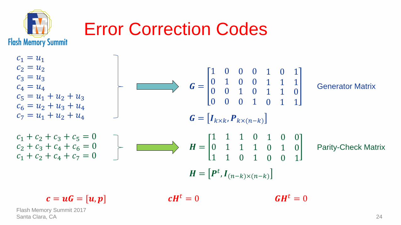
𝑐1 = 𝑢1𝑐2 = 𝑢2𝑐3 = 𝑢3𝑐4 = 𝑢4𝑐5 = 𝑢1 + 𝑢2 + 𝑢3𝑐6 = 𝑢2 + 𝑢3 + 𝑢4𝑐7 = 𝑢1 + 𝑢2 + 𝑢4
𝑐1 + 𝑐2 + 𝑐3 + 𝑐5 = 0𝑐2 + 𝑐3 + 𝑐4 + 𝑐6 = 0𝑐1 + 𝑐2 + 𝑐4 + 𝑐7 = 0
𝑮 =
1 0 0 0 1 0 10 1 0 0 1 1 10 0 1 0 1 1 00 0 0 1 0 1 1
Generator Matrix
𝑯 =1 1 1 0 1 0 00 1 1 1 0 1 01 1 0 1 0 0 1
Parity-Check Matrix
𝑮 = 𝑰𝑘×𝑘, 𝑷𝑘×(𝑛−𝑘)
𝑯 = 𝑷𝑡, 𝑰(𝑛−𝑘)×(𝑛−𝑘)
Flash Memory Summit 2017
Santa Clara, CA
Error Correction Codes
24
𝑐1 = 𝑢1𝑐2 = 𝑢2𝑐3 = 𝑢3𝑐4 = 𝑢4𝑐5 = 𝑢1 + 𝑢2 + 𝑢3𝑐6 = 𝑢2 + 𝑢3 + 𝑢4𝑐7 = 𝑢1 + 𝑢2 + 𝑢4
𝑐1 + 𝑐2 + 𝑐3 + 𝑐5 = 0𝑐2 + 𝑐3 + 𝑐4 + 𝑐6 = 0𝑐1 + 𝑐2 + 𝑐4 + 𝑐7 = 0
𝑮 =
1 0 0 0 1 0 10 1 0 0 1 1 10 0 1 0 1 1 00 0 0 1 0 1 1
Generator Matrix
𝑯 =1 1 1 0 1 0 00 1 1 1 0 1 01 1 0 1 0 0 1
Parity-Check Matrix
𝒄 = 𝒖𝑮 = [𝒖, 𝒑] 𝒄𝑯𝑡 = 0 𝑮𝑯𝑡 = 0
𝑮 = 𝑰𝑘×𝑘, 𝑷𝑘×(𝑛−𝑘)
𝑯 = 𝑷𝑡, 𝑰(𝑛−𝑘)×(𝑛−𝑘)
Flash Memory Summit 2017
Santa Clara, CA
Overview
25
• Why Is Error Correction Needed in Flash Memories?
• Error Correction Codes Fundamentals
• Low-Density Parity-Check (LDPC) Codes
• LDPC Encoding and Decoding Methods
• Decoder Architectures for LDPC Codes
Flash Memory Summit 2017
Santa Clara, CA
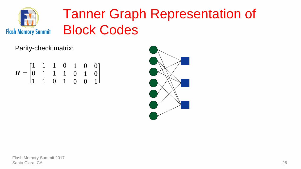
Tanner Graph Representation of
Block Codes
26
Parity-check matrix:
𝑯 =1 1 1 0 1 0 00 1 1 1 0 1 01 1 0 1 0 0 1
Flash Memory Summit 2017
Santa Clara, CA

Tanner Graph Representation of
Block Codes
27
Parity-check matrix:
𝑣7
𝑣6
𝑣5
𝑣4
𝑣3
𝑣2
𝑣1
𝑯 =1 1 1 0 1 0 00 1 1 1 0 1 01 1 0 1 0 0 1
Variable nodes: Left nodes
Flash Memory Summit 2017
Santa Clara, CA

Tanner Graph Representation of
Block Codes
Flash Memory Summit 2017
Santa Clara, CA 28
Parity-check matrix:
𝑣7
𝑣6
𝑣5
𝑣4
𝑣3
𝑣2
𝑣1
𝑐1 : 𝑣1 + 𝑣2 + 𝑣3 + 𝑣5 = 0
𝑐2 : 𝑣2 + 𝑣3 + 𝑣4 + 𝑣6 = 0
𝑐3 : 𝑣1 + 𝑣2 + 𝑣4 + 𝑣7 = 0
𝑯 =1 1 1 0 1 0 00 1 1 1 0 1 01 1 0 1 0 0 1
Variable nodes: Left nodes
Check nodes: Right nodes

Tanner Graph Representation of
Block Codes
29
Parity-check matrix:
𝑣7
𝑣6
𝑣5
𝑣4
𝑣3
𝑣2
𝑣1
𝑐1 : 𝑣1 + 𝑣2 + 𝑣3 + 𝑣5 = 0
𝑐2 : 𝑣2 + 𝑣3 + 𝑣4 + 𝑣6 = 0
𝑐3 : 𝑣1 + 𝑣2 + 𝑣4 + 𝑣7 = 0
𝑯 =1 1 1 0 1 0 00 1 1 1 0 1 01 1 0 1 0 0 1
Variable nodes: Left nodes
Check nodes: Right nodes
Edges connect variable
nodes and check nodes
Flash Memory Summit 2017
Santa Clara, CA
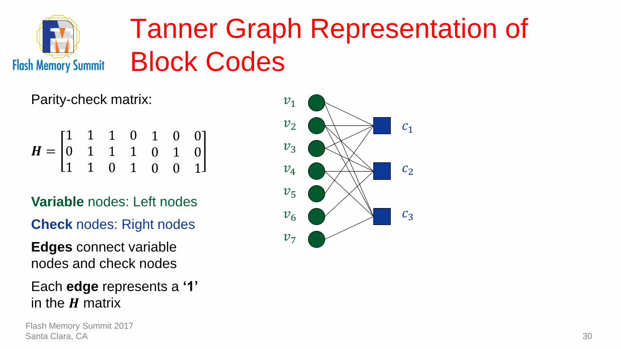
Tanner Graph Representation of
Block Codes
30
Parity-check matrix:
𝑣7
𝑣6
𝑣5
𝑣4
𝑣3
𝑣2
𝑣1
𝑐1 : 𝑣1 + 𝑣2 + 𝑣3 + 𝑣5 = 0
𝑐2 : 𝑣2 + 𝑣3 + 𝑣4 + 𝑣6 = 0
𝑐3 : 𝑣1 + 𝑣2 + 𝑣4 + 𝑣7 = 0
𝑯 =1 1 1 0 1 0 00 1 1 1 0 1 01 1 0 1 0 0 1
Variable nodes: Left nodes
Check nodes: Right nodes
Edges connect variable
nodes and check nodes
Each edge represents a ‘1’
in the 𝑯 matrix
Flash Memory Summit 2017
Santa Clara, CA
Tanner Graph Representation of
Block Codes
31
Parity-check matrix:
𝑣7
𝑣6
𝑣5
𝑣4
𝑣3
𝑣2
𝑣1
𝑐1 : 𝑣1 + 𝑣2 + 𝑣3 + 𝑣5 = 0
𝑐2 : 𝑣2 + 𝑣3 + 𝑣4 + 𝑣6 = 0
𝑐3 : 𝑣1 + 𝑣2 + 𝑣4 + 𝑣7 = 0
𝑯 =1 1 1 0 1 0 00 1 1 1 0 1 01 1 0 1 0 0 1
Variable nodes: Left nodes
Check nodes: Right nodes
Edges connect variable
nodes and check nodes
Each edge represents a ‘1’
in the 𝑯 matrix
Degree of a node is the number
of edges connected to it
Flash Memory Summit 2017
Santa Clara, CA
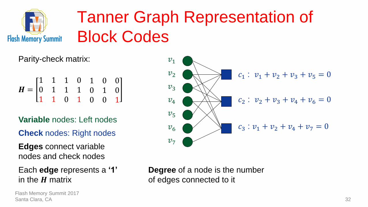
Tanner Graph Representation of
Block Codes
32
Parity-check matrix:
𝑣7
𝑣6
𝑣5
𝑣4
𝑣3
𝑣2
𝑣1
𝑐1 : 𝑣1 + 𝑣2 + 𝑣3 + 𝑣5 = 0
𝑐2 : 𝑣2 + 𝑣3 + 𝑣4 + 𝑣6 = 0
𝑐3 : 𝑣1 + 𝑣2 + 𝑣4 + 𝑣7 = 0
𝑯 =1 1 1 0 1 0 00 1 1 1 0 1 01 1 0 1 0 0 1
Variable nodes: Left nodes
Check nodes: Right nodes
Edges connect variable
nodes and check nodes
Each edge represents a ‘1’
in the 𝑯 matrix
Degree of a node is the number
of edges connected to it
Flash Memory Summit 2017
Santa Clara, CA
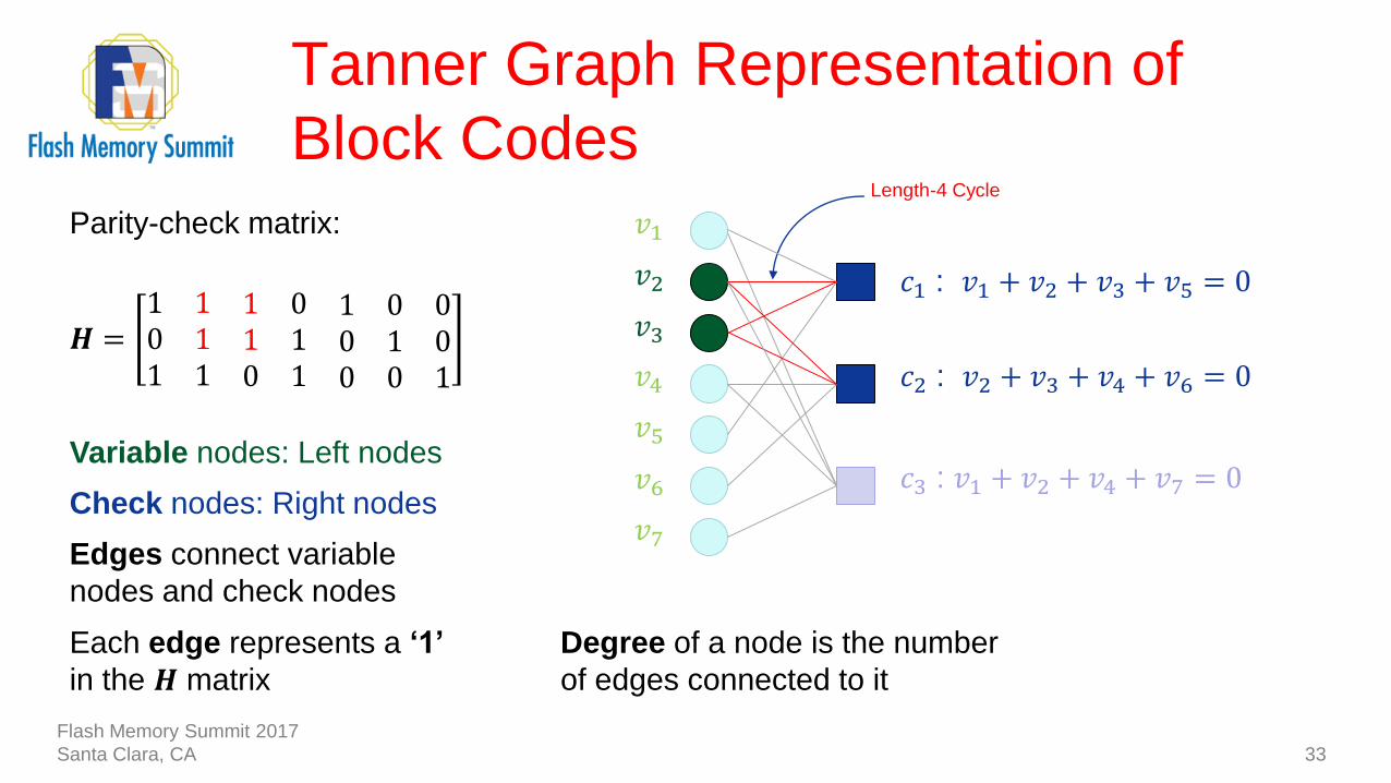
Tanner Graph Representation of
Block Codes
33
Parity-check matrix:
𝑣7
𝑣6
𝑣5
𝑣4
𝑣3
𝑣2
𝑣1
𝑯 =1 1 1 0 1 0 00 1 1 1 0 1 01 1 0 1 0 0 1
Variable nodes: Left nodes
Check nodes: Right nodes
Edges connect variable
nodes and check nodes
Each edge represents a ‘1’
in the 𝑯 matrix
Degree of a node is the number
of edges connected to it
Length-4 Cycle
𝑐1 : 𝑣1 + 𝑣2 + 𝑣3 + 𝑣5 = 0
𝑐2 : 𝑣2 + 𝑣3 + 𝑣4 + 𝑣6 = 0
𝑐3 : 𝑣1 + 𝑣2 + 𝑣4 + 𝑣7 = 0
Flash Memory Summit 2017
Santa Clara, CA
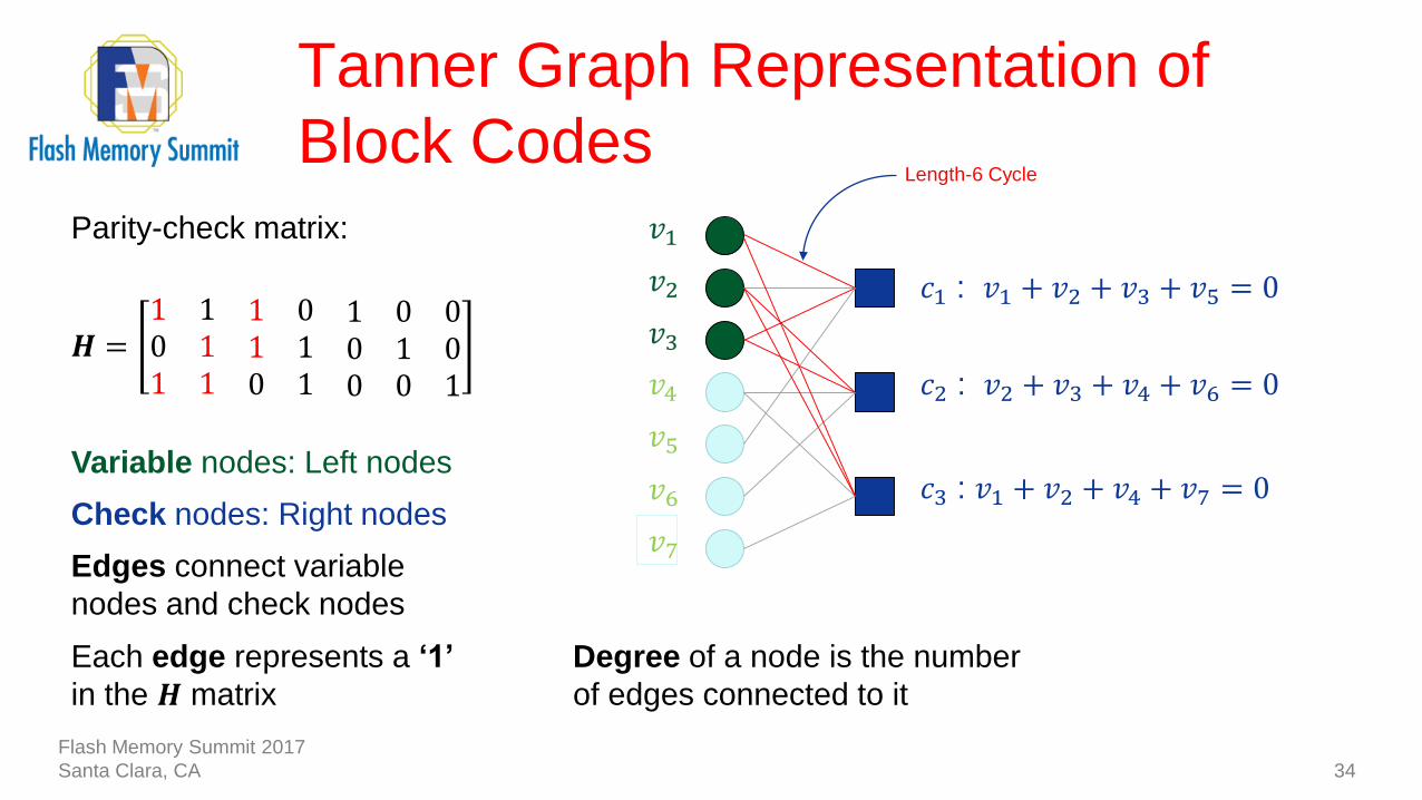
Tanner Graph Representation of
Block Codes
34
Parity-check matrix:
𝑣7
𝑣6
𝑣5
𝑣4
𝑣3
𝑣2
𝑣1
𝑯 =1 1 1 0 1 0 00 1 1 1 0 1 01 1 0 1 0 0 1
Variable nodes: Left nodes
Check nodes: Right nodes
Edges connect variable
nodes and check nodes
Each edge represents a ‘1’
in the 𝑯 matrix
Degree of a node is the number
of edges connected to it
Length-6 Cycle
𝑐1 : 𝑣1 + 𝑣2 + 𝑣3 + 𝑣5 = 0
𝑐2 : 𝑣2 + 𝑣3 + 𝑣4 + 𝑣6 = 0
𝑐3 : 𝑣1 + 𝑣2 + 𝑣4 + 𝑣7 = 0
Flash Memory Summit 2017
Santa Clara, CA
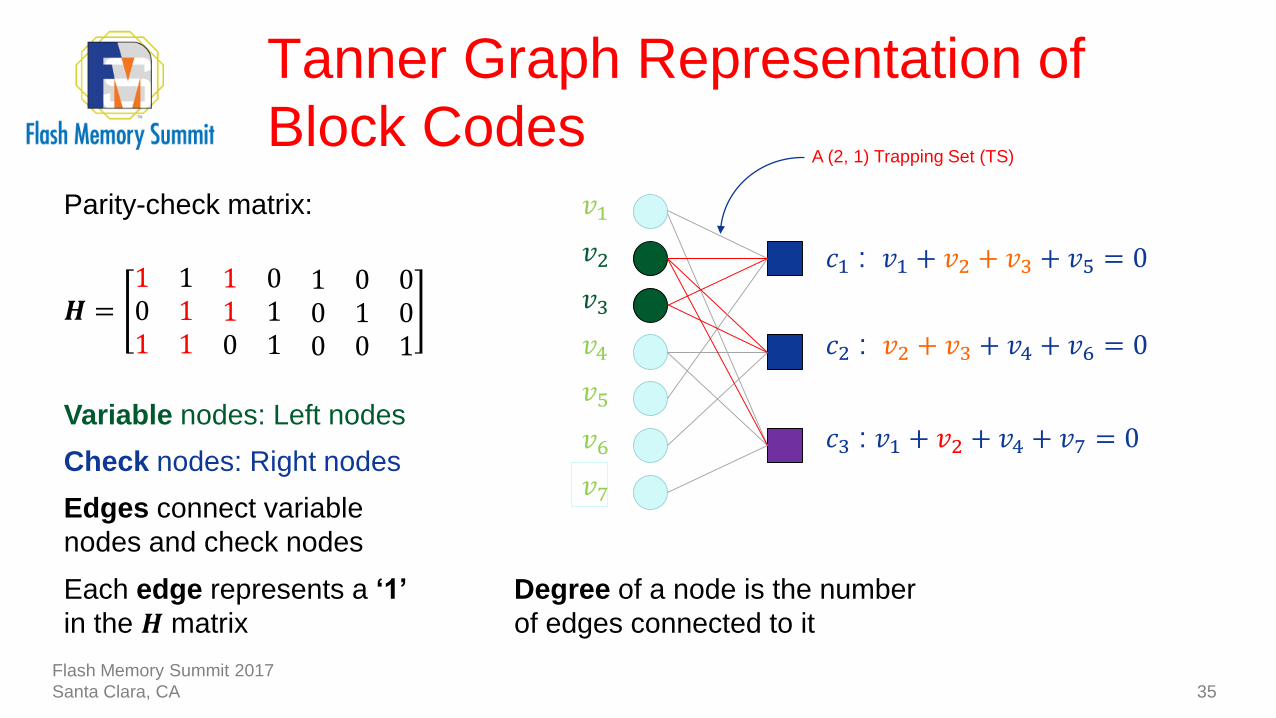
Tanner Graph Representation of
Block Codes
35
Parity-check matrix:
𝑣7
𝑣6
𝑣5
𝑣4
𝑣3
𝑣2
𝑣1
𝑯 =1 1 1 0 1 0 00 1 1 1 0 1 01 1 0 1 0 0 1
Variable nodes: Left nodes
Check nodes: Right nodes
Edges connect variable
nodes and check nodes
Each edge represents a ‘1’
in the 𝑯 matrix
Degree of a node is the number
of edges connected to it
A (2, 1) Trapping Set (TS)
𝑐1 : 𝑣1 + 𝑣2 + 𝑣3 + 𝑣5 = 0
𝑐2 : 𝑣2 + 𝑣3 + 𝑣4 + 𝑣6 = 0
𝑐3 : 𝑣1 + 𝑣2 + 𝑣4 + 𝑣7 = 0
Flash Memory Summit 2017
Santa Clara, CA
LDPC Codes
36
• Linear block codes with low-density parity-check matrices
• Number of nonzeros increases linearly with the block length (sparseness)
• Iterative message passing decoders
• Decoding complexity depends linearly on the number of nonzeros and on block length
• The generator matrix is constructed from a sparse parity-check matrix
Flash Memory Summit 2017
Santa Clara, CA

QC-LDPC Matrix: Example
37
)1)(1(2)1(1
)1(242
12
...
:
...
...
...
rccc
r
r
I
I
I
IIII
H
01....00
:
00....10
00...01
10...00
Example H Matrix: Array LDPC code
r: row/ check node degree = 5
c: column/variable node degree = 3
Sc: circulant size = 7
N: code length = Sc × r = 35
Flash Memory Summit 2017
Santa Clara, CA
Overview
38
• Why Is Error Correction Needed in Flash Memories?
• Error Correction Codes Fundamentals
• Low-Density Parity-Check (LDPC) Codes
• LDPC Encoding and Decoding Methods
• Decoder Architectures for LDPC Codes
Flash Memory Summit 2017
Santa Clara, CA
LDPC Encoding
39
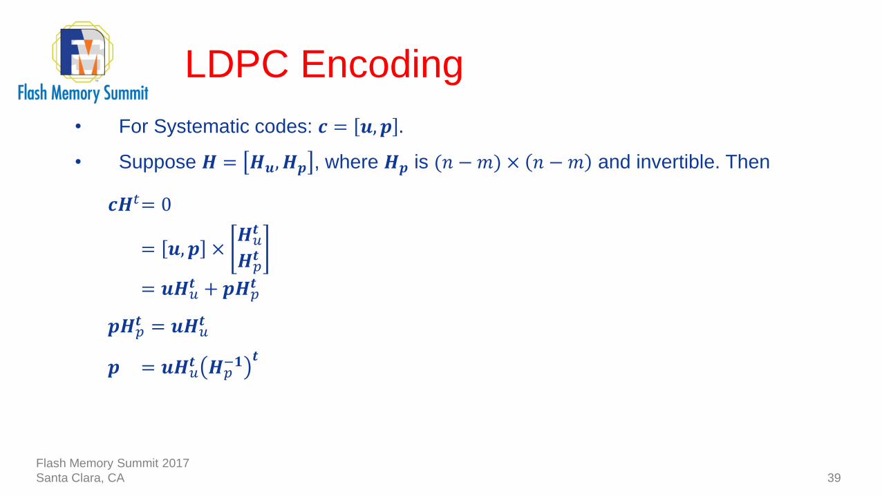
• For Systematic codes: 𝒄 = 𝒖, 𝒑 .
• Suppose 𝑯 = 𝑯𝒖, 𝑯𝒑 , where 𝑯𝒑 is (𝑛 −𝑚) × 𝑛 −𝑚 and invertible. Then
𝒄𝑯𝑡= 0
= 𝒖, 𝒑 ×𝑯𝑢𝒕
𝑯𝑝𝒕
= 𝒖𝑯𝑢𝒕 + 𝒑𝑯𝑝
𝒕
𝒑𝑯𝑝𝒕 = 𝒖𝑯𝑢
𝒕
𝒑 = 𝒖𝑯𝑢𝒕 𝑯𝑝
−𝟏 𝒕
Flash Memory Summit 2017
Santa Clara, CA

LDPC Encoding
40
• For Systematic codes: 𝒄 = 𝒖, 𝒑 .
• Suppose 𝑯 = 𝑯𝒖, 𝑯𝒑 , where 𝑯𝒑 is (𝑛 −𝑚) × 𝑛 −𝑚 and invertible. Then
𝒄𝑯𝑡= 0
= 𝒖, 𝒑 ×𝑯𝑢𝒕
𝑯𝑝𝒕
= 𝒖𝑯𝑢𝒕 + 𝒑𝑯𝑝
𝒕
𝒑𝑯𝑝𝒕 = 𝒖𝑯𝑢
𝒕
𝒑 = 𝒖𝑯𝑢𝒕 𝑯𝑝
−𝟏 𝒕
Flash Memory Summit 2017
Santa Clara, CA
LDPC Decoding
(The Bit-Flipping Algorithm), 1/2
41Flash Memory Summit 2017
Santa Clara, CA
LDPC Decoding
(The Bit-Flipping Algorithm), 1/2
42
• Bit flipping is a hard decision (HD) decoding method
Flash Memory Summit 2017
Santa Clara, CA

LDPC Decoding
(The Bit-Flipping Algorithm), 1/2
43
1
n = 1n = 0 n = 2 n = 3 n = 4 n = 5 n = 6
0 0 0000
m = 0 m = 1 m = 2
• Bit flipping is a hard decision (HD) decoding method
Flash Memory Summit 2017
Santa Clara, CA

LDPC Decoding
(The Bit-Flipping Algorithm), 1/2
Flash Memory Summit 2017
Santa Clara, CA44
1
n = 1n = 0 n = 2 n = 3 n = 4 n = 5 n = 6
0 0 0000
m = 0 m = 1 m = 2
0 + 0 + 1 = 1 0 + 1 + 0 = 1 1 + 0 + 0 = 1
• Bit flipping is a hard decision (HD) decoding method
LDPC Decoding
(The Bit-Flipping Algorithm), 1/2
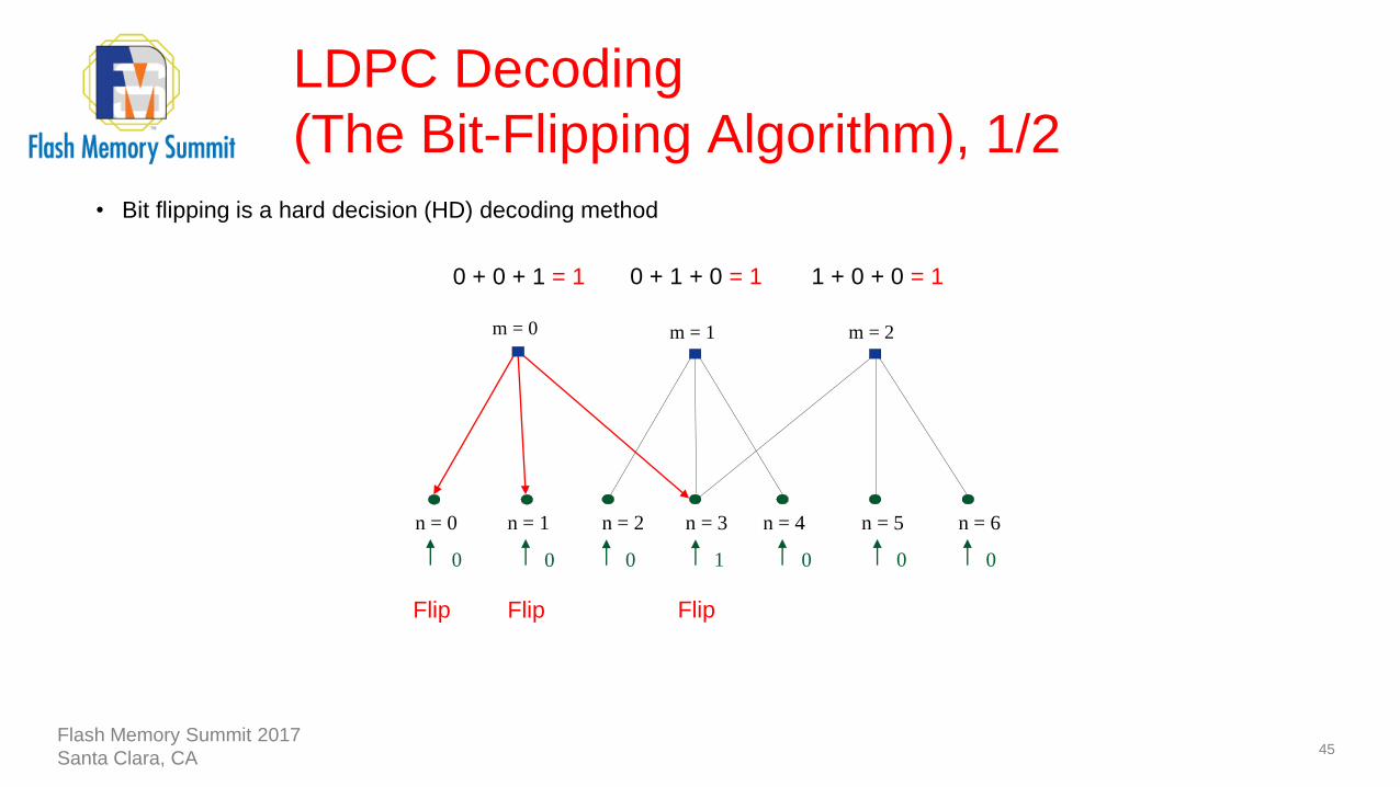
45
1
n = 1n = 0 n = 2 n = 3 n = 4 n = 5 n = 6
0 0 0000
m = 0 m = 1 m = 2
0 + 0 + 1 = 1 0 + 1 + 0 = 1 1 + 0 + 0 = 1
Flip Flip Flip
• Bit flipping is a hard decision (HD) decoding method
Flash Memory Summit 2017
Santa Clara, CA
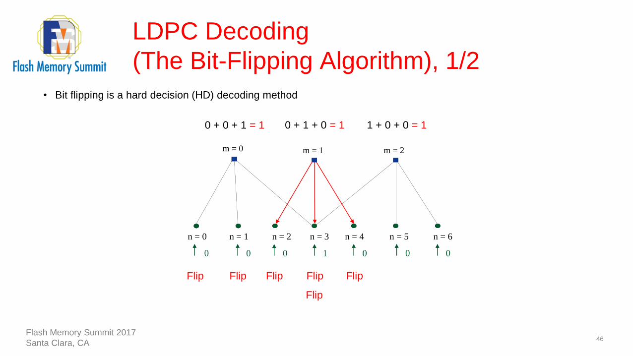
LDPC Decoding
(The Bit-Flipping Algorithm), 1/2
46
1
n = 1n = 0 n = 2 n = 3 n = 4 n = 5 n = 6
0 0 0000
m = 0 m = 1 m = 2
0 + 0 + 1 = 1 0 + 1 + 0 = 1 1 + 0 + 0 = 1
Flip Flip FlipFlip
Flip
Flip
• Bit flipping is a hard decision (HD) decoding method
Flash Memory Summit 2017
Santa Clara, CA
LDPC Decoding
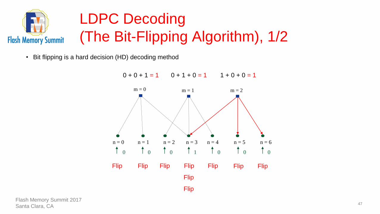
(The Bit-Flipping Algorithm), 1/2
47
1
n = 1n = 0 n = 2 n = 3 n = 4 n = 5 n = 6
0 0 0000
m = 0 m = 1 m = 2
0 + 0 + 1 = 1 0 + 1 + 0 = 1 1 + 0 + 0 = 1
Flip Flip FlipFlip
Flip
Flip Flip Flip
Flip
• Bit flipping is a hard decision (HD) decoding method
Flash Memory Summit 2017
Santa Clara, CA
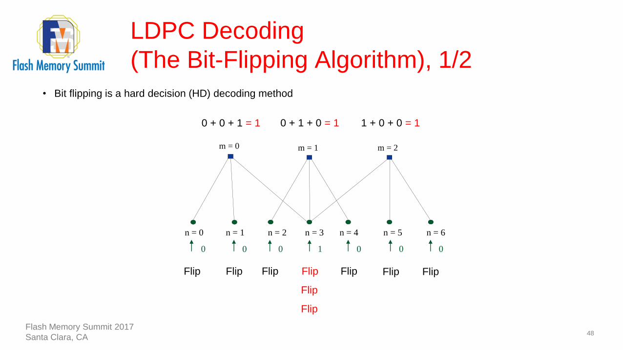
LDPC Decoding
(The Bit-Flipping Algorithm), 1/2
48
1
n = 1n = 0 n = 2 n = 3 n = 4 n = 5 n = 6
0 0 0000
m = 0 m = 1 m = 2
0 + 0 + 1 = 1 0 + 1 + 0 = 1 1 + 0 + 0 = 1
Flip Flip FlipFlip
Flip
Flip Flip Flip
Flip
• Bit flipping is a hard decision (HD) decoding method
Flash Memory Summit 2017
Santa Clara, CA

LDPC Decoding
(The Bit-Flipping Algorithm), 2/2
49
0
n = 1n = 0 n = 2 n = 3 n = 4 n = 5 n = 6
0 0 0000
m = 0 m = 1 m = 2
• Bit flipping is a hard decision (HD) decoding method
Flash Memory Summit 2017
Santa Clara, CA

LDPC Decoding
(The Bit-Flipping Algorithm), 2/2
50
0
n = 1n = 0 n = 2 n = 3 n = 4 n = 5 n = 6
0 0 0000
m = 0 m = 1 m = 2
0 + 0 + 0 = 0 0 + 0 + 0 = 0 0 + 0 + 0 = 0
• Bit flipping is a hard decision (HD) decoding method
Flash Memory Summit 2017
Santa Clara, CA
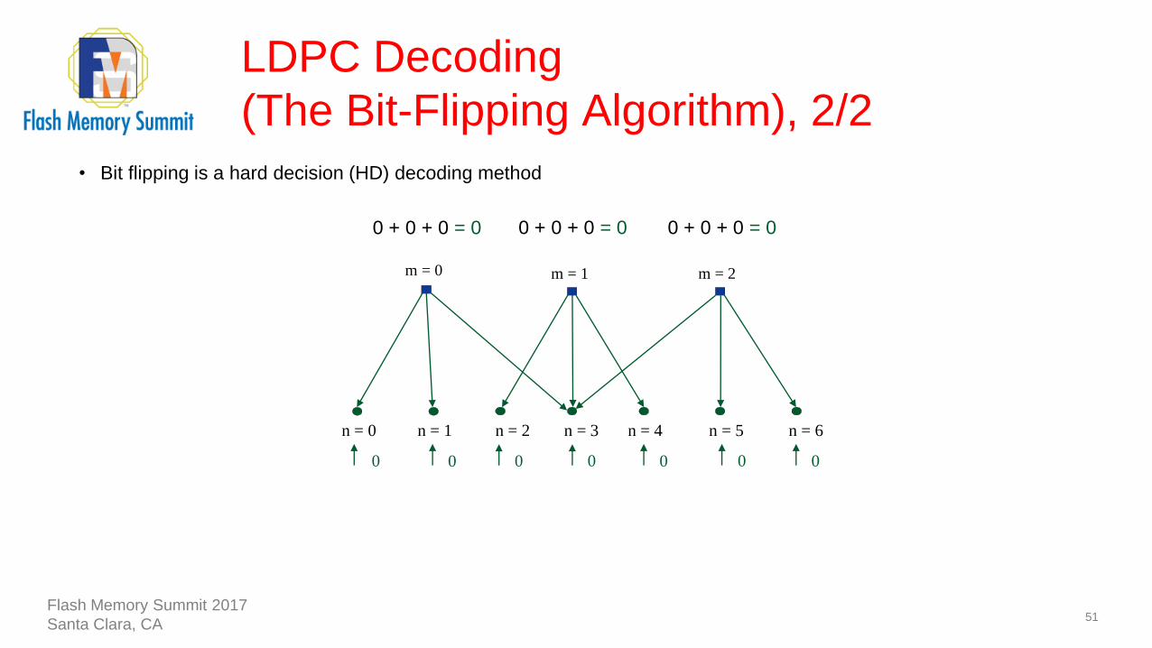
LDPC Decoding
(The Bit-Flipping Algorithm), 2/2
51
0
n = 1n = 0 n = 2 n = 3 n = 4 n = 5 n = 6
0 0 0000
m = 0 m = 1 m = 2
0 + 0 + 0 = 0 0 + 0 + 0 = 0 0 + 0 + 0 = 0
• Bit flipping is a hard decision (HD) decoding method
Flash Memory Summit 2017
Santa Clara, CA

LDPC Decoding
(The Bit-Flipping Algorithm), 2/2
52
0
n = 1n = 0 n = 2 n = 3 n = 4 n = 5 n = 6
0 0 0000
m = 0 m = 1 m = 2
0 + 0 + 0 = 0 0 + 0 + 0 = 0 0 + 0 + 0 = 0
Stay Stay StayStay
Stay
Stay Stay Stay
Stay
• Bit flipping is a hard decision (HD) decoding method
Flash Memory Summit 2017
Santa Clara, CA

Message Passing Decoding of LDPC
Codes, 1/2
53
• The decoding is successful when all the parity checks are satisfied (i.e. zero).
Flash Memory Summit 2017
Santa Clara, CA
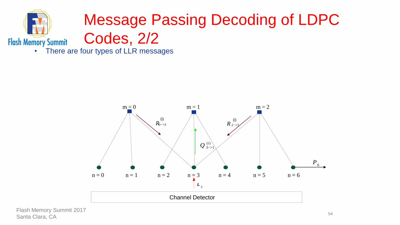
• There are four types of LLR messages
Message Passing Decoding of LDPC
Codes, 2/2
Flash Memory Summit 2017
Santa Clara, CA54
33>
(i)
0R(i)
Channel Detector
)(
13
iQ >
R
n = 1
>
m = 2m = 1m = 0
L3
2
6P
n = 0 n = 2 n = 3 n = 4 n = 5 n = 6
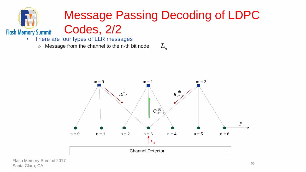
• There are four types of LLR messages
o Message from the channel to the n-th bit node,
Message Passing Decoding of LDPC
Codes, 2/2
55
nL
33>
(i)
0R(i)
Channel Detector
)(
13
iQ >
R
n = 1
>
m = 2m = 1m = 0
L3
2
6P
n = 0 n = 2 n = 3 n = 4 n = 5 n = 6
Flash Memory Summit 2017
Santa Clara, CA
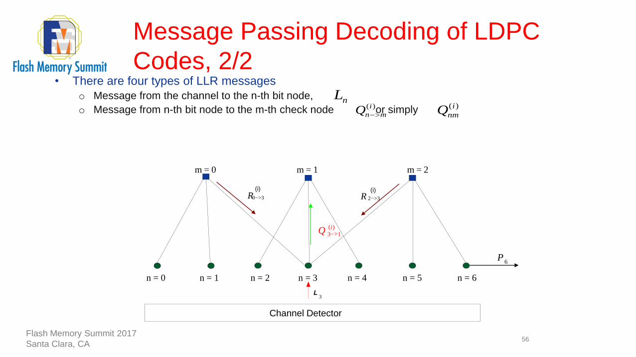
• There are four types of LLR messages
o Message from the channel to the n-th bit node,
o Message from n-th bit node to the m-th check node or simply
Message Passing Decoding of LDPC
Codes, 2/2
56
( )i
n mQ >
nL( )i
nmQ
33>
(i)
0R(i)
Channel Detector
)(
13
iQ >
R
n = 1
>
m = 2m = 1m = 0
L3
2
6P
n = 0 n = 2 n = 3 n = 4 n = 5 n = 6
Flash Memory Summit 2017
Santa Clara, CA
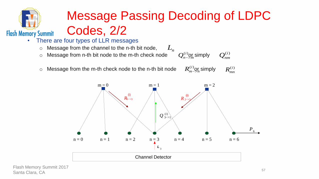
• There are four types of LLR messages
o Message from the channel to the n-th bit node,
o Message from n-th bit node to the m-th check node or simply
o Message from the m-th check node to the n-th bit node or simply
Message Passing Decoding of LDPC
Codes, 2/2
57
( )i
n mQ >
( )i
m nR >
nL( )i
nmQ
( )i
mnR
33>
(i)
0R(i)
Channel Detector
)(
13
iQ >
R
n = 1
>
m = 2m = 1m = 0
L3
2
6P
n = 0 n = 2 n = 3 n = 4 n = 5 n = 6
Flash Memory Summit 2017
Santa Clara, CA
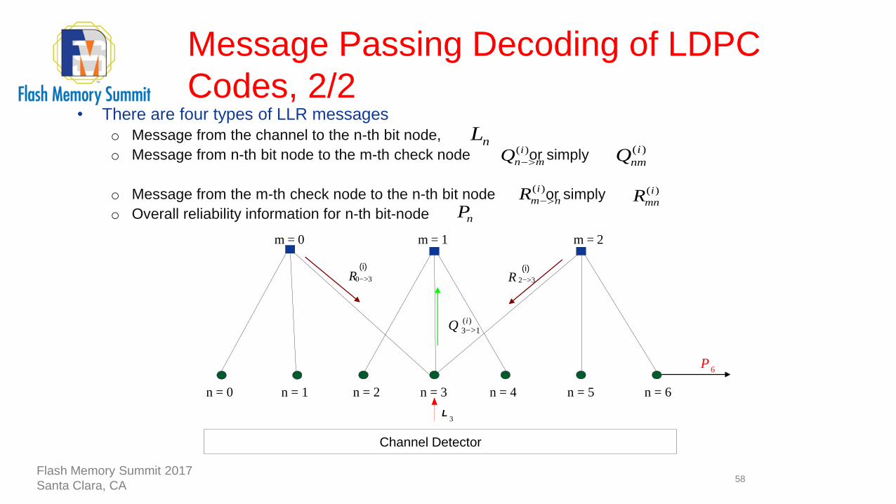
• There are four types of LLR messages
o Message from the channel to the n-th bit node,
o Message from n-th bit node to the m-th check node or simply
o Message from the m-th check node to the n-th bit node or simply
o Overall reliability information for n-th bit-node
Message Passing Decoding of LDPC
Codes, 2/2
58
( )i
n mQ >
( )i
m nR >
nL
nP
( )i
nmQ
( )i
mnR
33>
(i)
0R(i)
Channel Detector
)(
13
iQ >
R
n = 1
>
m = 2m = 1m = 0
L3
2
6P
n = 0 n = 2 n = 3 n = 4 n = 5 n = 6
Flash Memory Summit 2017
Santa Clara, CA

The Min-Sum Algorithm, 1/3
5959
Notation used in the equations
nx is the transmitted bit n ,
nL is the initial LLR message for a bit node (also called as variable node) n ,
received from channel/detector
nP is the overall LLR message for a bit node n ,
nx is the decoded bit n (hard decision based on nP ) ,
[Frequency of P and hard decision update depends on decoding schedule]
)(n is the set of the neighboring check nodes for variable node n ,
)(m is the set of the neighboring bit nodes for check node m .
For the ith
iteration, inmQ is the LLR message from bit node n to check node m ,
imnR is the LLR message from check node m to bit node n .
Flash Memory Summit 2017
Santa Clara, CA
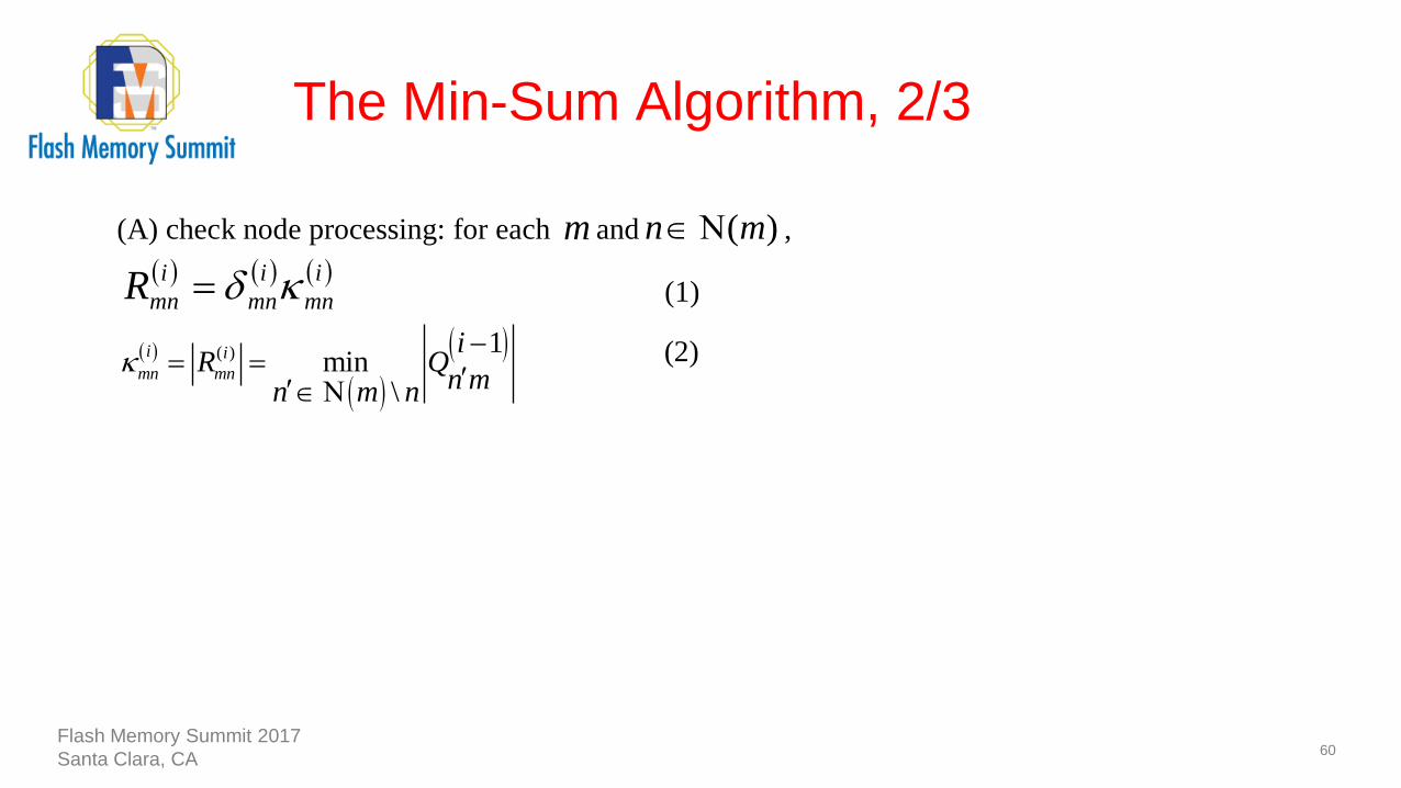
The Min-Sum Algorithm, 2/3
60
(A) check node processing: for each m and )(mn ,
imn
i
mn
i
mnR (1)
( ) 1min
\
i i
mn mn
iR Q
n mn m n
(2)
Flash Memory Summit 2017
Santa Clara, CA

The Min-Sum Algorithm, 2/3
61
(A) check node processing: for each m and )(mn ,
imn
i
mn
i
mnR (1)
( ) 1min
\
i i
mn mn
iR Q
n mn m n
(2)
The sign of check node message imnR is defined as
1
\
sgni i
mn n m
n m n
Q
(3)
where imn takes value of 1 or 1
Flash Memory Summit 2017
Santa Clara, CA
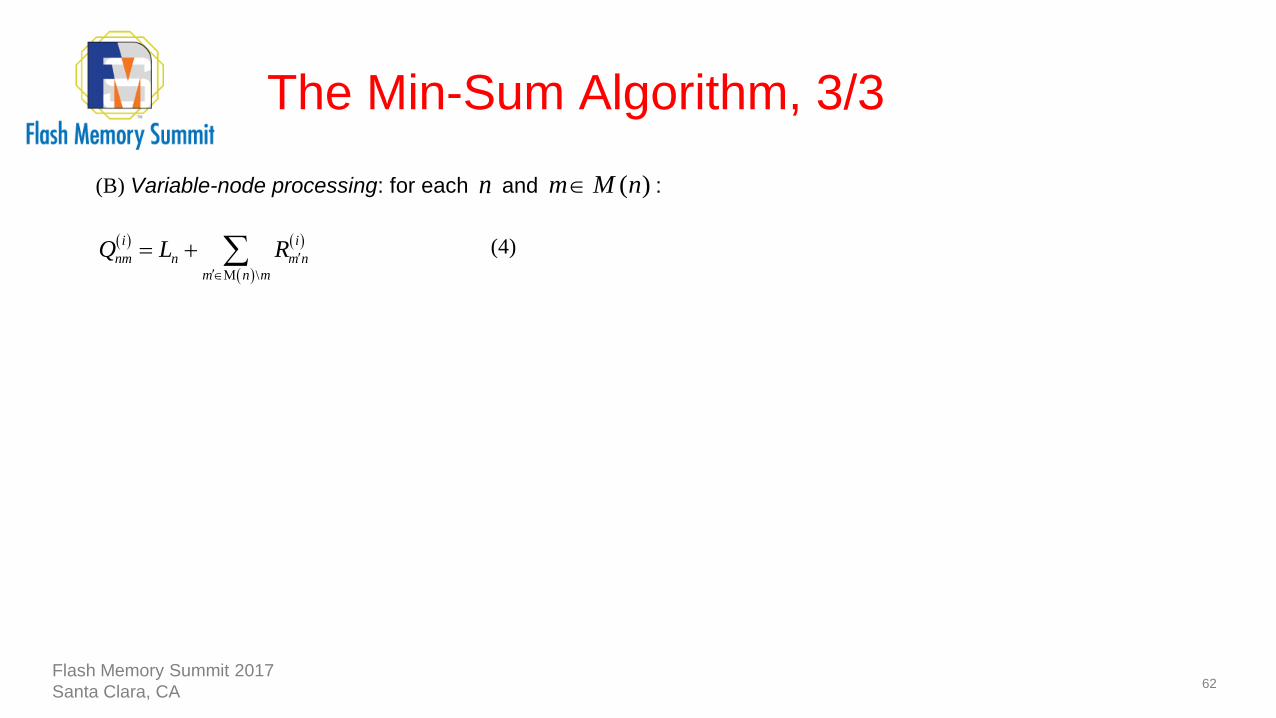
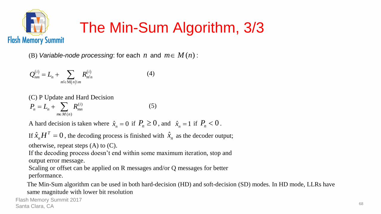
The Min-Sum Algorithm, 3/3
62
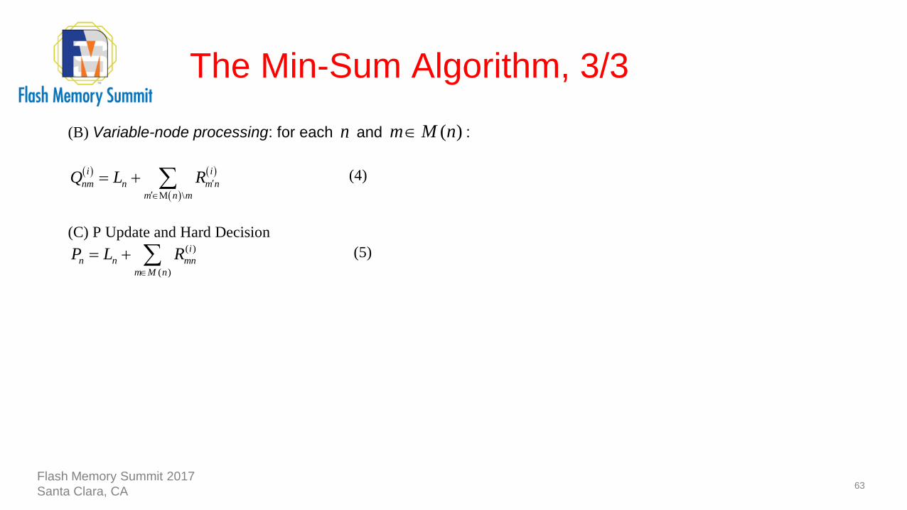
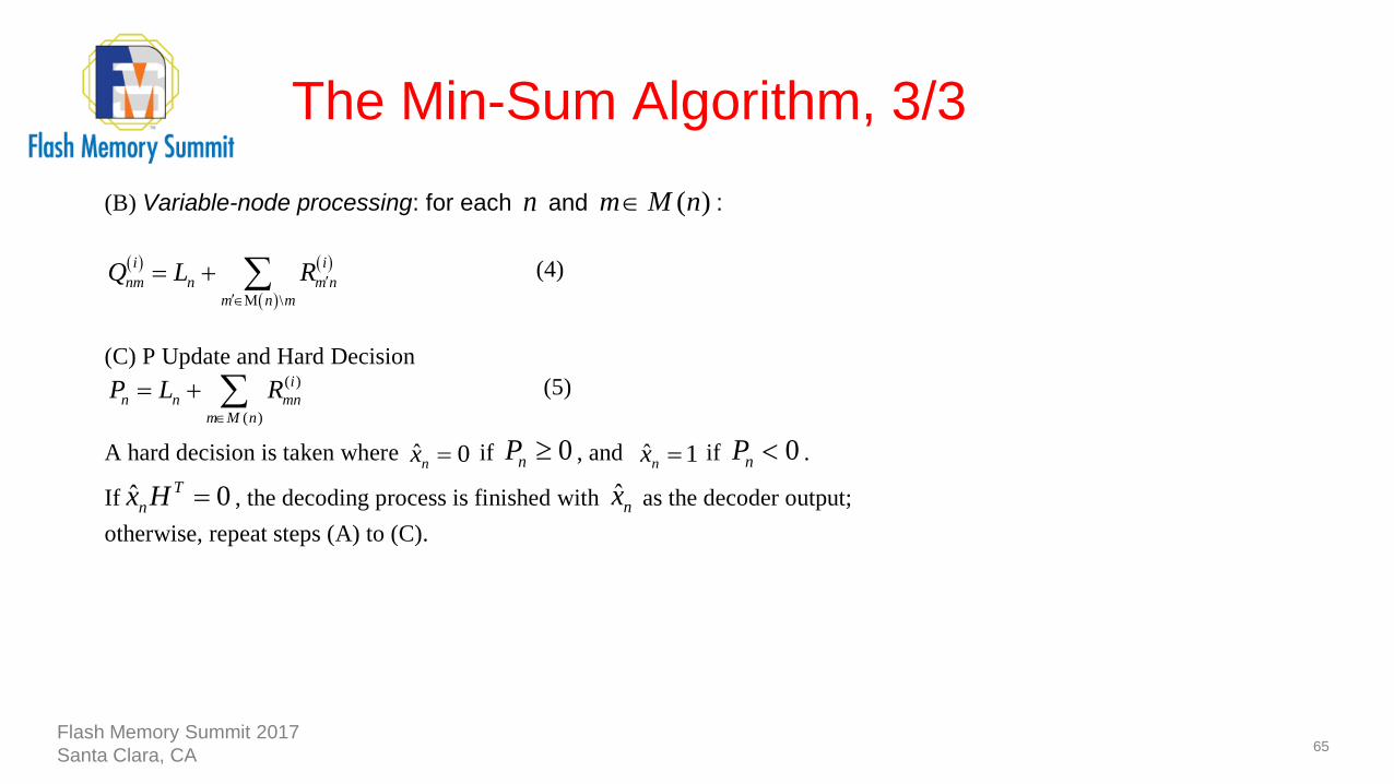
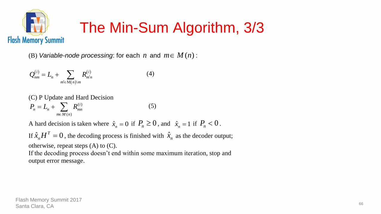
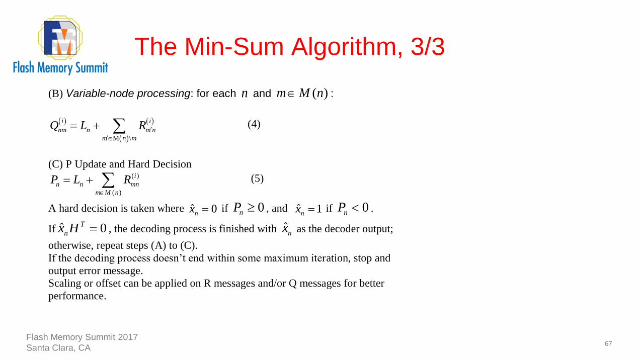
(B) Variable-node processing: for each n and ( )m M n :
\
i i
nm n m n
m n m
Q L R
(4)
Flash Memory Summit 2017
Santa Clara, CA
The Min-Sum Algorithm, 3/3
63
(B) Variable-node processing: for each n and ( )m M n :
\
i i
nm n m n
m n m
Q L R
(4)
(C) P Update and Hard Decision ( )
( )
i
n n mn
m M n
P L R
(5)
Flash Memory Summit 2017
Santa Clara, CA

The Min-Sum Algorithm, 3/3
64
(B) Variable-node processing: for each n and ( )m M n :
\
i i
nm n m n
m n m
Q L R
(4)
(C) P Update and Hard Decision ( )
( )
i
n n mn
m M n
P L R
(5)
A hard decision is taken where ˆ 0nx if 0nP , and ˆ 1nx if 0nP .
Flash Memory Summit 2017
Santa Clara, CA
The Min-Sum Algorithm, 3/3
65
(B) Variable-node processing: for each n and ( )m M n :
\
i i
nm n m n
m n m
Q L R
(4)
(C) P Update and Hard Decision ( )
( )
i
n n mn
m M n
P L R
(5)
A hard decision is taken where ˆ 0nx if 0nP , and ˆ 1nx if 0nP .
If ˆ 0T
nx H , the decoding process is finished with ˆnx as the decoder output;
otherwise, repeat steps (A) to (C).
Flash Memory Summit 2017
Santa Clara, CA
The Min-Sum Algorithm, 3/3
66
(B) Variable-node processing: for each n and ( )m M n :
\
i i
nm n m n
m n m
Q L R
(4)
(C) P Update and Hard Decision ( )
( )
i
n n mn
m M n
P L R
(5)
A hard decision is taken where ˆ 0nx if 0nP , and ˆ 1nx if 0nP .
If ˆ 0T
nx H , the decoding process is finished with ˆnx as the decoder output;
otherwise, repeat steps (A) to (C).
If the decoding process doesn’t end within some maximum iteration, stop and
output error message.
Flash Memory Summit 2017
Santa Clara, CA
The Min-Sum Algorithm, 3/3
67
(B) Variable-node processing: for each n and ( )m M n :
\
i i
nm n m n
m n m
Q L R
(4)
(C) P Update and Hard Decision ( )
( )
i
n n mn
m M n
P L R
(5)
A hard decision is taken where ˆ 0nx if 0nP , and ˆ 1nx if 0nP .
If ˆ 0T
nx H , the decoding process is finished with ˆnx as the decoder output;
otherwise, repeat steps (A) to (C).
If the decoding process doesn’t end within some maximum iteration, stop and
output error message.
Scaling or offset can be applied on R messages and/or Q messages for better
performance.
Flash Memory Summit 2017
Santa Clara, CA
The Min-Sum Algorithm, 3/3
68
(B) Variable-node processing: for each n and ( )m M n :
\
i i
nm n m n
m n m
Q L R
(4)
(C) P Update and Hard Decision ( )
( )
i
n n mn
m M n
P L R
(5)
A hard decision is taken where ˆ 0nx if 0nP , and ˆ 1nx if 0nP .
If ˆ 0T
nx H , the decoding process is finished with ˆnx as the decoder output;
otherwise, repeat steps (A) to (C).
If the decoding process doesn’t end within some maximum iteration, stop and
output error message.
Scaling or offset can be applied on R messages and/or Q messages for better
performance. The Min-Sum algorithm can be used in both hard-decision (HD) and soft-decision (SD) modes. In HD mode, LLRs have
same magnitude with lower bit resolution
Flash Memory Summit 2017
Santa Clara, CA
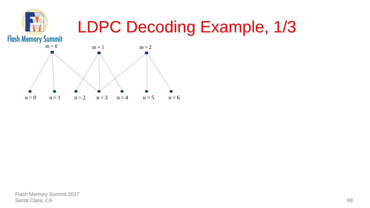
LDPC Decoding Example, 1/3
69
n = 1n = 0 n = 2 n = 3 n = 4 n = 5 n = 6
m = 0 m = 1 m = 2
Flash Memory Summit 2017
Santa Clara, CA
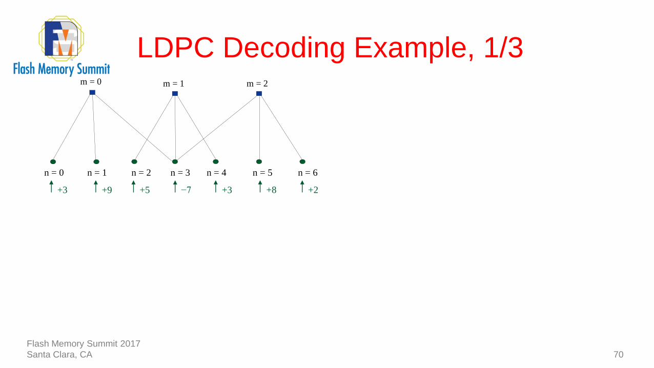
LDPC Decoding Example, 1/3
70
−7
n = 1n = 0 n = 2 n = 3 n = 4 n = 5 n = 6
+3 +8 +2+5+9+3
m = 0 m = 1 m = 2
Flash Memory Summit 2017
Santa Clara, CA

LDPC Decoding Example, 1/3
71
−7
n = 1n = 0 n = 2 n = 3 n = 4 n = 5 n = 6
+3 +8 +2+5+9+3
m = 0 m = 1 m = 2
Flash Memory Summit 2017
Santa Clara, CA

LDPC Decoding Example, 1/3
72
−7
n = 1n = 0 n = 2 n = 3 n = 4 n = 5 n = 6
+3 +8 +2+5+9+3
−7
+3−7
+2
−7
+9+3
+5
+8
m = 0 m = 1 m = 2Variable node
processing:
Flash Memory Summit 2017
Santa Clara, CA
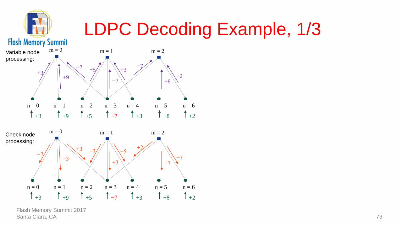
LDPC Decoding Example, 1/3
73
−7
n = 1n = 0 n = 2 n = 3 n = 4 n = 5 n = 6
+3 +8 +2+5+9+3
−7
+3−7
+2
−7
+9+3
+5
+8
m = 0 m = 1 m = 2Variable node
processing:
−7
n = 1n = 0 n = 2 n = 3 n = 4 n = 5 n = 6
+3 +8 +2+5+9+3
+3
−5+2
−7
+3
−3−7
−3
−7
m = 0 m = 1 m = 2Check node
processing:
Flash Memory Summit 2017
Santa Clara, CA

LDPC Decoding Example, 1/3
74
−7
n = 1n = 0 n = 2 n = 3 n = 4 n = 5 n = 6
+3 +8 +2+5+9+3
−7
+3−7
+2
−7
+9+3
+5
+8
m = 0 m = 1 m = 2Variable node
processing:
−7
n = 1n = 0 n = 2 n = 3 n = 4 n = 5 n = 6
+3 +8 +2+5+9+3
+3
−5+2
−7
+3
−3−7
−3
−7
m = 0 m = 1 m = 2Check node
processing:
−7
n = 1n = 0 n = 2 n = 3 n = 4 n = 5 n = 6
+3 +8 +2+5+9+3
+3
−5+2
−7
+3
−3−7
−3
−7
m = 0 m = 1 m = 2
+1 −3 +1 −5+2+6−4
P and HD
update:
P
Flash Memory Summit 2017
Santa Clara, CA
LDPC Decoding Example, 1/3
75
−7
n = 1n = 0 n = 2 n = 3 n = 4 n = 5 n = 6
+3 +8 +2+5+9+3
−7
+3−7
+2
−7
+9+3
+5
+8
m = 0 m = 1 m = 2Variable node
processing:
−7
n = 1n = 0 n = 2 n = 3 n = 4 n = 5 n = 6
+3 +8 +2+5+9+3
+3
−5+2
−7
+3
−3−7
−3
−7
m = 0 m = 1 m = 2Check node
processing:
−7
n = 1n = 0 n = 2 n = 3 n = 4 n = 5 n = 6
+3 +8 +2+5+9+3
+3
−5+2
−7
+3
−3−7
−3
−7
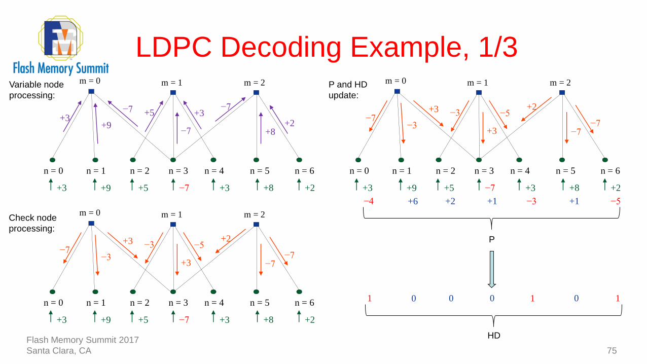
m = 0 m = 1 m = 2
+1 −3 +1 −5+2+6−4
P and HD
update:
P
0 1 0 1001
HDFlash Memory Summit 2017
Santa Clara, CA
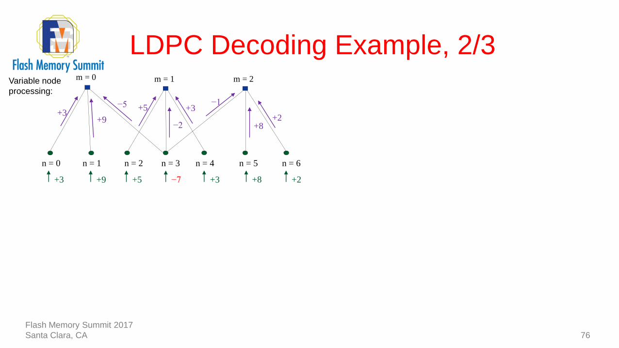
LDPC Decoding Example, 2/3
76
−7
n = 1n = 0 n = 2 n = 3 n = 4 n = 5 n = 6
+3 +8 +2+5+9+3
−2
+3−1
+2
−5
+9+3
+5
+8
m = 0 m = 1 m = 2Variable node
processing:
Flash Memory Summit 2017
Santa Clara, CA
LDPC Decoding Example, 2/3
77
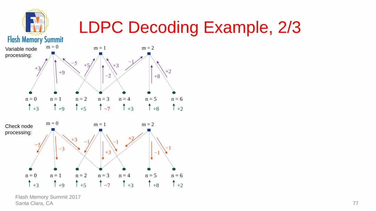
−7
n = 1n = 0 n = 2 n = 3 n = 4 n = 5 n = 6
+3 +8 +2+5+9+3
−2
+3−1
+2
−5
+9+3
+5
+8
m = 0 m = 1 m = 2Variable node
processing:
−7
n = 1n = 0 n = 2 n = 3 n = 4 n = 5 n = 6
+3 +8 +2+5+9+3
+3
−1+2
−1
+3
−3−5
−1
−1
m = 0 m = 1 m = 2Check node
processing:
Flash Memory Summit 2017
Santa Clara, CA
LDPC Decoding Example, 2/3
78
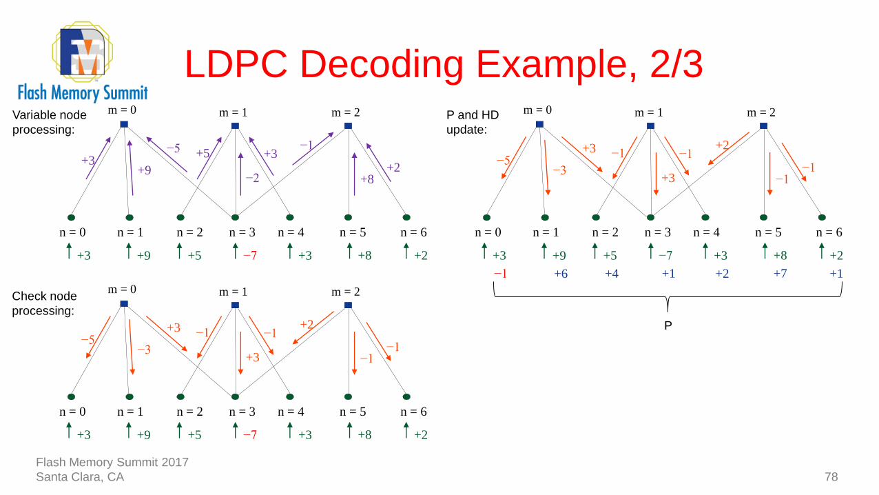
−7
n = 1n = 0 n = 2 n = 3 n = 4 n = 5 n = 6
+3 +8 +2+5+9+3
−2
+3−1
+2
−5
+9+3
+5
+8
m = 0 m = 1 m = 2Variable node
processing:
−7
n = 1n = 0 n = 2 n = 3 n = 4 n = 5 n = 6
+3 +8 +2+5+9+3
+3
−1+2
−1
+3
−3−5
−1
−1
m = 0 m = 1 m = 2Check node
processing:
−7
n = 1n = 0 n = 2 n = 3 n = 4 n = 5 n = 6
+3 +8 +2+5+9+3
+3
−1+2
−1
+3
−3−5
−1
−1
m = 0 m = 1 m = 2
+1 +2 +7 +1+4+6−1
P and HD
update:
P
Flash Memory Summit 2017
Santa Clara, CA

LDPC Decoding Example, 2/3
79
−7
n = 1n = 0 n = 2 n = 3 n = 4 n = 5 n = 6
+3 +8 +2+5+9+3
−2
+3−1
+2
−5
+9+3
+5
+8
m = 0 m = 1 m = 2Variable node
processing:
−7
n = 1n = 0 n = 2 n = 3 n = 4 n = 5 n = 6
+3 +8 +2+5+9+3
+3
−1+2
−1
+3
−3−5
−1
−1
m = 0 m = 1 m = 2Check node
processing:
−7
n = 1n = 0 n = 2 n = 3 n = 4 n = 5 n = 6
+3 +8 +2+5+9+3
+3
−1+2
−1
+3
−3−5
−1
−1
m = 0 m = 1 m = 2
+1 +2 +7 +1+4+6−1
P and HD
update:
P
0 0 0 0001
HDFlash Memory Summit 2017
Santa Clara, CA

LDPC Decoding Example, 3/3
80
−7
n = 1n = 0 n = 2 n = 3 n = 4 n = 5 n = 6
+3 +8 +2+5+9+3
−2
+3−1
+2
−2
+9+3
+5
+8
m = 0 m = 1 m = 2Variable node
processing:
Flash Memory Summit 2017
Santa Clara, CA

LDPC Decoding Example, 3/3
81
−7
n = 1n = 0 n = 2 n = 3 n = 4 n = 5 n = 6
+3 +8 +2+5+9+3
−2
+3−1
+2
−2
+9+3
+5
+8
m = 0 m = 1 m = 2Variable node
processing:
−7
n = 1n = 0 n = 2 n = 3 n = 4 n = 5 n = 6
+3 +8 +2+5+9+3
+3
−2+2
−1
+3
−2−2
−2
−1
m = 0 m = 1 m = 2Check node
processing:
Flash Memory Summit 2017
Santa Clara, CA

LDPC Decoding Example, 3/3
82
−7
n = 1n = 0 n = 2 n = 3 n = 4 n = 5 n = 6
+3 +8 +2+5+9+3
−2
+3−1
+2
−2
+9+3
+5
+8
m = 0 m = 1 m = 2Variable node
processing:
−7
n = 1n = 0 n = 2 n = 3 n = 4 n = 5 n = 6
+3 +8 +2+5+9+3
+3
−2+2
−1
+3
−2−2
−2
−1
m = 0 m = 1 m = 2Check node
processing:
−7
n = 1n = 0 n = 2 n = 3 n = 4 n = 5 n = 6
+3 +8 +2+5+9+3
+3
−2+2
−1
+3
−2−2
−2
−1
m = 0 m = 1 m = 2
+1 +1 +7 +1+3+7+1
P and HD
update:
P
Flash Memory Summit 2017
Santa Clara, CA
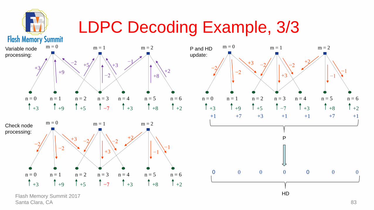
LDPC Decoding Example, 3/3
83
−7
n = 1n = 0 n = 2 n = 3 n = 4 n = 5 n = 6
+3 +8 +2+5+9+3
−2
+3−1
+2
−2
+9+3
+5
+8
m = 0 m = 1 m = 2Variable node
processing:
−7
n = 1n = 0 n = 2 n = 3 n = 4 n = 5 n = 6
+3 +8 +2+5+9+3
+3
−2+2
−1
+3
−2−2
−2
−1
m = 0 m = 1 m = 2Check node
processing:
−7
n = 1n = 0 n = 2 n = 3 n = 4 n = 5 n = 6
+3 +8 +2+5+9+3
+3
−2+2
−1
+3
−2−2
−2
−1
m = 0 m = 1 m = 2
+1 +1 +7 +1+3+7+1
P and HD
update:
P
0 0 0 0000
HDFlash Memory Summit 2017
Santa Clara, CA
Overview
84
• Why Is Error Correction Needed in Flash Memories?
• Error Correction Codes Fundamentals
• Low-Density Parity-Check (LDPC) Codes
• LDPC Encoding and Decoding Methods
• Decoder Architectures for LDPC Codes
Flash Memory Summit 2017
Santa Clara, CA
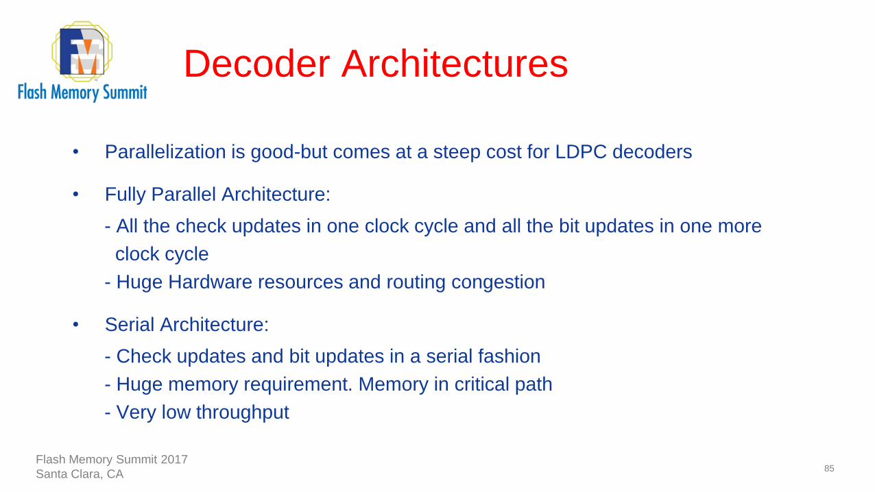
Decoder Architectures
• Parallelization is good-but comes at a steep cost for LDPC decoders
• Fully Parallel Architecture:
- All the check updates in one clock cycle and all the bit updates in one more
clock cycle
- Huge Hardware resources and routing congestion
• Serial Architecture:
- Check updates and bit updates in a serial fashion
- Huge memory requirement. Memory in critical path
- Very low throughput
85Flash Memory Summit 2017
Santa Clara, CA

Semi-parallel Architectures
• Check updates and bit updates using several units.
• Partitioned memory by imposing structure on H matrix.
• Practical solution for most of the applications.
• There are several semi-parallel architectures proposed.
• Complexity differs based on architecture and scheduling.
86Flash Memory Summit 2017
Santa Clara, CA
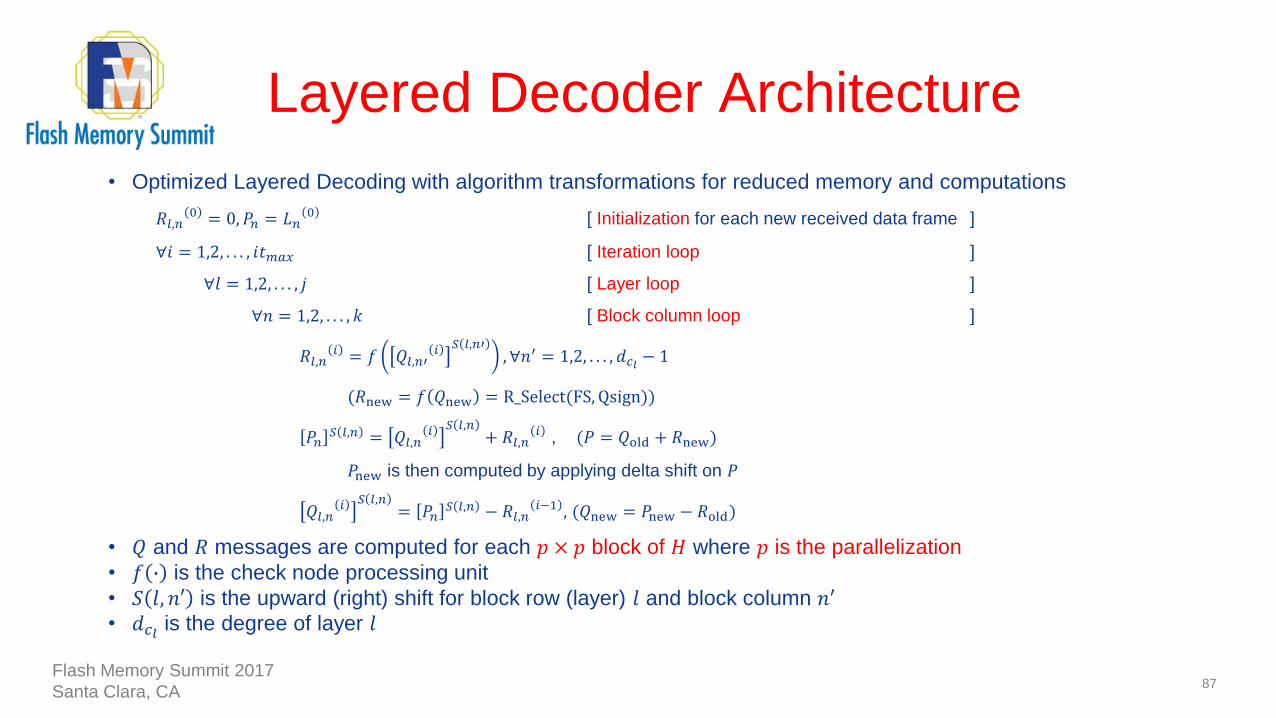
Layered Decoder Architecture
87
• Optimized Layered Decoding with algorithm transformations for reduced memory and computations
𝑅𝑙,𝑛0 = 0, 𝑃𝑛 = 𝐿𝑛
0 [ Initialization for each new received data frame ]
∀𝑖 = 1,2, . . . , 𝑖𝑡𝑚𝑎𝑥 [ Iteration loop ]
∀𝑙 = 1,2, . . . , 𝑗 [ Layer loop ]
∀𝑛 = 1,2, . . . , 𝑘 [ Block column loop ]
𝑅𝑙,𝑛𝑖 = 𝑓 𝑄𝑙,𝑛′
𝑖 𝑆 𝑙,𝑛′, ∀𝑛′ = 1,2, . . . , 𝑑𝑐𝑙 − 1
(𝑅new = 𝑓 𝑄new = R_Select(FS, Qsign))
𝑃𝑛𝑆 𝑙,𝑛 = 𝑄𝑙,𝑛
𝑖 𝑆 𝑙,𝑛+ 𝑅𝑙,𝑛
𝑖 , (𝑃 = 𝑄old + 𝑅new)
𝑃new is then computed by applying delta shift on 𝑃
𝑄𝑙,𝑛𝑖 𝑆 𝑙,𝑛
= 𝑃𝑛𝑆 𝑙,𝑛 − 𝑅𝑙,𝑛
𝑖−1 , (𝑄new = 𝑃new − 𝑅old)
• 𝑄 and 𝑅 messages are computed for each 𝑝 × 𝑝 block of 𝐻 where 𝑝 is the parallelization
• 𝑓 ∙ is the check node processing unit
• 𝑆 𝑙, 𝑛′ is the upward (right) shift for block row (layer) 𝑙 and block column 𝑛′
• 𝑑𝑐𝑙 is the degree of layer 𝑙
Flash Memory Summit 2017
Santa Clara, CA

Block Serial Layered Decoder Architecture
with On-the-Fly Computation
88
See [8, P1-P6] and references therein for more
details on features and implementation.
• Proposed for irregular H matrices
• Goal: minimize memory and re-computations by employing
just in-time scheduling
• Advantages compared to other architectures:
1) Q memory (or L/P/Q memory) can be used to store
L/Q/P instead of 3 separate memories- memory is
managed at circulant level as at any time for a given
circulant we need only L or Q or P.
2) Only one shifter.
3) Value-reuse is effectively used for both Rnew and Rold
4) Low complexity data path design-with no redundant
data path operations.
5) Low complexity CNU design.
6) Out-of-order processing at both layer and circulant level
for all the processing steps such as Rnew and PS
processing to eliminate the pipeline and memory
access stall cycles.Flash Memory Summit 2017
Santa Clara, CA
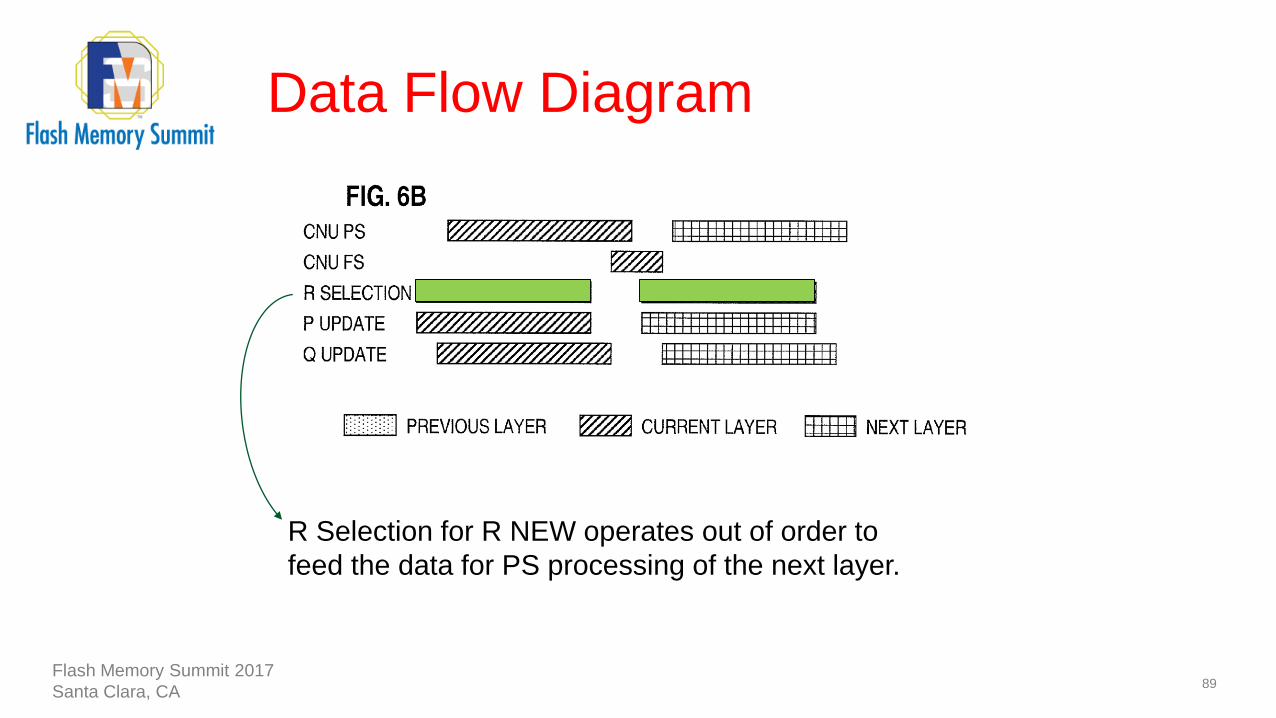
Data Flow Diagram
89
R Selection for R NEW operates out of order to
feed the data for PS processing of the next layer.
Flash Memory Summit 2017
Santa Clara, CA

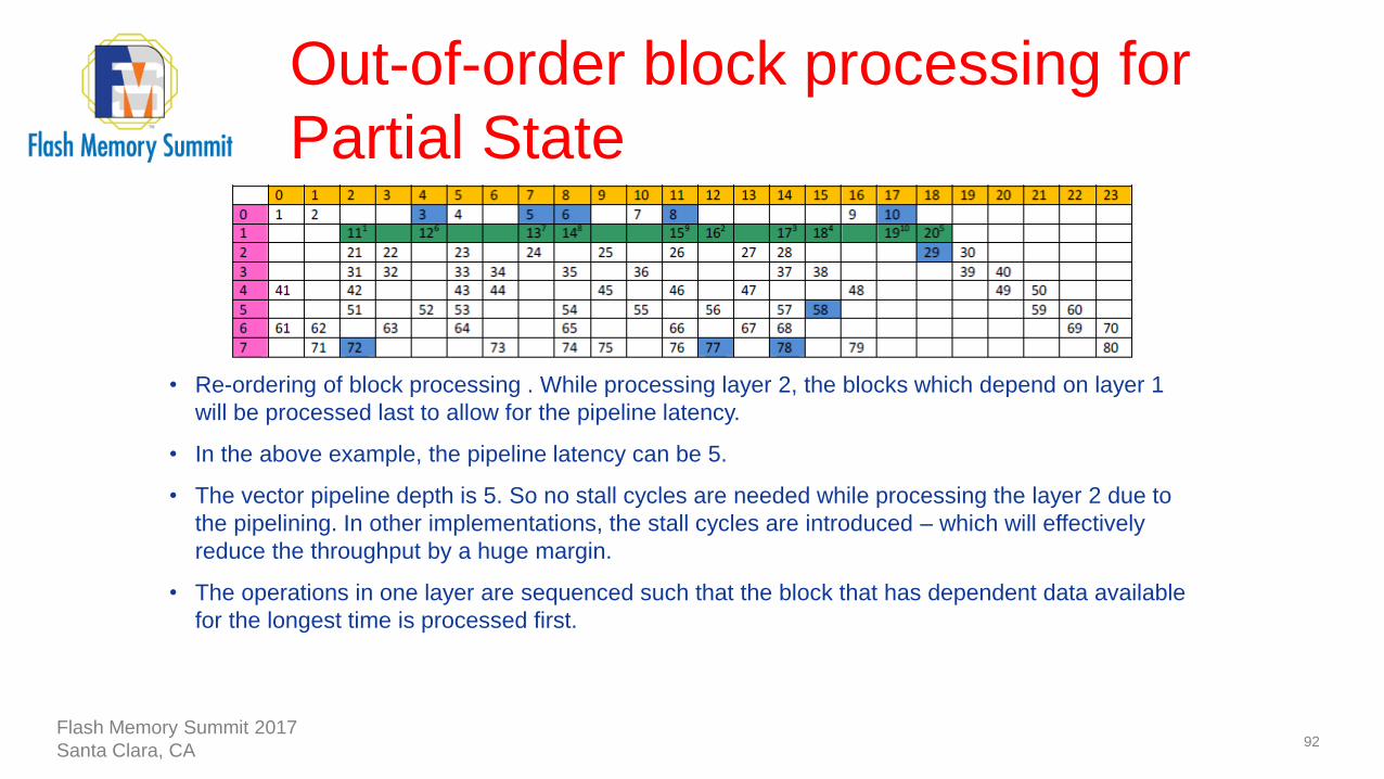
Illustration for out-of-order
processing
90
• Rate 2/3 code. 8 Layers, 24 block columns. dv, column weight varies from 2 to 6. dc, row weight is 10 for all
the layers.
• Non-zero circulants are numbered from 1 to 80. No layer re-ordering in processing. Out-of-order processing
for Rnew. Out-of-order processing for Partial state processing.
• Illustration for 2nd iteration with focus on PS processing of 2nd layer.
• Rold processing is based on the circulant order 11 16 17 18 20 12 13 14 15 19 and is
indicated in green.
• Rnew is based on the circulant order 72 77 78 58 29 3 5 6 8 10 and is indicated in blue.
• Q memory, HD memory access addresses are based on the block column index to which the green
circulants are connected to.
• Q sign memory access address is based on green circulant number.
• Superscript indicates the clock cycle number counted from 1 at the beginning of layer 2 processing.
Flash Memory Summit 2017
Santa Clara, CA
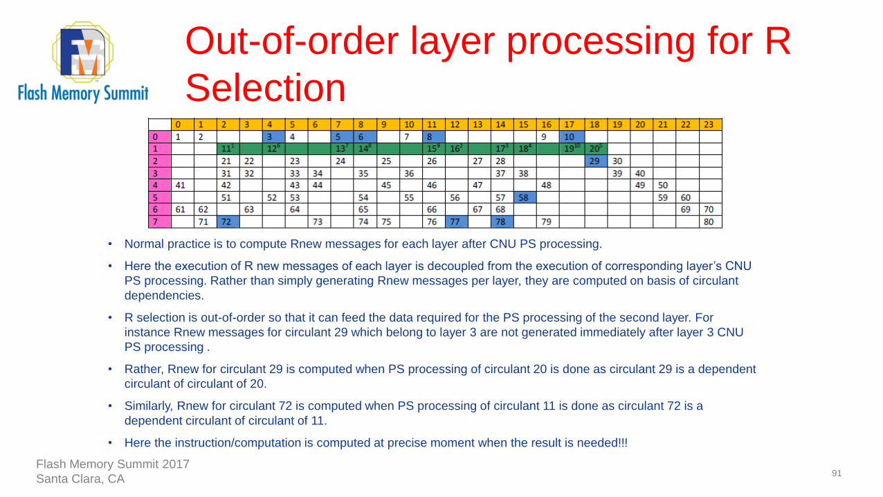
Out-of-order layer processing for R
Selection
91
• Normal practice is to compute Rnew messages for each layer after CNU PS processing.
• Here the execution of R new messages of each layer is decoupled from the execution of corresponding layer’s CNU
PS processing. Rather than simply generating Rnew messages per layer, they are computed on basis of circulant
dependencies.
• R selection is out-of-order so that it can feed the data required for the PS processing of the second layer. For
instance Rnew messages for circulant 29 which belong to layer 3 are not generated immediately after layer 3 CNU
PS processing .
• Rather, Rnew for circulant 29 is computed when PS processing of circulant 20 is done as circulant 29 is a dependent
circulant of circulant of 20.
• Similarly, Rnew for circulant 72 is computed when PS processing of circulant 11 is done as circulant 72 is a
dependent circulant of circulant of 11.
• Here the instruction/computation is computed at precise moment when the result is needed!!!
Flash Memory Summit 2017
Santa Clara, CA
Out-of-order block processing for
Partial State
92
• Re-ordering of block processing . While processing layer 2, the blocks which depend on layer 1
will be processed last to allow for the pipeline latency.
• In the above example, the pipeline latency can be 5.
• The vector pipeline depth is 5. So no stall cycles are needed while processing the layer 2 due to
the pipelining. In other implementations, the stall cycles are introduced – which will effectively
reduce the throughput by a huge margin.
• The operations in one layer are sequenced such that the block that has dependent data available
for the longest time is processed first.
Flash Memory Summit 2017
Santa Clara, CA
Memory organization
• Q memory width is equal to circulant size * 8 bits and depth is number of block columns.
• HD memory width is equal to circulant size * 1 bits and depth is number of block columns.
• Qsign memory width is equal to circulant size * 1 bits and depth is number of non-zero
circulants in H-matrix.
• FS memory width is equal to circulant size * (15 bits (= 4 bits for Min1 + 4 bits for Min2 index
+ 1 bit + 6 bits for Min1 index).
• FS memory access is expensive and number of accesses can be reduced with scheduling.
• For the case of decoder for regular mother matrices (no 0 blocks and no OOP): FS access is
needed one time for Rold for each layer; is needed one time for R new for each layer.
• For the case of decoder for irregular mother matrices: FS access is needed one time for
Rold for each layer; is needed one time for R new for each non-zero circulant in each layer.
93Flash Memory Summit 2017
Santa Clara, CA
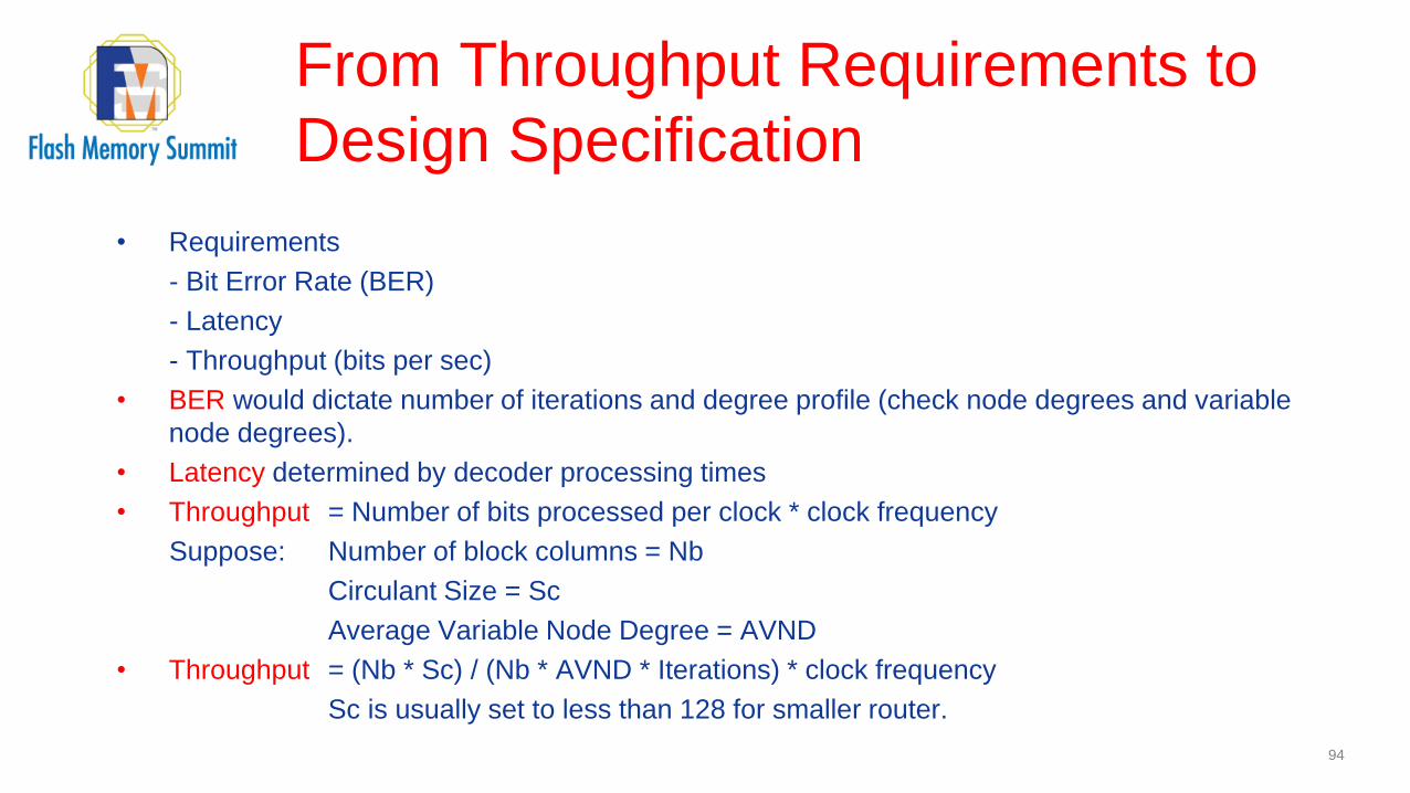
From Throughput Requirements to
Design Specification
• Requirements
- Bit Error Rate (BER)
- Latency
- Throughput (bits per sec)
• BER would dictate number of iterations and degree profile (check node degrees and variable
node degrees).
• Latency determined by decoder processing times
• Throughput = Number of bits processed per clock * clock frequency
Suppose: Number of block columns = Nb
Circulant Size = Sc
Average Variable Node Degree = AVND
• Throughput = (Nb * Sc) / (Nb * AVND * Iterations) * clock frequency
Sc is usually set to less than 128 for smaller router.
94
References1. Y. Cai, E. F. Haratsch, et al., “Threshold Voltage Distribution in MLC NAND Flash Memory:
Characterization, Analysis, and Modeling,” Proceedings of the Conference on Design, Automation and Testin Europe. EDA Consortium, 2013.
2. R. Tanner, “A recursive approach to low-complexity codes,” IEEE Trans. on info. Theory, 27.5, pp. 533-547, 1981.
3. R. G. Gallager, “Low density parity check codes,” IRE Trans. Info. Theory, IT-8:21-28, Jan 1962.
4. R. G. Gallager, Low-Density Parity-Check Codes. Cambridge, MA: MIT Press, 1963.
5. W. Ryan and S. Lin, Channel codes: classical and modern, Cambridge University Press, 2009.
6. Levine, et. al., “Implementation of near Shannon limit error-correcting codes using reconfigurable hardware,”IEEE Field-Programmable Custom Computing Machine, 2000.
7. E. Yeo, “VLSI architectures for iterative decoders in magnetic recording channels,” IEEE Trans. Magnetics,vol. 37, no.2, pp. 748-55, March 2001.
8. K. K. Gunnam, “LDPC Decoding: VLSI Architectures and Implementations,” Flash Memory Summit, 2013.
95
Some of these slides are used from other references with permission.
Flash Memory Summit 2017
Santa Clara, CA

References
Several features presented in this tutorial are covered by the following
patents by Texas A&M University System (TAMUS):
[P1] U.S. Patent 8359522, Low density parity check decoder for regular LDPC codes.
[P2] U.S. Patent 8418023, Low density parity check decoder for irregular LDPC codes.
[P3] U.S. Patent 8555140, Low density parity check decoder for irregular LDPC codes.
[P4] U.S. Patent 8656250,Low density parity check decoder for regular LDPC codes.
[P5] U.S. Patent 9112530, Low density parity check decoder.
[P6] U.S. Patent 20150311917, Low density parity check decoder.
96
Some of these slides are used from other references with permission.
Flash Memory Summit 2017
Santa Clara, CA