EC6404 LINEAR INTEGRATED CIRCUITS L T P C 3 0 0 3 ...Closed loop analysis, Voltage controlled...
353
Syllabus EC6404 LINEAR INTEGRATED CIRCUITS L T P C 3 0 0 3 UNIT I BASICS OF OPERATIONAL AMPLIFIERS 9 Current mirror and current sources, Current sources as active loads, Voltage sources, Voltage References, BJT Differential amplifier with active loads, Basic information about op-amps – Ideal Operational Amplifier - General operational amplifier stages -and internal circuit diagrams of IC 741,DC and AC performance characteristics, slew rate, Open and closed loop configurations. UNIT II APPLICATIONS OF OPERATIONAL AMPLIFIERS 9 Sign Changer, Scale Changer, Phase Shift Circuits, Voltage Follower, V-to-I and I-to-V converters, adder, subtractor, Instrumentation amplifier, Integrator, Differentiator, Logarithmic amplifier,Antilogarithmic amplifier, Comparators, Schmitt trigger, Precision rectifier, peak detector, clipper and clamper, Low-pass, high-pass and band-pass Butterworth filters. UNIT III ANALOG MULTIPLIER AND PLL 9 Analog Multiplier using Emitter Coupled Transistor Pair - Gilbert Multiplier cell – Variable transconductance technique, analog multiplier ICs and their applications, Operation of the basic PLL,Closed loop analysis, Voltage controlled oscillator, Monolithic PLL IC 565, application of PLL for AM detection, FM detection, FSK modulation and demodulation and Frequency synthesizing. UNIT IV ANALOG TO DIGITAL AND DIGITAL TO ANALOG CONVERTERS 9 Analog and Digital Data Conversions, D/A converter – specifications - weighted resistor type, R-2R Ladder type, Voltage Mode and Current-Mode R 2R Ladder types - switches for D/A converters, high speed sample-and-hold circuits, A/D Converters – specifications - Flash type – Successive Approximation type - Single Slope type – Dual Slope type - A/D Converter using Voltage-to-Time Conversion - Over-sampling A/D Converters. UNIT V WAVEFORM GENERATORS AND SPECIAL FUNCTION ICS 9 Sine-wave generators, Multivibrators and Triangular wave generator, Saw-tooth wave generator, ICL8038 function generator, Timer IC 555, IC Voltage regulators – Three terminal fixed and adjustable voltage regulators - IC 723 general purpose regulator - Monolithic switching regulator, Switched capacitor filter IC MF10, Frequency to Voltage and Voltage to Frequency converters, Audio Power amplifier, Video Amplifier, Isolation Amplifier, Opto-couplers and fibre optic IC. TOTAL: 45 PERIODS . TEXT BOOKS: 1. D.Roy Choudhry, Shail Jain, “Linear Integrated Circuits”, New Age International Pvt. Ltd., 2000. 2. Sergio Franco, “Design with Operational Amplifiers and Analog Integrated Circuits”, 3rd Edition, Tata Mc Graw-Hill, 2007. REFERENCES: 1. Ramakant A. Gayakwad, “OP-AMP and Linear ICs”, 4th Edition, Prentice Hall / Pearson Education, 2001. 2. Robert F.Coughlin, Frederick F.Driscoll, “Operational Amplifiers and Linear Integrated Circuits”,Sixth Edition, PHI, 2001.
Transcript of EC6404 LINEAR INTEGRATED CIRCUITS L T P C 3 0 0 3 ...Closed loop analysis, Voltage controlled...

Syllabus
EC6404 LINEAR INTEGRATED CIRCUITS L T P C
3 0 0 3
UNIT I BASICS OF OPERATIONAL AMPLIFIERS 9
Current mirror and current sources, Current sources as active loads, Voltage sources, Voltage
References, BJT Differential amplifier with active loads, Basic information about op-amps – Ideal
Operational Amplifier - General operational amplifier stages -and internal circuit diagrams of IC
741,DC and AC performance characteristics, slew rate, Open and closed loop configurations.
UNIT II APPLICATIONS OF OPERATIONAL AMPLIFIERS 9
Sign Changer, Scale Changer, Phase Shift Circuits, Voltage Follower, V-to-I and I-to-V converters,
adder, subtractor, Instrumentation amplifier, Integrator, Differentiator, Logarithmic
amplifier,Antilogarithmic amplifier, Comparators, Schmitt trigger, Precision rectifier, peak detector,
clipper and clamper, Low-pass, high-pass and band-pass Butterworth filters.
UNIT III ANALOG MULTIPLIER AND PLL 9
Analog Multiplier using Emitter Coupled Transistor Pair - Gilbert Multiplier cell – Variable
transconductance technique, analog multiplier ICs and their applications, Operation of the basic
PLL,Closed loop analysis, Voltage controlled oscillator, Monolithic PLL IC 565, application of PLL
for AM detection, FM detection, FSK modulation and demodulation and Frequency synthesizing.
UNIT IV ANALOG TO DIGITAL AND DIGITAL TO ANALOG CONVERTERS 9
Analog and Digital Data Conversions, D/A converter – specifications - weighted resistor type, R-2R
Ladder type, Voltage Mode and Current-Mode R 2R Ladder types - switches for D/A converters,
high speed sample-and-hold circuits, A/D Converters – specifications - Flash type – Successive
Approximation type - Single Slope type – Dual Slope type - A/D Converter using Voltage-to-Time
Conversion - Over-sampling A/D Converters.
UNIT V WAVEFORM GENERATORS AND SPECIAL FUNCTION ICS 9
Sine-wave generators, Multivibrators and Triangular wave generator, Saw-tooth wave generator,
ICL8038 function generator, Timer IC 555, IC Voltage regulators – Three terminal fixed and
adjustable voltage regulators - IC 723 general purpose regulator - Monolithic switching regulator,
Switched capacitor filter IC MF10, Frequency to Voltage and Voltage to Frequency converters,
Audio Power amplifier, Video Amplifier, Isolation Amplifier, Opto-couplers and fibre optic IC.
TOTAL: 45 PERIODS
.
TEXT BOOKS:
1. D.Roy Choudhry, Shail Jain, “Linear Integrated Circuits”, New Age International Pvt. Ltd.,
2000.
2. Sergio Franco, “Design with Operational Amplifiers and Analog Integrated Circuits”, 3rd Edition,
Tata Mc Graw-Hill, 2007.
REFERENCES:
1. Ramakant A. Gayakwad, “OP-AMP and Linear ICs”, 4th Edition, Prentice Hall / Pearson
Education, 2001.
2. Robert F.Coughlin, Frederick F.Driscoll, “Operational Amplifiers and Linear Integrated
Circuits”,Sixth Edition, PHI, 2001.

Unit-1
CURRENT MIRROR AND CURRENT SOURCES:
Constant current source(Current Mirror): A constant current source makes use of the fact that for a transistor in the active mode of
operation, the collector current is relatively independent of the collector voltage. In the basic
circuit shown in fig 1
Transistors Q1&Q2 are matched as the circuit is fabricated using IC technology. Base and
emitter of Q1&Q2 are tied together and thus have the same VBE. .In addition, transistor Q1 is
connected as a diode by shorting it s collector to base. The input current Iref flows through the
diode connected transistor Q1 and thus establishes a voltage across Q1.
This voltage in turn appears between the base and emitter of Q2 .Since Q2 is identical to
Q1, the emitter current of Q2 will be equal to emitter current of Q1 which is approximately equal to
Iref
As long as Q2 is maintained in the active region ,its collector current IC2=Io will
be approximately equal to Iref .
Since the output current Io is a reflection or mirror of the reference current Iref, the circuit is
often referred to as a current mirror.
Analysis:
The collector current IC1 and IC2 for the transistor Q1 and Q2 can be approximately
expressed as
IC1 t
V
BfffEffff1fffff
V T
F ES
---------(1)
IC2 t V
BfffEffff2ffffff
V T ------------(2)
F ES
From equation (1)&(2)

V fBfEf2 f@
fV fBfEf1 f
IfCf2 f e V
T
IC1
-----------------(3)
Since VBE1=VBE2 we obtain
IC2=IC1=IC=IO
Also since both the transistors are identical , 1 2
KCL at the collector of Q1 gives
Iref= IC1+IB1+IB2
IC1
IfCff1f f IfCff2f f C
f g
1 2 f
1 2
solving Eq (4).
IC may be expressed as
----------(4)
f
IC 2 I ref ------------(5)
Where Iref from fig can be seen to be
I V V fBfE f
≈≈ 1
V fCfC f
R1
f
(as VBE=0.7V is small)
From Eq.5 for >>1, 2 is almost unity and the output current I0 is equal to the reference
current, Iref which for a given R1 is constant. Typically Io varies by about 3% for 50 ≤ ≤200.
It is possible to obtain current transfer ratio other than unity simple by controlling the area
of the emitter-base junction (EBJ) of the transistor Q2 . For example, if the area of EBJ of Q2 is
4 times that of Q1,then
IO=4 I ref
The output resistance of the current source is the output resistance,r0 of Q2,
R0=I02= V fAf f
IO
V ≈=
I fA f
ref
[VA is the Early voltage]

The circuit however operates as a constant current source as long as Q2 remains in the active
region.
Widlar current source:
Widlar current source which is particularly suitable for low value of currents. The circuit
differs from the basic current mirror only in the resistance RE that is included in the emitter lead of
Q2.
It can be seen that due to RE the base-emitter voltage VBE2 is les than VBE1 and
consequently current Io is smaller than IC1
The ratio of collector currents IC1&IC2 using
If f f V fBfEf2 f
@
C 2 e V
T
IC1
fV fBfEf1 f
------------(1)
Taking natural logarithm of both sides, we get
VBE1-VBE2=VT lnj
IfCff1f IC2
-------(2)
Writing KVL for the emitter base loop
VBE1=VBE2+(IB2+IC2)RE ----------------(3)
or VBE1-VBE2=(1/ +1)IC2RE -----------(4)
From eqn (2)&(4) we obtain
f g 1f
1 I c2 RE
IfCff1ff V T ln
I --------------(5)
Or
fV fT
C2
f IfCff1ff
RE
d e
1 1f
IC2
ln IC2
--------------(6)
A relation between IC1 and the reference current Iref is obtained by writing KCL at the
collector point of Q1
Iref= IC1+IB1+IB2

f
= IC1 1 1
g I C2f
----------------(7)
(Assuming 2 1 for identical transistors)
In the Widlar current source IC2<<IC1,therefore the term
g
IfCff2ff
may be neglected in (7)
f 1 f
Thus I ref t I
C1 1
fI
IC1= 1
Where I ref
ref
V fcfc f@f fV
R1
fBffEf f
For >>1 IC1 t I ref
Wilson current source:
The Wilson current source shown in fig
It provides an output current Io, which is very nearly equal to V ref and also exhibits a very
high output resistance.
Current sources as Active loads:
The current source can be used as an active load in both analog and digital IC’s. The active
load realized using current source in place of the passive load (i.e. a resistor) in the collector arm
of differential amplifier makes it possible to achieve high voltage gain without requiring large
power supply voltage. The active load so achieved is basically r0 of a PNP transistor.

Voltage Sources:
A voltage source is a circuit that produces an output voltage V0 , which is independent of
the load driven by the voltage source, or the output current supplied to the load. The voltage source
is the circuit dual of the constant current source.
A number of IC applications require a voltage reference point with very low ac impedance
and a stable dc voltage that is not affected by power supply and temperature variations. There are
two methods which can be used to produce a voltage source, namely,
1. using the impedance transforming properties of the transistor, which in turn determines the
current gain of the transistor and
2. using an amplifier with negative feedback.
Voltage source circuit using Impedance transformation:
The voltage source circuit using the impedance transforming property of the transistor is
shown in figure. The source voltage Vs drives the base of the transistor through a series resistance
RS and the output is taken across the emitter. From the circuit, the output ac resistance looking into
emitter is given by
dfV f0 f
0
fRfS f eb
dI 0 1
with values as high as 100 for , RS is transformed to a value of
fRfS fA
1
It is to be noted that, eqn is applicable only for small changes in the output current. The
load regulation parameter indicates the changes in V0 resulting from large changes in output
current I0 , Reduction in V0 occurs as I0 goes from no-load current to full-load current and this
factor determines the output impedance of the voltage sources.

Emitter – follower or Common Collector Type Voltage source:
The figure shows an emitter follower or common collector type voltage source. This voltage
source is suitable for the differential gain stage used in op-amps. This circuit has the advantages of
1. Producing low ac impedance and
2. resulting in effective decoupling of adjacent gain stages.
The low output impedance of the common-collector stage simulates a low impedance voltage
source with an output voltage level of V0 represented by
V 0 V c j
fRf2
R1
R2
The diode D1 is used for offsetting the effect of dc value VBE , across the E-B junction of the
transistor, and for compensating the temperature dependence of VBE drop of Q1. The load ZL shown
in dotted line represents the circuit biased by the current through Q1.
The impedance R0 looking into the emitter of Q1 derived from the hybrid π model is given by
R V fT f
0 1
fRf1 fRf2 f
b c
R1 R2
Voltage Source suing Temperature compensated Avalanche Diode:
The voltage source using common collector stage has the limitations of its vulnerability for
changes in bias voltage VN and the output voltage V0 with respect to changes in supply voltage
Vcc. This is overcome in the voltage source circuit using the breakdown voltage of the base-
emitter junction shown below.

The emitter – follower stage of common – collector is eliminated in this circuit, since the
impedance seen looking into the bias terminal N is very low. The current source I1 is normally
simulated by a resistor connected between Vcc and node n. Then, the output voltage level V0 at
node N is given by
V0 = VB +VBE
Where VB is the breakdown voltage of diode DB and VBE is the diode drop across D1.
The breakdown diode DB is normally realized using the base-emitter junction of the transistor.
The diode D1 provides partial compensation for the positive temperature coefficient effect of VB.
In a monolithic IC structure, DB and D1 can be conveniently realized as a single transistor with
two individual emitters as shown in figure.
Temperature Compensated avalanche diode Voltage source using
breakdown voltage of the
base- emitter junction
The structure consists of composite connection of two transistors which are diode-
connected back-to back. Since the transistors have their base to collector terminals common, they
can be designed as a single transistor with two emitters.
The output resistance R0 looking into the output terminal in figure is given by

R0 RB
V fT f
I1
Where RB and VT /I1 are the ac resistances of the base –emitter resistance of diode
DB and D1 respectively. Typically RB is in the range of 40Ω to 100Ω, and V0 in the range of 6.5V
to
9V.
Voltage Source using VBE as a reference:
The output stage of op-amp requires stabilized bias voltage source, which can be obtained using a
forward-biased diode connected transistor.
The forward voltage drop for such a connection is approximately 0.7V, and it changes slightly with
current. When a voltage level greater than 0.7V, is needed, several diodes can be connected in
series, which can offer integral multiples of 0.7V. Alternatively, the figure shows a multiplier
circuit, which can offer voltage levels, that need not be integral multiplied of 0.7V. The drop
across R2 equals VBE drop of Q1. Considering negligible base current for Q1 , current through R2 is
the same as that flowing through R1 . Therefore, the output voltage V0 can be expressed as
b c
b c V fBfE f
j Rf1 f 1k
V 0 I 2 R1 R2 R1 R2
2
V BE
2
VBE multiplier Circuit
Hence, the voltage V0 can be any multiple of VBE by properly selecting the resistors R1 and
R2 . Due to the shunt feedback provided by R1, the transistor current I1 automatically adjusts
itself, towards maintaining I2 and V0 relatively independent of the changes in supply voltage.
The ac output resistance of the circuit R0 is given by,

R dfV
0 dI
f0 ft
o
fRf1f fR 1 gm
f2 f
R2
Rf1
fRf f2f f f1 f
when gm R2 >> 1, we have R0
Using this eqn we have,
A R2 gm
V f0 f Rf1 fRf f2f f
V BE R2
Therefore,
V R0 V
f0 f f1 f V
BE g m V
f0 fVf1f f
BE IC
Voltage References:
The circuit that is primarily designed for providing a constant voltage independent of
changes in temperature is called a voltage reference. The most important characteristic of a voltage
reference is the temperature coefficient of the output reference voltage TCR , and it is expressed as
dfV
fRf
TC R dT The desirable properties of a voltage reference are:
1. Reference voltage must be independent of any temperature change.
2. Reference voltage must have good power supply rejection which is as independent of the
supply voltage as possible and
3. output voltage must be as independent of the loading of output current as possible, or in
other words, the circuit should have low output impedance.
The voltage reference circuit is used to bias the voltage source circuit, and the combination can
be called as the voltage regulator. The basic design strategy is producing a zero TCR at a given
temperature, and thereby achieving good thermal ability. Temperature stability of the order of
100ppm/0 C is typically expected.

Voltage Reference circuit using temperature compensation scheme: The voltage reference circuit using basic temperature compensation scheme is shown
below. This design utilizes the close thermal coupling achievable among the monolithic
components and this technique compensates the known thermal drifts by introducing an opposing
and compensating drift source of equal magnitude.
A constant current I is supplied to the avalanche diode DB and it provides a bias voltage of
VB to the base of Q1. The temperature dependence of the VBE drop across Q1 and those across D1
and D2 results in respective temperature coefficients. Hence, with the use of resistors R1 and R2
with tapping across them at point N compensates for the temperature drifts in the base-emitter
loop of Q1 . This results in generating a voltage reference VR with normally zero temperature
coefficient.
Differential amplifier: The function of a differential amplifier is to amplify the difference
between two signals. The need for differential amplifier arises in many physical measurements
where response from dc to many MHz of frequency is required. This forms the basic input stage of
an integrated amplifier.
The basic differential amplifier has the following important properties of
1. Excellent stability
2. High versatility and

3. High immunity to interference signals
The differential amplifier as a building block of the op-amp has the advantages of
1. Lower cost
2. easier fabrication as IC component and
3. closely matched components.

The voltage gain of the differential amplifier is independent of the quiescent current IEE.
This makes it possible to use very small value of IEE as low as 20μa, while still maintaining a large
voltage gain. Small value of IEE is preferred, since it results in a small value of bias current and a
large value for the input resistance. A limitation in choosing a small IEE is, however, the fact that, it
will result in a poor frequency response of the amplifier.
When a small value of bias current is required, the best approach is to use a JFET or
MOSFET differential amplifier that is operated at comparatively higher values of IEE.

Differential Mode signal analysis: The ac analysis of the differential amplifier can be made using the circuit model as shown
below. The differential input transistor pair produces equal and opposite currents whose amplitude
us given by gm2 Vid /2 at the collector of Q1 and Q2 . The collector current ic1 is fed by the transistor
Q3 and it is mirrored at the output of Q4. Therefore, the total current i0 flowing through the
load
resistor RL is given by
i0
2 gfmf2fV
2
fifd f g
m 2 V
id
Then the output voltage is b c
V 0
i0
RL
gm 2
RL V
id
and the differential mode gain Ad d of the differential amplifier is given by
Ad d
fvf0 f
m 2 R
L
dm
This current mirror provides a single ended output which has a voltage equal to the
maximum gain of the common emitter amplifier.

The power of the current mirror can be increased by including additional common collector stages
at the o/p of the differential input stage. A bipolar differential amplifier structure with additional
stages is shown in figure. The resistance at the output of the differential stage is now given by the
parallel combination of transistors Q2 and Q4 and the input resistance is offered by Q5. Then, the
equivalent resistance is expressed by Req = ro2 || r04 || ri5 = ri5 . The gain of the differential stage then
I fCf2f
becomes Ad m gm 2 Req gm 2 ri5 05 .
C5

Bipolar differential amplifier with common mode input signals: The common mode input signal induces a common mode current iic in each of the differential
transistor pair Q1 and Q2 . The common current iic is given by
fgfmf2
fV
fV
fifc f
iic
1 2gm 2
REE
ic
EE
The current flow through the transistor Q1 is supplied by the reference current of transistor Q3. This
current is replicated or mirrored in the transistor Q4 and it produces exactly the same current
needed at the collector of Q2. Therefore, the output current and hence the output voltage and
common mode conversion gain Acd are all zero.
However, for an actual amplifier, the common mode gain is determined by small imbalances
generated in the bipolar transistor fabrication and the overall asymmetry in the amplifier. One of
the main factors is due to the current gain defect on the active load, and it can be minimized
through the use of buffered current mirror using the transistor Q5 as shown in figure.

General Operational Amplifier:
An operational amplifier generally consists of three stages, anmely,1. a differential
amplifier 2. additional amplifier stages to provide the required voltage gain and dc level shifting 3.
an emitter-follower or source follower output stage to provide current gain and low output
resistance.
A low-frequency or dc gain of approximately 104 is desired for a general purpose op-amp
and hence, the use of active load is preferred in the internal circuitry of op-amp. The output voltage
is required to be at ground, when the differential input voltages is zero, and this necessitates the
use of dual polarity supply voltage. Since the output resistance of op-amp is required to be low, a
complementary push-pull emitter – follower or source follower output stage is employed.
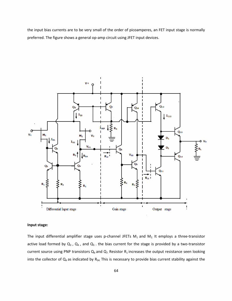
Moreover, as the input bias currents are to be very small of the order of picoamperes, an FET input
stage is normally preferred. The figure shows a general op-amp circuit using JFET input devices.

Input stage:
The input differential amplifier stage uses p-channel JFETs M1 and M2. It employs a three-transistor
active load formed by Q3 , Q4 , and Q5 . the bias current for the stage is provided by a two-transistor
current source using PNP transistors Q6 and Q7. Resistor R1 increases the output resistance seen
looking into the collector of Q4 as indicated by R04. This is necessary to provide bias current
stability against the transistor parameter variations. Resistor R2 establishes a definite bias current
through Q5 . A single ended output is taken out at the collector of Q4 .
MOSFET’s are used in place of JFETs with additional devices in the circuit to prevent any damage
for the gate oxide due to electrostatic discharges.
Gain stage:
The second stage or the gain stage uses Darlington transistor pair formed by Q8 and Q9 as shown in
figure. The transistor Q8 is connected as an emitter follower, providing large input resistance.

Therefore, it minimizes the loading effect on the input differential amplifier stage. The transistor
Q9 provides an additional gain and Q10 acts as an active load for this stage. The current mirror
formed by Q7 and Q10 establishes the bias current for Q9 . The VBE drop across Q9 and drop across R5
constitute the voltage drop across R4 , and this voltage sets the current through Q8 . It can be set to a
small value, such that the base current of Q8 also is very less.
Output stage:
The final stage of the op-amp is a class AB complementary push-pull output stage. Q11 is an emitter
follower, providing a large input resistance for minimizing the loading effects on the gain stage.
Bias current for Q11 is provided by the current mirror formed by Q7 and Q12, through Q13 and Q14 for
minimizing the cross over distortion. Transistors can also be used in place of the two diodes.
The overall voltage gain AV of the op-amp is the product of voltage gain of each stage as given by
AV = |Ad | |A2||A3|
Where Ad is the gain of the differential amplifier stage, A2 is the gain of the second gain stage and
A3 is the gain of the output stage.
IC 741 Bipolar operational amplifier:
The IC 741 produced since 1966 by several manufactures is a widely used general purpose
operational amplifier. Figure shows that equivalent circuit of the 741 op-amp, divided into various
individual stages. The op-amp circuit consists of three stages.
1. the input differential amplifier
2. The gain stage
3. the output stage.
A bias circuit is used to establish the bias current for whole of the circuit in the IC. The op-amp is
supplied with positive and negative supply voltages of value ± 15V, and the supply voltages as low
as ±5V can also be used.
Bias Circuit:
The reference bias current IREF for the 741 circuit is established by the bias circuit consisting of two
diodes-connected transistors Q11 and Q12 and resistor R5. The widlar current source formed by Q11 ,
Q10 and R4 provide bias current for the differential amplifier stage at the collector of Q10. Transistors
Q8 and Q9 form another current mirror providing bias current for the differential amplifier. The

reference bias current IREF also provides mirrored and proportional current at the collector of the
double –collector lateral PNP transistor Q13. The transistor Q13 and Q12 thus form a two-output
current mirror with Q13A providing bias current for output stage and Q13B providing bias current for
Q17. The transistor Q18 and Q19 provide dc bias for the output stage. Formed by Q14 and Q20 and they
establish two VBE drops of potential difference between the bases of Q14 and Q18 .
Input stage:
The input differential amplifier stage consists of transistors Q1 through Q7 with biasing provided by
Q8 through Q12. The transistor Q1 and Q2 form emitter – followers contributing to high
differential input resistance, and whose output currents are inputs to the common base amplifier
using Q3 and Q4 which offers a large voltage gain.
The transistors Q5, Q6 and Q7 along with resistors R1, R2 and R3 from the active load for
input stage. The single-ended output is available at the collector of Q6. the two null terminals in the
input stage facilitate the null adjustment. The lateral PNP transistors Q3 and Q4 provide
additional protection against voltage breakdown conditions. The emitter-base junction Q3 and Q4
have higher emitter-base breakdown voltages of about 50V. Therefore, placing PNP transistors
in series with NPN transistors provide protection against accidental shorting of supply to the input
terminals. Gain Stage:
The Second or the gain stage consists of transistors Q16 and Q17, with Q16 acting as an emitter –
follower for achieving high input resistance. The transistor Q17 operates in common emitter
configuration with its collector voltage applied as input to the output stage. Level shifting is done
for this signal at this stage.
Internal compensation through Miller compensation technique is achieved using the feedback
capacitor C1 connected between the output and input terminals of the gain stage.
Output stage:
The output stage is a class AB circuit consisting of complementary emitter follower transistor pair
Q14 and Q20 . Hence, they provide an effective loss output resistance and current gain.
The output of the gain stage is connected at the base of Q22 , which is connected as an emitter –
follower providing a very high input resistance, and it offers no appreciable loading effect on the

gain stage. It is biased by transistor Q13A which also drives Q18 and Q19, that are used for establishing
a quiescent bias current in the output transistors Q14 and Q20.
Ideal op-amp characteristics:
1. Infinite voltage gain A.
2. Infinite input resistance Ri, so that almost any signal source can drive it and there is no
loading of the proceeding stage.
3. Zero output resistance Ro, so that the output can drive an infinite number of other devices.
4. Zero output voltage, when input voltage is zero.
5. Infinite bandwidth, so that any frequency signals from o to ∞ HZ can be amplified with out
attenuation.
6. Infinite common mode rejection ratio, so that the output common mode noise voltage is
zero.
7. Infinite slew rate, so that output voltage changes occur simultaneously with input voltage
changes.
AC Characteristics:
For small signal sinusoidal (AC) application one has to know the ac characteristics
such as frequency response and slew-rate.
Frequency Response:
The variation in operating frequency will cause variations in gain magnitude and its
phase angle. The manner in which the gain of the op-amp responds to different frequencies is
called the frequency response. Op-amp should have an infinite bandwidth Bw =∞ (i.e) if its open
loop gain in 90dB with dc signal its gain should remain the same 90 dB through audio and onto
high radio frequency. The op-amp gain decreases (roll-off) at higher frequency what reasons to
decrease gain after a certain frequency reached. There must be a capacitive component in the
equivalent circuit of the op-amp. For an op-amp with only one break (corner) frequency all the
capacitors effects can be represented by a single capacitor C. Below fig is a modified variation of
the low frequency model with capacitor C at the o/p.

There is one pole due to R0 C and one -20dB/decade. The open loop voltage gain of an op-amp
with only one corner frequency is obtained from above fig.
f@ fjfX fC
f ` a
A Vd @@@@ 26 V 0
0 @ jX C
V f f f
b fAfOfL f
or A Vd c
1 2j R0 C
` a
or A fAfOf fL f g
f @@@@@ 27
1 j ff f
1
` a
where f f1f f @@@ 28 2 R
0 C
f1 is the corner frequency or the upper 3 dB frequency of the op-amp. The magnitude and phase
angle of the open loop volt gain are fu of frequency can be written as,
L M fA
fOfL f ` a L M v
u u
w f g 2
@@@@@@@ 29
u ff f t
1
h i
@tan@1j ff fk
1
The magnitude and phase angle characteristics from eqn (29) and (30)
1. For frequency f<< f1 the magnitude of the gain is 20 log AOL in dB.
2. At frequency f = f1 the gain in 3 dB down from the dc value of AOL in dB. This frequency f1
is called corner frequency.
3. For f>> f1 the fain roll-off at the rate off -20dB/decade or -6dB/decade.

From the phase characteristics that the phase angle is zero at frequency f =0.
At the corner frequency f1 the phase angle is -450 (lagging and a infinite frequency the phase angle
is -900 . It shows that a maximum of 900 phase change can occur in an op-amp with a single
capacitor C. Zero frequency is taken as te decade below the corner frequency and infinite
frequency is one decade above the corner frequency. The voltage transfer in a S-domain can be
written as
AffOfL f A f g
fAf f f d e
1 j ff f
1
1 j w f w
1
AfOfL f@
fwf1 f AfOfL fAfW
f1 f
A jw w1
S W 1
The transfer f0 of as op-amp with 3 break frequency can be assumed as,

fAfOfL
f 0< f < f < f
` a
@@@@ 31 A f g f g f g 1 2 3
1 j ff f
1
1 j ff f
2
1 j ff f
3
fAfOfL
fwf1ffw
f2 fwf3 f ` a
A ` a a a s w s w s w @@@ 32 with 0<w1 <w2 <w3
1 2 3
Circuit Stability: A circuit or a group of circuit connected together as a system is said to be stable, if its
o/p reaches a fixed value in a finite time. (or) A system is said to be unstable, if its o/p increases
with time instead of achieving a fixed value. In fact the o/p of an unstable sys keeps on increasing
until the system break down. The unstable system are impractical and need be made stable. The
criterian gn for stability is used when the system is to be tested practically. In theoretically, always
used to test system for stability , ex: Bode plots.
Bode plots are compared of magnitude Vs Frequency and phase angle Vs frequency. Any system
whose stability is to be determined can represented by the block diagram.

The block between the output and input is referred to as forward block and the block between the
output signal and f/b signal is referred to as feedback block. The content of each block is referred
“Transfer frequency’ From fig we represented it by AOL (f) which is given by
AOL (f) = V0 /Vin if Vf = 0. -----(1)
where AOL (f) = open loop volt gain. The closed loop gain Af is given by
AF = V0 /Vin
AF = AOL / (1+(AOL ) (B) ----(2)
B = gain of feedback circuit.
B is a constant if the feedback circuit uses only resistive components. Once the magnitude Vs
frequency and phase angle Vs frequency plots are drawn, system stability may be determined as
follows
1. Method:1:
Determine the phase angle when the magnitude of (AOL ) (B) is 0dB (or) 1. If phase angle is > .-
1800 , the system is stable. However, the some systems the magnitude may never be 0, in that cases
method 2, must be used.
2. Method 2:
Determine the phase angle when the magnitude of (AOL ) (B) is 0dB (or) 1. If phase angle is > .-
1800 , If the magnitude is –ve decibels then the system is stable. However, the some systems the
phase angle of a system may reach -1800 , under such conditions method 1 must be used to
determine the system stability.
Slew Rate:
Another important frequency related parameter of an op-amp is the slew rate. (Slew rate is the
maximum rate of change of output voltage with respect to time. Specified in V/μs).
Reason for Slew rate:
There is usually a capacitor within 0, outside an op-amp oscillation. It is this capacitor which
prevents the o/p voltage from fast changing input. The rate at which the volt across the capacitor
increases is given by
dVc/dt = I/C --------(1)
I -> Maximum amount furnished by the op-amp to capacitor C. Op-amp should have the either a
higher current or small compensating capacitors.

For 741 IC, the maximum internal capacitor charging current is limited to about 15μA. So the slew
rate of 741 IC is
SR = dVc/dt |max = Imax/C .
For a sine wave input, the effect of slew rate can be calculated as consider volt follower -> The
input is large amp, high frequency sine wave .
If Vs = Vm Sinwt then output V0 = Vm sinwt . The rate of change of output is given by
dV0/dt = Vm w coswt.
The max rate of change of output across when coswt =1
(i.e) SR = dV0/dt |max = wVm.
SR = 2∏fVm V/s = 2∏fVm v/ms.
Thus the maximum frequency fmax at which we can obtain an undistorted output volt of peak
value Vm is given by
fmax (Hz) = Slew rate/6.28 * Vm .
called the full power response. It is maximum frequency of a large amplitude sine wave with
which op-amp can have without distortion.
DC Characteristics of op-amp:
Current is taken from the source into the op-amp inputs respond differently to current and
voltage due to mismatch in transistor.
DC output voltages are,
1. Input bias current
2. Input offset current
3. Input offset voltage
4. Thermal drift
Input bias current: The op-amp’s input is differential amplifier, which may be made of BJT or FET.
In an ideal op-amp, we assumed that no current is drawn from the input terminals.
The base currents entering into the inverting and non-inverting terminals (I -
respectively).
& I +
Even though both the transistors are identical, IB- and I +
internal imbalance between the two inputs.
Manufacturers specify the input bias current IB
are not exactly equal due to
@
So, I B
I fB fI fB Q
` a
2 If input voltage Vi = 0V. The output Voltage Vo should also be (Vo = 0)
IB = 500nA
We find that the output voltage is offset by,

b c ` a
V o I B R f
Q 2
Op-amp with a 1M feedback resistor
Vo = 5000nA X 1M = 500mV
The output is driven to 500mV with zero input, because of the bias currents.
In application where the signal levels are measured in mV, this is totally unacceptable. This can be
compensated. Where a compensation resistor Rcomp has been added between the non-inverting input
terminal and ground as shown in the figure below.
Current I +
flowing through the compensating resistor Rcomp, then by KVL we get,
-V1+0+V2-Vo = 0 (or)
Vo = V2 – V1 ——>(3)
By selecting proper value of Rcomp, V2 can be cancelled with V1 and the Vo = 0. The value of Rcomp
is derived a
V1 = IB+Rcomp (or)
IB+ = V1/Rcomp ——>(4)
The node ‘a’ is at voltage (-V1). Because the voltage at the non-inverting input terminal is (-V1).
So with Vi = 0 we get,
I1 = V1/R1 ——
>(5) I2 = V2/Rf —
—>(6)
For compensation, Vo should equal to zero (Vo = 0, Vi = 0). i.e. from equation (3) V2 = V1. So
that, I2 = V1/Rf ——>(7)
KCL at node ‘a’ gives,
IB- = I2 + I1
@ V f1
f V f1 f
I B
f 1
b c
@ R 1 R
f f ` a
I B V 1
- +
Q 8 R 1 R
f
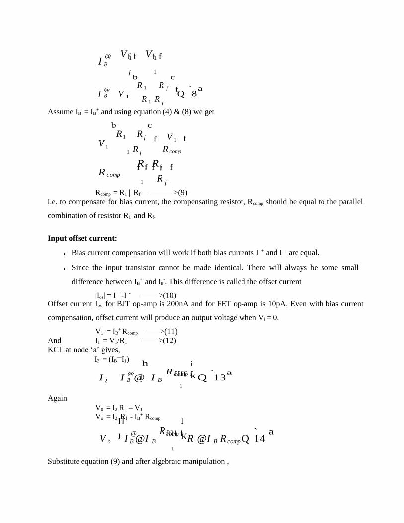
Assume IB = IB and using equation (4) & (8) we get
b c
R 1 R f f
V 1 f
V 1
1 R f
fR f1 fR
R comp
ff f R comp
1 R f
Rcomp = R1 || Rf ———>(9)
i.e. to compensate for bias current, the compensating resistor, Rcomp should be equal to the parallel
combination of resistor R1 and Rf.
Input offset current:
Bias current compensation will work if both bias currents I +
and I -
are equal.
Since the input transistor cannot be made identical. There will always be some small
difference between IB+ and IB
-. This difference is called the offset current
|Ios| = I +-I -
——>(10)
Offset current Ios for BJT op-amp is 200nA and for FET op-amp is 10pA. Even with bias current
compensation, offset current will produce an output voltage when Vi = 0.
V1 = IB+ Rcomp ——>(11)
And I1 = V1/R1 ——>(12)
KCL at node ‘a’ gives, —
I2 = (IB I1) h
@
i
R fcfofmfp f ` a
Again
I 2 I B @j I B
V0 = I2 Rf – V1
k Q 1 3 1
Vo = I2 Rf - IB+ Rcomp
H
@ R
I
fcfofmfp f ` a
V o J I B @I B
KR @I B R comp Q 1 4 1
Substitute equation (9) and after algebraic manipulation ,

H I
@ R fcfofmfp f
V o R f J I B @I B
K@I B R comp
1
V o R fI
@I B
R fcfofmfp
R 1
f @I B R comp
H
@ J R
I
ff f 1K
V o R
f I B @I B R comp
1
H I
@ J R ff fRf f1 fK
V o R f
I B @I B R comp
1
@ R f1 fR
ff f
V o R f
I B @I B
1
V o R f
I B @I B R f
B @
C ` a
V o R f
I B @I B Q 1 5 ` a
V o R f
I os Q 1 6 So even with bias current compensation and with feedback resistor of 1M, a BJT op-amp has an
output offset voltage
Vo = 1M Ω X 200nA
Vo = 200mV with Vi = 0
Equation (16) the offset current can be minimized by keeping feedback resistance small.
Unfortunately to obtain high input impedance, R1 must be kept large.
R1 large, the feedback resistor Rf must also be high. So as to obtain reasonable gain.
The T-feedback network is a good solution. This will allow large feedback resistance, while
keeping the resistance to ground low (in dotted line).
The T-network provides a feedback signal as if the network were a single feedback resistor.
By T to Π conversion,
R ft
f2fR
ft fR
fs f ` a R
f
s
Q 1 7
To design T- network first pick Rt<<Rf/2 ——>(18) 2
fRft
f ` a
Then calculate R s
R f
2 R t Q 1 9

Input offset voltage:
Inspite of the use of the above compensating techniques, it is found that the output voltage
may still not be zero with zero input voltage [Vo ≠ 0 with Vi = 0]. This is due to unavoidable
imbalances inside the op-amp and one may have to apply a small voltage at the input terminal to
make output (Vo) = 0.
This voltage is called input offset voltage Vos. This is the voltage required to be applied at
the input for making output voltage to zero (Vo = 0).

Let us determine the Vos on the output of inverting and non-inverting amplifier. If Vi = 0 (Fig (b)
and (c)) become the same as in figure (d). The voltage V2 at the negative input terminal is given by h i
fRf f1 f ` a
V 2 j
1
k V o Q 2 0 f
(or)
h R f1
i
fR ff f
h i R ff f ` a
V o j
1
L L
k V 2 j 1
M M
k V 2 Q 2 1 1
Since, V os L V i @V 2M& V i 0 L M ` a a
V os L 0 @V 2M V 2 Q 2 2 o r h i
R ff f ` a
V o j 1 k V os Q 2 3
1
Thus, the output offset voltage of an op-amp in closed loop is given by equation (23).
Total output offset voltage:
The total output offset voltage VOT could be either more or less than the offset voltage
produced at the output due to input bias current (IB) or input offset voltage alone(Vos).
This is because IB and Vos could be either positive or negative with respect to
ground. Therefore the maximum offset voltage at the output of an inverting and non-inverting
amplifier (figure b, c) without any compensation technique used is given by many op-amp
provide offset compensation pins to nullify the offset voltage.
10K potentiometer is placed across offset null pins 1&5. The wipes connected to the
negative supply at pin 4.
The position of the wipes is adjusted to nullify the offset voltage.

When the given (below) op-amps does not have these offset null pins, external balancing
techniques are used. H I
R fff f ` a
V OT J 1 KV os R
f I B Q 2 4
1
With Rcomp, the total output offset voltage H I
R ff f ` a
V OT J 1
Balancing circuit:
Inverting amplifier:
KV os R f
I os Q 2 5 1
Non-inverting amplifier:
Thermal drift:
Bias current, offset current, and offset voltage change with temperature.
A circuit carefully nulled at 25ºC may not remain. So when the temperature rises to 35ºC.
This is called drift.
Offset current drift is expressed in nA/ºC.
These indicate the change in offset for each degree Celsius change in temperature.
Open – loop op-amp Configuration:
The term open-loop indicates that no feedback in any form is fed to the input from the output.
When connected in open – loop, the op-amp functions as a very high gain amplifier. There are
three open – loop configurations of op-amp namely,
1. differential amplifier
2. Inverting amplifier
3. Non-inverting amplifier
The above classification is made based on the number of inputs used and the terminal to which
the input is applied. The op-amp amplifies both ac and dc input signals. Thus, the input signals can
be either ac or dc voltage.
Open – loop Differential Amplifier:
In this configuration, the inputs are applied to both the inverting and the non-inverting
input terminals of the op-amp and it amplifies the difference between the two input voltages.
Figure shows the open-loop differential amplifier configuration.
The input voltages are represented by Vi1 and Vi2. The source resistance Ri1 and Ri2 are
negligibly small in comparison with the very high input resistance offered by the op-amp, and thus

the voltage drop across these source resistances is assumed to be zero. The output voltage V0 is
given by
V0 = A(Vi1 – Vi2 )
where A is the large signal voltage gain. Thus the output voltage is equal to the voltage gain A
times the difference between the two input voltages. This is the reason why this configuration is
called a differential amplifier. In open – loop configurations, the large signal voltage gain A is also
called open-loop gain A.
Inverting amplifier:

In this configuration the input signal is applied to the inverting input terminal of the op-
amp and the non-inverting input terminal is connected to the ground. Figure shows the circuit of an
open – loop inverting amplifier.
The output voltage is 1800 out of phase with respect to the input and hence, the output voltage V0 is
given by,
V0 = -AVi
Thus, in an inverting amplifier, the input signal is amplified by the open-loop gain A and in phase
– shifted by 1800.
Non-inverting Amplifier:

Figure shows the open – loop non- inverting amplifier. The input signal is applied to the
non-inverting input terminal of the op-amp and the inverting input terminal is connected to the
ground.
The input signal is amplified by the open – loop gain A and the output is in-phase with input
signal.
V0 = AVi
In all the above open-loop configurations, only very small values of input voltages can be applied.
Even for voltages levels slightly greater than zero, the output is driven into saturation, which is
observed from the ideal transfer characteristics of op-amp shown in figure. Thus, when operated in
the open-loop configuration, the output of the op-amp is either in negative or positive saturation, or
switches between positive and negative saturation levels. This prevents the use of open – loop
configuration of op-amps in linear applications.
Limitations of Open – loop Op – amp configuration:
Firstly, in the open – loop configurations, clipping of the output waveform can occur when the
output voltage exceeds the saturation level of op-amp. This is due to the very high open – loop
gain of the op-amp. This feature actually makes it possible to amplify very low frequency signal of
the order of microvolt or even less, and the amplification can be achieved accurately without any

distortion. However, signals of such magnitudes are susceptible to noise and the amplification for
those application is almost impossible to obtain in the laboratory.
Secondly, the open – loop gain of the op – amp is not a constant and it varies with changing
temperature and variations in power supply. Also, the bandwidth of most of the open- loop op
amps is negligibly small. This makes the open – loop configuration of op-amp unsuitable for ac
applications. The open – loop bandwidth of the widely used 741 IC is approximately 5Hz. But in
almost all ac applications, the bandwidth requirement is much larger than this.
For the reason stated, the open – loop op-amp is generally not used in linear applications.
However, the open – loop op amp configurations find use in certain non – linear applications such
as comparators, square wave generators and astable multivibrators.
Closed – loop op-amp configuration:
The op-amp can be effectively utilized in linear applications by providing a feedback from
the output to the input, either directly or through another network. If the signal feedback is out- of-
phase by 1800 with respect to the input, then the feedback is referred to as negative feedback or
degenerative feedback. Conversely, if the feedback signal is in phase with that at the input, then
the feedback is referred to as positive feedback or regenerative feedback.
An op – amp that uses feedback is called a closed – loop amplifier. The most commonly used
closed – loop amplifier configurations are 1. Inverting amplifier (Voltage shunt amplifier) 2. Non-
Inverting amplifier (Voltage – series Amplifier)
Inverting Amplifier:
The inverting amplifier is shown in figure and its alternate circuit arrangement is shown in
figure, with the circuit redrawn in a different way to illustrate how the voltage shunt feedback is
achieved. The input signal drives the inverting input of the op – amp through resistor R1 .
The op – amp has an open – loop gain of A, so that the output signal is much larger than the error
voltage. Because of the phase inversion, the output signal is 1800 out – of – phase with the input
signal. This means that the feedback signal opposes the input signal and the feedback is negative or
degenerative.
Virtual Ground:

A virtual ground is a ground which acts like a ground . It may not have physical connection to
ground. This property of an ideal op – amp indicates that the inverting and non – inverting
terminals of the op –amp are at the same potential. The non – inverting input is grounded for the
inverting amplifier circuit. This means that the inverting input of the op –amp is also at ground
potential. Therefore, a virtual ground is a point that is at the fixed ground potential (0V), though it
is not practically connected to the actual ground or common terminal of the circuit.
The open – loop gain of an op – amp is extremely high, typically 200,000 for a 741. For ex, when
the output voltage is 10V, the input differential voltage Vid is given by
V id
V f0 f
A
f1f0
200,000
f 0.05mV
Further more, the open – loop input impedance of a 741 is around 2MΩ. Therefore, for an input
differential voltage of 0.05mV, the input current is only
I Vfifd Ri
f 0f.f0f5fmfV
2M
f 0.25nA
Since the input current is so small compared to all other signal currents, it can be approximated as
zero. For any input voltage applied at the inverting input, the input differential voltage V id is
negligibly small and the input current is ideally zero. Hence, the inverting input acts as a virtual
ground. The term virtual ground signifies a point whose voltage with respect to ground is zero, and
yet no current can flow into it.

The expression for the closed – loop voltage gain of an inverting amplifier can be obtained from
figure. Since the inverting input is at virtual ground, the input impedance is the resistance between
the inverting input terminal and the ground. That is, Zi = R1. Therefore, all of the input voltage
appears across R1 and it sets up a current through R1 that equals I 1
Vfif
R1
. The current must flow
through Rf because the virtual ground accepts negligible current. The left end of Rf is ideally
grounded, and hence the output voltage appears wholly across it. Therefore,
R ff f V f0 f
R ff f
V 0 @I 2 R f @ 1
V i . The closed –loop voltage gain AV is given by Av @ . i 1
The input impedance can be set by selecting the input resistor R1 . Moreover, the above equation
shows that the gain of the inverting amplifier is set by selecting a ratio of feedback resistor Rf to
the input resistor R1 . The ratio Rf /R1 can be set to any value less than or greater than unity. This
feature of the gain equation makes the inverting amplifier with feedback very popular and it lends
this configuration to a majority of applications.
Practical Considerations:
1. Setting the input impedance R1 to be too high will pose problems for the bias current, and it
is usually restricted to 10KΩ.
2. The gain cannot be set very high due to the upper limit set by the fain – bandwidth (GBW =
Av * f) product. The Av is normally below 100.
3. The peak output of the op – amp is limited by the power supply voltages, and it is about 2V
less than supply, beyond which, the op – amp enters into saturation.
4. The output current may not be short – circuit limited, and heavy loads may damage the op
– amp. When short – circuit protection is provided, a heavy load may drastically distort the
output voltage.
Practical Inverting amplifier:
The practical inverting amplifier has finite value of input resistance and input current, its
open voltage gain A0 is less than infinity and its output resistance R0 is not zero, as against the
ideal inverting amplifier with finite input resistance, infinite open – loop voltage gain and zero
output resistance respectively.
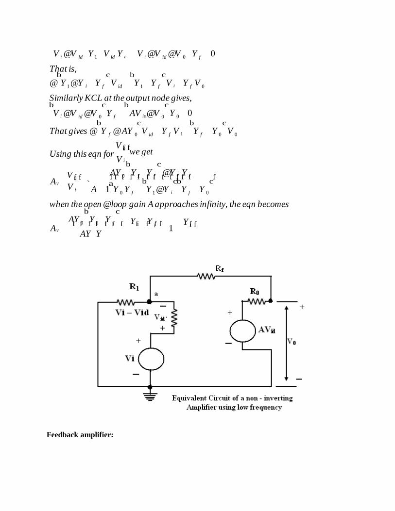
Figure shows the low frequency equivalent circuit model of a practical inverting amplifier. This
circuit can be simplified using the Thevenin’s equivalent circuit shown in figure. The signal source
Vi and the resistors R1 and Ri are replaced by their Thevenin’s equivalent values. The closed – loop
gain AV and the input impedance Rif are calculated as follows.
The input impedance of the op- amp is normally much larger than the input resistance R1.
Therefore, we can assume Veq ≈ Vi and Req ≈ R1 . From the figure we get,
V 0 IR0 AV id
and V id IR f V 0 0
Substituting the value of V id from above eqn , we get, ` a
V 0
1 A b c
I R0 @AR f
Also using the KVL , we get b c
V i I R1 R f V 0
Substituting the value of I derived from above eqn and obtaining the closed
loop gain Av , we get
V f0 f
fRf0 f@
fAf fR ff f
Av
i
R0 R f ` a
R1 1 A
It can be observed from above eqn that when A>> 1, R0 is negligibly small and the product AR1 >>
R0 +Rf , the closed loop gain is given by

R ff f
Av @ 1
Which is as the same form as given in above eqn for an ideal inverter.
Input Resistance:
From figure we get,
Rif
Vfifd f
I 1
Using KVL, we get, b c
V id I 1 R f R0
AV id 0
which can be simplified for Rif as
V fiff f R ff
fRf0 f
Rif 1 A

Output Resistance:
Figure shows the equivalent circuit to determine Rof . The output impedance Rof without the
load resistance factor RL is calculated from the open circuit output voltage Voc and the short
circuit output current ISC . From the figure, when the output is short circuited, we get

I Vfif@f0 f
1 R R 1 f
AfV
fifdf f
and I 0
0
we know that V id @I 1 R f
Therefore, I 0 @ AfIf1 fR
R
ff f
0
The short circuit current is
fRf0f@
fAfRff f
I SC I 1 I 0 V i b c
R0 R1 R f
V fofc f
V fofc f
The output resistance Rof
I sc
and the closed open loop gain Av
i
Therefore,
fA
fvfV fi f
Rof
H
fRf0 f@
I
fAf fR ff f
V iJ b c K
R0
R1
R f
Substituting the v alue of Av from abov e eqn, we get b c
R0
R1
R f
f f a R
of R0
R f
R1
1 A b c
Rf0 f
Rf1 f
Rf ff f
fRf0 fRf1 fR ff f
F G
1 fR f1 fA f
R0
R 1
R f
In the above equation, the numerator contains the term R0 || (R1 +Rf ) and it is smaller than R0 . The
output resistance Rof is therefore always smaller than R0 and from above eqn for Av -> ∞, the
output resistance Rof -> 0.
Non –Inverting Amplifier:

The non – inverting Amplifier with negative feedback is shown in figure. The input signal drives
the non – inverting input of op-amp. The op-amp provides an internal gain A. The external
resistors R1 and Rf form the feedback voltage divider circuit with an attenuation factor of β. Since
the feedback voltage is at the inverting input, it opposes the input voltage at the non – inverting
input terminals, and hence the feedback is negative or degenerative.
The differential voltage Vid at the input of the op-amp is zero, because node a is at the same voltage
as that of the non- inverting input terminal. As shown in figure, Rf and R1 form a potential divider.
Therefore,
fRf1
1 R f
fB V
Since no current flows into the op-amp.
V f0 f Rf1
fR ff f R ff f
Eqn can be written as 1 i f R1
Hence, the voltage gain for the non – inverting amplifier is given by
V f0 f R ff f
AV 1 i 1
Using the alternate circuit arrangement shown in figure, the feedback factor of the feedback
voltage divider network is fRf1 f
R1 R f
1 f Rf1
fR ff f
Av
Therefore, the closed loop – gain is
1
R1
R ff f
R1
From the above eqn, it can be observed that the closed – loop gain is always greater than one and it
depends on the ratio of the feedback resistors. If precision resistors are used in the feedback
network, a precise value of closed – loop gain can be achieved. The closed – loop gain does not
drift with temperature changes or op – amp replacements.

Closed Loop Non – Inverting Amplifier
The input resistance of the op – amp is extremely large (approximately infinity,) since the op –
amp draws negligible current from the input signal.
Practical Non –inverting amplifier:
The equivalent circuit of a non- inverting amplifier using the low frequency model is shown
below in figure. Using Kirchoff’s current law at node a,
V i @V id Y 1 V id Y i V i @V id @V 0 Y f 0
That is, b c
@ Y 1 @Y i Y f b c
V id Y 1 Y f
V i Y f V 0
Similarly KCL at the output node gives, b c
V i @V id @V 0
b c
Y f AV is @V 0
Y 0 0 b c
That gives @ Y f @AY 0
b c
V id Y f V i Y f Y 0 V 0
V
Using this eqn for V
f0 fwe get i b c
V f0 f
fA
fY
f0 fY
f1
fY
ff f@
fY
ff fY
fi f
Av V ` a b cb c
i A 1 Y 0 Y f Y 1 @Y i Y f Y 0
when the open @loop gain A approaches infinity, the eqn becomes b c
AfY
f0 fY
f1
fY
ff
f Yf1
fY ff f Y f1 f
Av AY Y
1
Feedback amplifier:

An op-amp that was feedback is called as feedback amplifier. A feedback amplifier is sometimes
referred to as closed loop amplifier because the feedback forms a closed loop between the input
and output. A closed loop amplifier can be represented by using 2 blocks.
1. One for an op-amp
2. another for an feedback circuit.
There are 4 ways to connect these 2 blocks according to whether volt or current.
1. Voltage Series Feedback
2. Voltage Shunt feedback
3. Current Series Feedback
4. Current shunt Feedback
Voltage series and voltage shunt are important because they are most commonly used.
Voltage Series Feedback Amplifier
Voltage shunt feedback Amplifier

Voltage Series Feedback Amplifier:
Before Proceeding, it is necessary to define some terms.
Voltage gain of the op-amp with a without feedback:
Gain of the feedback circuit are defined as open loop volt gain (or gain without feedback) A = V0 /
Vid
Closed loop volt gain (or gain with feedback) AF = V0 /Vin
Gain of the feedback circuit => B = VF /V0 .
1. Negative feedback:
KVL equation for the input loop is,
Vid = Vin -Vf -----(1)
Vin = input voltage.
Vf = feedback voltage.
Vid = difference input voltage.
The difference volt is equal to the input volt minus the f/b volt. (or) The feedback volt always
opposes the input volt (or out of phase by 1800 with respect to the input voltage) hence the
feedback is said to be negative.
It will be performed by computing
1. Closed loop volt gain
2. Input and output resistance

3. Bandwidth
1. Closed loop volt gain:
The closed loop volt gain is AF = V0 /Vin
V0 = Avid =A(V1 –V2 )
A = large signal voltage gain.
From the above eqn, V0 = A(V1 – V2 )
Refer fig, we see that, V1 = Vin
V2 = Vf = R1 V0
------
R1 +Rf Since Ri >> R1
V0 = AVin - R1 V0
------
R1 +Rf
V0 + A R1 V0 = AVin
------

R1 +Rf
Rearranging, we get,
V f0 f
fAf f A
f R
1
f R
F f
f f f
V in 1 fAfRf f1 f
R1
R F
R1 RF AR1
b c
A R1 RF
V in f
V 0
1
Thus
RF A R1
b c
V f0
f A
f R1
f RF f ` a
AF V
f f f
R R AR @@@ 2 in 1 F
b 1
c
Generally, A is large typically10 5
, b c
AR1 >> R1 RF
b c
and R1 RF AR1
AR1
Thus AF
V f0 f 1
V RfF
R
fIdeal
a
` a @@@@ 3
in 1 ` a
The gain of the feedback circuit B is the ratio of V F and V 0 ,
B V fF V 0
f ` a @@@ 4
B fR
R1
f1 f
RF
Compare eqn 3 and 4 we can conclude
A 1 f
ideala
F B
` a @@@ 5
This means that gain of the f b
fcircuit in the reciprocal of the closed loop volt gain A
In other words for given R1 and RF the values of AF and B are fixed. Eqn (5) is an alternative to eqn
(3)
Finally, the closed loop voltage gain AF can be expressed in terms of open loop gain A and
feedback circuit gain B as follows,
From eqn (2),

A V f0
F in
f A
f R1 f f
R1
RF
f RF f
f
AR1
Rearranging the Eqn A f g
A Rf1 fRfF f
fR
f1
fR
fF f
AF 1
fR F f
fAfRf 1 f
R1
R F
R1
R F
` a
using eqn 4 B V fF f V
0
fRf f1 f
R1
R F
A fA
F 1 AB
f @@
` a
where AF closed loop voltage gain
A open loop voltage gain
B Gain of the F b
circuit

55
AB loop gain

56
UNIT II APPLICATIONS OF OP-AMP
Differential amplifier: The function of a differential amplifier is to amplify the difference between two
signals. The need for differential amplifier arises in many physical measurements where response from
dc to many MHz of frequency is required. This forms the basic input stage of an integrated amplifier.
The basic differential amplifier has the following important properties of
1. Excellent stability
2. High versatility and
3. High immunity to interference signals
The differential amplifier as a building block of the op-amp has the advantages of
1. Lower cost
2. easier fabrication as IC component and
3. closely matched components.
The above figure shows the basic block diagram of a differential amplifier, with two input
terminals and one output terminal. The output signal of the differential amplifier is proportional to the
difference between the two input signals.
That is V0 = Adm (V1 – V2 )
If V1 = V2 , then the output voltage is zero. A non-zero output voltage V0 is obtained when V1 and V2 are
not equal. The difference mode input voltage is defined as Vm = V1 – V2 and the common mode input
voltage is defined as

57
These equation show that if V1 = V2 , then the differential mode input signal is zero and common mode
input signal is Vcm = V1 =V2 .
Differential Amplifier with Active load:
Differential amplifier are designed with active loads to increase the differential mode voltage
gain.
The open circuit voltage gain of an op-amp is needed to be as large as possible. This is achieved by
cascading the gain stages which increase the phase shift and the amplifier also becomes vulnerable to
oscillations. The gain can be increased by using large values of collector resistance. For such a circuit.
To increase the gain the IC RC product must be made very large. However, there are limitations in IC
fabrication such as,
1. a large value of resistance needs a large chip area.
2. for large RC, the quiescent drop across the resistor increase and a large power supply will be
required to maintain a given operating current.
3. Large monolithic resistor introduces large parasitic capacitances which limits the frequency
response of the amplifier.
4. for linear operation of the differential pair, the devices should not be allowed to enter into
saturation. This limits the max input voltage that can be applied to the bases of transistors Q1
and Q2 the base-collector junction must be allowed to become forward-biased by more than 0.5
V. The large value of load resistance produces a large dc voltage drop (IEE / 2)RC, so that the
collector voltage will be VC = Vcc -(IEE / 2)RC and it will be substantially less than the supply
voltage Vcc. This will reduce the input voltage range of the differential amplifier. Due to the
reasons cited above, an active load is preferred in the differential amplifier configurations.
BJT Differential Amplifier using active loads:
A simple active load circuit for a differential amplifier is the current mirror active load as shown
in figure. The active load comprises of transistors Q3 and Q4 with the transistor Q3 connected as a diode
with its base and collector shorted. The circuit is shown to drive a load RL. When an ac input voltage is
applied to the differential amplifier . Where IC4 IC3due to current mirror action. We know that the

58
load current IL entering the next stage is therefore. The differential amplifier can amplify the differential
input signals and it provides single-ended output with a ground reference since the load RL is connected
to only one output terminal. This is made possible by the use of the current mirror active load.The
output resistance R0 of the circuit is that offered by the parallel combination of transistors Q2 (NPN) and
Q4 (PNP). It is given by Rr = r02 || r04
59
The voltage gain of the differential amplifier is independent of the quiescent current IEE. This
makes it possible to use very small value of IEE as low as 20μa, while still maintaining a large voltage gain.
Small value of IEE is preferred, since it results in a small value of bias current and a large value for the
input resistance. A limitation in choosing a small IEE is, however, the fact that, it will result in a poor
frequency response of the amplifier.
When a small value of bias current is required, the best approach is to use a JFET or MOSFET
differential amplifier that is operated at comparatively higher values of IEE.

60
Differential Mode signal analysis:
The ac analysis of the differential amplifier can be made using the circuit model as shown below.
The differential input transistor pair produces equal and opposite currents whose amplitude us given by
gm2 Vid /2 at the collector of Q1 and Q2 . The collector current ic1 is fed by the transistor Q3 and it is
mirrored at the output of Q4. Therefore, the total current i0 flowing through the load resistor RL is given
by
This current mirror provides a single ended output which has a voltage equal to the maximum
gain of the common emitter amplifier.

61
The power of the current mirror can be increased by including additional common collector stages at the
o/p of the differential input stage. A bipolar differential amplifier structure with additional stages is
shown in figure. The resistance at the output of the differential stage is now given by the parallel
combination of transistors Q2 and Q4 and the input resistance is offered by Q5. Then, the equivalent
resistance is expressed by Req = ro2 || r04 || ri5 = ri5 . The gain of the differential stage then becomes
Adm gm2 Req gm2 ri5 05
I C2
I C5
fffffff .

62
Bipolar differential amplifier with common mode input signals:
The common mode input signal induces a common mode current iic in each of the differential transistor
pair Q1 and Q2 . The current flow through the transistor Q1 is supplied by the reference current of
transistor Q3. This current is replicated or mirrored in the transistor Q4 and it produces exactly the same
current needed at the collector of Q2. Therefore, the output current and hence the output voltage and
common mode conversion gain Acd are all zero.
However, for an actual amplifier, the common mode gain is determined by small imbalances generated
in the bipolar transistor fabrication and the overall asymmetry in the amplifier. One of the main factors
is due to the current gain defect on the active load, and it can be minimized through the use of buffered
current mirror using the transistor Q5 as shown in figure.

63
General Operational Amplifier:
An operational amplifier generally consists of three stages, anmely,1. a differential amplifier 2.
additional amplifier stages to provide the required voltage gain and dc level shifting 3. an emitter-
follower or source follower output stage to provide current gain and low output resistance.
A low-frequency or dc gain of approximately 104 is desired for a general purpose op-amp and
hence, the use of active load is preferred in the internal circuitry of op-amp. The output voltage is
required to be at ground, when the differential input voltages is zero, and this necessitates the use of
dual polarity supply voltage. Since the output resistance of op-amp is required to be low, a
complementary push-pull emitter – follower or source follower output stage is employed. Moreover, as
64
the input bias currents are to be very small of the order of picoamperes, an FET input stage is normally
preferred. The figure shows a general op-amp circuit using JFET input devices.
Input stage:
The input differential amplifier stage uses p-channel JFETs M1 and M2. It employs a three-transistor
active load formed by Q3 , Q4 , and Q5 . the bias current for the stage is provided by a two-transistor
current source using PNP transistors Q6 and Q7. Resistor R1 increases the output resistance seen looking
into the collector of Q4 as indicated by R04. This is necessary to provide bias current stability against the
65
transistor parameter variations. Resistor R2 establishes a definite bias current through Q5 . A single
ended output is taken out at the collector of Q4 .
MOSFET’s are used in place of JFETs with additional devices in the circuit to prevent any damage for the
gate oxide due to electrostatic discharges.
Gain stage:
The second stage or the gain stage uses Darlington transistor pair formed by Q8 and Q9 as shown in
figure. The transistor Q8 is connected as an emitter follower, providing large input resistance. Therefore,
it minimizes the loading effect on the input differential amplifier stage. The transistor Q9 provides an
additional gain and Q10 acts as an active load for this stage. The current mirror formed by Q7 and Q10
establishes the bias current for Q9 . The VBE drop across Q9 and drop across R5 constitute the voltage drop
across R4 , and this voltage sets the current through Q8 . It can be set to a small value, such that the base
current of Q8 also is very less.
Output stage:
The final stage of the op-amp is a class AB complementary push-pull output stage. Q11 is an emitter
follower, providing a large input resistance for minimizing the loading effects on the gain stage. Bias
current for Q11 is provided by the current mirror formed by Q7 and Q12, through Q13 and Q14 for
minimizing the cross over distortion. Transistors can also be used in place of the two diodes.
The overall voltage gain AV of the op-amp is the product of voltage gain of each stage as given by
AV = |Ad | |A2||A3|
Where Ad is the gain of the differential amplifier stage, A2 is the gain of the second gain stage and A3 is
the gain of the output stage.
IC 741 Bipolar operational amplifier:
The IC 741 produced since 1966 by several manufactures is a widely used general purpose
operational amplifier. Figure shows that equivalent circuit of the 741 op-amp, divided into various
individual stages. The op-amp circuit consists of three stages.

66
1. the input differential amplifier
2. The gain stage
3. the output stage.
A bias circuit is used to establish the bias current for whole of the circuit in the IC. The op-amp is
supplied with positive and negative supply voltages of value ± 15V, and the supply voltages as low as
±5V can also be used.
Bias Circuit:
The reference bias current IREF for the 741 circuit is established by the bias circuit consisting of two
diodes-connected transistors Q11 and Q12 and resistor R5. The widlar current source formed by Q11 , Q10
and R4 provide bias current for the differential amplifier stage at the collector of Q10. Transistors Q8 and
Q9 form another current mirror providing bias current for the differential amplifier. The reference bias
current IREF also provides mirrored and proportional current at the collector of the double –collector
lateral PNP transistor Q13. The transistor Q13 and Q12 thus form a two-output current mirror with Q13A
providing bias current for output stage and Q13B providing bias current for Q17. The transistor Q18 and Q19
provide dc bias for the output stage. Formed by Q14 and Q20 and they establish two VBE drops of potential
difference between the bases of Q14 and Q18 .
Input stage:
The input differential amplifier stage consists of transistors Q1 through Q7 with biasing provided by Q8
through Q12. The transistor Q1 and Q2 form emitter – followers contributing to high differential input
resistance, and whose output currents are inputs to the common base amplifier using Q3 and Q4 which
offers a large voltage gain.
The transistors Q5, Q6 and Q7 along with resistors R1, R2 and R3 from the active load for input stage. The
single-ended output is available at the collector of Q6. the two null terminals in the input stage facilitate
the null adjustment. The lateral PNP transistors Q3 and Q4 provide additional protection against voltage
breakdown conditions. The emitter-base junction Q3 and Q4 have higher emitter-base breakdown
voltages of about 50V. Therefore, placing PNP transistors in series with NPN transistors provide
protection against accidental shorting of supply to the input terminals.

67
Gain Stage:
The Second or the gain stage consists of transistors Q16 and Q17, with Q16 acting as an emitter –follower
for achieving high input resistance. The transistor Q17 operates in common emitter configuration with its
collector voltage applied as input to the output stage. Level shifting is done for this signal at this stage.
Internal compensation through Miller compensation technique is achieved using the feedback capacitor
C1 connected between the output and input terminals of the gain stage.
Output stage:
The output stage is a class AB circuit consisting of complementary emitter follower transistor pair Q14
and Q20 . Hence, they provide an effective loss output resistance and current gain.
The output of the gain stage is connected at the base of Q22 , which is connected as an emitter – follower
providing a very high input resistance, and it offers no appreciable loading effect on the gain stage. It is
biased by transistor Q13A which also drives Q18 and Q19, that are used for establishing a quiescent bias
current in the output transistors Q14 and Q20.
Ideal op-amp characteristics:
1. Infinite voltage gain A.
2. Infinite input resistance Ri, so that almost any signal source can drive it and there is no loading
of the proceeding stage.
3. Zero output resistance Ro, so that the output can drive an infinite number of other devices.
4. Zero output voltage, when input voltage is zero.
5. Infinite bandwidth, so that any frequency signals from o to ∞ HZ can be amplified with out
attenuation.
6. Infinite common mode rejection ratio, so that the output common mode noise voltage is zero.
7. Infinite slew rate, so that output voltage changes occur simultaneously with input voltage
changes.
AC Characteristics:
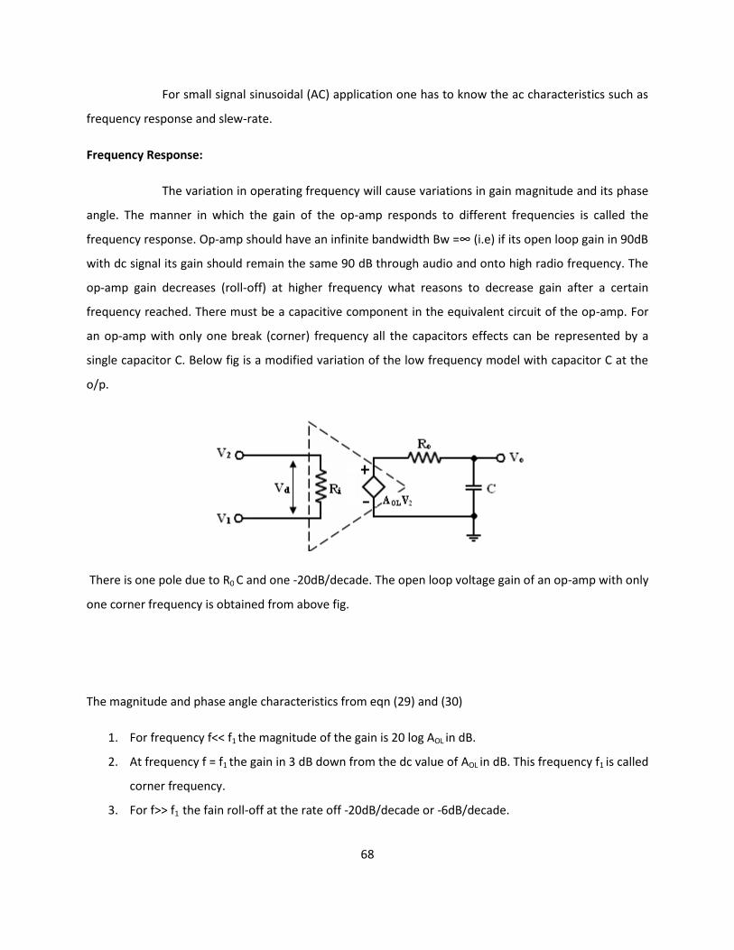
68
For small signal sinusoidal (AC) application one has to know the ac characteristics such as
frequency response and slew-rate.
Frequency Response:
The variation in operating frequency will cause variations in gain magnitude and its phase
angle. The manner in which the gain of the op-amp responds to different frequencies is called the
frequency response. Op-amp should have an infinite bandwidth Bw =∞ (i.e) if its open loop gain in 90dB
with dc signal its gain should remain the same 90 dB through audio and onto high radio frequency. The
op-amp gain decreases (roll-off) at higher frequency what reasons to decrease gain after a certain
frequency reached. There must be a capacitive component in the equivalent circuit of the op-amp. For
an op-amp with only one break (corner) frequency all the capacitors effects can be represented by a
single capacitor C. Below fig is a modified variation of the low frequency model with capacitor C at the
o/p.
There is one pole due to R0 C and one -20dB/decade. The open loop voltage gain of an op-amp with only
one corner frequency is obtained from above fig.
The magnitude and phase angle characteristics from eqn (29) and (30)
1. For frequency f<< f1 the magnitude of the gain is 20 log AOL in dB.
2. At frequency f = f1 the gain in 3 dB down from the dc value of AOL in dB. This frequency f1 is called
corner frequency.
3. For f>> f1 the fain roll-off at the rate off -20dB/decade or -6dB/decade.

69
From the phase characteristics that the phase angle is zero at frequency f =0.
At the corner frequency f1 the phase angle is -450 (lagging and a infinite frequency the phase angle is -900
. It shows that a maximum of 900 phase change can occur in an op-amp with a single capacitor C. Zero
frequency is taken as te decade below the corner frequency and infinite frequency is one decade above
the corner frequency.

70
Circuit Stability:
A circuit or a group of circuit connected together as a system is said to be stable, if its o/p
reaches a fixed value in a finite time. (or) A system is said to be unstable, if its o/p increases with time
instead of achieving a fixed value. In fact the o/p of an unstable sys keeps on increasing until the system
break down. The unstable system are impractical and need be made stable. The criterian gn for stability
is used when the system is to be tested practically. In theoretically, always used to test system for
stability , ex: Bode plots.
Bode plots are compared of magnitude Vs Frequency and phase angle Vs frequency. Any system whose
stability is to be determined can represented by the block diagram.
71
The block between the output and input is referred to as forward block and the block between the
output signal and f/b signal is referred to as feedback block. The content of each block is referred
“Transfer frequency’ From fig we represented it by AOL (f) which is given by
AOL (f) = V0 /Vin if Vf = 0. -----(1)
where AOL (f) = open loop volt gain. The closed loop gain Af is given by
AF = V0 /Vin
AF = AOL / (1+(AOL ) (B) ----(2)
B = gain of feedback circuit.
B is a constant if the feedback circuit uses only resistive components. Once the magnitude Vs frequency
and phase angle Vs frequency plots are drawn, system stability may be determined as follows
1. Method:1:
Determine the phase angle when the magnitude of (AOL ) (B) is 0dB (or) 1. If phase angle is > .-1800 , the
system is stable. However, the some systems the magnitude may never be 0, in that cases method 2,
must be used.
2. Method 2:
Determine the phase angle when the magnitude of (AOL ) (B) is 0dB (or) 1. If phase angle is > .-1800 , If the
magnitude is –ve decibels then the system is stable. However, the some systems the phase angle of a
system may reach -1800 , under such conditions method 1 must be used to determine the system
stability.
Slew Rate:
Another important frequency related parameter of an op-amp is the slew rate. (Slew rate is the
maximum rate of change of output voltage with respect to time. Specified in V/μs).
Reason for Slew rate:

72
There is usually a capacitor within 0, outside an op-amp oscillation. It is this capacitor which prevents
the o/p voltage from fast changing input. The rate at which the volt across the capacitor increases is
given by
dVc/dt = I/C --------(1)
I -> Maximum amount furnished by the op-amp to capacitor C. Op-amp should have the either a higher
current or small compensating capacitors.
For 741 IC, the maximum internal capacitor charging current is limited to about 15μA. So the slew rate
of 741 IC is
SR = dVc/dt |max = Imax/C .
For a sine wave input, the effect of slew rate can be calculated as consider volt follower -> The input is
large amp, high frequency sine wave .
If Vs = Vm Sinwt then output V0 = Vm sinwt . The rate of change of output is given by
dV0/dt = Vm w coswt.
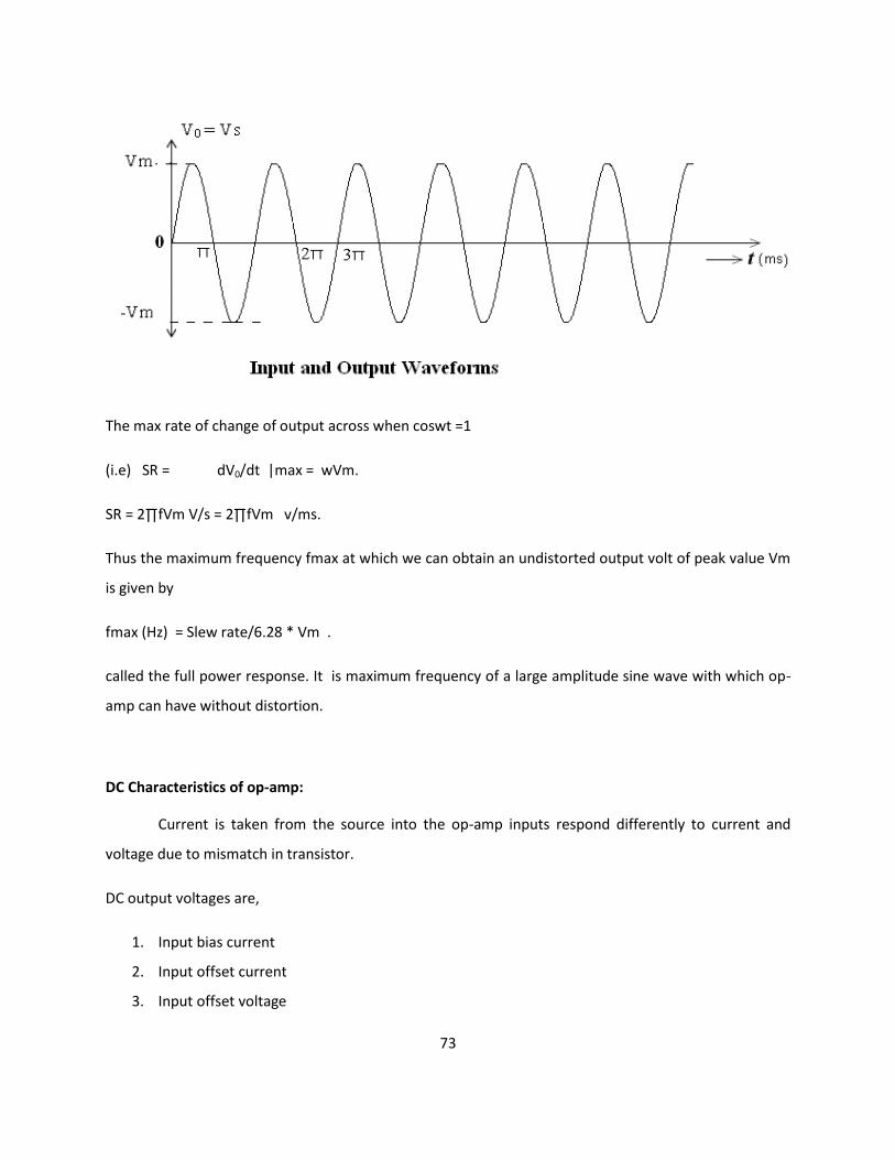
73
The max rate of change of output across when coswt =1
(i.e) SR = dV0/dt |max = wVm.
SR = 2∏fVm V/s = 2∏fVm v/ms.
Thus the maximum frequency fmax at which we can obtain an undistorted output volt of peak value Vm
is given by
fmax (Hz) = Slew rate/6.28 * Vm .
called the full power response. It is maximum frequency of a large amplitude sine wave with which op-
amp can have without distortion.
DC Characteristics of op-amp:
Current is taken from the source into the op-amp inputs respond differently to current and
voltage due to mismatch in transistor.
DC output voltages are,
1. Input bias current
2. Input offset current
3. Input offset voltage
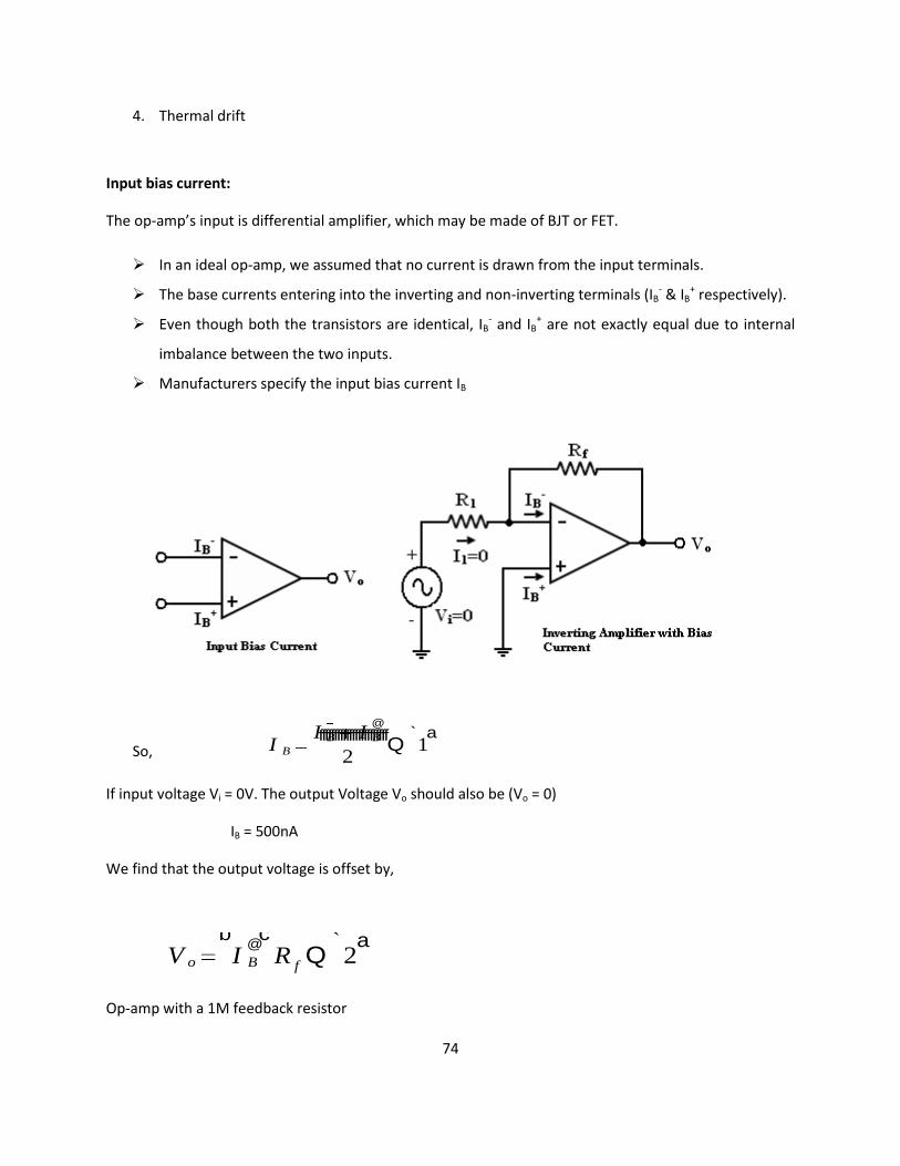
74
4. Thermal drift
Input bias current:
The op-amp’s input is differential amplifier, which may be made of BJT or FET.
In an ideal op-amp, we assumed that no current is drawn from the input terminals.
The base currents entering into the inverting and non-inverting terminals (IB- & IB
+ respectively).
Even though both the transistors are identical, IB- and IB
+ are not exactly equal due to internal
imbalance between the two inputs.
Manufacturers specify the input bias current IB
So, I B
I B I B
@
2
fffffffffffffffffffffffQ 1
` a
If input voltage Vi = 0V. The output Voltage Vo should also be (Vo = 0)
IB = 500nA
We find that the output voltage is offset by,
V o I B
@b c
RfQ 2
` a
Op-amp with a 1M feedback resistor

75
Vo = 5000nA X 1M = 500mV
The output is driven to 500mV with zero input, because of the bias currents.
In application where the signal levels are measured in mV, this is totally unacceptable. This can be
compensated. Where a compensation resistor Rcomp has been added between the non-inverting input
terminal and ground as shown in the figure below.
Current IB+ flowing through the compensating resistor Rcomp, then by KVL we get,
-V1+0+V2-Vo = 0 (or)
Vo = V2 – V1 ——>(3)
By selecting proper value of Rcomp, V2 can be cancelled with V1 and the Vo = 0. The value of Rcomp is
derived a
V1 = IB+Rcomp (or)
IB+ = V1/Rcomp ——>(4)
The node ‘a’ is at voltage (-V1). Because the voltage at the non-inverting input terminal is (-V1). So with
Vi = 0 we get,
I1 = V1/R1 ——>(5)
I2 = V2/Rf ——>(6)
For compensation, Vo should equal to zero (Vo = 0, Vi = 0). i.e. from equation (3) V2 = V1. So that,
76
I2 = V1/Rf ——>(7)
Input offset current:
Bias current compensation will work if both bias currents IB+ and IB
- are equal.
Since the input transistor cannot be made identical. There will always be some small difference
between IB+ and IB
-. This difference is called the offset current
|Ios| = IB+-IB
- ——>(8)
Offset current Ios for BJT op-amp is 200nA and for FET op-amp is 10pA. Even with bias current
compensation, offset current will produce an output voltage when Vi = 0.
V1 = IB+ Rcomp ——>(9)
And I1 = V1/R1 ——>(10)
KCL at node ‘a’ gives,
I2 = (IB—I1)
I 2 I B
@@ I B
R comp
R 1
ffffffffffffff
h
j
i
k Q 13` a
Again
V0 = I2 Rf – V1
Vo = I2 Rf - IB+ Rcomp
V o I B
@@I B
R comp
R 1
ffffffffffffff
H
J
I
KRf@I B R comp Q 14
` a
Substitute equation (9) and after algebraic manipulation ,
So even with bias current compensation and with feedback resistor of 1M, a BJT op-
amp has an output offset voltage
Vo = 1M Ω X 200nA

77
Vo = 200mV with Vi = 0
Equation (16) the offset current can be minimized by keeping feedback resistance small.
Unfortunately to obtain high input impedance, R1 must be kept large.
R1 large, the feedback resistor Rf must also be high. So as to obtain reasonable gain.
The T-feedback network is a good solution. This will allow large feedback resistance, while keeping the
resistance to ground low (in dotted line).
The T-network provides a feedback signal as if the network were a single feedback resistor.
By T to Π conversion,
To design T- network first pick Rt<<Rf/2
Input offset voltage:
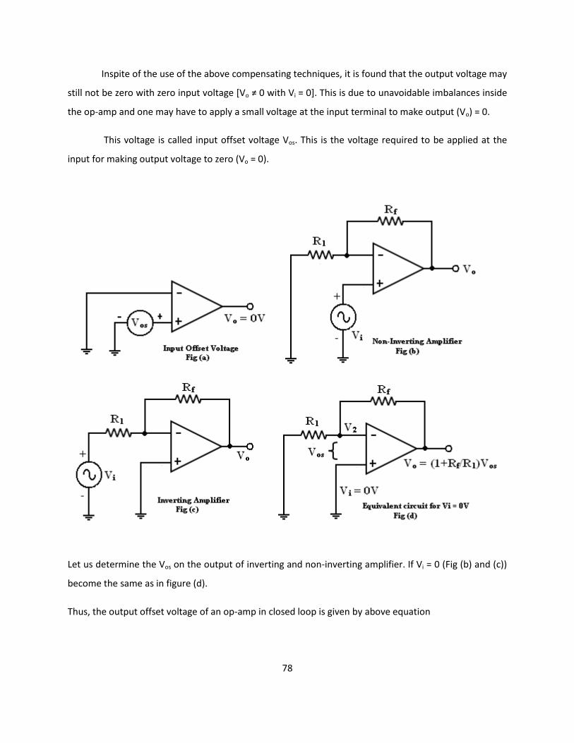
78
Inspite of the use of the above compensating techniques, it is found that the output voltage may
still not be zero with zero input voltage [Vo ≠ 0 with Vi = 0]. This is due to unavoidable imbalances inside
the op-amp and one may have to apply a small voltage at the input terminal to make output (Vo) = 0.
This voltage is called input offset voltage Vos. This is the voltage required to be applied at the
input for making output voltage to zero (Vo = 0).
Let us determine the Vos on the output of inverting and non-inverting amplifier. If Vi = 0 (Fig (b) and (c))
become the same as in figure (d).
Thus, the output offset voltage of an op-amp in closed loop is given by above equation

79
Total output offset voltage:
The total output offset voltage VOT could be either more or less than the offset voltage produced
at the output due to input bias current (IB) or input offset voltage alone(Vos).
This is because IB and Vos could be either positive or negative with respect to ground. Therefore the
maximum offset voltage at the output of an inverting and non-inverting amplifier (figure b, c) without
any compensation technique used is given by many op-amp provide offset compensation pins to nullify
the offset voltage.
10K potentiometer is placed across offset null pins 1&5. The wipes connected to the negative
supply at pin 4.
The position of the wipes is adjusted to nullify the offset voltage.
When the given (below) op-amps does not have these offset null pins, external balancing techniques are
used.
With Rcomp, the total output offset voltage
Inverting amplifier:

80
Non-inverting amplifier:
Thermal drift:
Bias current, offset current, and offset voltage change with temperature.
A circuit carefully nulled at 25ºC may not remain. So when the temperature rises to 35ºC. This is
called drift.
Offset current drift is expressed in nA/ºC.
These indicate the change in offset for each degree Celsius change in temperature.
Open – loop op-amp Configuration:
81
The term open-loop indicates that no feedback in any form is fed to the input from the output.
When connected in open – loop, the op-amp functions as a very high gain amplifier. There are three
open – loop configurations of op-amp namely,
1. differential amplifier
2. Inverting amplifier
3. Non-inverting amplifier
The above classification is made based on the number of inputs used and the terminal to which the
input is applied. The op-amp amplifies both ac and dc input signals. Thus, the input signals can be either
ac or dc voltage.
Open – loop Differential Amplifier:
In this configuration, the inputs are applied to both the inverting and the non-inverting input
terminals of the op-amp and it amplifies the difference between the two input voltages. Figure shows
the open-loop differential amplifier configuration.
The input voltages are represented by Vi1 and Vi2. The source resistance Ri1 and Ri2 are negligibly
small in comparison with the very high input resistance offered by the op-amp, and thus the voltage
drop across these source resistances is assumed to be zero. The output voltage V0 is given by
V0 = A(Vi1 – Vi2 )
where A is the large signal voltage gain. Thus the output voltage is equal to the voltage gain A times the
difference between the two input voltages. This is the reason why this configuration is called a
differential amplifier. In open – loop configurations, the large signal voltage gain A is also called open-
loop gain A.

82
Inverting amplifier:

83
In this configuration the input signal is applied to the inverting input terminal of the op-amp and
the non-inverting input terminal is connected to the ground. Figure shows the circuit of an open – loop
inverting amplifier.
The output voltage is 1800 out of phase with respect to the input and hence, the output voltage V0 is
given by,
V0 = -AVi
Thus, in an inverting amplifier, the input signal is amplified by the open-loop gain A and in phase –
shifted by 1800.
Non-inverting Amplifier:
Figure shows the open – loop non- inverting amplifier. The input signal is applied to the non-
inverting input terminal of the op-amp and the inverting input terminal is connected to the ground.
The input signal is amplified by the open – loop gain A and the output is in-phase with input signal.
V0 = AVi
In all the above open-loop configurations, only very small values of input voltages can be applied. Even
for voltages levels slightly greater than zero, the output is driven into saturation, which is observed from

84
the ideal transfer characteristics of op-amp shown in figure. Thus, when operated in the open-loop
configuration, the output of the op-amp is either in negative or positive saturation, or switches between
positive and negative saturation levels. This prevents the use of open – loop configuration of op-amps in
linear applications.
Limitations of Open – loop Op – amp configuration:
Firstly, in the open – loop configurations, clipping of the output waveform can occur when the output
voltage exceeds the saturation level of op-amp. This is due to the very high open – loop gain of the op-
amp. This feature actually makes it possible to amplify very low frequency signal of the order of
microvolt or even less, and the amplification can be achieved accurately without any distortion.
However, signals of such magnitudes are susceptible to noise and the amplification for those application
is almost impossible to obtain in the laboratory.
Secondly, the open – loop gain of the op – amp is not a constant and it varies with changing
temperature and variations in power supply. Also, the bandwidth of most of the open- loop op amps is
negligibly small. This makes the open – loop configuration of op-amp unsuitable for ac applications. The
open – loop bandwidth of the widely used 741 IC is approximately 5Hz. But in almost all ac applications,
the bandwidth requirement is much larger than this.
For the reason stated, the open – loop op-amp is generally not used in linear applications. However, the
open – loop op amp configurations find use in certain non – linear applications such as comparators,
square wave generators and astable multivibrators.
Closed – loop op-amp configuration:
The op-amp can be effectively utilized in linear applications by providing a feedback from the
output to the input, either directly or through another network. If the signal feedback is out- of- phase
by 1800 with respect to the input, then the feedback is referred to as negative feedback or degenerative
feedback. Conversely, if the feedback signal is in phase with that at the input, then the feedback is
referred to as positive feedback or regenerative feedback.
An op – amp that uses feedback is called a closed – loop amplifier. The most commonly used closed –
loop amplifier configurations are 1. Inverting amplifier (Voltage shunt amplifier) 2. Non- Inverting
amplifier (Voltage – series Amplifier)

85
Inverting Amplifier:
The inverting amplifier is shown in figure and its alternate circuit arrangement is shown in
figure, with the circuit redrawn in a different way to illustrate how the voltage shunt feedback is
achieved. The input signal drives the inverting input of the op – amp through resistor R1 .
The op – amp has an open – loop gain of A, so that the output signal is much larger than the error
voltage. Because of the phase inversion, the output signal is 1800 out – of – phase with the input signal.
This means that the feedback signal opposes the input signal and the feedback is negative or
degenerative.
Virtual Ground:
A virtual ground is a ground which acts like a ground . It may not have physical connection to ground.
This property of an ideal op – amp indicates that the inverting and non – inverting terminals of the op –
amp are at the same potential. The non – inverting input is grounded for the inverting amplifier circuit.
This means that the inverting input of the op –amp is also at ground potential. Therefore, a virtual
ground is a point that is at the fixed ground potential (0V), though it is not practically connected to the
actual ground or common terminal of the circuit.
The open – loop gain of an op – amp is extremely high, typically 200,000 for a 741. For ex, when the
output voltage is 10V, the input differential voltage Vid is given by
V id
V 0
A
fffffff 10
200,000
ffffffffffffffffffff0.05mV
Further more, the open – loop input impedance of a 741 is around 2MΩ. Therefore, for an input
differential voltage of 0.05mV, the input current is only
I i
V id
Ri
ffffffff 0.05mV
2M
fffffffffffffffffffff0.25nAA
Since the input current is so small compared to all other signal currents, it can be approximated as zero.
For any input voltage applied at the inverting input, the input differential voltage Vid is negligibly small
and the input current is ideally zero. Hence, the inverting input acts as a virtual ground. The term virtual
ground signifies a point whose voltage with respect to ground is zero, and yet no current can flow into it.

86
The expression for the closed – loop voltage gain of an inverting amplifier can be obtained from figure.
Since the inverting input is at virtual ground, the input impedance is the resistance between the
inverting input terminal and the ground. That is, Zi = R1. Therefore, all of the input voltage appears across
R1 and it sets up a current through R1 that equals I 1
V i
R1
ffffff . The current must flow through Rf because
the virtual ground accepts negligible current. The left end of Rf is ideally grounded, and hence the output
voltage appears wholly across it. Therefore, V 0 @I 2 R f @R f
R1
fffffffV i . The closed –loop voltage gain
AV is given by Av
V 0
V i
fffffff@
R f
R1
fffffff .
The input impedance can be set by selecting the input resistor R1 . Moreover, the above equation shows
that the gain of the inverting amplifier is set by selecting a ratio of feedback resistor Rf to the input

87
resistor R1 . The ratio Rf /R1 can be set to any value less than or greater than unity. This feature of the
gain equation makes the inverting amplifier with feedback very popular and it lends this configuration to
a majority of applications.
Practical Considerations:
1. Setting the input impedance R1 to be too high will pose problems for the bias current, and it is
usually restricted to 10KΩ.
2. The gain cannot be set very high due to the upper limit set by the fain – bandwidth (GBW = Av *
f) product. The Av is normally below 100.
3. The peak output of the op – amp is limited by the power supply voltages, and it is about 2V less
than supply, beyond which, the op – amp enters into saturation.
4. The output current may not be short – circuit limited, and heavy loads may damage the op –
amp. When short – circuit protection is provided, a heavy load may drastically distort the output
voltage.
Practical Inverting amplifier:
The practical inverting amplifier has finite value of input resistance and input current, its open
voltage gain A0 is less than infinity and its output resistance R0 is not zero, as against the ideal inverting
amplifier with finite input resistance, infinite open – loop voltage gain and zero output resistance
respectively.
Figure shows the low frequency equivalent circuit model of a practical inverting amplifier. This circuit
can be simplified using the Thevenin’s equivalent circuit shown in figure. The signal source Vi and the
resistors R1 and Ri are replaced by their Thevenin’s equivalent values. The closed – loop gain AV and the
input impedance Rif are calculated as follows.
The input impedance of the op- amp is normally much larger than the input resistance R1. Therefore, we
can assume Veq ≈ Vi and Req ≈ R1 . From the figure we get,

88
V 0 IR0 AV id
andV id IR f V 0 0
Substituting the value ofV id from above eqn , we get,
V 0 1 A` a
I R0 @AR f
b c
Also using the KVL , we get
V i I R1 R f
b cV 0
Substituting the value of I derived from above eqn and obtaining the closed
loop gain Av , we get
Av
V 0
V i
fffffff R0 @AR f
R0 R f R1 1 A` a
ffffffffffffffffffffffffffffffffffffffffffffffff
It can be observed from above eqn that when A>> 1, R0 is negligibly small and the product AR1 >> R0 +Rf ,
the closed loop gain is given by
Av @R f
R1
fffffff
Which is as the same form as given in above eqn for an ideal inverter.
Input Resistance:

89
From figure we get,
Rif
V id
I 1
ffffffff
Using KVL, we get,
V id I 1 R f R0
b cAV id 0
which can be simplified for Rif as
Rif
V if
I 1
ffffffff R f R0
1 A
fffffffffffffffffff
Output Resistance:

90
Figure shows the equivalent circuit to determine Rof . The output impedance Rof without the load
resistance factor RL is calculated from the open circuit output voltage Voc and the short circuit output
current ISC . From the figure, when the output is short circuited, we get
In the above equation, the numerator contains the term R0 || (R1 +Rf ) and it is smaller than R0 . The
output resistance Rof is therefore always smaller than R0 and from above eqn for Av -> ∞, the output
resistance Rof -> 0.
Non –Inverting Amplifier:

91
The non – inverting Amplifier with negative feedback is shown in figure. The input signal drives the non
– inverting input of op-amp. The op-amp provides an internal gain A. The external resistors R1 and Rf
form the feedback voltage divider circuit with an attenuation factor of β. Since the feedback voltage is at
the inverting input, it opposes the input voltage at the non – inverting input terminals, and hence the
feedback is negative or degenerative.
The differential voltage Vid at the input of the op-amp is zero, because node a is at the same voltage as
that of the non- inverting input terminal. As shown in figure, Rf and R1 form a potential divider.
Since no current flows into the op-amp.
Hence, the voltage gain for the non – inverting amplifier is given by
AV
V 0
V i
fffffff1
R f
R1
fffffff
Using the alternate circuit arrangement shown in figure, the feedback factor of the feedback voltage
divider network is R1
R1 R f
fffffffffffffffffff
Therefore, the closed loop – gain is
Av
1ffff R1 R f
R1
fffffffffffffffffff
1R f
R1
fffffff
From the above eqn, it can be observed that the closed – loop gain is always greater than one and it
depends on the ratio of the feedback resistors. If precision resistors are used in the feedback network, a
precise value of closed – loop gain can be achieved. The closed – loop gain does not drift with
temperature changes or op – amp replacements.
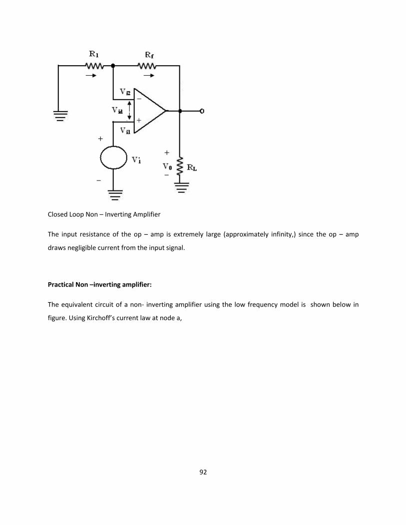
92
Closed Loop Non – Inverting Amplifier
The input resistance of the op – amp is extremely large (approximately infinity,) since the op – amp
draws negligible current from the input signal.
Practical Non –inverting amplifier:
The equivalent circuit of a non- inverting amplifier using the low frequency model is shown below in
figure. Using Kirchoff’s current law at node a,
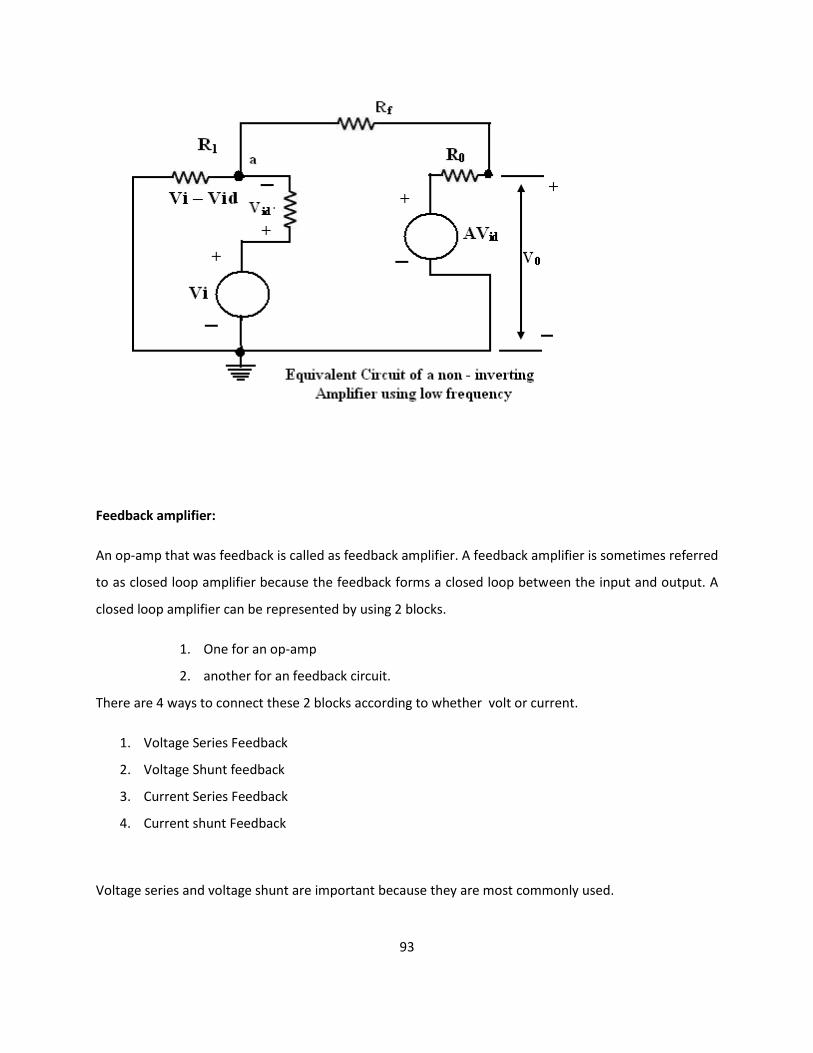
93
Feedback amplifier:
An op-amp that was feedback is called as feedback amplifier. A feedback amplifier is sometimes referred
to as closed loop amplifier because the feedback forms a closed loop between the input and output. A
closed loop amplifier can be represented by using 2 blocks.
1. One for an op-amp
2. another for an feedback circuit.
There are 4 ways to connect these 2 blocks according to whether volt or current.
1. Voltage Series Feedback
2. Voltage Shunt feedback
3. Current Series Feedback
4. Current shunt Feedback
Voltage series and voltage shunt are important because they are most commonly used.
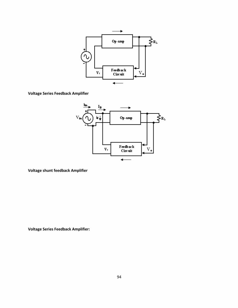
94
Voltage Series Feedback Amplifier
Voltage shunt feedback Amplifier
Voltage Series Feedback Amplifier:

95
Before Proceeding, it is necessary to define some terms.
Voltage gain of the op-amp with a without feedback:
Gain of the feedback circuit are defined as open loop volt gain (or gain without feedback) A = V0 / Vid
Closed loop volt gain (or gain with feedback) AF = V0 /Vin
Gain of the feedback circuit => B = VF /V0 .
1. Negative feedback:
KVL equation for the input loop is,
Vid = Vin -Vf -----(1)
Vin = input voltage.
Vf = feedback voltage.
Vid = difference input voltage.
The difference volt is equal to the input volt minus the f/b volt. (or) The feedback volt always opposes
the input volt (or out of phase by 1800 with respect to the input voltage) hence the feedback is said to be
negative.
It will be performed by computing

96
1. Closed loop volt gain
2. Input and output resistance
3. Bandwidth
1. Closed loop volt gain:
The closed loop volt gain is AF = V0 /Vin
V0 = Avid =A(V1 –V2 )
A = large signal voltage gain.
From the above eqn, V0 = A(V1 – V2 )
Refer fig, we see that, V1 = Vin
V2 = Vf = R1 V0
------
R1 +Rf Since Ri >> R1
V0 = AVin - R1 V0

97
------
R1 +Rf
V0 + A R1 V0 = AVin
------
R1 +Rf
Rearranging, we get,
In other words for given R1 and RF the values of AF and B are fixed. Finally, the closed loop voltage gain AF
can be expressed in terms of open loop gain A and feedback circuit gain B as follows,
3. Difference input voltage ideally zero (Vid)
Reconsider eqn V0 = A Vid
Vid = V0 /A
Since A is very large (ideally α )
Vid t 0 ---(7.a)
(i.e) V1 t V2 --(7.b)
says that the volt at the Non-inverting input terminal of an op-amp is approximately equal to that at the
inverting input terminal provided that A, is vey large.
From the circuit diagram,
V1 = Vin
V2 = VF = R1 V0 / R1 +RF

98
Sub these values of V1 and V2 in eqn (7.b) we get
Vin = R1 V0 / R1 +RF (i.e) AF = V0 /Vin = 1+RF /R1
4. Input Resistance with feedback:
From the below circuit diagram Ri -> input resistance
Rif -> input resistance of an op-amp with feedback
Derivation of input resistance with Feedback:
The input resistance with feedback is defined as,
5. Output Resistance with feedback:

99
This resistance can be obtained by using Thevenin’s theorem. To find out o/p resistance
with feedback ROF reduce independent source Vin to zero, apply an external voltage V0 , and calculate
the resulting current i0 .
The ROF is defined as follows,
ROF = V0 /i0 ---
KCL at o/p node ‘N’ we get,
i0 = ia + ib
Since ((RF + R1 )|| Ri >> R0 and i0 >> ib .
i0 t ia
The current i0 can be found by writing KVL eqn for the o/p loop
V0 – R0 i0 – AVid = 0
i0 = V0 – AVid

100
---------
R0
Vid = V1 - V2
= 0 - VF
This result shows that the output resistance of the voltage series feedback amplifier is 1/(1+AB) the
output resistance of R0 the op-amp. (i.e) The output resistance of the op-amp with feedback is much
smaller than the output resistance without feedback.
6. Bandwidth with feedback:
The bandwidth of the amplifier is defined as the band (range of frequency) for which the
gain remains constant. The Frequency at which the gain equals 1 is known as unity gain bandwidth
(UGB). The relationship between the breakfrequency f0 , open loop volt gain A, bandwidth with feedback
fF and closed loop gain AF .
For an op-amp with a single break frequency f0 , the gain bandwidth product is constant and equal to the
unity-gain bandwidth. (UGB).
UGB = (A) (f0 )
A = open loop volt gain
f0 = break frequency of an op-amp ((or) only for a single break frequency op-amp UGB = AF fF ----(10.b)
AF = closed loop volt gain
fF = bandwidth with feedback.
Af0 = AF fF
fF = Af0 /AF
For the non-inverting amplifier with feedback

101
AF = A/(1+AB)
Sub the value of AF in eqn 10.c, we get
fF = Af0 / A/(1+AB)
fF = (1+ AB) f0 eqn > bandwidth of the non-inverting amplifier with feedback is = bandwidth of the with
feedback f0 times (1+AB)
7. Total o/p offset voltage with feedback (Vout)
In an open loop op-amp the total o/p offset voltage is equal to either the +ve or –ve
saturation volt.
Vout = +ve (or) –ve saturation volt.
With feedback the gain of the Non-inverting amplifier changes from A to A/(1+AB), the total output
offset voltage with feedback must also be 1/(1+AB) times the voltage without feedback.
Total o/p offset Vout with feedback = Total o/p offset volt without feedback
---------------------------------------------
1+AB
Vout = ±Vsat
---------
1+AB
1/(1+AB) is < I and ±Vsat = Saturation voltages. The maximum voltages the output of an op-amp can
reach.
Note:

102
Open-loop even a very small volt at the input of an op-amps can cause to reach maximum value (+ Vsat
)because of its very high volt gain. According to eqn for a gain op-amp circuit the Vout is either +ve or –
ve volt because Vsat can be either +ve or –ve.
Conclusion of Non-Inverting Amplifier with feedback:
The char of the perfect volt Amplifier:
1. It has very high input resistamce.
2. Very low output resistance
3. Stable volt gain
4. large bandwidth
8. Voltage Follower: [Non-Inverting Buffer]
The lowest gain that can be obtained from a non-inverting amplifier feedback is 1. When
the Non-Inverting amplifier is designed for unity and it is called a voltage follower, because the output
voltage is equal to and inphase with the input or in volt follower the output follows the input.
It is similar to discrete emitter follower, the volt follower is preferred, because it had much higher input
resistance and output amplitude is exactly equal to input.
To obtain the voltage follower, from this circuit simply open R1 and short RF .
In this figure all the output volt is fed back into the inverting terminal of the op-amp.
The gain of the feedback circuit is 1 (B = AF =1)

103
AF = 1
RiF = ARi
ROF =R0 /A
fF = Af0
Vout = ±Vsat
---------
A
Since 1+ A t A.
Voltage Shunt Feedback Amplifier:[Inverting Amplifier]
The input voltage drives the inverting terminal, and amplified as well as inverted output signal also
applied to the inverting input via feedback resistor RF .
Note:
Non-inverting terminal is grounded and feedback circuit has RF and extra resistor R1 is connected in
series with the input signal source Vin.
We derive the formula for

104
1. Voltage gain
2. Input and output resistance
3. Bandwidth
4. Total output offset voltage.
1. Closed – loop voltage gain AF :
AF of volt shunt feedback amplifier can be obtained by writhing KCL eqn at the input node
V2 .
iin = iF + IB ----(12.a)
Since Ri is very large, the input bias current is negligibly small.
iin t iF
(i.e) Vin – V2 V2 – V0
------------ = --------------
Ri RF
Consider, from eqn,
V1 – V2 = - V0 /A
Since V1 = 0V
V2 = -V0 /A
Sub this value of V2 in eqn (12.b) and rearranging,
Vin +V0 /A -(V/A) - V0
-------------- = ----------------
Ri RF

105
AF = V0 ARF
---- = - -------- (exact)
Vin R1 +RF +AR1
The –ve sign indicates that the input and output signals are out of phase 1800 . (or opposite polarities).
Because of this phase inversion the diagram is known as Inverting amplifier with feedback. Since the
internal gain A of the op-amp is very large (α) , AR1 >> R1 + RF , (i.e) eqn (13)
AF = V0 /Vin = -RF /R1 (Ideal)
To express eqn (13) in terms of eqn(6). To begin with, we divide both numerator and denominator of
eqn (13) by (R1 + RF )
AF = ARF /R1 + RF
-----------------
1+ AR1 (R1 + RF )
AF = - AR/ 1+AB)
Where K = RF /(R1 + RF )
B = R1 /(R1 + RF ) Gain of feedback.

106
With feedback (6) indicates that in addition to the phase inversion (-sign), the closed loop gain of the
inverting amplifier in K times the closed loop gain of the Non-inverting amplifier where K< 1. To derive a
ideal closed loop gain,
If AB >> 1, then (1+AB) = AB and AF = K/B = -RF /R1
2. Input Resistance with feedback:
Easiest method of finding the input resistance is to millerize the feedback resistor RF .
(i.e) Split RF in to its 2 Miller components as shown in fig.
In this circuit, the input resistance with feedback Rif is then
Rif = R1 + RF
----- || (Ri)
1+A
Since Ri and A are very large.
R1 + RF
----- || (R1) t 0Ω

107
1+A
3. Output Resistance with feedback:
The output resistance with feedback ROF is the resistance measured at the output terminal
of the feedback amplifier. Thevenin’s circuit is exactly for the same as that of Non-inverting amplifier
because the output resistance ROF of the inverting amplifier must be identical to that of non – inverting
amplifier.
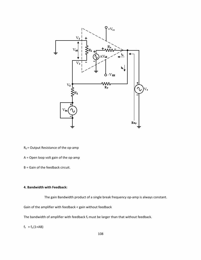
108
R0 = Output Resistance of the op-amp
A = Open loop volt gain of the op-amp
B = Gain of the feedback circuit.
4. Bandwidth with Feedback:
The gain Bandwidth product of a single break frequency op-amp is always constant.
Gain of the amplifier with feedback < gain without feedback
The bandwidth of amplifier with feedback fF must be larger than that without feedback.
fF = f0 (1+AB)

109
f0 = Break frequency of the op-amp
= unity gain Bandwidth UGB
---------------------------- = -------
Open- loop voltage gain A
fF = UGB
------- (1+AB)
A
fF = UGB (K)
-------
AF
Where K = RF /(R1 + RF ) ; AF = AK/1+AB
Eqn 10.b and 21.b => same for the bandwidth.
Same closed loop gain the closed loop bandwidth for the inverting amplifier is < that of Non – inverting
amplifier by a factor of K(<1)
5. Total output offset voltage with feedback:
When the temp & power supply are fixed, the output offset voltage is a function of the
gain of an op-amp.
Gain of the feedback < gain without feedback.
The output offset volt with feedback < without feedback.
Total Output offset Voltage with f/b =Total output offset volt without f/b

110
------------------------------------------
1+AB
Vout = ±Vsat
---------
1+AB
±Vsat = Saturation Voltage
A = open-loop volt gain of the op-amp
B = Gain of the f/b circuit
B= R1 /(R1 + RF )
In addition, because of the –ve f/b,
1. Effect of noise
2. Variations in supply voltages
3. Changes in temperature on the output voltage of inverting amplifier are reduced.
Differential amplifier:
We will evaluate 2 different arrangements of the differential amplifier with -ve feedback. Classify these
arrangements according to the number of op-amps used. i.e
1. Differential amplifier with one op-amp
2. Differential amplifier with two op-amps.

111
Differential amplifier are used in instrumentation and industrial applications to amplify differences
between 2 input signals such as output of the wheat stone bridge circuit.
Differential amplifier preferred to these application because they are better able to reject common
mode (noise) voltages than single input circuit such as inverting and non-inverting amplifier.
1. Differential Amplifier with one op-amp:
To analyse this circuit by deriving voltage gain and input resistance. This circuit is a
combination of inverting and non-inverting amplifier. (i.e) When Vx is reduced to zero the circuit is non-
inverting amplifier and when Vy is reduced to zero the circuit is inverting amplifier.
Voltage Gain:
The circuit has 2 inputs Vx and Vy . Use superposition theorem, when Vy = 0V, becomes inverting
amplifier. Hence the o/p due to Vx only is
Vox = -RF (Vx)
-------------

112
R1
Similarly, when Vx = 0V, becomes Non-inverting amplifier having a voltage divider network composed of
R2 and R3 at the Non – inverting input.
Note : the gain of the differential amplifier is same as that of inverting amplifier.
Input Resistance:
The input resistance Rif of the differential amplifier is resistance determined looking into
either one of the 2 input terminals with the other grounded,
With Vy = 0V,
Inverting amplifier, the input resistance which is,
RiFx ≈ R1
Similarly, ,Vx = 0V,
Non-inverting amplifier, the input resistance which is,
RiFy ≈ (R2 + R3 )
Vx and Vy are not the same. Both the input resistance can be made equal, if we modify the basic
differential amplifier. Both R1 and (R2 + R3) can be made much larger than the source resistances. So that
the loading of the signal sources does not occur.
Note: If we need a variable gain, we can use the differential amplifier. In this circuit R1 = R2 , RF = R3 and
the potentiometer Rp = R4.
Depending on the position of the wiper in R voltage can be varied from the closed loop gain of -2RF /R1
to the open loop gain of A.

113
2. Differential Amplifier with 2 op-amps:
We can increase the gain of the differential amplifier and also increase the input
resistance Rif if we use 2 op-amps.
Voltage gain:
It is compares of 2 stages 1. Non-inverting
2. Differential amplifier with gain.

114
By finding the gain of these 2 stages, we can obtain the overall gain of the circuit, The o/p
By applying superposition theorem to the second stage, we can obtain the output voltage,
Input Resistance:
The input resistance Rif of the differential amplifier is the resistance determined from either one of the
two non-inverting terminals with the other grounded. The first stage A1 is the non-inverting amplifier,
its input resistance is
RiFy = Ri (1+AB)
Where Ri = open loop input resistance of the op-amp.
B = R2 /R2 + R3
Similarly, with Vy shorted to ground (Vy = 0 V), the 2nd stage (A2 ) also becomes non-inverting amplifier,
whose input resistance is
RiFx = Ri (1+AB)
Where Ri = open loop input resistance of the op-amp
B = R1 /(R1 + RF)
Since R1 = R3 and RF = R2 , the Rify ≠ RiFx because the loading of the input sources Vx and Vy may occur.
(Or)
The output signal may be smaller in amplitude than expected. This possible reduction in the amplitude
of the output signal is drawback of differential amplifier.
To overcome this:
With proper selection of components, both RiFy and RiFx can be made much larger than the sources
resistance so that the loading of the input sources does not occur.
Output resistance and Bandwidth of differential amplifier with feedback:

115
The output resistance of the differential amplifier should be the same as that of the non-
inverting amplifier expect that B = 1/AD (i.e)
ROF = R0 /(1+A/AD )
AD = closed loop gain of the differential amplifier
R0 = output resistance of the op-amp
A = open – loop volt gain of the op-amp
Remember that AD is different for differential amplifier.
In the case of Inverting and Non-inverting amplifier, the bandwidth of the differential amplifier also
depends on the closed loop gain of the amplifier and is given by,
fF = Unity gain Bandwidth
-----------------------------
closed loop gain AD
SIGN CHANGER (PHASE INVERTER)

116
The basic inverting amplifier configuration using an op-amp with input impedance Z 1 and
feedback impedance Z f .
If the impedance Z 1 and Z f are equal in magnitude and phase, then the closed loop voltage gain
is -1,and the input signal will undergo a 1800 phase shift at the output. Hence, such circuit is also called
phase inverter. If two such amplifiers are connected in cascade, then the output from the second stage
is the same as the input signal without any change of sign.
Hence, the outputs from the two stages are equal in magnitude but opposite in phase and
such a system is an excellent paraphase amplifier.
Scale Changer:
Referring the above diagram, if the ratio Zf / Z1 = k, a real constant, then the closed loop gain is –
k, and the input voltage is multiplied by a factor –k and the scaled output is available at the output.
Usually, in such applications, Zf and Z1 are selected as precision resistors for obtaining precise and scaled
value of input voltage.
PHASE SHIFT CIRCUITS
The phase shift circuits produce phase shifts that depend on the frequency and maintain a
constant gain. These circuits are also called constant-delay filters or all-pass filters. That constant delay
refers to the fact the time difference between input and output remains constant when frequency is
changed over a range of operating frequencies.
This is called all-pass because normally a constant gain is maintained for all the frequencies
within the operating range. The two types of circuits, for lagging phase angles and leading phase angles.
Phase-lag circuit:
Phase log circuit is constructed using an op-amp, connected in both inverting and non inverting
modes. To analyze the circuit operation, it is assumed that the input voltage v1 drives a simple inverting
amplifier with inverting input applied at(-)terminal of op-amp and a non inverting amplifier with a low-
pass filter.

117
It is also assumed that inverting gain is -1 and non-inverting gain after the low-pass circuit is
1R f
R1
ffffffff =1+1=2, Since R f =R1
For the circuit fig a ,it can be written as
V o j Ab c
@Vi jb c 2
1
1 j Rcfffffffffffffffffffffffffff
f g
Vi jb c
Therefore,

118
V o j Ab c
V i jb cd e
@1 21
1 j Rcfffffffffffffffffffffffffff
f g
Vi jb c
h
j
i
k Vi jwb c
1 @jwRC
1 jwRCffffffffffffffffffffffffffffff
The relationship between output and input can be expressed by
V 0 jwb c
V 1 jwb c
fffffffffffffffffffffffff 1 @jwRC
1 jwRCffffffffffffffffffffffffffffffF G
The relationship is complex as defined above equation and it shows that it has both magnitude
and phase. Since the numerator and denominator are complex conjugates, their magnitudes are
identical and the overall phase angle equals the angle of numerator less the angle of the denominator.
The phase angle is than given by
@tan@1
wRC` a
@tan@1
wRC` a
@2 tan@1
wRC` a
@@@@3` a
Hence, when w=0, the phase angle approaches zero. When w=∞, the phase angle approaches -1800 .
The Equation (3) becomes as
@2tan@1 f
f0
ffffffff
h
j
i
k @@@@@ 4` a
Where the frequency f0 is given by
f0
1
2 RCfffffffffffffffffff
@@@5` a
Here, when f=f0 in eq.4, the phase angle θ = -900 . The Bode plot for
the phase-lag circuit is shown in fig.b
Phases-lead circuit:

119
It is to noted that the numerator has a negative real part and overall phase is given by
1800@tan@1
wRC` a
@tan@1
wRC` a
1800@2 tan@1
wRC` a
@@@@3` a
When the frequency approaches zero,the phase angle approaches 180o As the frequency is increased,
the leading phase decrease and it finally approaches zero at high frequencies. Hence can be written as
180o@2tan@1
f
fo
ffffffff
h
j
i
k
Where fo= 1
2 RCffffffffffffffffffff
Bode plot for the phase-lead circuit of below fig

120
Voltage follower:
If R1=∞ and Rf=0 in the non inverting amplifier configuration .
The amplifier act as a unity-gain amplifier or voltage follower.
That is
Av 1R f
R1
ffffffffor
R f
R1
ffffffffAv @1
Since R f
R1
ffffffff0 Av 1
The circuit consist of an op-amp and a wire connecting the output voltage to the input ,i.e the
output voltage is equal to the input voltage, both in magnitude and phase.V0=Vi
Since the output voltage of the circuit follows the input voltage, the circuit is called voltage
follower. It offers very high input impedance of the order of MΩ and very low output impedance.
Therefore, this circuit draws negligible current from the source. Thus, the voltage follower can
be used as a buffer between a high impedance source and a low impedance load for impedance
matching applications.

121
Voltage to Current Converter with floating loads (V/I):
1. Voltage to current converter in which load resistor RL is floating (not connected to ground).
2. Vin is applied to the non inverting input terminal, and the feedback voltage across R1 devices the
inverting input terminal.
3. This circuit is also called as a current – series negative feedback amplifier.
4. Because the feedback voltage across R1 (applied Non-inverting terminal) depends on the output
current i0 and is in series with the input difference voltage Vid .

122
Writing KVL for the input loop,
Vin V id V f
V idt 0v , since A is very largeA
Vin V f
Vin R1 i0 or` a
i0
Vin
R1
ffffffff
From the fig input voltage Vin is converted into output current of Vin/R1 [Vin -> i0 ] . In
other words, input volt appears across R1. If R1 is a precision resistor, the output current (i0 = Vin/R1 )
will be precisely fixed.
Applications:
1. Low voltage ac and dc voltmeters
2. Diode match finders
3. LED
4. Zener diode testers.
Voltage – to current converter with Grounded load:
This is the other type V – I converter, in which one terminal of the load is connected to
ground.

123
Analysis of the circuit:
The analysis of the circuit can be done by following 2 steps.
1. To determine the voltage V1 at the non-inverting (+) terminals and
2. To establish relationship between V1 and the load current IL .
Applying KCL at node V1 we can write that,
Current to Voltage Converter (I –V):
1. Open – loop gain a of the op-amp is very large.
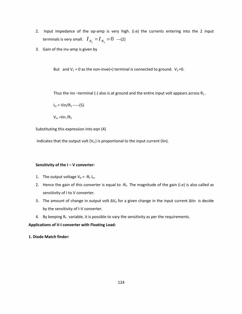
124
2. Input impedance of the op-amp is very high. (i.e) the currents entering into the 2 input
terminals is very small. I B1
I B2
0 ---(2)
3. Gain of the inv-amp is given by
But and V1 = 0 as the non-inve(+) terminal is connected to ground. V2 =0.
Thus the inv –terminal (-) also is at ground and the entire input volt appears across R1 .
Iin = Vin/R1 -----(5)
Vin =Iin /R1
Substituting this expression into eqn (4)
indicates that the output volt (V0 ) is proportional to the input current (Iin).
Sensitivity of the I – V converter:
1. The output voltage V0 = -RF Iin.
2. Hence the gain of this converter is equal to -RF. The magnitude of the gain (i.e) is also called as
sensitivity of I to V converter.
3. The amount of change in output volt ∆V0 for a given change in the input current ∆Iin is decide
by the sensitivity of I-V converter.
4. By keeping RF variable, it is possible to vary the sensitivity as per the requirements.
Applications of V-I converter with Floating Load:
1. Diode Match finder:

125
In some applications, it is necessary to have matched diodes with equal voltage drops at a
particular value of diode current. The circuit can be used in finding matched diodes and is obtained from
fig (V-I converter with floating load) by replacing RL with a diode. When the switch is in position 1: (Diode
Match Finder) Rectifierr diode (IN 4001) is placed in the f/b loop, the current through this loop is set by
input voltage Vin and Resistor R1 . For Vin = 1V and R1 = 100Ω, the current through this
I0 = Vin/R1 = 1/100 = 10mA.
As long as V0 and R1 constant, I0 will be constant. The Voltage drop across the diode can be found either
by measuring the volt across it or o/p voltage. The output voltage is equal to (Vin + VD ) V0 = Vin + VD . To
avoid an error in output voltage the op-amp should be initially nulled. Thus the matched diodes can be
found by connecting diodes one after another in the feedback path and measuring voltage across them.
2. Zener diode Tester:
(When the switch position 2)
when the switch is in position 2, the circuit becomes a zener diode tester. The circuit can be used to find
the breakdown voltage of zener diodes. The zener current is set at a constant value by Vin and R1. If this
current is larger than the knee current (IZK ) of the zener, the zenerr blocks (Vz ) volts.

126
For Ex:
IZK = 1mA , VZ = 6.2V, Vin = 1v , R1 = 100Ω Since the current through the zener is , I0 = Vin/R1 = 1/100
=10mA > IZK the voltage across the zener will be approximately equal to 6.2V.
3. When the switch is in position 3: (LED)
The circuit becomes a LED when the switch is in position 3. LED current is set at a constant
value by Vin and R1. LEDs can be tested for brightness one after another at this current. Matched LEDs
with equal brightness at a specific value of current are useful as indicates and display devices in digital
applications.
Applications of I – V Converter:
One of the most common use of the current to voltage converter is
1. Digital to analog Converter (DAC)
2. Sensing current through Photodetector. Such as photocell, photodiodes and photovoltaic cells.
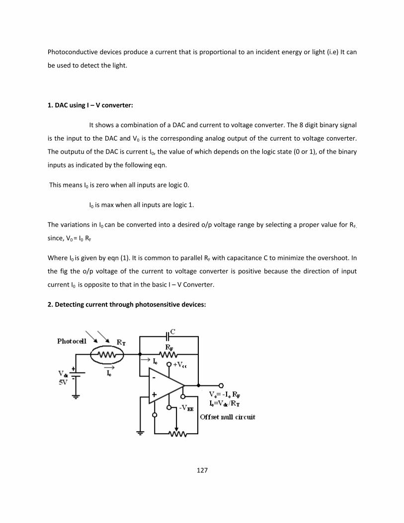
127
Photoconductive devices produce a current that is proportional to an incident energy or light (i.e) It can
be used to detect the light.
1. DAC using I – V converter:
It shows a combination of a DAC and current to voltage converter. The 8 digit binary signal
is the input to the DAC and V0 is the corresponding analog output of the current to voltage converter.
The outputu of the DAC is current I0, the value of which depends on the logic state (0 or 1), of the binary
inputs as indicated by the following eqn.
This means I0 is zero when all inputs are logic 0.
I0 is max when all inputs are logic 1.
The variations in I0 can be converted into a desired o/p voltage range by selecting a proper value for RF.
since, V0 = I0 RF
Where I0 is given by eqn (1). It is common to parallel RF with capacitance C to minimize the overshoot. In
the fig the o/p voltage of the current to voltage converter is positive because the direction of input
current I0 is opposite to that in the basic I – V Converter.
2. Detecting current through photosensitive devices:

128
Photocells, photodiodes, photovoltaic cells give an output curren that depends on the
intensity of light and independent of the load. The current through this devices can be converted to
voltage by I – V converter and it can be used as a measure of the amount of light. In this fig photocell is
connected to the I – V Converter. Photocell is a passive transducer, it requires an external dc
voltage(Vdc). The dc voltage can be eliminated if a photovoltaic cell is used instead of a photocell. The
Photovoltaic Cell is a semiconductor device that converts the radiant energy to electrical power. It is a
self generating circuit because it doesnot require dc voltage externally. Ex of Photovoltaic Cell : used in
space applications and watches.
Summing Amplifier:
Op-amp may be used to design a circuit whose output is the sum of several input signals. Such a
circuit is called a summing amplifier or a summer.
An inverting summer or a non-inverting summer may be discussed now.
Inverting Summing Amplifier:
A typical summing amplifier with three input voltages V1, V2 and V3 three input resistors R1, R2,
R3 and a feedback resistor Rf is shown in figure 2.

129
The following analysis is carried out assuming that the op-amp is an ideal one, that is, AOL = ∞.
Since the input bias current is assumed to be zero, there is no voltage drop across the resistor Rcomp and
hence the non-inverting input terminal is at ground potential.
Thus the output in an inverted, weighted sum of the inputs. In the special case, when R1 = R2 =
R3 = Rf, we have
V o @ V 1 V 2 V 3
b c
in such case the output Vo is the inverted sum of the input signals. We may also set
R1 R2 R3 3Rf
in which case
Thus the output is the average of the input signals (inverted). In a practical circuit, input bias
current compensating resistor Rcomp should be provided.
To find Rcomp, make all inputs V1 = V2 = V3 = 0. So the effective input resistance Ri = R1 || R2 || R3.
Therefore, Rcomp = Ri || Rf = R1 || R2 || R3 || R,f.
Non-Inverting Summing Amplifier:
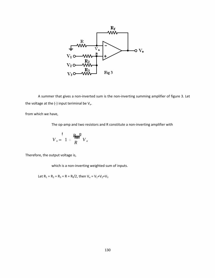
130
A summer that gives a non-inverted sum is the non-inverting summing amplifier of figure 3. Let
the voltage at the (-) input teriminal be Va.
from which we have,
The op-amp and two resistors and R constitute a non-inverting amplifier with
V o 1
Rf
R
fffffffff g
V a
Therefore, the output voltage is,
which is a non-inverting weighted sum of inputs.
Let R1 = R2 = R3 = R = Rf/2, then Vo = V1+V2+V3

131
Subtractor:
A basic differential amplifier can be used as a subtractor as shown in the above figure. If all
resistors are equal in value, then the output voltage can be derived by using superposition principle.
To find the output V01 due to V1 alone, make V2 = 0.
Then the circuit of figure as shown in the above becomes a non-inverting amplifier having input
voltage V1/2 at the non-inverting input terminal and the output becomes
V 01
V 1
2
ffffffff1
R
R
ffffff g
V 1
Similarly the output V02 due to V2 alone (with V1 grounded) can be written simply for an
inverting amplifier as
V 02 @V 2
Thus the output voltage Vo due to both the inputs can be written as
V o V 01 V 02 V 1 @V 2

132
Adder/Subtractor:
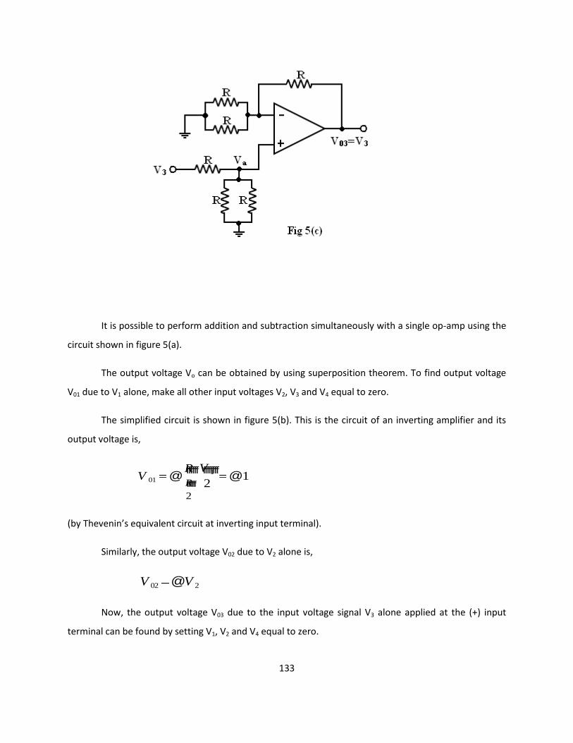
133
It is possible to perform addition and subtraction simultaneously with a single op-amp using the
circuit shown in figure 5(a).
The output voltage Vo can be obtained by using superposition theorem. To find output voltage
V01 due to V1 alone, make all other input voltages V2, V3 and V4 equal to zero.
The simplified circuit is shown in figure 5(b). This is the circuit of an inverting amplifier and its
output voltage is,
V 01 @
R
R
2
fffffff
ffffffV 1
2
ffffffff@1
(by Thevenin’s equivalent circuit at inverting input terminal).
Similarly, the output voltage V02 due to V2 alone is,
V 02 @V 2
Now, the output voltage V03 due to the input voltage signal V3 alone applied at the (+) input
terminal can be found by setting V1, V2 and V4 equal to zero.

134
The circuit now becomes a non-inverting amplifier as shown in figure 5(c). The voltage Va at the
non-inverting terminal is
V a
R
2
fffffff
RR
2
fffffff
ffffffffffffffffffV 3
V 3
3
ffffffff
So, the output voltage V03 due to V3 alone is
V 03 1
R
R
2
fffffff
ffffff
h
lj
i
mk V a 3
V 3
3
fffffffff g
V 3
Similarly, it can be shown that the output voltage V04 due to V4 alone is
V 04 V 4
Thus, the output voltage Vo due to all four input voltages is given by
V o V 01 V 02 V 03 V 04
V o @V 1 @V 2 V 3 V 4
V o V 3 V 4
b c@ V 1 V 2
b c
So, the circuit is an adder-subtractor.
Instrumentation Amplifier:

135

136
In a number of industrial and consumer applications, one is required to measure and control
physical quantities.
Some typical examples are measurement and control of temperature, humidity, light intensity,
water flow etc. these physical quantities are usually measured with help of transducers.
The output of transducer has to be amplified so that it can drive the indicator or display system. This
function is performed by an instrumentation amplifier. The important features of an instrumentation
amplifier are
1. high gain accuracy
2. high CMRR
3. high gain stability with low temperature coefficient
4. low output impedance
There are specially designed op-amps such as µA725 to meet the above stated requirements of a
good instrumentation amplifier. Monolithic (single chip) instrumentation amplifier are also available
commercially such as AD521, AD524, AD620, AD624 by Analog Devices, LM363.XX (XX -->10,100,500) by
National Semiconductor and INA101, 104, 3626, 3629 by Burr Brown.
Consider the basic differential amplifier as shown in figure 6(a). It can be easily seen that the
output voltage Vo is given by,

137
Or,
For R1/R2 = R3/R4, we obtain
V o
R2
R1
fffffffV 1 @V 2
b c
In the circuit of figure 6(a), source V1 sees an input impedance = R3+R4 (=101K) and the
impedance seen by source V2 is only R1 (1K). This low impedance may load the signal source heavily.
Therefore, high resistance buffer is used preceding each input to avoid this loading effect as
shown in figure 6(b).
The op-amp A1 and A2 have differential input voltage as zero. For V1=V2, that is, under common
mode condition, the voltage across R will be zero. As no current flows through R and R’ the non-
inverting amplifier.
A1 acts as voltage follower, so its output V2’=V2. Similarly op-amp A2 acts as voltage follower
having output V1’=V1. However, if V1≠V2, current flows in R and R’, and (V2’-V1’)>(V2-V1). Therefore, this
circuit has differential gain and CMRR more compared to the single op-amp circuit of figure 6(a).
The output voltage Vo can be calculated as follows
The voltage at the (+) input terminal of op-amp A3 is . Using superposition theorem, we have,
Since, no current flows into op-amp, the current I flowing (upwards) in R is I=(V1-V2)/R and
passes through the resistor R’.
and
Putting the values of V1’ and V2’ in equation (1), we obtain,
Or,
In equation (2), if we choose R2 = R1 = 25K (say) and R’ = 25K; R = 50Ω, then a gain of can be
achieved.

138
The difference gain of this instrumentation amplifier R, however should never be made zero, as
this will make the gain infinity. To avoid such a situation, in a practical circuit, a fixed resistance in series
with a potentiometer is used in place of R.
Figure 6(c) shows a differential instrumentation amplifier using Transducer Bridge. The circuit
uses a resistive transducer whose resistance changes as a function of the physical quantity to be
measured.
The bridge is initially balanced by a dc supply voltage Vdc so that V1=V2. As the physical quantity
changes, the resistance RT of the transducer also changes, causing an unbalance in the bridge (V1≠V2).
This differential voltage now gets amplified by the three op-amp differential instrumentation amplifier.
There are number differential applications of instrumentation amplifier with the transducer
bridge, such as temperature indicator, temperature controller, and light intensity meter to name a few.
Differentiator:
One of the simplest of the op-amp circuits that contains capacitor in the differentiating
amplifier.
Differentiator:
As the name implies, the circuit performs the mathematical operation of differentiation
(i.e) the output waveform is the derivative of the input waveform. The differentiator may be
constructed from a basic inverting amplifier if an input resistor R1 is replaced by a capacitor C1 .
The expression for the output voltage can be obtained KCL eqn written at node V2 as follows,
Since the differentiator performs the reverse of the integrator function.
Thus the output V0 is equal to RF C1 times the negative rate of change of the input voltage Vin with time.
The –sign => indicates a 1800 phase shift of the output waveform V0 with respect to the input signal.
The below circuit will not do this because it has some practical problems.
The gain of the circuit (RF /XC1 ) R with R in frequency at a rate of 20dB/decade. This makes the circuit
unstable.

139
Also input impedance XC1 S with R in frequency which makes the circuit very susceptible to high
frequency noise.
Basic Differetntiator
From the above fig, fa = frequency at which the gain is 0dB and is given by,
Both stability and high frequency noise problems can be corrected by the addition of 2 components. R1
and CF . This circuit is a practical differentiator.
From Frequency f to feedback the gain Rs at 20dB/decade after feedback the gain S at 20dB/decade.
This 40dB/ decade change in gain is caused by the R1 C1 and RF CF combinations.
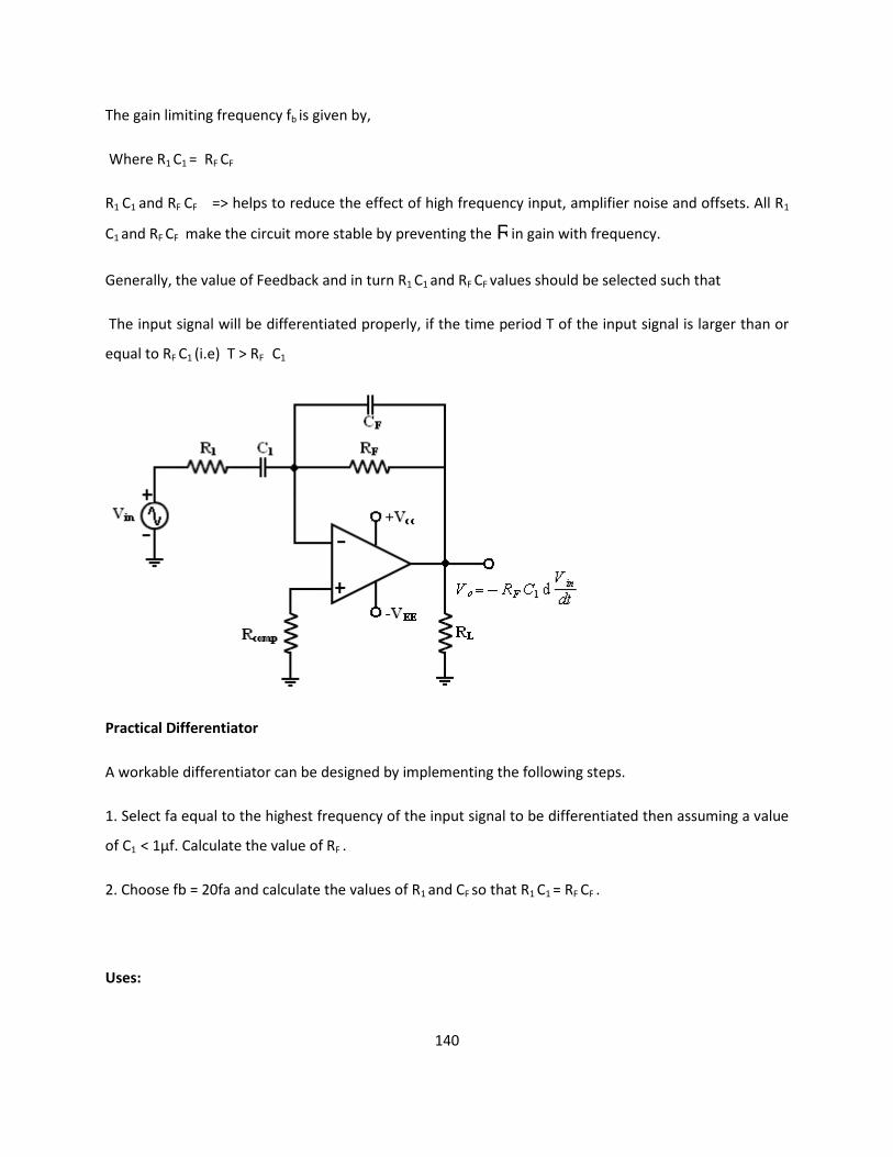
140
The gain limiting frequency fb is given by,
Where R1 C1 = RF CF
R1 C1 and RF CF => helps to reduce the effect of high frequency input, amplifier noise and offsets. All R1
C1 and RF CF make the circuit more stable by preventing the R in gain with frequency.
Generally, the value of Feedback and in turn R1 C1 and RF CF values should be selected such that
The input signal will be differentiated properly, if the time period T of the input signal is larger than or
equal to RF C1 (i.e) T > RF C1
Practical Differentiator
A workable differentiator can be designed by implementing the following steps.
1. Select fa equal to the highest frequency of the input signal to be differentiated then assuming a value
of C1 < 1μf. Calculate the value of RF .
2. Choose fb = 20fa and calculate the values of R1 and CF so that R1 C1 = RF CF .
Uses:

141
Its used in waveshaping circuits to detect high frequency components in an input signal and also as a
rate of change and detector in FM modulators.
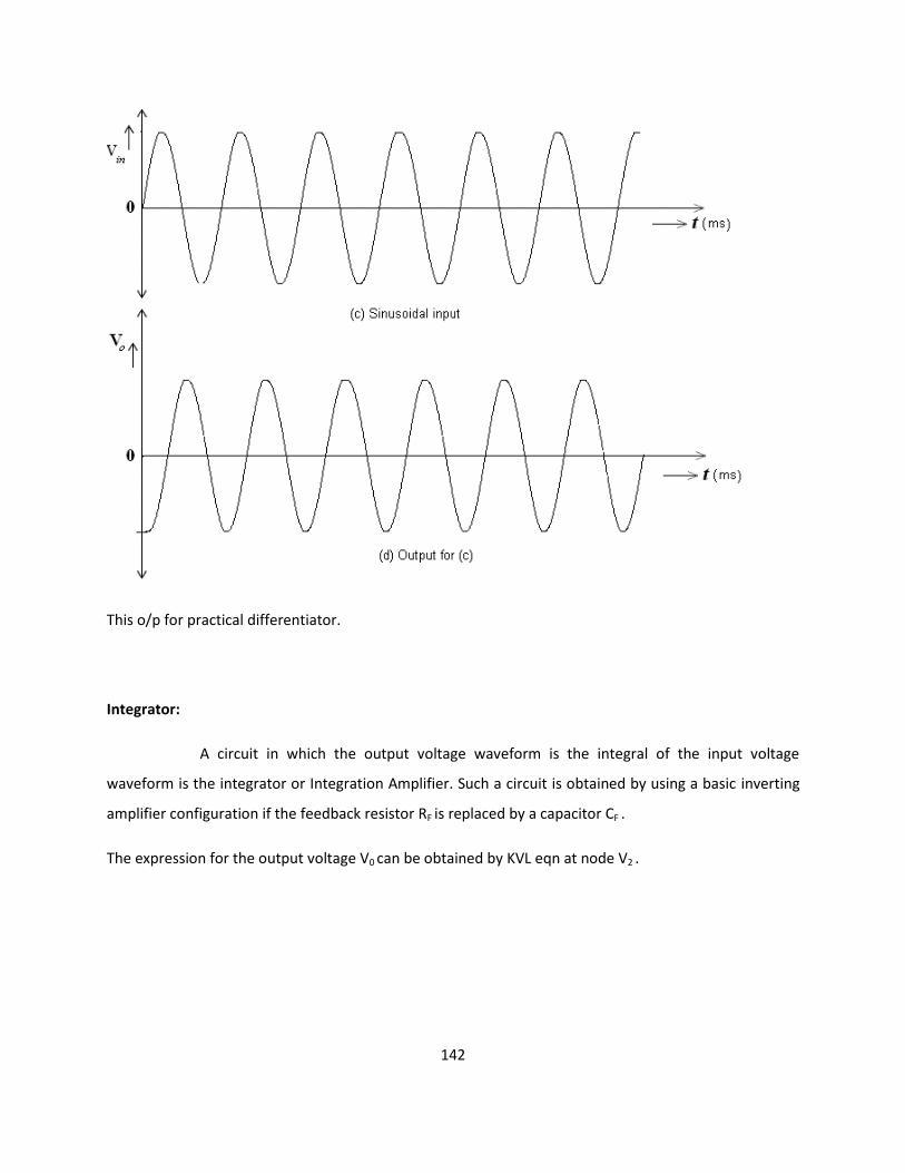
142
This o/p for practical differentiator.
Integrator:
A circuit in which the output voltage waveform is the integral of the input voltage
waveform is the integrator or Integration Amplifier. Such a circuit is obtained by using a basic inverting
amplifier configuration if the feedback resistor RF is replaced by a capacitor CF .
The expression for the output voltage V0 can be obtained by KVL eqn at node V2 .

143
eqn (3) indicates that the output is directly proportional to the negative integral of the input volts and
inversely proportional to the time constant R1 CF .
Ex: If the input is sine wave -> output is cosine wave.
If the input is square wave -> output is triangular wave.
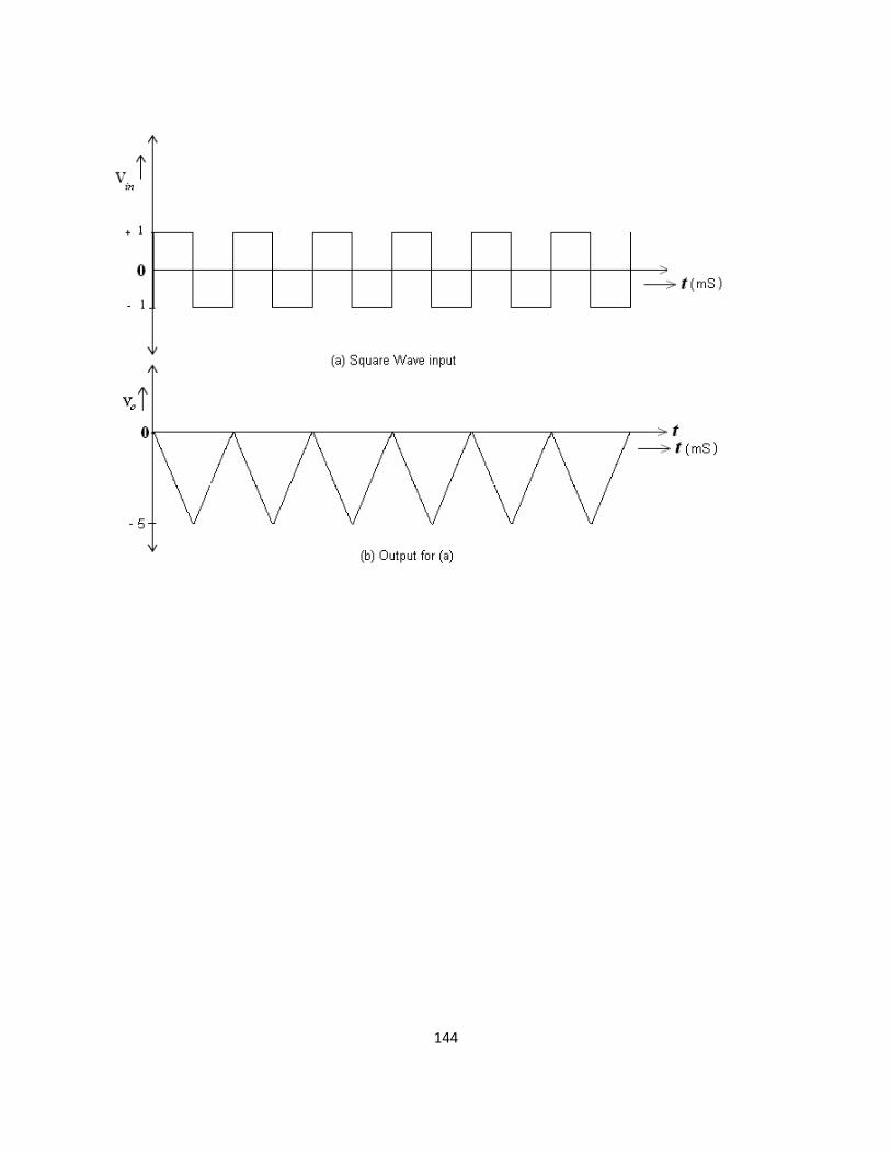
144
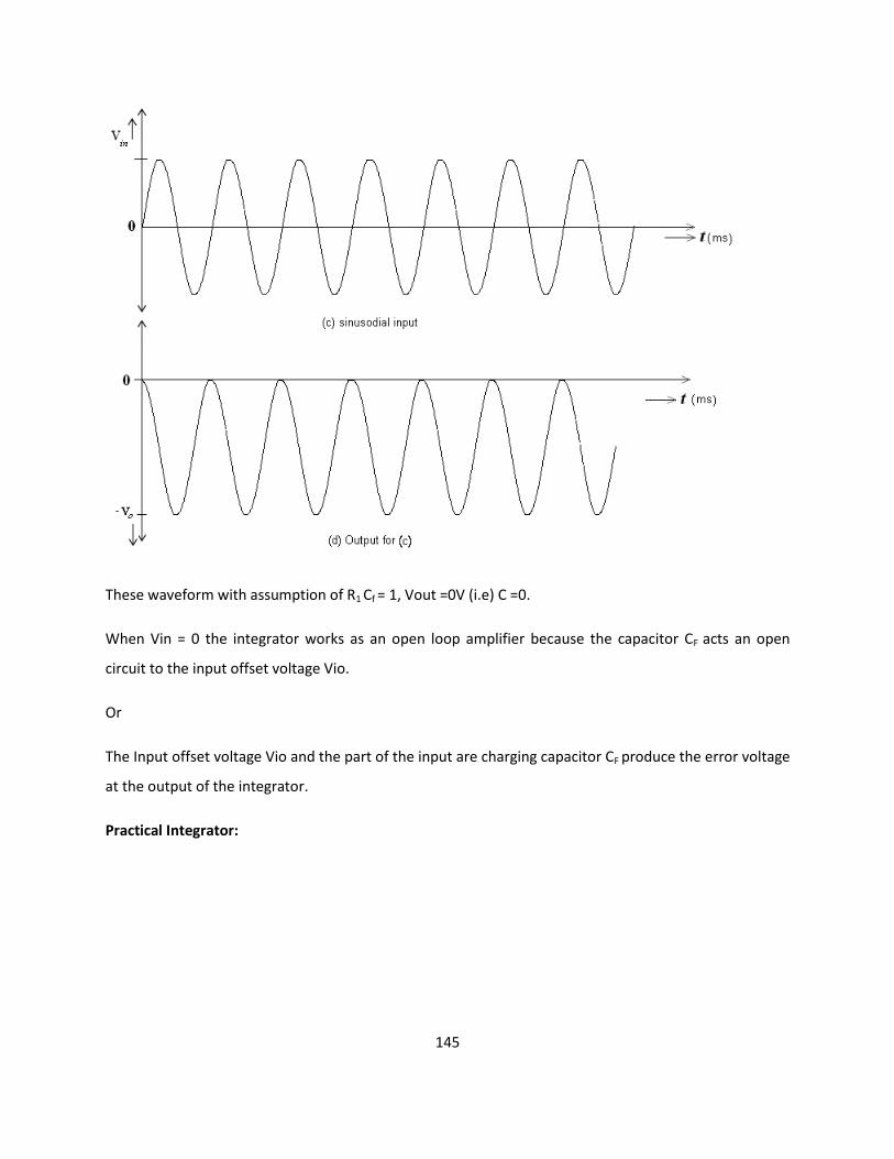
145
These waveform with assumption of R1 Cf = 1, Vout =0V (i.e) C =0.
When Vin = 0 the integrator works as an open loop amplifier because the capacitor CF acts an open
circuit to the input offset voltage Vio.
Or
The Input offset voltage Vio and the part of the input are charging capacitor CF produce the error voltage
at the output of the integrator.
Practical Integrator:

146
Practical Integrator to reduce the error voltage at the output, a resistor RF is connected across the
feedback capacitor CF .
Thus RF limits the low frequency gain and hence minimizes the variations in the output voltages.
Both the stability and low frequency roll-off problems can be corrected by the addition of a resistor RF in
the practical integrator.
Stability -> refers to a constant gain as frequency of an input signal is varied over a certain range.
Low frequency -> refers to the rate of decrease in gain roll off at lower frequencies.
From the fig of practical Integrators,
f is some relative operating frequency and for frequencies f to fa to gain RF / R1 is constant. After fa the
gain decreases at a rate of 20dB/decade or between fa and fb the circuit act as an integrator.
Generally the value of fa and in turn R1 CF and RF CF values should be selected such that fa<fb. In fact, the
input signal will be integrated properly if the time period T of the signal is larger than or equal to RF CF,
(i.e)
Uses:
Most commonly used in analog computers.

147
ADC
Signal wave shaping circuits.
Antilog Amplifier
The Circuit is shown in fig .The input Vi for the antilog-amp is fed into the temperature
compensating voltage divider R2 and RTC and then to the base of Q2 . The output Vo of the antilog-amp is
fed back to the inverting input of A1 through the resistor R1.
And
Since the base of Q1 is tied to ground, we get
The base voltage VB of Q2 is
The voltage at the emitter of Q2 is
V Q2B @E V B V Q2 E @B
Or
But the emitter voltage of Q2 is VA, that is
VA =VQ2B-E

148
Comparator
To obtain for better performance, we shall also look at integrated designed specifically as comparators
and converters. A comparator as its name implies, compares a signal voltage on one input of an op-amp
with a known voltage called a reference voltage on the other input. Comparators are used in circuits
such as,
Digital Interfacing
Schmitt Trigger
Discriminator
Voltage level detector and oscillators
1. Non-inverting Comparator:
A fixed reference voltage Vref of 1 V is applied to the negative terminal and time varying
signal voltage Vin is applied tot the positive terminal.When Vin is less than Vref the output becomes V0

149
at –Vsat [Vin < Vref => V0 (-Vsat)]. When Vin is greater than Vref, the (+) input becomes positive, the V0
goes to +Vsat. [Vin > Vref => V0 (+Vsat)]. Thus the V0 changes from one saturation level to another. The
diodes D1 and D2 protects the op-amp from damage due to the excessive input voltage Vin. Because of
these diodes, the difference input voltage Vid of the op-amp diodes are called clamp diodes. The
resistance R in series with Vin is used to limit the current through D1 and D2 . To reduce offset problems,
a resistance Rcomp = R is connected between the (-ve) input and Vref.
Input and Output Waveforms:
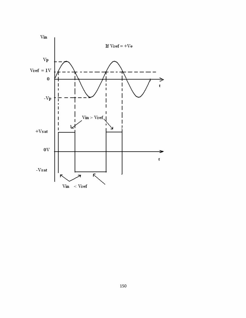
150

151
2. Inverting Comparator:

152
This fig shows an inverting comparator in which the reference voltage Vref is applied to the (+) input
terminal and Vin is applied to the (-) input terminal. In this circuit Vref is obtained by using a 10K
potentiometer that forms a voltage divider with dc supply volt +Vcc and -1 and the wiper connected to
the input. As the wiper is moved towards +Vcc, Vref becomes more positive. Thus a Vref of a desired
amplitude and polarity can be obtained by simply adjusting the 10k potentiometer.

153
3. Zero Crossing Detector: [ Sine wave to Square wave converter]

154
One of the application of comparator is the zero crossing detector or “sine wave to Square
wave Converter”. The basic comparator can be used as a zero crossing detector by setting Vref is set to
Zero. (Vref =0V).
This Fig shows when in what direction an input signal Vin crosses zero volts. (i.e) the o/p V0 is driven into
negative saturation when the input the signal Vin passes through zero in positive direction. Similarly,
when Vin passes through Zero in negative direction the output V0 switches and saturates positively.
Drawbacks of Zero- crossing detector:
In some applications, the input Vin may be a slowly changing waveform, (i.e) a low frequency signal. It
will take Vin more time to cross 0V, therefore V0 may not switch quickly from one saturation voltage to
the other. Because of the noise at the op-amp’s input terminals the output V0 may fluctuate between 2
saturations voltages +Vsat and –Vsat. Both of these problems can be cured with the use of regenerative
or positive feedback that cause the output V0 to change faster and eliminate any false output transitions

155
due to noise signals at the input. Inverting comparator with positive feedback . This is known as “Schmitt
Trigger”.
Schmitt Trigger: [Square Circuit]

156
This circuit converts an irregular shaped waveform to a square wave or pulse. The circuit is
known as Schmitt Trigger or squaring circuit. The input voltage Vin triggers (changes the state of) the
o/p V0 every time it exceeds certain voltage levels called the upper threshold Vut and lower threshold
voltage. These threshold voltages are obtained by using theh voltage divider R1 – R2, where the voltage
across R1 is feedback to the (+) input. The voltage across R1 is variable reference threshold voltage that
depends on the value of the output voltage. When V0 = +Vsat, the voltage across R1 is called “upper
threshold” voltage Vut. The input voltage Vin must be more positive than Vut in order to cause the
output V0 to switch from +Vsat to –Vsat. As long as Vin < Vut , V0 is at +Vsat, using voltage divider rule,
V ut
R1
R1 R2
ffffffffffffffffffV sat
b c
A

157
Similarly, when V0 = -Vsat, the voltage across R1 is called lower threshold voltage Vlt . the vin must be
more negative than Vlt in order to cause V0 to switch from –Vsat to +Vsat. In other words, for Vin > Vlt ,
V0 is at –Vsat. Vlt is given by the following eqn. V lt
R1
R1 R2
ffffffffffffffffff@V sat
b c
A
Thus, if the threshold voltages Vut and Vlt are made larger than the input noise voltages, the positive
feedback will eliminate the false o/p transitions. Also the positive feedback, because of its regenerative
action, will make V0 switch faster between +Vsat and –Vsat. Resistance Rcomp t R1 || R2 is used to
minimize the offset problems. The comparator with positive feedback is said to exhibit hysteresis, a
dead band condition. (i.e) when the input of the comparator exceeds Vut its output switches from +Vsat
to –Vsat and reverts to its original state, +Vsat when the input goes below Vlt. The hysteresis voltage is
equal to the difference between Vut and Vlt. Therefore
Vref = Vut – Vlt
Vref = R1
---------
R1 + R2 [+Vsat -(-Vsat)]
Precision Rectifier:
The signal processing applications with very low voltage, current and power levels require
rectifier circuits. The ordinary diodes cannot rectify voltages below the cut-in-voltage of the diode. A
circuit which can act as an ideal diode or precision signal – processing rectifier circuit for rectifying
voltages which are below the level of cut-in voltage of the diode can be designed by placing the diode in
the feedback loop of an op-amp.
Precision diodes:
Figure shows the arrangement of a precision diode. It is a single diode arrangement and functions as a
non-inverting precision half – wave rectifier circuit. If V1 in the circuit of figure is positive, the op-amp
output VOA also becomes positive. Then the closed loop condition is achieved for the op-amp and the
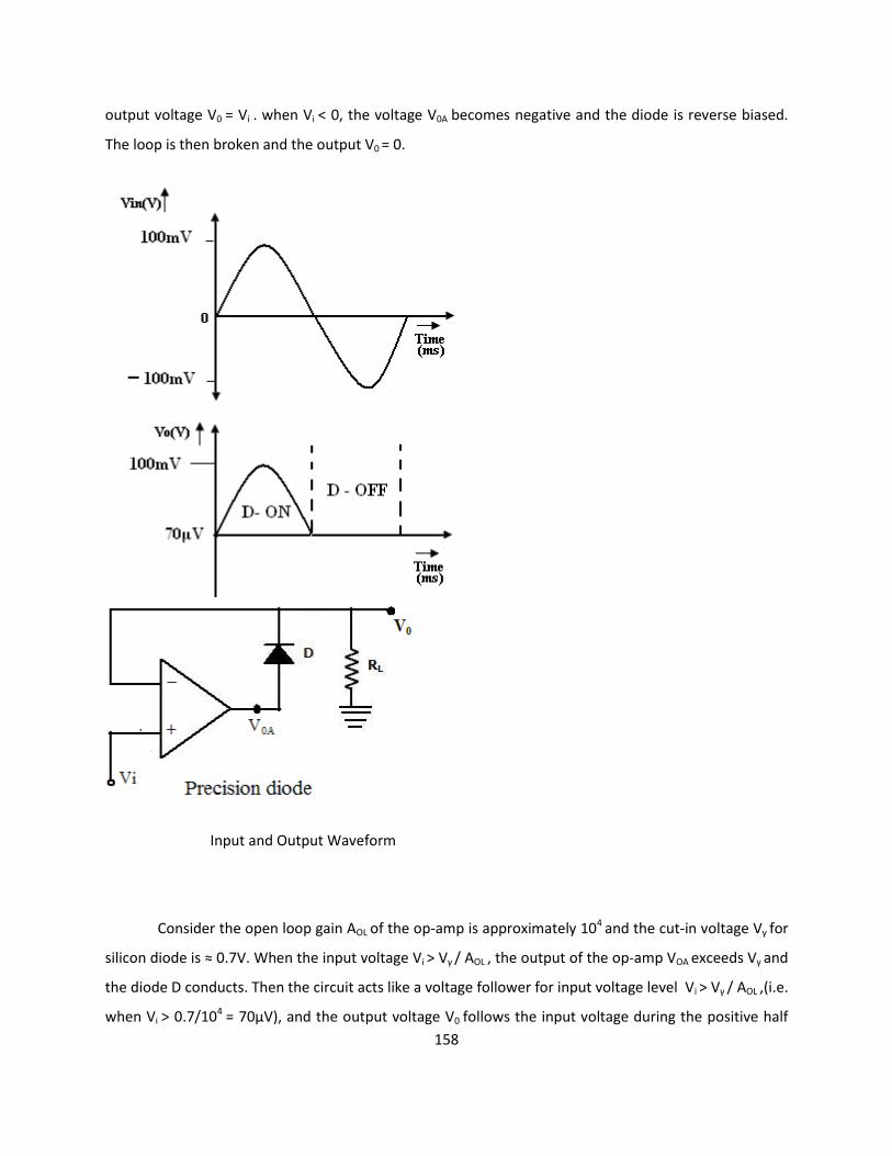
158
output voltage V0 = Vi . when Vi < 0, the voltage V0A becomes negative and the diode is reverse biased.
The loop is then broken and the output V0 = 0.
Input and Output Waveform
Consider the open loop gain AOL of the op-amp is approximately 104 and the cut-in voltage Vγ for
silicon diode is ≈ 0.7V. When the input voltage Vi > Vγ / AOL , the output of the op-amp VOA exceeds Vγ and
the diode D conducts. Then the circuit acts like a voltage follower for input voltage level Vi > Vγ / AOL ,(i.e.
when Vi > 0.7/104 = 70μV), and the output voltage V0 follows the input voltage during the positive half

159
cycle for input voltages higher than 70μV as shown in figure. When Vi is negative or less than Vγ / AOL ,
the output of op-amp VOA becomes negative, and the diode becomes reverse biased. The loop is then
broken, and the op-amp swings down to negative saturation. However, the output terminal is now
isolated from both the input signal and the output of the op-amp terminal thus V0 =0. No current is then
delivered to the load RL except for the small bias current of the op-amp and the reverse saturation
current of the diode.
This circuit is an example of a non-linear circuit, in which linear operation is achieved over the
remaining region (Vi < 0). Since the output swings to negative saturation level when Vi < 0, the circuit is
basically of saturating form. Thus the frequency response is also limited. The precision diodes are used
in half wave rectifier, Full-wave rectifier, peak value detector, clipper and clamper circuits.
It can be observed that the precision diode as shown in figure operated in the first quadrant with Vi > 0
and V0 > 0. The operation in third quadrant can be achieved by connecting the diode in reverse direction.
Half – wave Rectifier:
A non-saturating half wave precision rectifier circuit is shown in figure. When Vi > 0V , the voltage at the
inverting input becomes positive, forcing the output VOA to go negative. This results in forward biasing
the diode D1 and the op-amp output drops only by ≈ 0.7V below the inverting input voltage. Diode D2
becomes reverse biased. The output voltage V0 is zero when the input is positive. When Vi > 0, the op-
amp output VOA becomes positive, forward biasing the diode D2 and reverse biasing the diode D1 . The
circuit then acts like an inverting amplifier circuit with a non-linear diode in the forward path. The gain
of the circuit is unity when Rf = Ri .

160
The circuit operation can mathematically be expressed as

161
V 0 0 when V i > 0
and
V 0
R f
Ri
fffffffV i forV i <0
The voltageV OA at the op @amp output is
V OAt 0.7 forV i > 0V
and
V OAt
R f
Ri
fffffffV i 0.7V forV i < 0V A
The input and output waveforms are shown in figure. The op-amp shown in the circuit must be a high
speed op-amp. This accommodates the abrupt changes in the value of VOA when Vi changes sign and
improves the frequency response characteristics of the circuit.
The advantages of half wave rectifier are it is a precision half wave rectifier and it is a non saturating
one.
The inverting characteristics of the output V0 can be circumvented by the use of an additional inversion
for achieving a positive output.
Full wave Rectifier:
The Full wave Rectifier circuit commonly used an absolute value circuit is shown in figure. The first part
of the total circuit is a half wave rectifier circuit considered earlier in figure. The second part of the
circuit is an inverting.

162
For positive input voltage Vi > 0V and assuming that RF =Ri = R, the output voltage VOA = Vi . The voltage V0
appears as (-) input to the summing op-amp circuit formed by A2 , The gain for the input V’0 is R/(R/2), as

163
shown in figure. The input Vi also appears as an input to the summing amplifier. Then, the net output is
V0 = -Vi -2V’0
= -Vi -2(-Vi ) = Vi
Since Vi > 0V, V’0 will be positive, with its input output characteristics in first quadrant. For negative input
Vi < 0V, the output V’0 of the first part of rectifier circuit is zero. Thus, one input of the summing circuit
has a value of zero. However, Vi is also applied as an input to the summer circuit formed by the op-amp
A2 . The gain for this input id (-R/R) = -1, and hence the output is V0 = -Vi . Since Vi is negative, v0 will be
inverted and will thus be positive. This corresponds to the second quadrant of the circuit.
To summarize the operation of the circuit,
V0 = Vi when Vi < 0V and V0 = Vi for Vi > 0V, and hence V0 = |Vi |
It can be observed that this circuit is of non-saturating form. The input and output waveforms are shown
in the figure.
Peak detector:
Square, Triangular, Sawtooth and pulse waves are typical examples of non-sinusoidal
waveforms. A conventional ac voltmeter cannot be used to measure these sinusoidal waveforms
because it is designed to measure the rms value of the pure sine wave. One possible solution to this
problem is to measure the peak values of the non-sinusoidal waveforms. Peak detector measures the
+ve peak value of the square wave input.
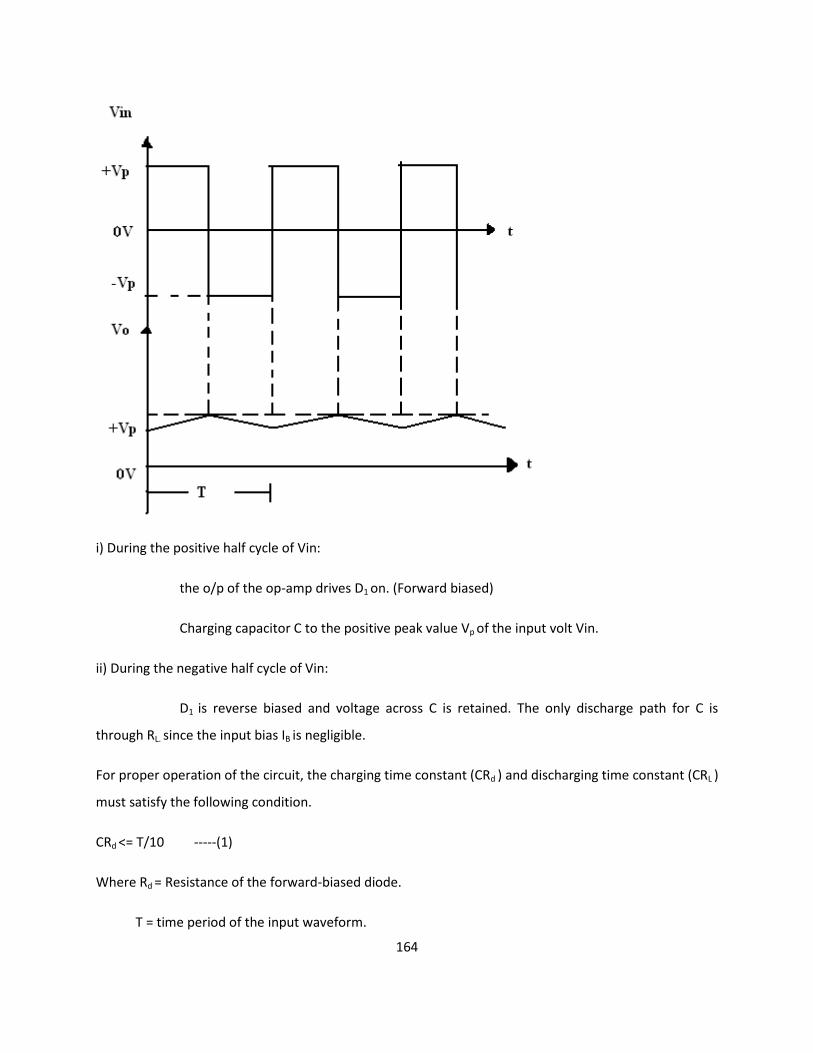
164
i) During the positive half cycle of Vin:
the o/p of the op-amp drives D1 on. (Forward biased)
Charging capacitor C to the positive peak value Vp of the input volt Vin.
ii) During the negative half cycle of Vin:
D1 is reverse biased and voltage across C is retained. The only discharge path for C is
through RL. since the input bias IB is negligible.
For proper operation of the circuit, the charging time constant (CRd ) and discharging time constant (CRL )
must satisfy the following condition.
CRd <= T/10 -----(1)
Where Rd = Resistance of the forward-biased diode.
T = time period of the input waveform.

165
CRL >=10T -----(2)
Where RL = load resistor. If RL is very small so that eqn (2) cannot be satisfied. Use a (buffer) voltage
follower circuit between capacitor C and RL load resistor.
R = is used to protect the op-amp against the excessive discharge currents.
Rcomp = minimizes the offset problems caused by input current
D2 = conducts during the –ve half cycle of Vin and prevents the op-amp from going into negative
saturation.
Note: -ve peak of the input signal can be detected simply by reversing diode D1 and D2 .
Clippers and Clampers:
Waveshaping circuits are commonly used in digital computers and communication such as
TV and FM receiver. Waveshaping technique include clipping and clamping. In op-amp clipper circuits a
rectifier diode may be used to clip off a certain portion of the input signal to obtain a desired o/p
waveform. The diode works as an ideal diode (switch) because when on -> the voltage drop across the
diode is divided by the open loop gain of the op-amp. When off(reverse biased) -> the diode is an open
circuit.
In an op-amp clamper circuits, however a predetermined dc level is deliberately inserted in the o/p volt.
For this reason, the clamper is sometimes called a dc inverter.
Positive and Negative Clipper:
Positive Clipper:
A Circuit that removes positive parts of the input signal can be formed by using an op-
amp with a rectifier diode. The clipping level is determined by the reference voltage Vref, which should
less than the i/p range of the op-amp (Vref < Vin). The Output voltage has the portions of the positive
half cycles above Vref clipped off.
The circuit works as follows:

166
During the positive half cycle of the input, the diode D1 conducts only until Vin = Vref. This happens
because when Vin <Vref, the output volts V0 ‘ of the op-amp becomes negative to device D1 into
conduction when D1 coonducts it closes feedback loop and op-amp operates as a voltage follower. (i.e)
Output V0 follows input until Vin = Vref.
When Vin > Vref => the V’0 becomes +ve to derive D1 into off. It open the feedback loop and op-amp
operates open loop. When Vin drops below Vref (Vin<Vref) the o/p of the op-amp V’0 again becomes –ve
to device D1 into conduction. It closed the f/b. (o/p follows the i/p). Thus diode D1 is on for vin<Vref (o/p
follows the i/p) and D1 is off for Vin>Vref. The op-amp alternates between open loop (off) and closed
loop operation as the D1 is turned off and on respectively. For this reason the op-amp used must be high
speed and preferably compensated for unity gain.

167

168
Ex: for high speed op-amp HA 2500, LM310, μA 318. In addition the difference input voltage (Vid=high)
is high during the time when the feedback loop is open (D1 is off) hence an op-amp with a high
difference input voltage is necessary to prevent input breakdown. If Rp (pot) is connected to –VEE instead
of +Vcc, the ref voltage Vref will be negative (Vref = -ve). This will cause the entire o/p waveform above
–Vref to be clipped off.
Negative Clipper:
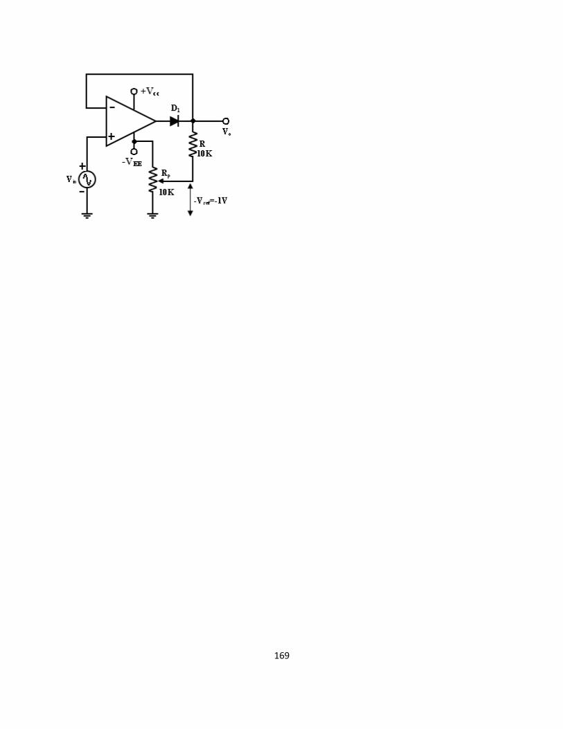
169
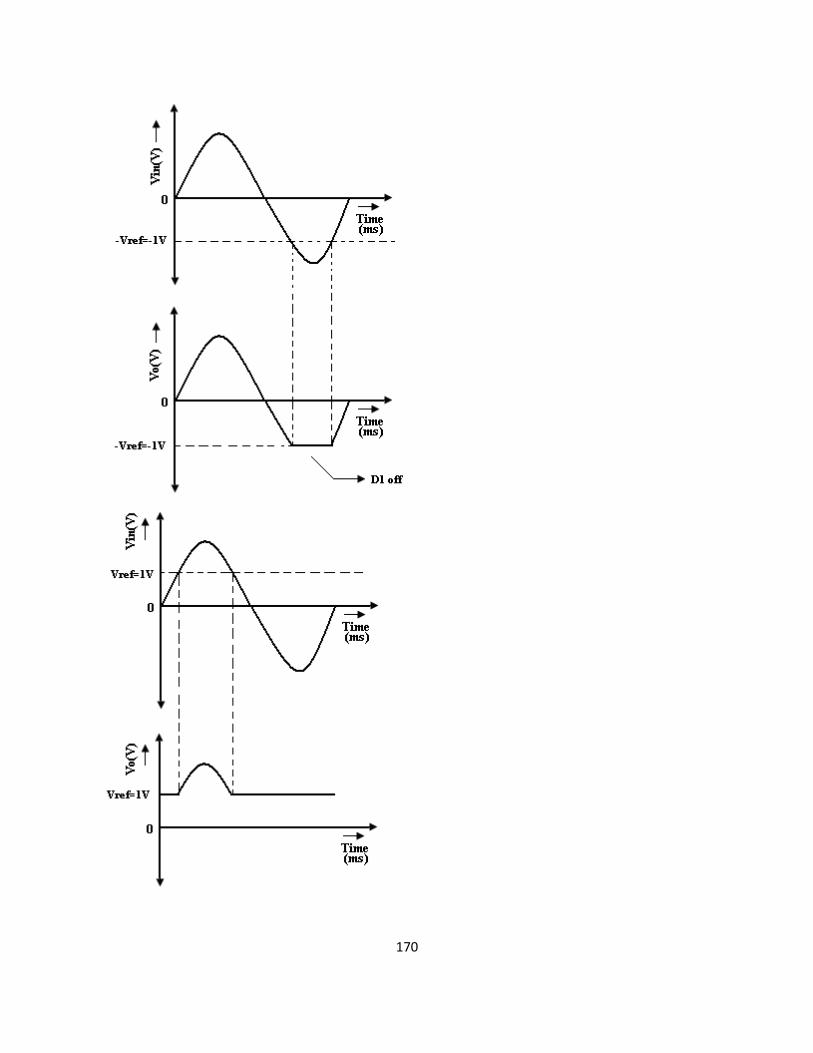
170

171
The positive clipper is converted into a –ve clipper by simply reversing diode D1 and changing the
polarity of Vref voltage. The negative clipper -> clips off the –ve parts of the input signal below the
reference voltage. Diode D1 conducts -> when Vin > -Vref and therefore during this period o/p volt V0
follows the i/p volt Vin. The –Ve portion of the output volt below –Vref is clipped off because (D1 is off)
Vin<-Vref. If –Vref is changed to –Vref by connecting the potentiometer Rp to the +Vcc, the V0 below
+Vref will be clipped off. The diode D1 must be on for Vin > Vref and off for Vin.
Positive and Negative Clampers:
In clamper circuits a predetermined dc level is added to the output voltage. (or) The output is clamped
to a desired dc level.
1. If the clamped dc level is +ve, the clamper is positive clamper
2. If the clamped dc level is –ve, the clamper is negative clamper.
Other equivalent terms used for clamper are dc inserter or restorer. Inverting and Non-Inverting that
use this technique.

172

173
Capacitor:
The Value of the capacitors in these circuits depends on different input rates and pulse widths.
1. In both circuits the dc level added to the o/p voltage is approximately equal to Vcc/2.
2. This +ve fixed dc level is needed to obtain a maximum undistored symmetrical sine wave.
Peak clamper circuit: Input and output waveform with +Vref:
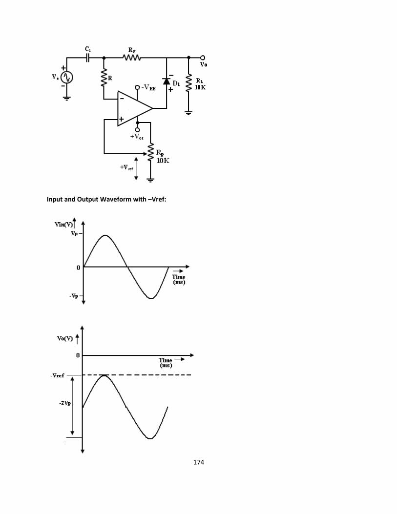
174
Input and Output Waveform with –Vref:

175
In this circuit, the input waveform peak is clamped at Vref. For this reason, the circuit is
called the peak clamper.
First consider the input voltage Vref at the (+) input: since this volt is +ve, V’0 is also +ve which forward
biases D1 . This closed the feedback loop.
Voltage Vin at the (-) input: During its –ve half cycle, diode D1 conducts, charging c; to the –ve peak value
of Vp . During the +ve half cycle, diode D1 in reverse biased. Since this voltage Vp is in series with the +ve
peak volt Vp the o/p volt V0 = 2 Vp. Thus the nett o/p is Vref plus 2 Vp. so the –ve peak of 2 Vp is at Vref.
For precision clamping, CiRd << T/2
Where Rd = resistance of diode D1 when it is forward biased.
T = time period of the input waveform.
Resistor r => is used to protect the op-amp against excessive discharge currents from capacitor Ci
especially when the dc supply voltages are switched off. A +ve peak clamping is accomplished by
reversing D1 and using –ve reference voltage (-Vref).
Note:
Inv and Non-Inv clamper – Fixed dc level
Peak clamper – Variable dc level
Active filters:
Another important field of application using op-amp.
Filters and Oscillators:
An electric filter is often a frequency selective circuit that passes a specified band of frequencies
and blocks or alternates signal and frequencies outside this band.
Filters may be classified as
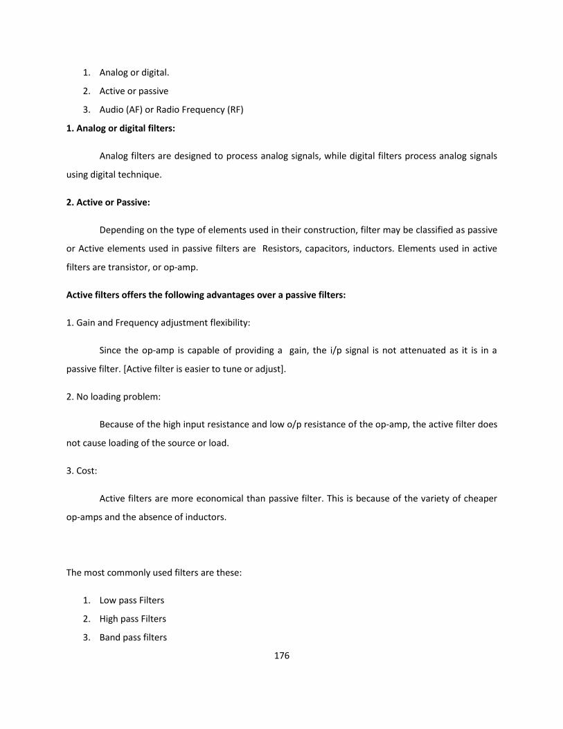
176
1. Analog or digital.
2. Active or passive
3. Audio (AF) or Radio Frequency (RF)
1. Analog or digital filters:
Analog filters are designed to process analog signals, while digital filters process analog signals
using digital technique.
2. Active or Passive:
Depending on the type of elements used in their construction, filter may be classified as passive
or Active elements used in passive filters are Resistors, capacitors, inductors. Elements used in active
filters are transistor, or op-amp.
Active filters offers the following advantages over a passive filters:
1. Gain and Frequency adjustment flexibility:
Since the op-amp is capable of providing a gain, the i/p signal is not attenuated as it is in a
passive filter. [Active filter is easier to tune or adjust].
2. No loading problem:
Because of the high input resistance and low o/p resistance of the op-amp, the active filter does
not cause loading of the source or load.
3. Cost:
Active filters are more economical than passive filter. This is because of the variety of cheaper
op-amps and the absence of inductors.
The most commonly used filters are these:
1. Low pass Filters
2. High pass Filters
3. Band pass filters
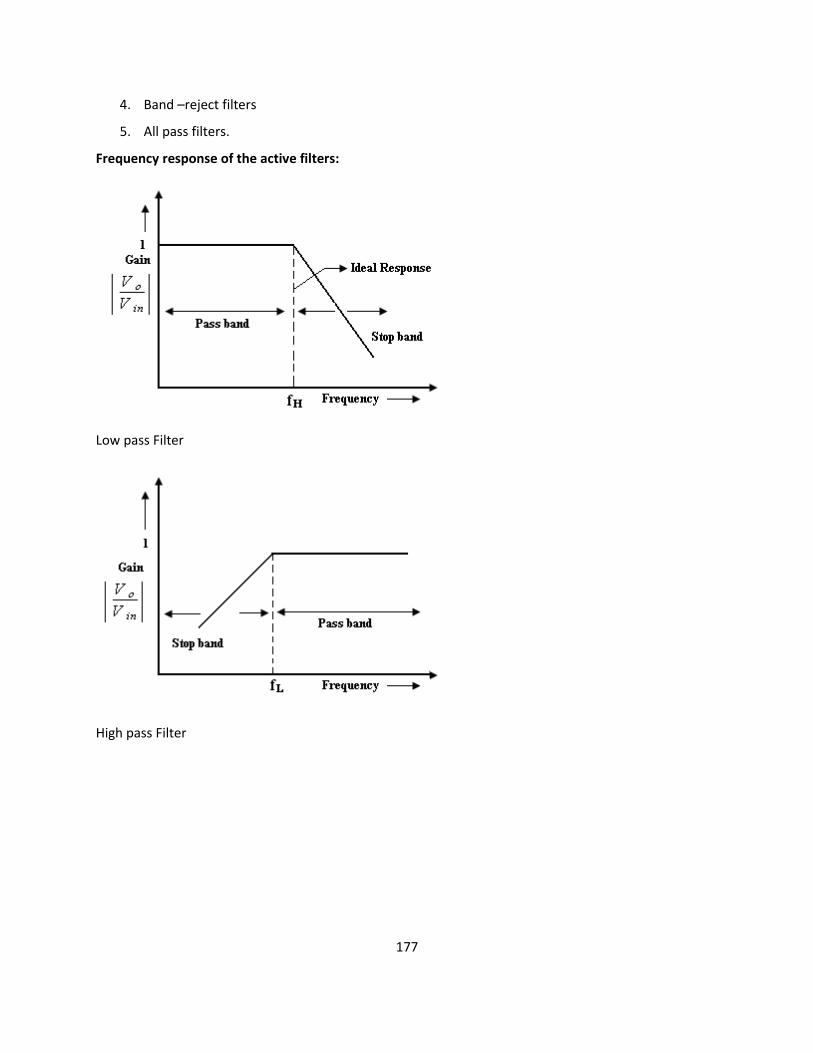
177
4. Band –reject filters
5. All pass filters.
Frequency response of the active filters:
Low pass Filter
High pass Filter
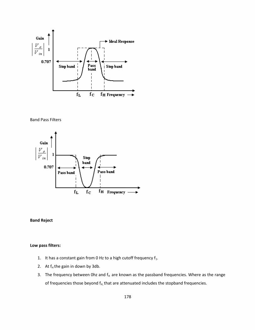
178
Band Pass Filters
Band Reject
Low pass filters:
1. It has a constant gain from 0 Hz to a high cutoff frequency f1.
2. At fH the gain in down by 3db.
3. The frequency between 0hz and fH are known as the passband frequencies. Where as the range
of frequencies those beyond fH, that are attenuated includes the stopband frequencies.

179
4. Butterworth, clebyshev and cauer filter are some of the most commonly used practical filters.
5. The key characteristics of the butter worth filter is that it has a flat pass band as well as stop
band. For this reason, it is sometimes called a flat-flat filters.
6. Chebyshev filter -> has a ripple pass band & flat stop band.
7. Causer Filter -> has a ripple pass band & ripple stopband. It gives best stopband response among
the three.
High pass filter:
High pass filter with a stop band 0<f< f L and a pass band f> f L
fL -> low cut off frequency
f -> operating frequency.
Band pass filter:
It has a pass band between 2 cut off frequencies fH and fL where fH > fL and two, stop bands :
0<f< fL and f > fH between the band pass filter (equal to fH - fL .
Band –reject filter: (Band stop or Band elimination)
It performs exactly opposite to the band pass. It has a band stop between 2 cut-off frequency fL
and fH and 2 passbands: 0<f< fL and f> fH
fC -> center frequency.
Note:
The actual response curves of the filters in the stopband either R or S or both with R in
frequencies.
The rate at which the gain of the filter changes in the stopband is determined by the order of
the filter.
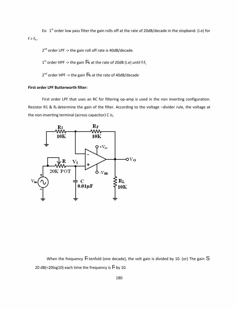
180
Ex: 1st order low pass filter the gain rolls off at the rate of 20dB/decade in the stopband. (i.e) for
f > fH .
2nd order LPF -> the gain roll off rate is 40dB/decade.
1st order HPF -> the gain Rs at the rate of 20dB (i.e) until f:fL
2nd order HPF -> the gain Rs at the rate of 40dB/decade
First order LPF Butterworth filter:
First order LPF that uses an RC for filtering op-amp is used in the non inverting configuration.
Resistor R1 & Rf determine the gain of the filter. According to the voltage –divider rule, the voltage at
the non-inverting terminal (across capacitor) C is,
When the frequency R tenfold (one decade), the volt gain is divided by 10. (or) The gain S
20 dB(=20log10) each time the frequency is R by 10.

181
Hence the rate at which the gain rolls off fH = 20 dB or 6dB/octatve (twofold R in frequency).
The frequency f = fH is called the cut off frequency because the gain of the filter at this frequency is
down by 3 dB(=20 log 0.70)
Filter Origin:
A LPF can be designed by implementing the following steps.
1. Choose a value of high cut off frequency fH .
2. Select a value of C less than or equal to 1μf.
3. Choose the value of R suing, R1
2 fH
C
ffffffffffffffffffff
4. Finally select values of R1 and RF dependent on the desired passband gain AF using,
AF 1RF
R1
ffffffff
Frequency Scaling:
Once a filter is designed, these may sometimes be a need to change its cutoff frequency.
Convertion of original cutoff frequency fH to a new cut off frequency fH ‘ is called
frequency scaling.
To change a high cutoff frequency multiply R or C, but not both by the ratio of
Original cutoff frequency
------------------------------------------------
New cut off frequency
And f’H R or f’H C and then calculate fH .

182
Second order LP Butterworth filter:
A second order LPF having a gain 40dB/decade in stop band. A First order LPF can be
converted into a II order type simply by using an additional RC network.
The gain of the II order filter is set by R1 and RF, while the high cut off frequency fH is determined by
R2,C2,R3 and C3.
f
H
1
2 R2 R3 C2 C3qwwwwwwwwwwwwwwwwwwwwwwwwwwwwwwwwwwwwwwwwwwwwwwwwwwwwwwwwwwwwwwwwwwwwwwwwwwwwwwwwwwwwwwwwwwwwwwwwwwwwwwwwwwwwwwwwwwwwwwwwwwwwwwwwwwwwwwwwwwwwwwwwwwwwwwwwwwwwwwwwwwwwwwwwwwwwwwwwwwwwww
ffffffffffffffffffffffffffffffffffffffffffff@@@1
` a

183
This above fig transferred into S domain.
In this circuit all the components and the circuit parameters are expressed in the S-domain where S = j .
Writing Kirchoff’s current law at node VA (S) .
I1 = I2 + I3
The denominator quadratic in the gain (V0/Vin) eqn must have two real and equal roots. This means
that
For a second-order LP Butterworth response, the volt gain magnitude eqn is,
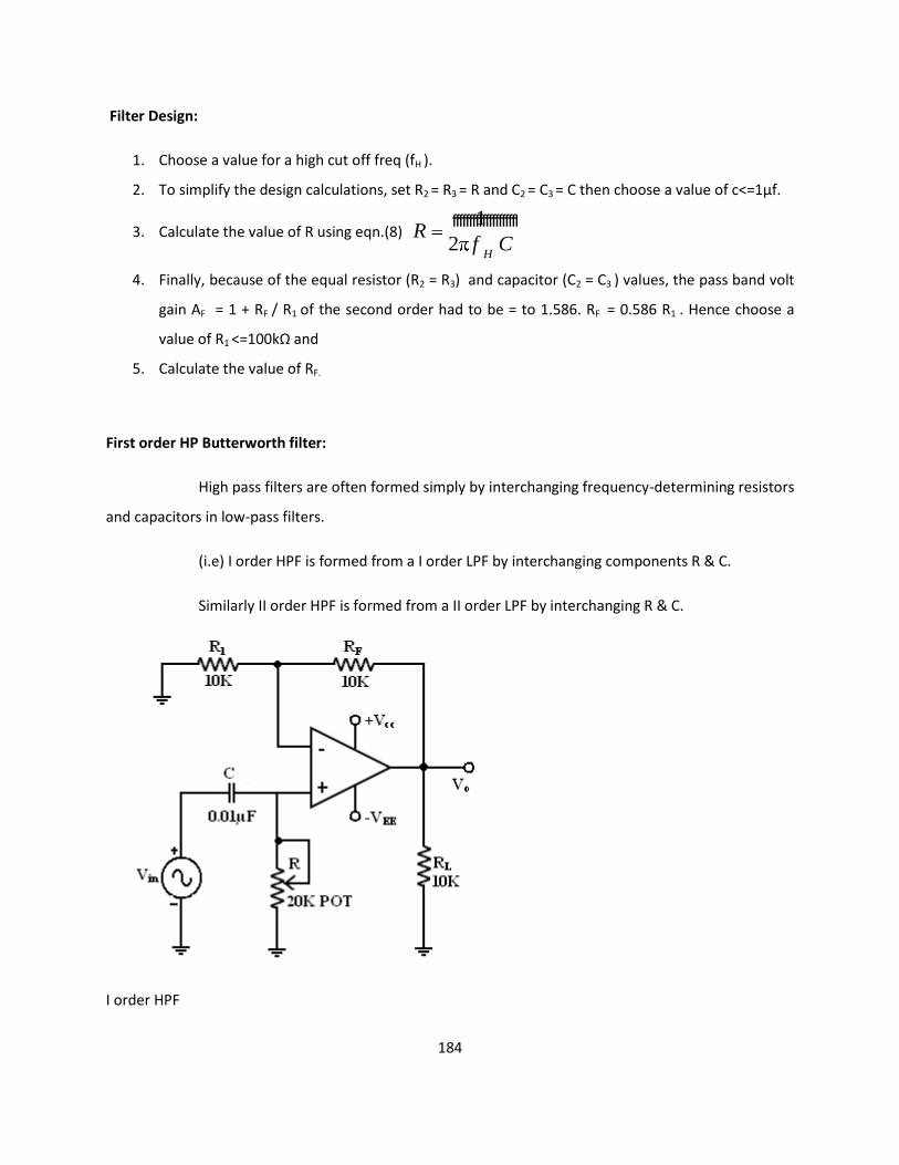
184
Filter Design:
1. Choose a value for a high cut off freq (fH ).
2. To simplify the design calculations, set R2 = R3 = R and C2 = C3 = C then choose a value of c<=1μf.
3. Calculate the value of R using eqn.(8) R1
2 fH
C
ffffffffffffffffffff
4. Finally, because of the equal resistor (R2 = R3) and capacitor (C2 = C3 ) values, the pass band volt
gain AF = 1 + RF / R1 of the second order had to be = to 1.586. RF = 0.586 R1 . Hence choose a
value of R1 <=100kΩ and
5. Calculate the value of RF.
First order HP Butterworth filter:
High pass filters are often formed simply by interchanging frequency-determining resistors
and capacitors in low-pass filters.
(i.e) I order HPF is formed from a I order LPF by interchanging components R & C.
Similarly II order HPF is formed from a II order LPF by interchanging R & C.
I order HPF

185
Here I order HPF with a low cut off frequency of fL. This is the frequency at which the
magnitude of the gain is 0.707 times its passband value.
Here all the frequencies higher than fL are passband frequencies.
For the first order high pass filter, the output voltage is,
Note: Design and Frequency scaling procedure of the LPF are also applicable to the HPF.
Second – order High Pass Butterworth Filter:
I order Filter, II order HPF can be formed from a II order LPF by interchanging the
frequency – determine resistors and capacitors.

186
II order HPF
The Volt gain magnitude eqn of the II order HPF is as follows,

187
UNIT III ANALOG MULTIPLIER AND PLL
555 Timer circuit – Functional block – Characteristics and applications; 566 – Voltage controlled
oscillator circuit; 565 – Phase lock loop circuit functioning and applications – Analog multiplier
ICs.
Basic Block Diagram of a PLL
Forward path
fIN fOUT
Input
frequency
Feedback path
phase locked loop construction and operation:

188
The PLL consists of i) Phase detector ii) LPF iii) VCO. The phase detector or comparator compares the
input frequency fIN with feedback frequency fOUT.
The output of the phase detector is proportional to the phase difference between fIN & fOUT. The
output of the phase detector is a dc voltage & therefore is often referred to as the error voltage.
The output of the phase detector is then applied to the LPF, which removes the high frequency
noise and produces a dc level. This dc level in turn, is input to the VCO.
The output frequency of VCO is directly proportional to the dc level. The VCO frequency is compared
with input frequency and adjusted until it is equal to the input frequencies.
PLL goes through 3 states, i) free running ii) Capture iii) Phase lock.
Before the input is applied, the PLL is in free running state. Once the input frequency is applied the VCO
frequency starts to change and PLL is said to be in the capture mode. The VCO frequency continuous to
change until it equals the input frequency and the PLL is in phase lock mode. When Phase locked, the
loop tracks any change in the input frequency through its repetitive action. If an input signal vs of
frequency fs is applied to the PLL, the phase detector compares the phase and frequency of the incoming
signal to that of the output vo of the VCO. If the two signals differ in frequency of the incoming signal to
that of the output vo of the VCO. If the two signals differ in frequency and/or phase, an error voltage ve is
generated.
The phase detector is basically a multiplier and produces the sum (fs + fo) and difference (fs - fo)
components at its output. The high frequency component (fs + fo) is removed by the low pass filter and
the difference frequency component is amplified then applied as control voltage vc to VCO. The signal vc
shifts the VCO frequency in a direction to reduce the frequency difference between fs and fo. Once this
action starts, we say that the signal is in the capture range. The VCO continues to change frequency till
its output frequency is exactly the same as the input signal frequency. The circuit is then said to be
locked. Once locked, the output frequency fo of VCO is identical to fs except for a finite phase difference
φ. This phase difference φ generates a corrective control voltage vc to shift the VCO frequency from f0 to
fs and thereby maintain the lock. Once locked, PLL tracks the frequency changes of the input signal.
Thus, a PLL goes through three stages (i) free running, (ii) capture and (iii) locked or tracking.
Capture range: the range of frequencies over which the PLL can acquire lock with an input signal is called
the capture range. This parameter is also expressed as percentage of fo.

189
Pull-in time: the total time taken by the PLL to establish lock is called pull-in time. This depends on the
initial phase and frequency difference between the two signals as well as on the overall loop gain and
loop filter characteristics.
(a) Phase Detector:
Phase detector compares the input frequency and VCO frequency and generates DC voltage i.e.,
proportional to the phase difference between the two frequencies. Depending on whether the
analog/digital phase detector is used, the PLL is called either an analog/digital type respectively. Even
though most monolithic PLL integrated circuits use analog phase detectors.
Ex for Analog: Double-balanced mixer
Ex for Digital: Ex-OR, Edge trigger, monolithic Phase detector.
Ex-OR Phase Detector:
This uses an exclusive OR gate. The output of the Ex-OR gate is high only when fIN or fOUT is high.
The DC output voltage of the Ex-OR phase detector is a function of the phase difference between its two
outputs. The maximum dc output voltage occurs when the phase difference is Π radians or 180 degrees.
The slope of the curve between 0 or Π radians is the conversion gain kp of the phase detector for eg; if
the Ex-OR gate uses a supply voltage Vcc = 5V, the conversion gain Kp is
KP = V5
= 1.59V / RAD
Edge Triggered Phase Detector:

190
Advantages of Edge Triggered Phase Detector over Ex-OR are
i) The dc output voltage is linear over 2Π radians or 360 degrees, but in Ex-OR it is Π radians or 180
degrees.
ii) Better Capture, tracking & locking characteristics.
Edge triggered type of phase detector using RS Flip – Flop. It is formed from a pair of cross coupled NOR
gates.
RS FF is triggered, i.e, the output of the detector changes its logic state on the positive edge of the
inputs fIN & fOUT
Monolithic Phase detector:
It consists of 2 digital phase detector, a charge pump and an amplifier.
Phase detector 1 is used in applications that require zero frequency and phase difference at lock.
Phase detector 2, if quadrature lock is desired, when detector 1 is used in the main loop, detector
can also be used to indicate whether the main loop is in lock or out of lock.
R Reference
V Variable or 0feedback input
PU Pump Up signal
PDPump Down signal
UF Up frequency output signal
DF Down frequency output signal
(b) Low – Pass filter:

191
The function of the LPF is to remove the high frequency components in the output of the phase
detector and to remove the high frequency noise. LPF controls the characteristics of the phase locked
loop. i.e, capture range, lock ranges, bandwidth
Lock range(Tracking range):
The lock range is defined as the range of frequencies over which the PLL system follows the
changes in the input frequency fIN.
Capture range:
Capture range is the frequency range in which the PLL acquires phase lock. Capture range
is always smaller than the lock range.
Filter Bandwidth:
Filter Bandwidth is reduced, its response time increases. However reduced Bandwidth reduces
the capture range of the PLL. Reduced Bandwidth helps to keep the loop in lock through
momentary losses of signal and also minimizes noise.
(c) Voltage Controlled Oscillator (VCO):
The third section of PLL is the VCO; it generates an output frequency that is directly proportional
to its input voltage. The maximum output frequency of NE/SE 566 is 500 Khz.
fIN fOUT
Input
frequency

192
Feedback path and optional divider:
Most PLLs also include a divider between the oscillator and the feedback input to the phase
detector to produce a frequency synthesizer. A programmable divider is particularly useful in
radio transmitter applications, since a large number of transmit frequencies can be produced from
a single stable, accurate, but expensive, quartz crystal–controlled reference oscillator.
Some PLLs also include a divider between the reference clock and the reference input to the
phase detector. If this divider divides by M, it allows the VCO to multiply the reference
frequency by N / M. It might seem simpler to just feed the PLL a lower frequency, but in some
cases the reference frequency may be constrained by other issues, and then the reference divider
is useful. Frequency multiplication in a sense can also be attained by locking the PLL to the 'N'th
harmonic of the signal.
Equations:
The equations governing a phase-locked loop with an analog multiplier as the phase detector
may be derived as follows. Let the input to the phase detector be xc(t) and the output of the
voltage-controlled oscillator (VCO) is xr(t) with frequency ωr(t), then the output of the phase
detector xm(t) is given by
the VCO frequency may be written as a function of the VCO input y(t) as
where gv is the sensitivity of the VCO and is expressed in Hz / V.

193
Hence the VCO output takes the form
where
The loop filter receives this signal as input and produces an output
xf(t) = Ffilter(xm(t))
where FFilter is the operator representing the loop filter transformation.
When the loop is closed, the output from the loop filter becomes the input to the VCO thus
y(t) = xf(t) = Ffilter(xm(t))
We can deduce how the PLL reacts to a sinusoidal input signal:
xc(t) = Acsin(ωct).
The output of the phase detector then is:
This can be rewritten into sum and difference components using trigonometric identities:
As an approximation to the behaviour of the loop filter we may consider only the difference
frequency being passed with no phase change, which enables us to derive a small-signal model
of the phase-locked loop. If we can make , then the can be approximated by its

194
argument resulting in: . The phase-locked loop is said to be
locked if this is the case.
CONTROL SYSTEM ANALYSIS/ CLOSED LOOP ANALYSIS OF PLL
Phase locked loops can also be analyzed as control systems by applying the Laplace transform.
The loop response can be written as:
Where
θo is the output phase in radians
θi is the input phase in radians
Kp is the phase detector gain in volts per radian
Kv is the VCO gain in radians per volt-second
F(s) is the loop filter transfer function (dimensionless)
The loop characteristics can be controlled by inserting different types of loop filters. The
simplest filter is a one-pole RC circuit. The loop transfer function in this case is:
The loop response becomes:
This is the form of a classic harmonic oscillator. The denominator can be related to that of a
second order system:

195
Where
ζ is the damping factor
ωn is the natural frequency of the loop
For the one-pole RC filter,
The loop natural frequency is a measure of the response time of the loop, and the damping factor
is a measure of the overshoot and ringing. Ideally, the natural frequency should be high and the
damping factor should be near 0.707 (critical damping). With a single pole filter, it is not
possible to control the loop frequency and damping factor independently. For the case of critical
damping,
A slightly more effective filter, the lag-lead filter includes one pole and one zero. This can be
realized with two resistors and one capacitor. The transfer function for this filter is
This filter has two time constants

196
τ1 = C(R1 + R2)
τ2 = CR2
Substituting above yields the following natural frequency and damping factor
The loop filter components can be calculated independently for a given natural frequency and
damping factor
Real world loop filter design can be much more complex eg using higher order filters to reduce
various types or source of phase noise.
Applications of PLL:
The PLL principle has been used in applications such as FM stereo decoders, motor speed control,
tracking filters, FM modulation and demodulation, FSK modulation, Frequency multiplier, Frequency
synthesis etc.,
Example PLL ICs:

197
560 series (560, 561, 562, 564, 565 & 567)
VOLTAGE CONTROLLED OSCILLATOR:
A common type of VCO available in IC form is Signetics NE/SE566. The pin configuration and basic block
diagram of 566 VCO are shown in figures below.
Referring to the circuit in the above figure, the capacitor c1 is linearly charged or discharged by a
constant current source/sink. The amount of current can be controlled by changing the voltage vc
applied at the modulating input (pin 5) or by changing the timing resistor R1 external to the IC chip. The
voltage at pin 6 is held at the same voltage as pin 5. Thus, if the modulating voltage at pin 5 is increased,

198
the voltage at pin 6 also increases, resulting in less voltage across R1 and thereby decreasing the
charging current.
The voltage across the capacitor C1 is applied to the inverting input terminal of Schmitt trigger
via buffer amplifier. The output voltage swing of the Schmitt trigger is designed to Vcc and 0.5 Vcc. If Ra =
Rb in the positive feedback loop, the voltage at the non-inverting input terminal of Schmitt trigger swings
from 0.5 Vcc to 0.25 Vcc. When the voltage on the capacitor c1 exceeds 0.5 Vcc during charging, the output
of the Schmitt trigger goes LOW (0.5 Vcc). The capacitor now discharges and when it is at 0.25 Vcc, the
output of Schmitt trigger goes HIGH (Vcc). Since the source and sink currents are equal, capacitor charges
and discharges for the same amount of time. This gives a triangular voltage waveform across c1 which is
also available at pin 4. The square wave output of the Schmitt trigger is inverted by buffer amplifier at
pin 3. The output waveforms are shown near the pins 4 and 3.
The output frequency of the VCO can be given as follows:
where V+ is Vcc.
The output frequency of the VCO can be changed either by (i) R1, (ii) c1 or (iii) the voltage vc at
the modulating input terminal pin 5. The voltage vc can be varied by connecting a R1R2 circuit as shown
in the figure below. The components R1and c1 are first selected so that VCO output frequency lies in the
centre of the operating frequency range. Now the modulating input voltage is usually varied from 0.75
Vcc to Vcc which can produce a frequency variation of about 10 to 1.
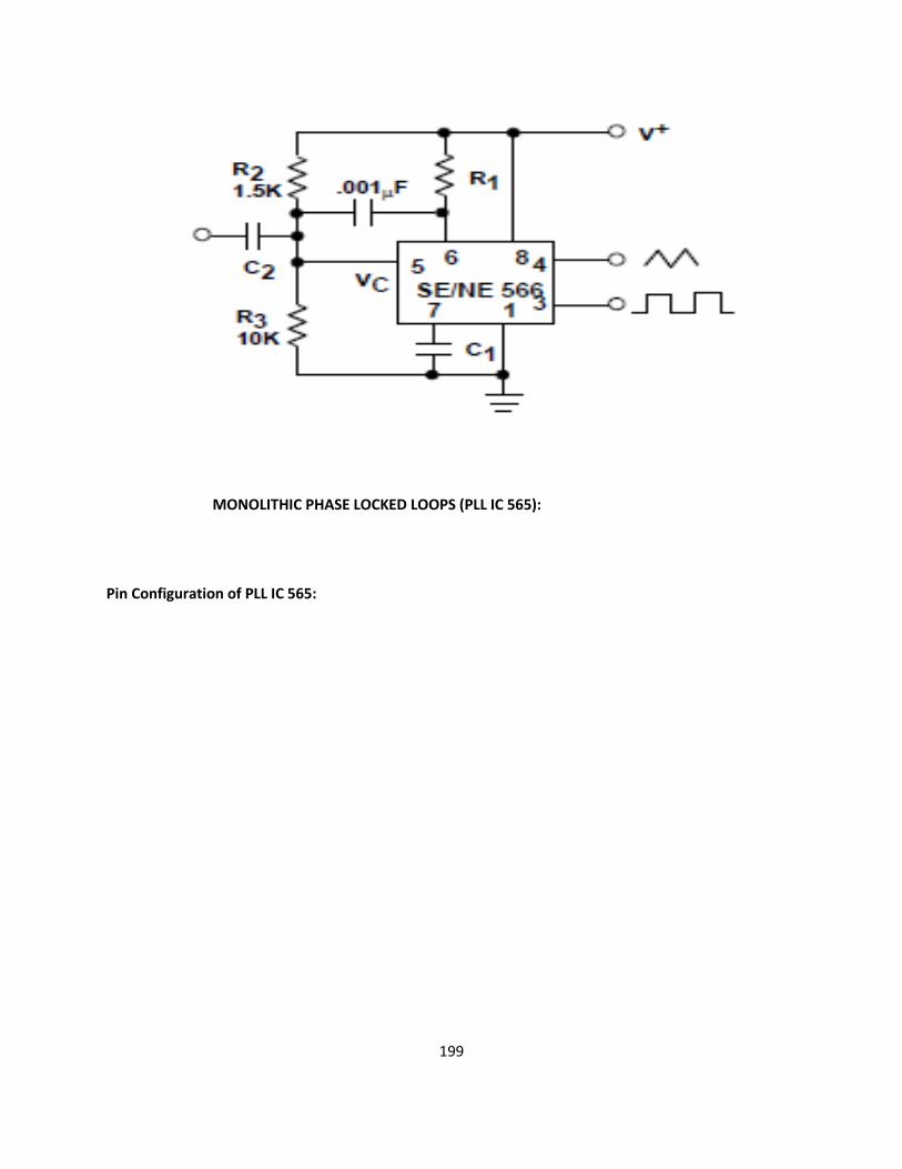
199
MONOLITHIC PHASE LOCKED LOOPS (PLL IC 565):
Pin Configuration of PLL IC 565:

200
Basic Block Diagram Representation of IC 565

201
The signetics NE/SE 560 series is monolithic phase locked loops. The SE/NE 560, 561, 562, 564,
565 & 567 differ mainly in operating frequency range, poser supply requirements & frequency &
bandwidth adjustment ranges. The important electrical characteristics of the 565 PLL are,
Operating frequency range: 0.001Hz to 500 Khz.
Operating voltage range: ±6 to ±12v
Input level required for tracking: 10mv rms min to 3 Vpp max
Input impedance: 10 K ohms typically.
Output sink current: 1mA
Output source current: 10 mA
The center frequency of the PLL is determined by the free running frequency of the VCO, which is given
by
fOUT =114
2.1
CR HZ------------(1)
where R1&C1 are an external resistor & a capacitor connected to pins 8 & 9.
The VCO free-running frequency fOUT is adjusted externally with R1 & C1 to be at the center of the
input frequency range.
C1 can be any value, R1 must have a value between 2 k ohms and 20 K ohms.
Capacitor C2 connected between 7 & +V.
The filter capacitor C2 should be large enough to eliminate variations in the demodulated output
voltage in order to stabilize the VCO frequency.
The lock range fL & capture range fc of PLL is given by,
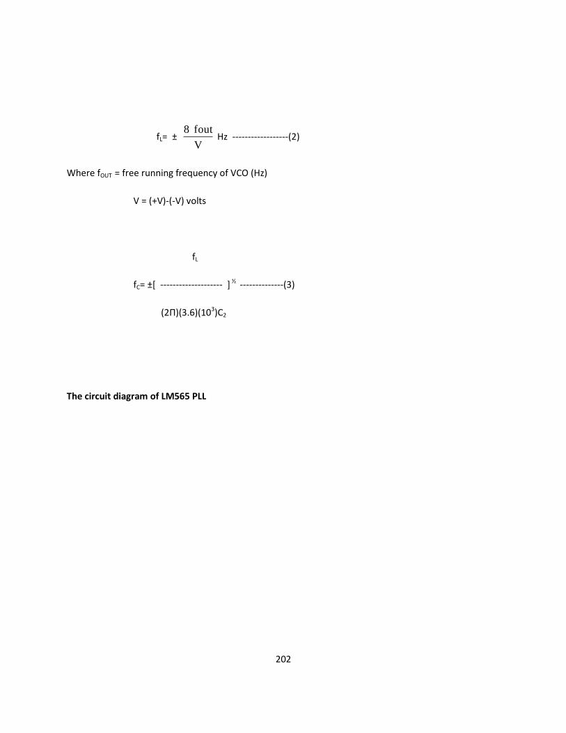
202
fL= ± V
fout 8 Hz ------------------(2)
Where fOUT = free running frequency of VCO (Hz)
V = (+V)-(-V) volts
fL
fC= ±[ -------------------- ] ½ --------------(3)
(2Π)(3.6)(103)C2
The circuit diagram of LM565 PLL

203
Monolithic PLL IC 565 applications:
The output from a PLL system can be obtained either as the voltage signal vc(t) corresponding to the
error voltage in the feedback loop, or as a frequency signal at VCO output terminal. The voltage output
is used in frequency discriminator applications whereas the frequency output is used in signal
conditioning, frequency synthesis or clock recovery applications.
Consider the case of voltage output. When PLL is locked to an input frequency, the error voltage vc(t) is
proportional to (fs-fo). If the input frequency is varied as in the case of FM signal, vc will also vary in order
to maintain the lock. Thus the voltage output serves as a frequency discriminator which converts the
input frequency changes to voltage changes.
In the case of frequency output, if the input signal is comprised of many frequency components
corrupted with noise and other disturbances, the PLL can be made to lock, selectively on one particular
frequency component at the input. The output of VCO would then regenerate that particular frequency
(because of LPF which gives output for beat frequency) and attenuate heavily other frequencies. VCO
output thus can be used for regenerating or reconditioning a desired frequency signal (which is weak
and buried in noise) out of many undesirable frequency signals.

204
Some of the typical applications of PLL are discussed below.
(i)Frequency Multiplier:
Frequency divider is inserted between the VCO & phase comparator. Since the output of the divider
is locked to the fIN, VCO is actually running at a multiple of the input frequency.
The desired amount of multiplication can be obtained by selecting a proper divide-by-N network,
where N is an integer.
(ii)Frequency Shift Keying (FSK) demodulator:
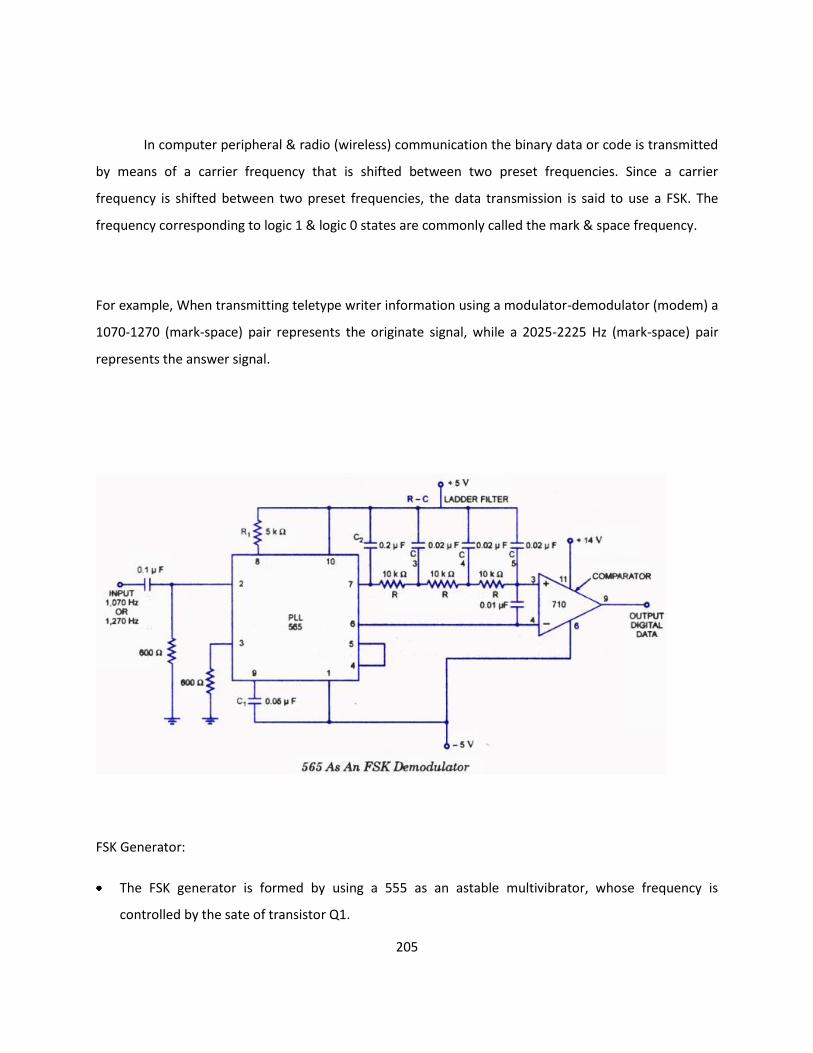
205
In computer peripheral & radio (wireless) communication the binary data or code is transmitted
by means of a carrier frequency that is shifted between two preset frequencies. Since a carrier
frequency is shifted between two preset frequencies, the data transmission is said to use a FSK. The
frequency corresponding to logic 1 & logic 0 states are commonly called the mark & space frequency.
For example, When transmitting teletype writer information using a modulator-demodulator (modem) a
1070-1270 (mark-space) pair represents the originate signal, while a 2025-2225 Hz (mark-space) pair
represents the answer signal.
FSK Generator:
The FSK generator is formed by using a 555 as an astable multivibrator, whose frequency is
controlled by the sate of transistor Q1.

206
In other words, the output frequency of the FSK generator depends on the logic state of the digital
data input.
150 Hz is one the standards frequencies at which the data are commonly transmitted.
When the input is logic 1, the transistor Q1 is off. Under the condition, 555 timer works in its normal
mode as an astable multivibrator i.e., capacitor C charges through RA & RB to 2/3 Vcc & discharges
through RB to 1/3 Vcc.
Thus capacitor C charges & discharges between 2/3 Vcc & 1/3 Vcc as long as the input is logic 1.
The frequency of the output waveform is given by,
1.45
fo=--------------- = 1070 Hz (mark frequency)
(RA +2RB)C
When the input is logic 0, (Q1 is ON saturated) which inturn connects the resistance Rc across RA.
This action reduces the charging time of capacitor C1 increases the output frequency, which is given
by,
1.45
fo= ------------------ = 1270 Hz (space frequency)
(RA || RC+2 RB)C
By proper selection of resistance Rc, this frequency is adjusted to equal the space frequency of 1270
Hz. The difference between the FSK signals of 1070 Hz & 1270 Hz is 200 Hz, this difference is called
“frequency shift”.
The output 150 Hz can be made by connecting a voltage comparator between the output of the
ladder filter and pin 6 of PLL.
The VCO frequency is adjusted with R1 so that at fIN = 1070 Hz.
FSK Demodulator:

207
The output of 555 FSK generator is applied to the 565 FSK demodulator.
Capacitive coupling is used at the input to remove dc line.
At the input of 565, the loop locks to the input frequency & tracks it between the 2 frequencies.
R1 & C1 determine the free running frequency of the VCO, 3 stage RC ladder filter is used to remove
the carrier component from the output.
In digital data communication and computer peripheral, binary data is transmitted by means of a carrier
frequency which is shifted between two preset frequencies. This type of data transmission is called
frequency shift keying (FSK) technique. The binary data can be retrieved using FSK demodulator. The
figure below shows FSK demodulator using PLL for tele-typewriter signals of 1070 Hz and 1270 Hz. As
the signal appears at the input, the loop locks to the input frequency and tracks it between the two
frequencies with a corresponding dc shift at the output. A three stage filter removes the carrier
component and the output signal is made logic compatible by a voltage comparator.
(iii)AM Demodulation:

208
A PLL may be used to demodulate AM signals as shown in the figure below. The PLL is locked to the
carrier frequency of the incoming AM signal. The output of VCO which has the same frequency as the
carrier, but unmodulated is fed to the multiplier. Since VCO output is always 900 before being fed to the
multiplier. This makes both the signals applied to the multiplier and the difference signals, the
demodulated output is obtained after filtering high frequency components by the LPF. Since the PLL
responds only to the carrier frequencies which are very close to the VCO output, a PLL AM detector
exhibits high degree of selectivity and noise immunity which is not possible with conventional peak
detector type AM modulators.
AM input
Demodulated
output
VCO output

209
(iv)FM Demodulation:
If PLL is locked to a FM signal, the VCO tracks the instantaneous frequency of the input signal. The
filtered error voltage which controls the VCO and maintains lock with the input signal is the
demodulated FM output. The VCO transfer characteristics determine the linearity of the demodulated
output. Since, VCO used in IC PLL is highly linear, it is possible to realize highly linear FM demodulators.
(v)frequency multiplication/division:
The block diagram shown below shows a frequency multiplier/divider using PLL. A divide by N network is
inserter between the VCO output and the phase comparator input. In the locked state, the VCO output
frequency fo is given by
fo = Nfs. The multiplication factor can be obtained by selecting a proper scaling factor N of the counter.
Frequency multiplication can also be obtained by using PLL in its harmonic locking mode. If the input
signal is rich in harmonics e.g. square wave, pulse train etc., then the VCO can be directly locked to the
n-th harmonic of the input signal without connecting any frequency divider in between. However, as the
amplitude of the higher order harmonics becomes less, effective locking may not take place for high
values of n. Typically n is kept less than 10.
The circuit of the figure above can also be used for frequency division. Since the VCO output (a square
wave) is rich in harmonics, it is possible to lock the m-th harmonic of the VCO output with the input
signal fs. The output fo of VCO is now given by
fo=fs/m

210
(vi)PLL Frequency Synthesis:
In digital wireless communication systems (GSM, CDMA etc), PLL's are used to provide the
Local Oscillator (LO) for up-conversion during transmission, and down-conversion during
reception. In most cellular handsets this function has been largely integrated into a single
integrated circuit to reduce the cost and size of the handset. However due to the high
performance required of base station terminals, the transmission and reception circuits are built
with discrete components to achieve the levels of performance required. GSM LO modules are
typically built with a Frequency Synthesizer integrated circuit, and discrete resonator VCO's.
Frequency Synthesizer manufacturers include Analog Devices, National Semiconductor and
Texas Instruments. VCO manufacturers include Sirenza, Z-Communications, Inc. (Z-COMM)
Principle of PLL synthesizers

211
A phase locked loop does for frequency what the Automatic Gain Control does for voltage. It
compares the frequencies of two signals and produces an error signal which is proportional to the
difference between the input frequencies. The error signal is then low pass filtered and used to
drive a voltage-controlled oscillator (VCO) which creates an output frequency. The output
frequency is fed through a frequency divider back to the input of the system, producing a
negative feedback loop. If the output frequency drifts, the error signal will increase, driving the
frequency in the opposite direction so as to reduce the error. Thus the output is locked to the
frequency at the other input. This input is called the reference and is derived from a crystal
oscillator, which is very stable in frequency. The block diagram below shows the basic elements
and arrangement of a PLL based frequency synthesizer.
The key to the ability of a frequency synthesizer to generate multiple frequencies is the divider
placed between the output and the feedback input. This is usually in the form of a digital counter,
with the output signal acting as a clock signal. The counter is preset to some initial count value,
and counts down at each cycle of the clock signal. When it reaches zero, the counter output
changes state and the count value is reloaded. This circuit is straightforward to implement using
flip-flops, and because it is digital in nature, is very easy to interface to other digital components
or a microprocessor. This allows the frequency output by the synthesizer to be easily controlled
by a digital system.

212
Example:
Suppose the reference signal is 100 kHz, and the divider can be preset to any value between 1
and 100. The error signal produced by the comparator will only be zero when the output of the
divider is also 100 kHz. For this to be the case, the VCO must run at a frequency which is 100
kHz x the divider count value. Thus it will produce an output of 100 kHz for a count of 1, 200
kHz for a count of 2, 1 MHz for a count of 10 and so on. Note that only whole multiples of the
reference frequency can be obtained with the simplest integer N dividers. Fractional N dividers
are readily available
Practical considerations:
In practice this type of frequency synthesizer cannot operate over a very wide range of
frequencies, because the comparator will have a limited bandwidth and may suffer from aliasing
problems. This would lead to false locking situations, or an inability to lock at all. In addition, it
is hard to make a high frequency VCO that operates over a very wide range. This is due to
several factors, but the primary restriction is the limited capacitance range of varactor diodes.
However, in most systems where a synthesiser is used, we are not after a huge range, but rather a
finite number over some defined range, such as a number of radio channels in a specific band.
Many radio applications require frequencies that are higher than can be directly input to the
digital counter. To overcome this, the entire counter could be constructed using high-speed logic
such as ECL, or more commonly, using a fast initial division stage called a prescaler which
reduces the frequency to a manageable level. Since the prescaler is part of the overall division
ratio, a fixed prescaler can cause problems designing a system with narrow channel spacings -
typically encountered in radio applications. This can be overcome using a dual-modulus
prescaler.[11]
Further practical aspects concern the amount of time the system can switch from channel to
channel, time to lock when first switched on, and how much noise there is in the output. All of
these are a function of the loop filter of the system, which is a low-pass filter placed between the
output of the frequency comparator and the input of the VCO. Usually the output of a frequency
213
comparator is in the form of short error pulses, but the input of the VCO must be a smooth noise-
free DC voltage. (Any noise on this signal naturally causes frequency modulation of the VCO.).
Heavy filtering will make the VCO slow to respond to changes, causing drift and slow response
time, but light filtering will produce noise and other problems with harmonics. Thus the design
of the filter is critical to the performance of the system and in fact the main area that a designer
will concentrate on when building a synthesizer system.
INVERTED OR CURRENT MODE DAC
As the name implies, Current mode DACs operates based on the ladder currents. The ladder is formed
by resistance R in the series path and resistance 2R in the shunt path. Thus the current is divided into i1 ,
i2, i3 …………in. in each arm. The currents are either diverted to the ground bus (io) or to the Virtual-
ground bus ( io ).
The currents are given as
i1 = VREF/2R = (VREF/R) 2-1, i2 = (VREF)/2)/2R = (VREF/R) 2-2………in = (VREF/R) 2-n.

214
And the relationship between the currents are given as
i2 = i1/2
i3 = i1/4
i4 = i1/8
in = i1/2n-1
Using the bits to identify the status of the switches, and letting V0 = -Rf io gives
V0 = - (Rf/R) VREF (b12-1 + b22
-2+ ……….. + bn2-n)
The two currents io and io are complementary to each other and the potential of io bus must be
sufficiently close to that of the io bus. Otherwise, linearity errors will occur. The final op-amp is used as
current to voltage converter.
Advantages
1. The major advantage of current mode D/A converter is that the voltage change across each switch is
minimal. So the charge injection is virtually eliminated and the switch driver design is made simpler.
2. In Current mode or inverted ladder type DACs, the stray capacitance do not affect the
speed of response of the circuit due to constant ladder node voltages. So improved speed performance.
VOLTAGE MODE DAC
This is the alternative mode of DAC and is called so because, the 2R resistance in the shunt path is
switched between two voltages named as VL and VH. The output of this DAC is obtained from the
leftmost ladder node. As the input is sequenced through all the possible binary state starting from All 0s
(0…..0) to all 1s (1…..1). The voltage of this node changes in steps of 2-n (VH - VL) from the minimum
voltage of Vo = VL to the maximum of Vo = VH - 2-n (VH - VL).

215
The diagram also shows a non-inverting amplifier from which the final output is taken. Due to this
buffering with a non- inverting amplifier, a scaling factor defined by K = 1 + (R2/R1) results.
Advantages
1. The major advantage of this technique is that it allows us to interpolate between any two voltages,
neither of which need not be a zero.
2. More accurate selection and design of resistors R and 2R are possible and simple construction.
3. The binary word length can be easily increased by adding the required number or
R-2R sections.
SWITCHES FOR DAC
The Switches which connects the digital binary input to the nodes of a D/A converter is an electronic
switch. Although switches can be made of using diodes, Bipolar junction Transistors, Field Effect
transistors or MOSFETs, there are four main configurations used as switches for DACs. They are

216
i) Switches using overdriven Emitter Followers.
ii) Switches using MOS Transistor- Totem pole MOSFET Switch and CMOS Inverter Switch.
iii) CMOS switch for Multiplying type DACs .
iv) CMOS Transmission gate switches.
These configurations are used to ensure the high speed switching operations for different types of DACs.
Switches using overdriven Emitter Followers:
The bipolar transistors have a negligible resistance when they are operated in saturation. The bipolar
transistor operating in saturation region indicates a minimum resistance and thus represents ON
condition. When they are operating in cut-off region indicates a maximum resistance and thus
represents OFF condition.
The circuit shown here is the arrangement of two transistors connected as emitter followers. A silicon
transistor operating in saturation will have a offset voltage of 0.2V dropped across them. To have a zero
offset voltage condition, the transistors must be overdriven because the saturation factor becomes
negative. The two transistors Q1(NPN) and Q2(PNP) acts as a double pole switch. The bases of the
transistors are driven by +5.75V and -5.75V.
Case 1:
When VB1 = VB2 = +5.75V, Q1 is in saturation and Q2 is OFF. And VE ≈ 5V with
VBE1 = VBE2 = 0.75V
Case 2:
When VB1 = VB2 = -5.75V, Q2 is in saturation and Q1 is OFF. And VE ≈ - 5V with
VBE1 = VBE2 = 0.75V
Thus the terminal B of the resistor Re is connected to either -5V or +5V depending on the input bit.

217
Switches using MOS transistor:
i) Totem pole MOSFET Switch:
As shown in the figure, the totem pole MOSFET Switch is connected in series with resistors of R-2R
network. The MOSFET driver is connected to the inverting terminal of the summing op-amp. The
complementary outputs Q and Q drive the gates of the MOSFET M1 and M2 respectively. The SR flipflop
holds one bit of digital information of the binary word under conversion. Assuming the negative logic (-
5V for logic 1 and +5V for logic 0) the operation is given as two cases.
Case 1:
When the bit line is 1 with S=1 and R=0 makes Q=1 and Q =0. This makes the transistor M1 ON, thereby
connecting the resistor R to reference voltage -VR. The transistor M2 remains in OFF condition.
Case 2:
When the bit line is 0 with S=0 and R=1 makes Q=0 and Q =1. This makes the transistor M2 ON, thereby
connecting the resistor R to Ground. The transistor M1 remains in OFF condition.
ii) CMOS Inverter Switch:
The figure of CMOS inverter is shown here. It consists of a CMOS inverter connected with an op-amp
acting as a buffer. The buffer drives the resistor R with a very low output impedance. Assuming positive
logic (+5V for logic 1 and 0V for logic 0), the operation can be explained in two cases.
Case1:
When the complement of the bit line Q is low, M1 becomes ON connecting VR to the non-inverting
input of the op-amp. This drives the resistor R HIGH.
Case2:

218
When the complement of the bit line Q is high, M2 becomes ON connecting Ground to the non-
inverting input of the op-amp. This pulls the resistor R LOW (to ground).
CMOS switch for Multiplying type DACs:
The circuit diagram of CMOS Switch is shown here. The heart of the switching element is formed by
transistors M1 and M2. The remaining transistors accept TTl or CMOS compatible logic inputs and
provides the anti-phase gate drives for the transistors M1 and M2. The operation for the two cases is as
follows.
Case 1:
When the logic input is 1, M1 is ON and M2 is OFF. Thus current IK is diverted to Io’ bus.
Case 2:
When the logic input is 0, M2 is ON and M1 is OFF. Thus current IK is diverted to Io bus.
CMOS Transmission gate switches:
The disadvantage of using individual NMOS and PMOS transistors are threshold voltage drop (NMOS
transistor passing only minimum voltage of VR - VTH and PMOS transistor passing minimum voltage of
VTH). This is eliminated by using transmission gates which uses a parallel connection of both NMOS and
PMOS. The arrangement shown here can pass voltages from VR to 0V acting as a ideal switch. The
following cases explain the operation.
Case 1:
When the bit-line bk is HIGH, both transistors Mn and Mp are ON, offering low resistance over the entire
range of bit voltages.
Case 2:
When the bit-line bk is LOW, both the transistors are OFF, and the signal transmission is inhibited
(Withdrawn).
219
Thus the NMOS offers low resistance in the lower portion of the signal and PMOS offers low resistance
in the upper portion of the signal. As a combination, they offer a low parallel resistance throughout the
operating range of voltage. Wide varieties of these kinds of switches were available. Example: CD4066
and CD4051.
HIGH SPEED SAMPLE AND HOLD CIRCUITS
Introduction:
Sample-and-hold (S/H) is an important analog building block with many applications,
including analog-to-digital converters (ADCs) and switched-capacitor filters. The
function of the S/H circuit is to sample an analog input signal and hold this value over a
certain length of time for subsequent processing.
Taking advantages of the excellent properties of MOS capacitors and switches, traditional
switched capacitor techniques can be used to realize different S/H circuits [1]. The
simplest S/H circuit in MOS technology is shown in Figure 1, where Vin is the input
signal, M1 is an MOS transistor operating as the sampling switch, Ch is the hold capacitor,
ck is the clock signal, and Vout is the resulting sample-and-hold output signal.
Ch
As depicted by Figure 1, in the simplest sense, a S/H circuit can be achieved using only
one MOS transistor and one capacitor. The operation of this circuit is very
straightforward. Whenever
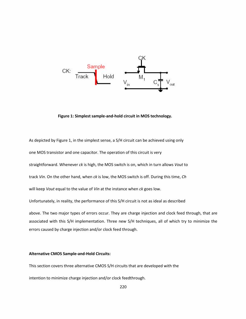
220
Figure 1: Simplest sample-and-hold circuit in MOS technology.
As depicted by Figure 1, in the simplest sense, a S/H circuit can be achieved using only
one MOS transistor and one capacitor. The operation of this circuit is very
straightforward. Whenever ck is high, the MOS switch is on, which in turn allows Vout to
track Vin. On the other hand, when ck is low, the MOS switch is off. During this time, Ch
will keep Vout equal to the value of Vin at the instance when ck goes low.
Unfortunately, in reality, the performance of this S/H circuit is not as ideal as described
above. The two major types of errors occur. They are charge injection and clock feed through, that are
associated with this S/H implementation. Three new S/H techniques, all of which try to minimize the
errors caused by charge injection and/or clock feed through.
Alternative CMOS Sample-and-Hold Circuits:
This section covers three alternative CMOS S/H circuits that are developed with the
intention to minimize charge injection and/or clock feedthrough.

221
Series Sampling:
The S/H circuit of Figure 1 is classified as parallel sampling because the hold capacitor is
in parallel with the signal. In parallel sampling, the input and the output are dc-coupled.
On the other hand, the S/H circuit shown in Figure 2 is referred to as series sampling
because the hold capacitor is in series with the signal.
Figure 2: Series sampling.
When the circuit is in sample mode, both switches S2 and S3 are on, while S1 is off. Then,S2 is turned off
first, which means Vout is equal to VCC (or VDD for most circuits) and the voltage drop across Ch will be
VCC – Vin. Subsequently, S3 is turned off and S1 is turned on simultaneously. By grounding node X, Vout
is now equal to VCC – Vin, and the drop from VCC to VCC – Vin is equal to the instantaneous value of the
input.
As a result, this is actually an inverted S/H circuit, which requires inversion of the signal at a later stage.
Since the hold capacitor is in series with the signal, series sampling can isolate the common-mode levels
of the input and the output. This is one advantage of series sampling over parallel sampling. In addition,
unlike parallel sampling, which suffers from signal-dependent charge injection, series sampling does not
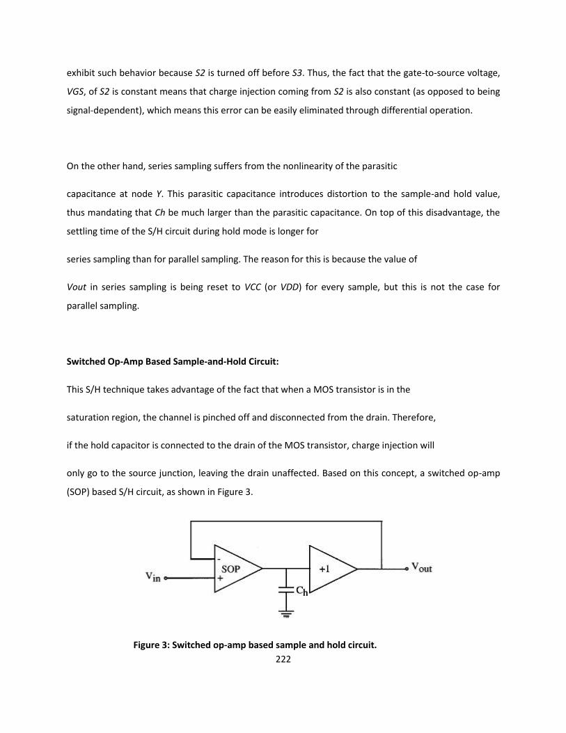
222
exhibit such behavior because S2 is turned off before S3. Thus, the fact that the gate-to-source voltage,
VGS, of S2 is constant means that charge injection coming from S2 is also constant (as opposed to being
signal-dependent), which means this error can be easily eliminated through differential operation.
On the other hand, series sampling suffers from the nonlinearity of the parasitic
capacitance at node Y. This parasitic capacitance introduces distortion to the sample-and hold value,
thus mandating that Ch be much larger than the parasitic capacitance. On top of this disadvantage, the
settling time of the S/H circuit during hold mode is longer for
series sampling than for parallel sampling. The reason for this is because the value of
Vout in series sampling is being reset to VCC (or VDD) for every sample, but this is not the case for
parallel sampling.
Switched Op-Amp Based Sample-and-Hold Circuit:
This S/H technique takes advantage of the fact that when a MOS transistor is in the
saturation region, the channel is pinched off and disconnected from the drain. Therefore,
if the hold capacitor is connected to the drain of the MOS transistor, charge injection will
only go to the source junction, leaving the drain unaffected. Based on this concept, a switched op-amp
(SOP) based S/H circuit, as shown in Figure 3.
Figure 3: Switched op-amp based sample and hold circuit.

223
During sample mode, the SOP behaves just like a regular op-amp, in which the value of
the output follows the value of the input. During hold mode, the MOS transistors at the
output node of the SOP are turned off while they are still operating in saturation, thus
preventing any channel charge from flowing into the output of the SOP. In addition, the
SOP is shut off and its output is held at high impedance, allowing the charge on Ch to be
preserved throughout the hold mode. On the other hand, the output buffer of this S/H
circuit is always operational during sample and hold mode and is always providing the
voltage on Ch to the output of the S/H circuit.
With the increasing demand for high-resolution and high-speed in date acquisition
systems, the performance of the S/H circuits is becoming more and more important.
This is especially true in ADCs since the performance of S/H circuits greatly affects the
speed and accuracy of ADCs. The fastest S/H circuits operate in open loop, but when
such circuits are implemented in CMOS technology, their accuracy is low. S/H circuits
that operate in closed loop configuration can achieve high resolution, but their
requirements for high gain circuit block, such as an op-amp, limits the speed of the
circuits. As a result, better and faster S/H circuits must be developed.
At the same time, the employment of low-voltage in VLSI technology requires that the
analog circuits be low-voltage as well. As a result of this, new researches in analog

224
circuits are now shifted from voltage-mode to current-mode. The advantages of current mode circuits
include low-voltage, low-power, and high-speed. Therefore, future
researches of S/H circuit should also shift toward current-mode S/H techniques.
The above figure shows a sample and hold circuit with MOSFET as Switch acting as a sampling device
and also consists of a holding capacitor Cs to store the sample values until the next sample comes in.
This is a high speed circuit as it is apparent that CMOS switch has a very negligible propagation delay.
Sample-and-hold (S/H) is an important analog building block that has many applications. The simplest
S/H circuit can be constructed using only one MOS transistor and one hold capacitor. However, due to
the limitations of the MOS transistor switches, errors due to charge injection and clock feed through
restrict the performance of S/H circuits. As a result, different S/H techniques and architectures are
developed with the intention to reduce or eliminate these errors. Three of these alternative S/H circuits:
series sampling, SOP based S/H circuit, and bottom plate S/H circuit with bootstrapped switch, more

225
new S/H techniques and architectures need to be proposed in order to meet the increasing demand for
high-speed, low-power, and low voltage S/H circuits for data acquisition systems.
LF 398 IC- Functional Diagram
Connection Diagram
A TO D CONVERTER- SPECIFICATIONS
Like DAC, ADCs are also having many important specifications. Some of them are Resolution,
Quantization error, Conversion time, Analog error, Linearity error, DNL error, INL error & Input voltage
range.
Resolution:

226
The resolution refers to the finest minimum change in the signal which is accepted for conversion, and it
is decided with respect to number of bits. It is given as 1/2n, where ‘n’ is the number of bits in the digital
output word. As it is clear, that the resolution can be improved by increasing the number of bits or the
number of bits representing the given analog input voltage.
Resolution can also be defined as the ratio of change in the value of input voltage Vi, needed to change
the digital output by 1 LSB. It is given as
Resolution = ViFS / (2n – 1)
Where ‘ViFS’ is the full-scale input voltage.
‘n’ is the number of output bits.
Quantization error:
If the binary output bit combination is such that for all the values of input voltage Vi between any two
voltage levels, there is a unavoidable uncertainty about the exact value of Vi when the output is a
particular binary combination. This uncertainty is termed as quantization error. Its value is ± (1/2) LSB.
And it is given as,
QE = ViFS / 2(2n – 1)
Where ‘ViFS’ is the full-scale input voltage
‘n’ is the number of output bits.
Maximum the number of bits selected, finer the resolution and smaller the quantization error.
Conversion Time:

227
It is defined as the total time required for an A/D converter to convert an analog signal to digital output.
It depends on the conversion technique and propagation delay of the circuit components.
Analog error:
An error occurring due to the variations in DC switching point of the comparator, resistors, reference
voltage source, ripples and noises introduced by the circuit components is termed as Analog error.
Linearity Error:
It is defined as the measure of variation in voltage step size. It indicates the difference between the
transitions for a minimum step of input voltage change. This is normally specified as fraction of LSB.
DNL (Differential Non-Linearity) Error:
The analog input levels that trigger any two successive output codes should differ by 1 LSB. Any
deviation from this 1 LSB value is called as DNL error.
INL (Integral Non-Linearity Error:
The deviation of characteristics of an ADC due to missing codes causes INL error. The maximum
deviation of the code from its ideal value after nulling the offset and gain errors is called as Integral Non-
Linearity Error.
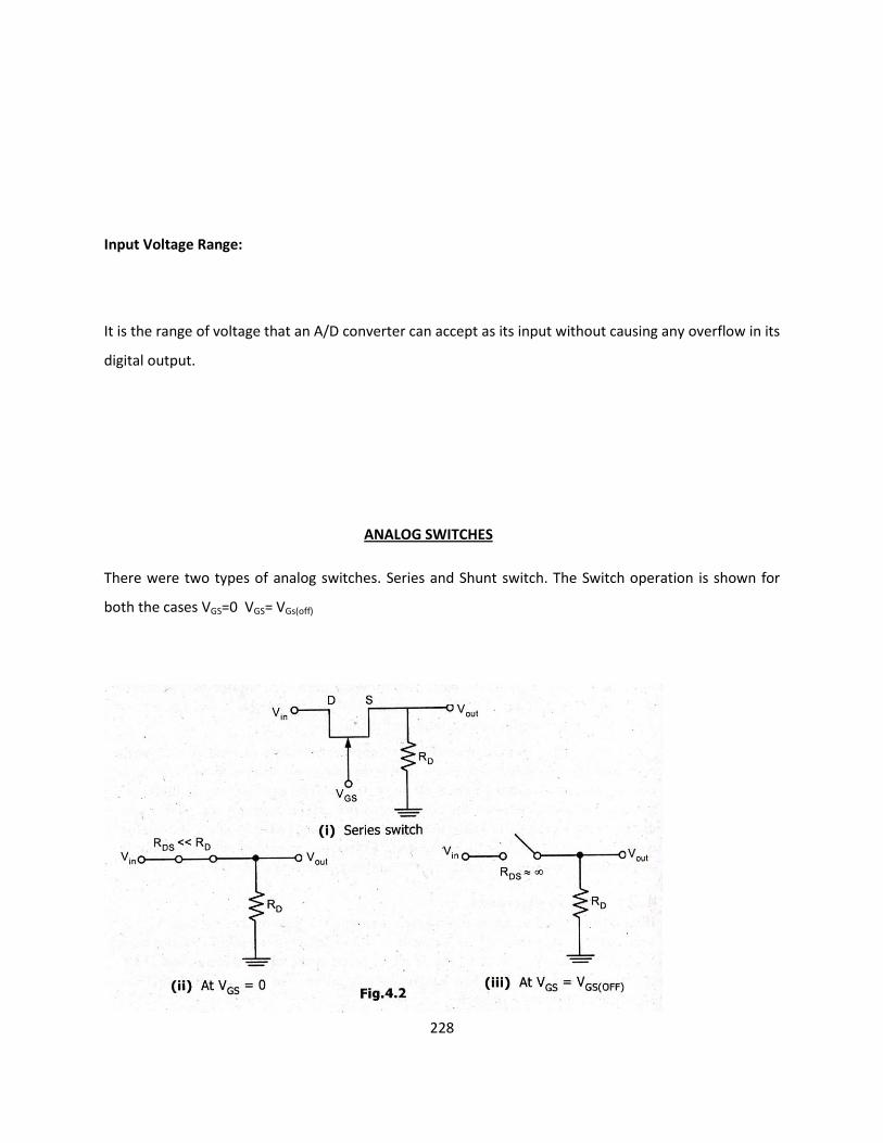
228
Input Voltage Range:
It is the range of voltage that an A/D converter can accept as its input without causing any overflow in its
digital output.
ANALOG SWITCHES
There were two types of analog switches. Series and Shunt switch. The Switch operation is shown for
both the cases VGS=0 VGS= VGs(off)
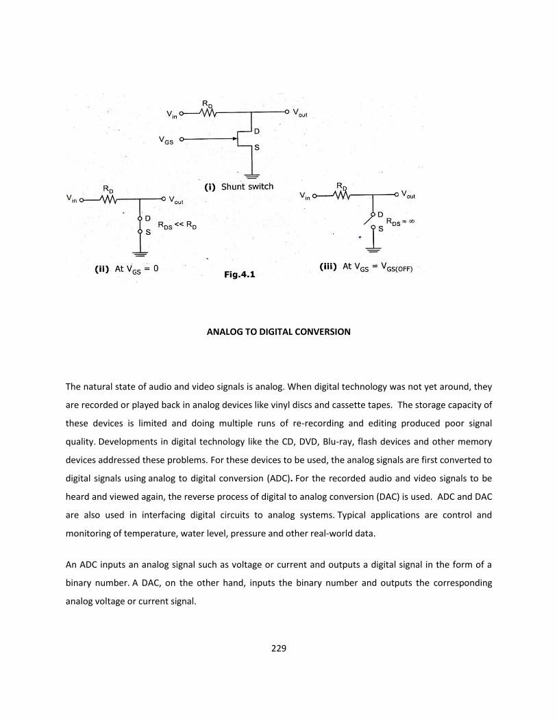
229
ANALOG TO DIGITAL CONVERSION
The natural state of audio and video signals is analog. When digital technology was not yet around, they
are recorded or played back in analog devices like vinyl discs and cassette tapes. The storage capacity of
these devices is limited and doing multiple runs of re-recording and editing produced poor signal
quality. Developments in digital technology like the CD, DVD, Blu-ray, flash devices and other memory
devices addressed these problems. For these devices to be used, the analog signals are first converted to
digital signals using analog to digital conversion (ADC). For the recorded audio and video signals to be
heard and viewed again, the reverse process of digital to analog conversion (DAC) is used. ADC and DAC
are also used in interfacing digital circuits to analog systems. Typical applications are control and
monitoring of temperature, water level, pressure and other real-world data.
An ADC inputs an analog signal such as voltage or current and outputs a digital signal in the form of a
binary number. A DAC, on the other hand, inputs the binary number and outputs the corresponding
analog voltage or current signal.

230
Sampling rate
The analog signal is continuous in time and it is necessary to convert this to a flow of digital values. It is
therefore required to define the rate at which new digital values are sampled from the analog signal.
The rate of new values is called the sampling rate or sampling frequency of the converter.
A continuously varying band limited signal can be sampled (that is, the signal values at intervals of time
T, the sampling time, are measured and stored) and then the original signal can be exactly reproduced
from the discrete-time values by an interpolation formula. The accuracy is limited by quantization error.
However, this faithful reproduction is only possible if the sampling rate is higher than twice the highest
frequency of the signal. This is essentially what is embodied in the Shannon-Nyquist sampling theorem.
Since a practical ADC cannot make an instantaneous conversion, the input value must necessarily be
held constant during the time that the converter performs a conversion (called theconversion time). An
input circuit called a sample and hold performs this task—in most cases by using a capacitor to store the
analog voltage at the input, and using an electronic switch or gate to disconnect the capacitor from the
input. Many ADC integrated circuits include the sample and hold subsystem internally.
Accuracy
An ADC has several sources of errors. Quantization error and (assuming the ADC is intended to
be linear) non-linearity is intrinsic to any analog-to-digital conversion. There is also a so-
called aperture error which is due to a clock jitter and is revealed when digitizing a time-variant
signal (not a constant value).

231
These errors are measured in a unit called the LSB, which is an abbreviation for least significant
bit. In the above example of an eight-bit ADC, an error of one LSB is 1/256 of the full signal
range, or about 0.4%.
Quantization error
Quantization error is due to the finite resolution of the ADC, and is an unavoidable imperfection
in all types of ADC. The magnitude of the quantization error at the sampling instant is between
zero and half of one LSB.
In the general case, the original signal is much larger than one LSB. When this happens,
the quantization error is not correlated with the signal, and has a uniform distribution. Its RMS
value is the standard deviation of this distribution, given by . In the eight-bit
ADC example, this represents 0.113% of the full signal range.
At lower levels the quantizing error becomes dependent of the input signal, resulting in
distortion. This distortion is created after the anti-aliasing filter, and if these distortions are above
1/2 the sample rate they will alias back into the audio band. In order to make the quantizing error
independent of the input signal, noise with amplitude of 1 quantization step is added to the
signal. This slightly reduces signal to noise ratio, but completely eliminates the distortion. It is
known as dither.
Non-linearity
All ADCs suffer from non-linearity errors caused by their physical imperfections, resulting in
their output to deviate from a linear function (or some other function, in the case of a deliberately
non-linear ADC) of their input. These errors can sometimes be mitigated by calibration, or
prevented by testing.
Important parameters for linearity are integral non-linearity (INL) and differential non-
linearity (DNL). These non-linearities reduce the dynamic range of the signals that can be
digitized by the ADC, also reducing the effective resolution of the ADC.

232
Types of ADC
Direct-conversion ADC/Flash type ADC:
This process is extremely fast with a sampling rate of up to 1 GHz. The resolution is however, limited
because of the large number of comparators and reference voltages required. The input signal is fed
simultaneously to all comparators. A priority encoder then generates a digital output that corresponds
with the highest activated comparator.

233
Successive-approximationADCs
Successive-approximation ADC is a conversion technique based on a successive-approximation register
(SAR). This is also called bit-weighing conversion that employs a comparator to weigh the applied input
voltage against the output of an N-bit digital-to-analog converter (DAC). The final result is obtained as a
sum of N weighting steps, in which each step is a single-bit conversion using the DAC output as a
reference. SAR converters sample at rates up to 1Mbps, requires a low supply current, and the cheapest
in terms of production cost.
A successive-approximation ADC uses a comparator to reject ranges of voltages, eventually settling on a
final voltage range. Successive approximation works by constantly comparing the input voltage to the
output of an internal digital to analog converter (DAC, fed by the current value of the approximation)
until the best approximation is achieved. At each step in this process, a binary value of the
approximation is stored in a successive approximation register (SAR). The SAR uses a reference voltage
(which is the largest signal the ADC is to convert) for comparisons. For example if the input voltage is 60
V and the reference voltage is 100 V, in the 1st clock cycle, 60 V is compared to 50 V (the reference,
divided by two. This is the voltage at the output of the internal DAC when the input is a '1' followed by
zeros), and the voltage from the comparator is positive (or '1') (because 60 V is greater than 50 V). At
this point the first binary digit (MSB) is set to a '1'. In the 2nd clock cycle the input voltage is compared
to 75 V (being halfway between 100 and 50 V: This is the output of the internal DAC when its input is
'11' followed by zeros) because 60 V is less than 75 V, the comparator output is now negative (or '0').
The second binary digit is therefore set to a '0'. In the 3rd clock cycle, the input voltage is compared with
62.5 V (halfway between 50 V and 75 V: This is the output of the internal DAC when its input is '101'
followed by zeros). The output of the comparator is negative or '0' (because 60 V is less than 62.5 V) so
the third binary digit is set to a 0. The fourth clock cycle similarly results in the fourth digit being a '1' (60
V is greater than 56.25 V, the DAC output for '1001' followed by zeros). The result of this would be in the
binary form 1001. This is also called bit-weighting conversion, and is similar to a binary. The analogue
value is rounded to the nearest binary value below, meaning this converter type is mid-rise (see above).
Because the approximations are successive (not simultaneous), the conversion takes one clock-cycle for
each bit of resolution desired. The clock frequency must be equal to the sampling frequency multiplied
by the number of bits of resolution desired. For example, to sample audio at 44.1 kHz with 32 bit

234
resolution, a clock frequency of over 1.4 MHz would be required. ADCs of this type have good
resolutions and quite wide ranges. They are more complex than some other designs.
IntegratingADCs
In an integrating ADC, a current, proportional to the input voltage, charges a capacitor for a fixed time
interval T charge. At the end of this interval, the device resets its counter and applies an opposite-
polarity negative reference voltage to the integrator input. Because of this, the capacitor is discharged
by a constant current until the integrator output voltage zero again. The T discharge interval is
proportional to the input voltage level and the resultant final count provides the digital output,
corresponding to the input signal. This type of ADCs is extremely slow devices with low input
bandwidths. Their advantage, however, is their ability to reject high-frequency noise and AC line noise
such as 50Hz or 60Hz. This makes them useful in noisy industrial environments and typical application is
in multi-meters.
An integrating ADC (also dual-slope or multi-slope ADC) applies the unknown input voltage to the input
of an integrator and allows the voltage to ramp for a fixed time period (the run-up period). Then a
known reference voltage of opposite polarity is applied to the integrator and is allowed to ramp until
the integrator output returns to zero (the run-down period). The input voltage is computed as a function
of the reference voltage, the constant run-up time period, and the measured run-down time period. The
run-down time measurement is usually made in units of the converter's clock, so longer integration
times allow for higher resolutions. Likewise, the speed of the converter can be improved by sacrificing

235
resolution. Converters of this type (or variations on the concept) are used in most digital voltmeters for
their linearity and flexibility.
Sigma-delta ADCs/ Over sampling Converters:
It consist of 2 main parts - modulator and digital filter. The modulator includes an integrator and a
comparator with a feedback loop that contains a 1-bit DAC. The modulator oversamples the input signal,
converting it to a serial bit stream with a frequency much higher than the required sampling rate. This is
then transform by the output filter to a sequence of parallel digital words at the sampling rate. The
characteristics of sigma-delta converters are high resolution, high accuracy, low noise and low cost.
Typical applications are for speech and audio.

236
A Sigma-Delta ADC (also known as a Delta-Sigma ADC) oversamples the desired signal by a large factor
and filters the desired signal band. Generally a smaller number of bits than required are converted using
a Flash ADC after the Filter. The resulting signal, along with the error generated by the discrete levels of
the Flash, is fed back and subtracted from the input to the filter. This negative feedback has the effect
of noise shaping the error due to the Flash so that it does not appear in the desired signal frequencies. A
digital filter (decimation filter) follows the ADC which reduces the sampling rate, filters off unwanted
noise signal and increases the resolution of the output. (sigma-delta modulation, also called delta-sigma
modulation)
A/D Using Voltage to time conversion:
The Block diagram shows the basic voltage to time conversion type of A to D converter. Here the cycles
of variable frequency source are counted for a fixed period. It is possible to make an A/D converter by
counting the cycles of a fixed-frequency source for a variable period. For this, the analog voltage
required to be converted to a proportional time period.
As shown in the diagram, A negative reference voltage -VR is applied to an integrator, whose output is
connected to the inverting input of the comparator. The output of the comparator is at 1 as long as the
output of the integrator Vo is less than Va. At t = T, Vc goes low and switch S remains open. When VEN
goes high, the switch S is closed, thereby discharging the capacitor. Also the NAND gate is disabled. The
waveforms are shown here.

237
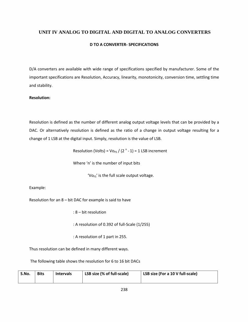
238
UNIT IV ANALOG TO DIGITAL AND DIGITAL TO ANALOG CONVERTERS
D TO A CONVERTER- SPECIFICATIONS
D/A converters are available with wide range of specifications specified by manufacturer. Some of the
important specifications are Resolution, Accuracy, linearity, monotonicity, conversion time, settling time
and stability.
Resolution:
Resolution is defined as the number of different analog output voltage levels that can be provided by a
DAC. Or alternatively resolution is defined as the ratio of a change in output voltage resulting for a
change of 1 LSB at the digital input. Simply, resolution is the value of LSB.
Resolution (Volts) = VoFS / (2 n - 1) = 1 LSB increment
Where ‘n’ is the number of input bits
‘VoFS’ is the full scale output voltage.
Example:
Resolution for an 8 – bit DAC for example is said to have
: 8 – bit resolution
: A resolution of 0.392 of full-Scale (1/255)
: A resolution of 1 part in 255.
Thus resolution can be defined in many different ways.
The following table shows the resolution for 6 to 16 bit DACs
S.No. Bits Intervals LSB size (% of full-scale) LSB size (For a 10 V full-scale)

239
1. 6 63 1.588 158.8 mV
2. 8 255 0.392 39.2 mV
3. 10 1023 0.0978 9.78 mV
4. 12 4095 0.0244 2.44 mV
5. 14 16383 0.0061 0.61 mV
6. 16 65535 0.0015 0.15 mV
Accuracy:
Absolute accuracy is the maximum deviation between the actual converter output and the ideal
converter output. The ideal converter is the one which does not suffer from any problem. Whereas, the
actual converter output deviates due to the drift in component values, mismatches, aging, noise and
other sources of errors.
The relative accuracy is the maximum deviation after the gain and offset errors have been removed.
Accuracy is also given in terms of LSB increments or percentage of full-scale voltage. Normally, the data
sheet of a D/A converter specifies the relative accuracy rather than absolute accuracy.
Linearity:
Linearity error is the maximum deviation in step size from the ideal step size. Some D/A converters are
having a linearity error as low as 0.001% of full scale. The linearity of a D/A converter is defined as the
precision or exactness with which the digital input is converted into analog output. An ideal D/A

240
converter produces equal increments or step sizes at output for every change in equal increments of
binary input.
Monotonicity:
A Digital to Analog converter is said to be monotonic if the analog output increases for an increase in the
digital input. A monotonic characteristics is essential in control applications. Otherwise it would lead to
oscillations. If a DAC has to be monotonic, the error should be less than ± (1/2) LSB at each output level.
Hence all the D/A converters are designed such that the linearity error satisfies the above condition.
When a D/A Converter doesn’t satisfy the condition described above, then, the output voltage may
decrease for an increase in the binary input.
Conversion Time:
It is the time taken for the D/A converter to produce the analog output for the given binary input signal.
It depends on the response time of switches and the output of the
Amplifier. D/A converters speed can be defined by this parameter. It is also called as setting time.
Settling time:
It is one of the important dynamic parameter. It represents the time it takes for the output to settle
within a specified band ± (1/2) LSB of its final value following a code change at the input (Usually a full-
scale change). It depends on the switching time of the logic circuitry due to internal parasitic

241
capacitances and inductances. A typical settling time ranges from 100 ns to 10 µs depending on the
word length and type of circuit used.
Stability:
The ability of a DAC to produce a stable output all the time is called as Stability. The performance of a
converter changes with drift in temperature, aging and power supply variations. So all the parameters
such as offset, gain, linearity error & monotonicity may change from the values specified in the
datasheet. Temperature sensitivity defines the stability of a D/A converter.
DIGITAL TO ANALOG CONVERSION
A DAC converts an abstract finite-precision number (usually a fixed-point binary number) into
a concrete physical quantity (e.g., a voltage or a pressure). In particular, DACs are often used to
convert finite-precision time series data to a continually-varying physical signal.
A typical DAC converts the abstract numbers into a concrete sequence of impulses that are then
processed by a reconstruction filter using some form of interpolation to fill in data between the
impulses. Other DAC methods (e.g., methods based on Delta-sigma modulation) produce
a pulse-density modulated signal that can then be filtered in a similar way to produce a smoothly-
varying signal.
By the Nyquist–Shannon sampling theorem, sampled data can be reconstructed perfectly
provided that its bandwidth meets certain requirements (e.g., a baseband signal
with bandwidth less than the Nyquist frequency). However, even with an ideal reconstruction
filter, digital sampling introduces quantization that makes perfect reconstruction practically
impossible. Increasing the digital resolution (i.e., increasing the number of bits used in each
sample) or introducing sampling dither can reduce this error.
DACs are at the beginning of the analog signal chain, which makes them very important to system
performance. The most important characteristics of these devices are:

242
Resolution: This is the number of possible output levels the DAC is designed to reproduce. This is usually
stated as the number of bits it uses, which is the base two logarithm of the number of levels. For
instance a 1 bit DAC is designed to reproduce 2 (21) levels while an 8 bit DAC is designed for 256 (28)
levels. Resolution is related to the effective number of bits(ENOB) which is a measurement of the actual
resolution attained by the DAC.
Maximum sampling frequency: This is a measurement of the maximum speed at which the DACs
circuitry can operate and still produce the correct output. As stated in the Nyquist–Shannon sampling
theorem, a signal must be sampled at over twice the frequency of the desired signal. For instance, to
reproduce signals in all the audible spectrum, which includes frequencies of up to 20 kHz, it is necessary
to use DACs that operate at over 40 kHz. The CD standard samples audio at 44.1 kHz, thus DACs of this
frequency are often used. A common frequency in cheap computer sound cards is 48 kHz—many work
at only this frequency, offering the use of other sample rates only through (often poor)
internal resampling.
Monotonicity: This refers to the ability of a DAC's analog output to move only in the direction that the
digital input moves (i.e., if the input increases, the output doesn't dip before asserting the correct
output.) This characteristic is very important for DACs used as a low frequency signal source or as a
digitally programmable trim element.
THD+N: This is a measurement of the distortion and noise introduced to the signal by the DAC. It is
expressed as a percentage of the total power of unwanted harmonic distortion and noise that
accompany the desired signal. This is a very important DAC characteristic for dynamic and small signal
DAC applications.
Dynamic range: This is a measurement of the difference between the largest and smallest signals the
DAC can reproduce expressed in decibels. This is usually related to DAC resolution and noise floor.
Other measurements, such as phase distortion and sampling period instability, can also be very
important for some applications.
BINARY-WEIGHTED RESISTOR DAC

243
The binary-weighted-resistor DAC employs the characteristics of the inverting summer Op Amp circuit.
In this type of DAC, the output voltage is the inverted sum of all the input voltages. If the input resistor
values are set to multiples of two: 1R, 2R and 4R, the output voltage would be equal to the sum of V1,
V2/2 and V3/4. V1 corresponds to the most significant bit (MSB) while V3 corresponds to the least
significant bit (LSB).
The circuit for a 4-bit DAC using binary weighted resistor network is shown below:
The binary inputs, ai (where i = 1, 2, 3 and 4) have values of either 0 or 1. The value, 0, represents an
open switch while 1 represents a closed switch.

244
The operational amplifier is used as a summing amplifier, which gives a weighted sum of the binary
input based on the voltage, Vref.
For a 4-bit DAC, the relationship between Vout and the binary input is as follows:
The negative sign associated with the analog output is due to the connection to a summing amplifier,
which is a polarity-inverting amplifier. When a signal is applied to the latter type of amplifier, the
polarity of the signal is reversed (i.e. a + input becomes -, or vice versa).
For a n-bit DAC, the relationship between Vout and the binary input is as follows:
Analog Voltage Output: An Example
As an example, consider the following given parameters: Vref = 5 V, R = 0.5 k and Rf = 1 k. The voltage
outputs, Vout, corresponding to the respective binary inputs are as follows:
Digital Input VOUT (Volts)

245
a1 a2 a3 a4
0 0 0 0 0
0 0 0 1 - 0.625
0 0 1 0 - 1.250
0 0 1 1 - 1.875
0 1 0 0 - 2.500
0 1 0 1 - 3.125
0 1 1 0 - 3.750
0 1 1 1 - 4.375
1 0 0 0 - 5.000
1 0 0 1 - 5.625
1 0 1 0 - 6.250
1 0 1 1 - 6.875
1 1 0 0 - 7.500
1 1 0 1 - 8.125
1 1 1 0 - 8.750

246
1 1 1 1 - 9.375
Table 1: Voltage Output of 4-bit DAC using Binary Weighted Resistor Network
The LSB, which is also the incremental step, has a value of - 0.625 V while the MSB or the full scale has a
value of - 9.375 V.
Practical Limitations:
o The most significant problem is the large difference in resistor values required between
the LSB and MSB, especially in the case of high resolution DACs (i.e. those that has large number
of bits). For example, in the case of a 12-bit DAC, if the MSB LSBis a staggering 2
o The maintanence of accurate resistances over a large range of values is problematic. With the
current IC fabrication technology, it is difficult to manufacture resistors over a wide resistance
range that maintain an accurate ratio especially with variations in temperature.
R-2R LADDER DAC
An enhancement of the binary-weighted resistor DAC is the R-2R ladder network. This type of DAC
utilizes Thevenin’s theorem in arriving at the desired output voltages. The R-2R network consists of
resistors with only two values - R and 2xR. If each input is supplied either 0 volts or reference
voltage, the output voltage will be an analog equivalent of the binary value of the three bits. VS2
corresponds to the most significant bit (MSB) while VS0 corresponds to the least significant bit (LSB).

247
Vout = - (VMSB + Vn + VLSB) = - (VRef + VRef/2 + VRef/ 4)
The R/2R DAC
An alternative to the binary-weighted-input DAC is the so-called R/2R DAC, which uses fewer
unique resistor values. A disadvantage of the former DAC design was its requirement of several
different precise input resistor values: one unique value per binary input bit. Manufacture may be
simplified if there are fewer different resistor values to purchase, stock, and sort prior to
assembly.
Of course, we could take our last DAC circuit and modify it to use a single input resistance
value, by connecting multiple resistors together in series:

248
Unfortunately, this approach merely substitutes one type of complexity for another: volume of
components over diversity of component values. There is, however, a more efficient design
methodology. By constructing a different kind of resistor network on the input of our summing
circuit, we can achieve the same kind of binary weighting with only two kinds of resistor values,
and with only a modest increase in resistor count. This "ladder" network looks like this:
Mathematically analyzing this ladder network is a bit more complex than for the previous circuit,
where each input resistor provided an easily-calculated gain for that bit. For those who are
interested in pursuing the intricacies of this circuit further, you may opt to use Thevenin's
theorem for each binary input (remember to consider the effects of the virtual ground), and/or

249
use a simulation program like SPICE to determine circuit response. Either way, you should
obtain the following table of figures:
---------------------------------
| Binary | Output voltage |
---------------------------------
| 000 | 0.00 V |
---------------------------------
| 001 | -1.25 V |
---------------------------------
| 010 | -2.50 V |
---------------------------------
| 011 | -3.75 V |
---------------------------------
| 100 | -5.00 V |
---------------------------------
| 101 | -6.25 V |
---------------------------------
| 110 | -7.50 V |
---------------------------------
| 111 | -8.75 V |
---------------------------------
As was the case with the binary-weighted DAC design, we can modify the value of the feedback
resistor to obtain any "span" desired. For example, if we're using +5 volts for a "high" voltage
level and 0 volts for a "low" voltage level, we can obtain an analog output directly corresponding
to the binary input (011 = -3 volts, 101 = -5 volts, 111 = -7 volts, etc.) by using a feedback
resistance with a value of 1.6R instead of 2R.

250
UNIT V WAVEFORM GENERATORS AND SPECIAL FUNCTION ICS
IC voltage regulators – LM317 – 723 regulators – Switching regulator – MA 7840 – LM 380
power amplifier – ICL 8038 function generator IC – Isolation amplifiers – Opto coupler – Opto
electronic ICs.
SAW-TOOTH WAVE GENERATOR
Circuit Diagram:
Output Waveform:
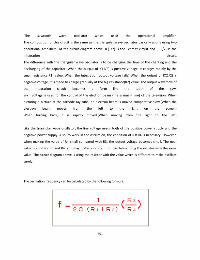
251
The sawtooth wave oscillator which used the operational amplifier.
The composition of this circuit is the same as the triangular wave oscillator basically and is using two
operational amplifiers. At the circuit diagram above, IC(1/2) is the Schmitt circuit and IC(2/2) is the
integration circuit.
The difference with the triangular wave oscillator is to be changing the time of the charging and the
discharging of the capacitor. When the output of IC(1/2) is positive voltage, it charges rapidly by the
small resistance(R1) value.(When the integration output voltage falls) When the output of IC(1/2) is
negative voltage, it is made to charge gradually at the big resistance(R2) value. The output waveform of
the integration circuit becomes a form like the tooth of the saw.
Such voltage is used for the control of the electron beam (the scanning line) of the television, When
picturing a picture at the cathode-ray tube, an electron beam is moved comparative slow.(When the
electron beam moves from the left to the right on the screen)
When turning back, it is rapidly moved.(When moving from the right to the left)
Like the triangular wave oscillator, the line voltage needs both of the positive power supply and the
negative power supply. Also, to work in the oscillation, the condition of R3>R4 is necessary. However,
when making the value of R4 small compared with R3, the output voltage becomes small. The near
value is good for R3 and R4. You may make opposite if not oscillating using the resistor with the same
value. The circuit diagram above is using the resistor with the value which is different to make oscillate
surely.
The oscillation frequency can be calculated by the following formula.
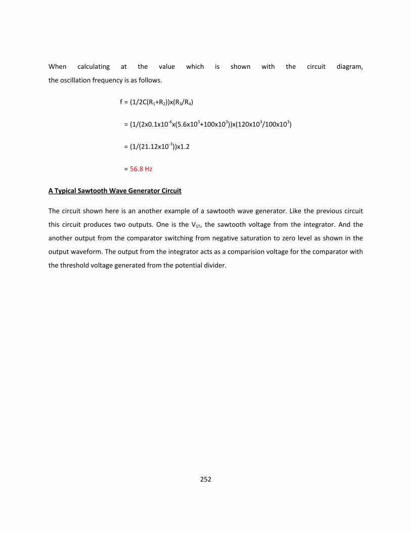
252
When calculating at the value which is shown with the circuit diagram,
the oscillation frequency is as follows.
f = (1/2C(R1+R2))x(R3/R4)
= (1/(2x0.1x10-6x(5.6x103+100x103))x(120x103/100x103)
= (1/(21.12x10-3))x1.2
= 56.8 Hz
A Typical Sawtooth Wave Generator Circuit
The circuit shown here is an another example of a sawtooth wave generator. Like the previous circuit
this circuit produces two outputs. One is the VST, the sawtooth voltage from the integrator. And the
another output from the comparator switching from negative saturation to zero level as shown in the
output waveform. The output from the integrator acts as a comparision voltage for the comparator with
the threshold voltage generated from the potential divider.
253
OUPUT WAVEFORM
FUNCTION GENERATOR IC 8038:

254
Fig: Functional block diagram of Function generator
Output Waveform:
255
It consists of two current sources, two comparators, two buffers, one FF and a sine wave converter.
Pin description:
Pin 1 & Pin 12: Sine wave adjusts:
The distortion in the sine wave output can be reduced by adjusting the 100KΩ pots connected
between pin12 & pin11 and between pin 1 & 6.
Pin 2 Sine Wave Output:
Sine wave output is available at this pin. The amplitude of this sine wave is 0.22 Vcc.
Where ± 5V ≤ Vcc ≤ ± 15 V.
Pin 3 Triangular Wave output:
Triangular wave is available at this pin. The amplitude of the triangular wave is 0.33Vcc. Where ±
5V ≤ Vcc ≤ ± 15 V.
Pin 4 & Pin 5 Duty cycle / Frequency adjust:
The symmetry of all the output wave forms & 50% duty cycle for the square wave output is
adjusted by the external resistors connected from Vcc to pin 4. These external resistors & capacitors at
pin 10 will decide the frequency of the output wave forms.

256
Pin 6 + Vcc:
Positive supply voltage the value of which is between 10 & 30V is applied to this pin.
Pin 7 : FM Bias:
This pin along with pin no8 is used to TEST the IC 8038.
Pin9 : Square Wave Output:
A square wave output is available at this pin. It is an open collector output so that this pin can be
connected through the load to different power supply voltages. This arrangement is very useful in
making the square wave output.
Pin 10 : Timing Capacitors:
The external capacitor C connected to this pin will decide the output frequency along with the
resistors connected to pin 4 & 5.
Pin 11 : -VEE or Ground:
If a single polarity supply is to be used then this pin is connected to supply ground & if (±) supply
voltages are to be used then (-) supply is connected to this pin.
Pin 13 & Pin 14: NC (No Connection)
Important features of IC 8038:

257
1. All the outputs are simultaneously available.
2. Frequency range : 0.001Hz to 500kHz
3. Low distortion in the output wave forms.
4. Low frequency drift due to change in temperature.
5. Easy to use.
Parameters:
(i) Frequency of the output wave form:
The output frequency dependent on the values of resistors R1 & R2 along with the external
capacitor C connected at pin 10.
If RA= RB = R & if RC is adjusted for 50% duty cycle then
fo = RC
3.0 ; RA = R1, RB = R3, RC = R2
(ii) Duty cycle / Frequency Adjust : (Pin 4 & 5):
Duty cycle as well as the frequency of the output wave form can be adjusted by controlling the values of
external resistors at pin 4 & 5.
The values of resistors RA & RB connected between Vcc * pin 4 & 5 respectively along with the
capacitor connected at pin 10 decide the frequency of the wave form.
The values of RA & RB should be in the range of 1kΩ to 1MΩ.
(iii) FM Bias:
The FM Bias input (pin7) corresponds to the junction of resistors R1 & R2.
The voltage Vin is the voltage between Vcc & pin8 and it decides the output frequency.

258
The output frequency is proportional to Vin as given by the following expression
For RA = RB (50% duty cycle).
fo = CRAVcc
Vin5.1 ; where C is the timing capacitor
With pin 7 & 8 connected to each other the output frequency is given by
fo = RC
3.0
where R = RA = RB for 50% duty cycle.
This is because Vin = 21
1
RR
R Vcc
(iv) FM Sweep input (pin 8):
This input should be connected to pin 7, if we want a constant output frequency.
But if the output frequency is supposed to vary, then a variable dc voltage should be applied
to this pin.
The voltage between Vcc & pin 8 is called Vin and it decides the output frequency as,
1.5 Vin
fo = ---------------
C RA Vcc
A potentiometer can be connected to this pin to obtain the required variable voltage required to change
the output frequency.

259
THE 555 TIMER IC
The 555 is a monolithic timing circuit that can produce accurate & highly stable time delays or
oscillation. The timer basically operates in one of two modes: either
(i) Monostable (one - shot) multivibrator or
(ii) Astable (free running) multivibrator
The important features of the 555 timer are these:
(i) It operates on +5v to +18 v supply voltages
(ii) It has an adjustable duty cycle
(iii) Timing is from microseconds to hours
(iv) It has a current o/p
PIN CONFIGURATION OF 555 TIMER:
Pin description:
Pin 1: Ground:

260
All voltages are measured with respect to this terminal.
Pin 2: Trigger:
The o/p of the timer depends on the amplitude of the external trigger pulse applied to this pin.
Pin 3: Output:
There are 2 ways a load can be connected to the o/p terminal either between pin3 & ground or
between pin 3 & supply voltage
(Between Pin 3 & Ground ON load )
(Between Pin 3 & + Vcc OFF load )
(i) When the input is low:
The load current flows through the load connected between Pin 3 & +Vcc in to the
output terminal & is called the sink current.
(ii) When the output is high:
The current through the load connected between Pin 3 & +Vcc (i.e. ON load) is zero.
However the output terminal supplies current to the normally OFF load. This current is
called the source current.
Pin 4: Reset:
The 555 timer can be reset (disabled) by applying a negative pulse to this pin. When the reset
function is not in use, the reset terminal should be connected to +Vcc to avoid any false triggering.
Pin 5: Control voltage:
An external voltage applied to this terminal changes the threshold as well as trigger voltage. In
other words by connecting a potentiometer between this pin & GND, the pulse width of the output
waveform can be varied. When not used, the control pin should be bypassed to ground with 0.01
capacitor to prevent any noise problems.

261
Pin 6: Threshold:
This is the non inverting input terminal of upper comparator which monitors the voltage across
the external capacitor.
Pin 7: Discharge:
This pin is connected internally to the collector of transistor Q1.
When the output is high Q1 is OFF.
When the output is low Q is (saturated) ON.
Pin 8: +Vcc:
The supply voltage of +5V to +18V is applied to this pin with respect to ground.
Block Diagram of 555 Timer IC:

262
From the above figure, three 5k internal resistors act as voltage divider providing bias voltage of 2/3 Vcc
to the upper comparator & 1/3 Vcc to the lower comparator. It is possible to vary time electronically by
applying a modulation voltage to the control voltage input terminal (5).
(i) In the Stable state:
The output of the control FF is high. This means that the output is low because of power
amplifier which is basically an inverter. Q = 1; Output = 0
(ii) At the Negative going trigger pulse:
The trigger passes through (Vcc/3) the output of the lower comparator goes high & sets the FF.
Q = 1; Q = 0

263
(iii) At the Positive going trigger pulse: It passes through 2/3Vcc, the output of the upper comparator
goes high and resets the FF. Q = 0; Q = 1
The reset input (pin 4) provides a mechanism to reset the FF in a manner which overrides the effect of
any instruction coming to FF from lower comparator.
Monostable Operation:
Fig : 555 connected as a Monostable Multivibrator
Model Graph:

264
Initially when the output is low, i.e. the circuit is in a stable state, transistor Q1 is ON & capacitor C is
shorted to ground. The output remains low. During negative going trigger pulse, transistor Q1 is OFF,
which releases the short circuit across the external capacitor C & drives the output high. Now the
capacitor C starts charging toward Vcc through RA. When the voltage across the capacitor equals 2/3
Vcc, upper comparator switches from low to high. i.e. Q = 0, the transistor Q1 = OFF ; the output is
high.
(a)

265
(b)
(c)
(d)
(e)
Since C is unclamped, voltage across it rises exponentially through R towards Vcc with a time constant
RC (fig b) as shown in below. After the time period, the upper comparator resets the FF, i.e. Q = 1, Q1 =
ON; the output is low.[i.e discharging the capacitor C to ground potential (fig c)].
The voltage across the capacitor as in fig (b) is given by

266
Vc = Vcc (1-e-t/RC) ……………. (1)
Therefore At t = T, Vc = 2/3 Vcc
2/3 Vcc = Vcc(1-e-T/RC)
or
T = RC ln (1/3)
Or
T = 1.1RC seconds ……………. (2)
If the reset is applied Q2 = OFF, Q1 = ON, timing capacitor C immediately discharged. The output now
will be as in figure (d & e). If the reset is released output will still remain low until a negative going
trigger pulse is again applied at pin 2.
Applications of Monostable Mode of Operation:
(a) Frequency Divider:
The 555 timer as a monostable mode. It can be used as a frequency divider by adjusting the
length of the timing cycle tp with respect to the time period T of the trigger input. To use the monostable
multivibrator as a divide by 2 circuit, the timing interval tp must be a larger than the time period of the
trigger input. [Divide by 2 tp > T of the trigger]
By the same concept, to use the monostable multivibrator as a divide by 3 circuit, tp must be
slightly larger than twice the period of the input trigger signal & so on, [ divide by 3 tp > 2T of trigger]

267
(b) Pulse width modulation:
Fig: Pulse Width Modulation
268
Output Waveform
Pulse width of a carrier wave changes in accordance with the value of a incoming (modulating
signal) is known as PWM. It is basically monostable multivibrator. A modulating signal is fed in to the
control voltage (pin 5). Internally, the control voltage is adjusted to 2/3 Vcc externally applied
modulating signal changes the control voltage level of upper comparator. As a result, the required to
change the capacitor up to threshold voltage level changes, giving PWM output.
(c) Pulse Stretcher:
This application makes use of the fact that the output pulse width (timing interval) of the
monostable multivibrator is of longer duration than the negative pulse width of the input trigger. As
such, the output pulse width of the monostable multivibrator can be viewed as a stretched version of
the narrow input pulse, hence the name “ Pulse stretcher”. Often, narrow –pulse width signals are not
suitable for driving an LED display, mainly because of their very narrow pulse widths. In other words, the
LED may be flashing but not be visible to the eye because its on time is infinitesimally small compared to
its off time. The 55 pulse stretcher can be used to remedy this problem. The LED will be ON during the
timing interval tp = 1.1RAC which can be varied by changing the value of RA & C.

269
Fig: Pulse Stretcher
The 555 timer as an Astable Multivibrator:
An Astable multivibrator, often called a free running multivibrator, is a rectangular wave
generating circuit. Unlike the monostable multivibrator, this circuit does not require an external trigger
to change the state of the output, hence the name free running. However, the time during which the
output is either high or low is determined by 2 resistors and capacitors, which are externally connected
to the 55 timer.
Fig: Astable Multivibrator

270
Model Graph
The above figures show the 555 timer connected as an astable multivibrator and its model graph
Initially, when the output is high :
Capacitor C starts charging toward Vcc through RA & RB. However, as soon as voltage across the
capacitor equals 2/3 Vcc. Upper comparator triggers the FF & output switches low.
When the output becomes Low:
Capacitor C starts discharging through RB and transistor Q1, when the voltage across C equals 1/3 Vcc,
lower comparator output triggers the FF & the output goes High. Then cycle repeats. The capacitor is
periodically charged & discharged between 2/3 Vcc & 1/3 Vcc respectively. The time during which the
capacitor charges from 1/3 Vcc to 2/3 Vcc equal to the time the output is high & is given by

271
tc = (RA+RB)C ln 2……………(1) Where [ln 2 = 0.69]
= 0.69 (RA+RB)C
Where RA & RB are in ohms. And C is in farads.
Similarly, the time during which the capacitors discharges from 2/3 Vcc to 1/3 Vcc is equal to the time,
the output is low and is given by,
tc = RB C ln 2
td = 0.69 RB C …………………..(2)
where RB is in ohms and C is in farads.
Thus the total period of the output waveform is
T = tc + td = 0.69 (RA+2RB)C …………….(3)
This, in turn, gives the frequency of oscillation as,f 0 = 1/T = 1.45/(RA+2RB)C ………(4)
Equation 4 indicates that the frequency f 0 is independent of the supply voltage Vcc. Often the term duty
cycle is used in conjunction with the astable multivibrator. The duty cycle is the ratio of the time tc
during which the output is high to the total time period T. It is generally expressed as a percentage.
% duty cycle = (tc / T )* 100
% DC = [(RA+RB)/ /(RA+2RB)] * 100

272
Astable Multivibrator Applications:
(a) Square wave oscillator:
Fig: Square Wave Oscillator
With out reducing RA = 0 ohm, the astable multivibrator can be used to produce square wave
output. Simply by connecting diode D across Resistor RB. The capacitor C charges through RA & diode D
to approximately
2/3 Vcc & discharges through RB & Q1 until the capacitor voltage equals approximately 1/3 Vcc, then the
cycle repeats.
To obtain a square wave output, RA must be a combination of a fixed resistor & potentiometer so that
the potentiometer can be adjusted for the exact square wave.

273
(b) Free – running Ramp generator:
The astable multivibrator can be used as a free – running ramp generator when resistor RA & RB
are replaced by a current mirror.
The current mirror starts charging capacitor C toward Vcc at a constant rate.
When voltage across C equals to 2/3 Vcc, upper comparator turns transistor Q1 ON & C rapidly
discharges through transistor Q1.
When voltage across C equals to 1/3 Vcc, lower comparator switches transistor OFF & then
capacitor C starts charging up again..
Thus the charge – discharge cycle keeps repeating.
The discharging time of the capacitor is relatively negligible compared to its charging time.
The time period of the ramp waveform is equal to the charging time & is approximately is given
by,
T = VccC/3IC ………………………… (1)

274
IC = (Vcc - VBE)/R = constant current
Therefore the free – running frequency of ramp generator is
f 0 = 3IC/ Vcc C ……………………….(2)
SWITCHING REGULATORS
Introduction
The switching regulator is increasing in popularity because it offers the advantages of higher power
conversion efficiency and increased design flexibility (multiple output voltages of different polarities can
be generated from a single input voltage).
Although most power supplies used in amateur shacks are of the linear regulator type, an
increasing number of switching power supplies have become available to the amateur. For most
amateurs the switching regulator is still somewhat of a mystery. One might wonder why we even
bother with these power supplies, when the existing linear types work just fine. The primary
advantage of a switching regulator is very high efficiency, a lot less heat and smaller size. To
understand how these black boxes work lets take a look at a traditional linear regulator at right. As
we see in the diagram, the linear regulator is really nothing more than a variable resistor. The
resistance of the regulator varies in accordance with the load resulting in a constant output voltage

275
The primary filter capacitor is placed on the input to the regulator to help filter out the 60 cycle
ripple. The linear regulator does an excellent job but not without cost. For example, if the output
voltage is 12 volts and the input voltage is 24 volts then we must drop 12 volts across the regulator.
At output currents of 10 amps this translates into 120 watts (12 volts times 10 amps) of heat energy
that the regulator must dissipate. Is it any wonder why we have to use those massive heat sinks? As
we can see this results in a mere 50% efficiency for the linear regulator and a lot of wasted power
which is normally transformed into heat.
The time that the switch remains closed during each switch cycle is varied to maintain a constant
output voltage. Notice that the primary filter capacitor is on the output of the regulator and not

276
the input. As is apparent, the switching regulator is much more efficient than the linear regulator
achieving efficiencies as high as 80% to 95% in some circuits. The obvious result is smaller heat
sinks, less heat and smaller overall size of the power supply.
The previous diagram is really an over simplification of a switching regulator circuit. An actual
switching regulator circuit more closely resembles the circuit below: Now lets take a look at a very
basic switching regulator at right.
As we see can see, the switching regulator is really nothing more than just a simple switch. This
switch goes on and off at a fixed rate usually between 50Khz to 100Khz as set by the circuit.
As we see above the switching regulator appears to have a few more components than a linear
regulator. Diode D1 and Inductor L1 play a very specific role in this circuit and are found in almost
every switching regulator. First, diode D1 has to be a Schottky or other very fast switching diode. A
1N4001 just won't switch fast enough in this circuit. Inductor L1 must be a type of core that does
not saturate under high currents. Capacitor C1 is normally a low ESR (Equivalent Series Resistance)
type.
To understand the action of D1 and L1, lets look at what happens when S1 is closed as indicated
below:

277
As we see above, L1, which tends to oppose the rising current, begins to generate an
electromagnetic field in its core. Notice that diode D1 is reversed biased and is essentially an open
circuit at this point. Now lets take a look at what happens when S1 opens below:
As we see in this diagram the electromagnetic field that was built up in L1 is now discharging and
generating a current in the reverse polarity. As a result, D1 is now conducting and will continue
until the field in L1 is diminished. This action is similar to the charging and discharging of capacitor
C1. The use of this inductor/diode combination gives us even more efficiency and augments the
filtering of C1.
Because of the unique nature of switching regulators, very special design considerations are
required. Because the switching system operates in the 50 to 100 kHz region and has an almost
square waveform, it is rich in harmonics way up into the HF and even the VHF/UHF region. Special

278
filtering is required, along with shielding, minimized lead lengths and all sorts of toroidal filters on
leads going outside the case. The switching regulator also has a minimum load requirement, which
is determined by the inductor value. Without the minimum load, the regulator will generate
excessive noise and harmonics and could even damage itself. (This is why it is not a good idea to
turn on a computer switching power supply without some type of load connected.) To meet this
requirement, many designers use a cooling fan and or a minimum load which switches out when
no longer needed.
Fortunately, recent switching regulator IC's address most of these design problems quite well.
Because of lowered component costs as well as a better understanding of switching regulator
technology, we are starting to see even more switching power supplies replacing traditionally
linear only applications. It is no doubt that we will see fewer linear power supplies being used in
the future.
In this article we addressed basic switching regulator design concepts and it is hoped that amateurs
will begin to look at switching regulators much more seriously when they decide to replace an old
power supply. In a future construction article, we will review an actual switching regulator circuit.
IC VOLTAGE REGULATORS
Four most commonly used switching converter types:
Buck: used the reduce a DC voltage to a lower DC voltage.
Boost: provides an output voltage that is higher than the input.
Buck-Boost (invert): an output voltage is generated opposite in polarity to the input.
Flyback: an output voltage that is less than or greater than the input can be generated, as well as
multiple outputs.
Converters:
Push-Pull: A two-transistor converter that is especially efficient at low input voltages.
279
Half-Bridge: A two-transistor converter used in many off-line applications.
Full-Bridge: A four-transistor converter (usually used in off-line designs) that can
generate the highest output power of all the types listed.
Application information will be provided along with circuit examples that illustrate
some applications of Buck, Boost, and Flyback regulators.
Switching Fundamentals
The law of inductance
If a voltage is forced across an inductor, a current will flow through that inductor (and
this current will vary with time). The current flowing in an inductor will be time-varying even if the
forcing voltage is constant. It is equally correct to say that if a time-varying current is forced to flow in an
inductor, a voltage across the inductor will result. The fundamental law that defines the relationship
between the voltage and current in an inductor is given by the equation:
v = L (di/dt)
Two important characteristics of an inductor that follow directly from the law of
inductance are:
1) A voltage across an inductor results only from a current that changes with
time. A steady (DC) current flowing in an inductor causes no voltage across it
(except for the tiny voltage drop across the copper used in the windings).

280
2) A current flowing in an inductor can not change value instantly (in zero time), as this would require
infinite voltage to force it to happen. However, the faster the current is changed in an inductor, the
larger the resulting voltage will be. Note: Unlike the current flowing in the inductor, the voltage across it
can change instantly (in zero time). The principles of inductance are illustrated by the information
contained in Figure.
The important parameter is the di/dt term, which is simply a measure of how the
current changes with time. When the current is plotted versus time, the value of
di/dt is defined as the slope of the current plot at any given point. The graph on the left shows that
current which is constant with time has a di/dt value of zero, and results in no voltage across the
inductor. The center graph shows that a current which is increasing with time has a positive di/dt value,
resulting in a positive inductor voltage.
Current that decreases with time (shown in the right-hand graph) gives a negative
value for di/dt and inductor voltage. It is important to note that a linear current ramp in an inductor
(either up or down) occurs only when it has a constant voltage across it.
Transformer Operation:
A transformer is a device that has two or more magnetically-coupled windings. The
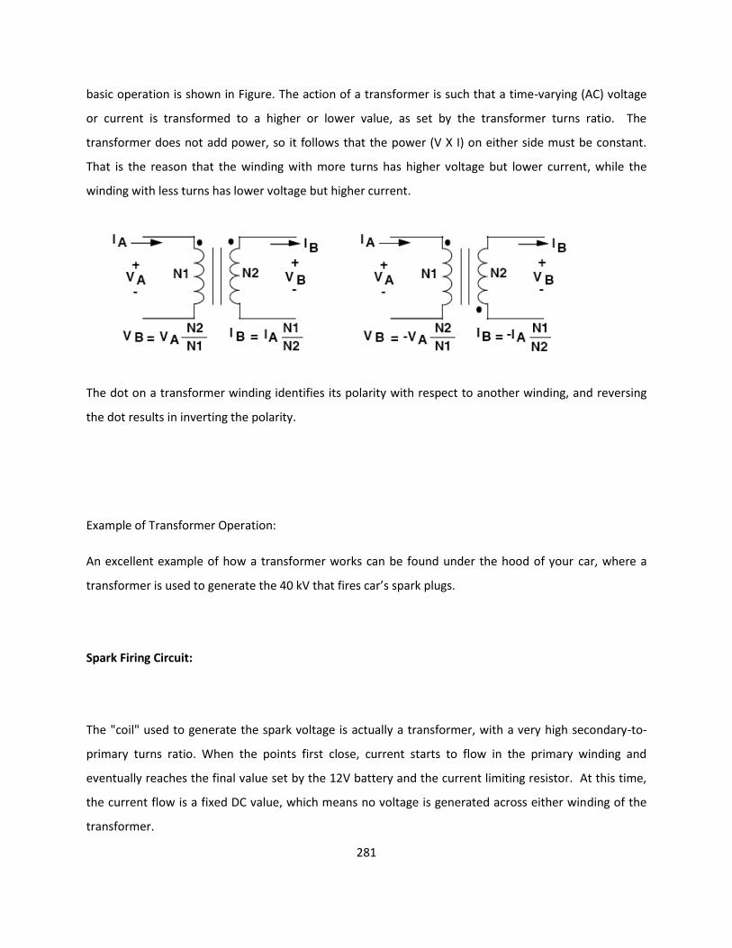
281
basic operation is shown in Figure. The action of a transformer is such that a time-varying (AC) voltage
or current is transformed to a higher or lower value, as set by the transformer turns ratio. The
transformer does not add power, so it follows that the power (V X I) on either side must be constant.
That is the reason that the winding with more turns has higher voltage but lower current, while the
winding with less turns has lower voltage but higher current.
The dot on a transformer winding identifies its polarity with respect to another winding, and reversing
the dot results in inverting the polarity.
Example of Transformer Operation:
An excellent example of how a transformer works can be found under the hood of your car, where a
transformer is used to generate the 40 kV that fires car’s spark plugs.
Spark Firing Circuit:
The "coil" used to generate the spark voltage is actually a transformer, with a very high secondary-to-
primary turns ratio. When the points first close, current starts to flow in the primary winding and
eventually reaches the final value set by the 12V battery and the current limiting resistor. At this time,
the current flow is a fixed DC value, which means no voltage is generated across either winding of the
transformer.

282
When the points open, the current in the primary winding collapses very quickly, causing a large voltage
to appear across this winding. This voltage on the primary is magnetically coupled to (and stepped up
by) the secondary winding, generating a voltage of 30 kV - 40 kV on the secondary side. As explained
previously, the law of inductance says that it is not possible to instantly break the current flowing in an
inductor (because an infinite voltage would be required to make it happen).
This principle is what causes the arcing across the contacts used in switches that are in circuits with
highly inductive loads. When the switch just begins to open, the high voltage generated allows
electrons to jump the air gap so that the current flow does not actually stop instantly. Placing a
capacitor across the contacts helps to reduce this arcing effect. In the automobile ignition, a capacitor is
placed across the points to minimize damage due to arcing when the points "break" the current flowing
in the low-voltage coil winding (in car manuals, this capacitor is referred to as a "condenser").
Pulse Width Modulation (PWM):
All of the switching converters that will be covered in this paper use a form of output voltage regulation
known as Pulse Width Modulation (PWM). Put simply, the feedback loop adjusts (corrects) the output
voltage by changing the ON time of the switching element in the converter. As an example of how PWM
works, we will examine the result of applying a series of square wave pulses to an L-C filter (see Figure).

283
The series of square wave pulses is filtered and provides a DC output voltage that is equal to the peak
pulse amplitude multiplied times the duty cycle (duty cycle is defined as the switch ON time divided by
the total period). This relationship explains how the output voltage can be directly controlled by
changing the ON time of the switch.
Switching Converter Topologies
The most commonly used DC-DC converter circuits will now be presented along with
the basic principles of operation.
Buck Regulator:
The most commonly used switching converter is the Buck, which is used to down-convert a DC voltage
to a lower DC voltage of the same polarity. This is essential in systems that use distributed power rails
(like 24V to 48V), which must be locally converted to 15V, 12V or 5V with very little power loss. The Buck
converter uses a transistor as a switch that alternately connects and disconnects the input voltage to an
inductor (see Figure).
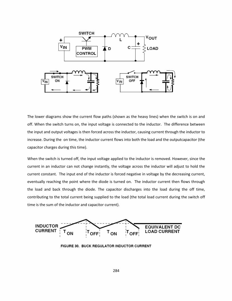
284
The lower diagrams show the current flow paths (shown as the heavy lines) when the switch is on and
off. When the switch turns on, the input voltage is connected to the inductor. The difference between
the input and output voltages is then forced across the inductor, causing current through the inductor to
increase. During the on time, the inductor current flows into both the load and the outputcapacitor (the
capacitor charges during this time).
When the switch is turned off, the input voltage applied to the inductor is removed. However, since the
current in an inductor can not change instantly, the voltage across the inductor will adjust to hold the
current constant. The input end of the inductor is forced negative in voltage by the decreasing current,
eventually reaching the point where the diode is turned on. The inductor current then flows through
the load and back through the diode. The capacitor discharges into the load during the off time,
contributing to the total current being supplied to the load (the total load current during the switch off
time is the sum of the inductor and capacitor current).

285
The shape of the current flowing in the inductor is similar to previous figure. As explained, the current
through the inductor ramps up when the switch is on, and ramps down when the switch is off. The DC
load current from the regulated output is the average value of the inductor current. The peak-to-peak
difference in the inductor current waveform is referred to as the inductor ripple current, and the
inductor is typically selected large enough to keep this ripple current less than 20% to 30% of the rated
DC current.
Continuous vs. Discontinuous operation
In most Buck regulator applications, the inductor current never drops to zero during
Full-load operation (this is defined as continuous mode operation). Overall performance is usually
better using continuous mode, and it allows maximum output power to be obtained from a given input
voltage and switch current rating. In applications where the maximum load current is fairly low, it can be
advantageous to design for discontinuous mode operation. In these cases, operating in discontinuous
mode can result in a smaller overall converter size (because a smaller inductor can be
used).Discontinuous mode operation at lower load current values is generally harmless, and even
converters designed for continuous mode operation at full load will become discontinuous as the load
current is decreased (usually causing no problems).
Boost Regulator:
The Boost regulator takes a DC input voltage and produces a DC output voltage that is higher in value
than the input (but of the same polarity). The Boost regulator is shown in Figure, along with details
showing the path of current flow during the switch on and off time. Whenever the switch is on, the
input voltage is forced across the inductor which causes the current through it to increase (ramp up).

286
When the switch is off, the decreasing inductor current forces the "switch" end of the inductor to swing
positive. This forward biases the diode, allowing the capacitor to charge up to a voltage that is higher
than the input voltage. During steady-state operation, the inductor current flows into both the output
capacitor and the load during the switch off time. When the switch is on, the load current is supplied
only by the capacitor.
Output Current and Load power:
An important design consideration in the Boost regulator is that the output load current and the switch
current are not equal, and the maximum available load current is always less than the current rating of
the switch transistor. It should be noted that the maximum total power available for conversion in any
regulator is equal to the input voltage multiplied times the maximum average input current (which is
less than the current rating of the switch transistor). Since the output voltage of the Boost is higher than
the input voltage, it follows that the output current must be lower than the input current.
Buck-Boost (Inverting) Regulator:

287
The Buck-Boost or Inverting regulator takes a DC input voltage and produces a DC output voltage that is
opposite in polarity to the input. The negative output voltage can be either larger or smaller in
magnitude than the input voltage. The Inverting regulator is shown in Figure.
When the switch is on, the input voltage is forced across the inductor, causing an increasing current flow
through it. During the on time, the discharge of the output capacitor is the only source of load current.
This requires that the charge lost from the output capacitor during the on time be replenished during
the off time. When the switch turns off, the decreasing current flow in the inductor causes the voltage
at the diode end to swing negative. This action turns on the diode, allowing the current in the inductor
to supply both the output capacitor and the load. As shown, the load current is supplied by inductor
when the switch is off, and by the output capacitor when the switch is on.
Flyback Regulator:
The Flyback is the most versatile of all the topologies, allowing the designer to create one or more
output voltages, some of which may be opposite in polarity. Flyback converters have gained popularity
in battery-powered systems, where a single voltage must be converted into the required system

288
voltages (for example, +5V, +12V and -12V) with very high power conversion efficiency. The basic single-
output flyback converter is shown in Figure.
The most important feature of the Flyback regulator is the transformer phasing, as shown by the dots on
the primary and secondary windings. When the switch is on, the input voltage is forced across the
transformer primary which causes an increasing flow of current through it. Note that the polarity of
the voltage on the primary is dot-negative (more negative at the dotted end), causing a voltage with the
same polarity to appear at the transformer secondary (the magnitude of the secondary voltage is set by
the transformer seconday-to-primary turns ratio).
The dot-negative voltage appearing across the secondary winding turns off the diode, reventing current
flow in the secondary winding during the switch on time. During this time, the load current must be
supplied by the output capacitor alone. When the switch turns off, the decreasing current flow in the
primary causes the voltage at the dot end to swing positive. At the same time, the primary voltage is
reflected to the secondary with the same polarity. The dot-positive voltage occurring across the
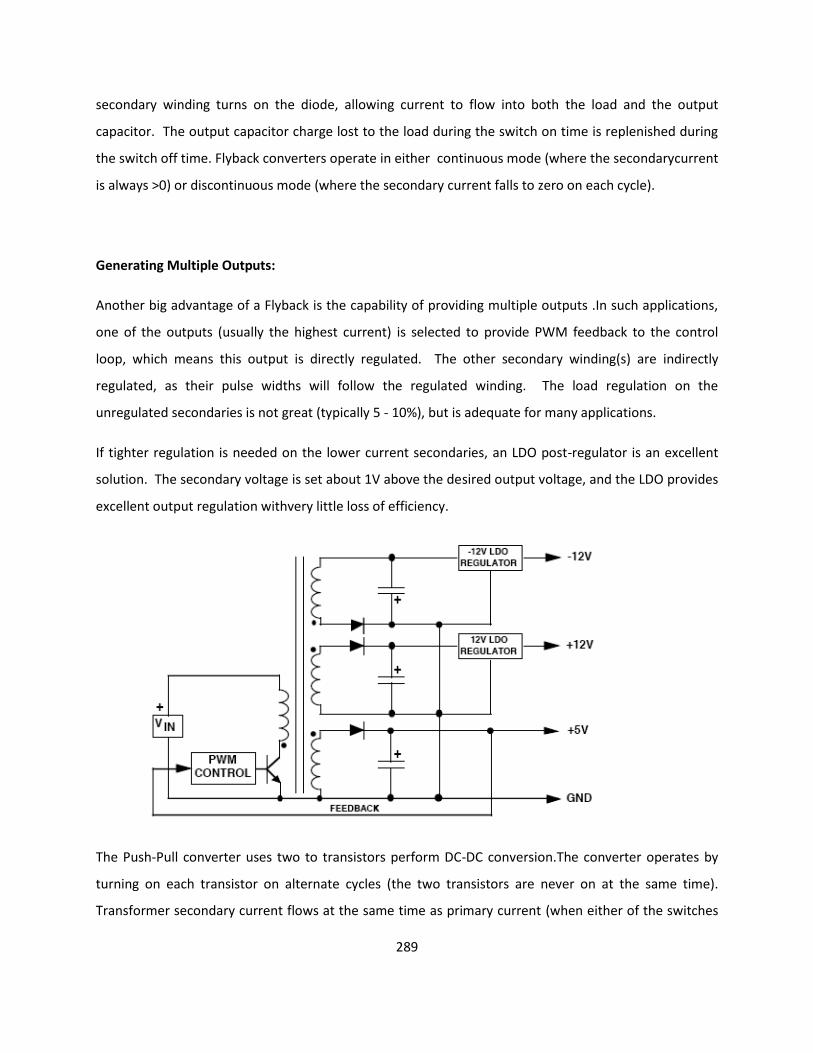
289
secondary winding turns on the diode, allowing current to flow into both the load and the output
capacitor. The output capacitor charge lost to the load during the switch on time is replenished during
the switch off time. Flyback converters operate in either continuous mode (where the secondarycurrent
is always >0) or discontinuous mode (where the secondary current falls to zero on each cycle).
Generating Multiple Outputs:
Another big advantage of a Flyback is the capability of providing multiple outputs .In such applications,
one of the outputs (usually the highest current) is selected to provide PWM feedback to the control
loop, which means this output is directly regulated. The other secondary winding(s) are indirectly
regulated, as their pulse widths will follow the regulated winding. The load regulation on the
unregulated secondaries is not great (typically 5 - 10%), but is adequate for many applications.
If tighter regulation is needed on the lower current secondaries, an LDO post-regulator is an excellent
solution. The secondary voltage is set about 1V above the desired output voltage, and the LDO provides
excellent output regulation withvery little loss of efficiency.
The Push-Pull converter uses two to transistors perform DC-DC conversion.The converter operates by
turning on each transistor on alternate cycles (the two transistors are never on at the same time).
Transformer secondary current flows at the same time as primary current (when either of the switches

290
is on). For example, when transistor "A" is turned on, the input voltage is forced across the upper
primary winding with dot-negative polarity. On the secondary side, a dot-negative voltage will appear
across the winding which turns on the bottom diode.This allows current to flow into the inductor to
supply both the output capacitor and the load. When transistor "B" is on, the input voltage is forced
across the lower primary winding with dot-positive polarity.
The same voltage polarity on the secondary turns on the top diode, and current flows into the output
capacitor and the load. An important characteristic of a Push-Pull converter is that the switch transistors
have to be able the stand off more than twice the input voltage: when one transistor is on (and the
input voltage is forced across one primary winding) the same magnitude voltage is induced across the
other primary winding, but it is "floating" on top of the input voltage. This puts the collector of the
turned-off transistor at twice the input voltage with respect to ground. The "double input voltage" rating
requirement of the switch transistors means the Push-Pull converter is best suited for lower input
voltage applications. It has been widely used in converters operating in 12V and 24V battery-powered
systems.

291
Figure shows a timing diagram which details the relationship of the input and output pulses. It is
important to note that frequency of the secondary side voltage pulses is twice the frequency of
operation of the PWM controller driving the two transistors. For example, if the PWM control chip was
set up to operate at 50 kHz on the primary
side, the frequency of the secondary pulses would be 100 kHz.
This highlights why the Push-Pull converter is well-suited for low voltage converters.
The voltage forced across each primary winding (which provides the power for conversion) is the full
input voltage minus only the saturation voltage of the switch. If MOS-FET power switches are used, the
voltage drop across the switches can be made extremely small, resulting in very high utilization of the
available input voltage. Another advantage of the Push-Pull converter is that it can also generate
multiple output voltages (by adding more secondary windings), some of which may be negative in
polarity. This allows a power supply operated from a single battery to provide all of the voltages
necessary for system operation.
A disadvantage of Push-Pull converters is that they require very good matching of

292
the switch transistors to prevent unequal on times, since this will result in saturation
of the transformer core (and failure of the converter).
Output Capacitor ESR effects:
The primary function of the output capacitor in a switching regulator is filtering. As the converter
operates, current must flow into and out of the output filter capacitor. The ESR of the output capacitor
directly affects the performance of the switching regulator. ESR is specified by the manufacturer on
good quality capacitors, but be certain that it is specified at the frequency of intended operation.
General-purpose electrolytes usually only specify ESR at 120 Hz, but capacitors intended for high-
frequency switching applications will have the ESR guaranteed at high frequency (like 20 kHz to 100
kHz). Some ESR dependent parameters are: Ripple Voltage: In most cases, the majority of the output
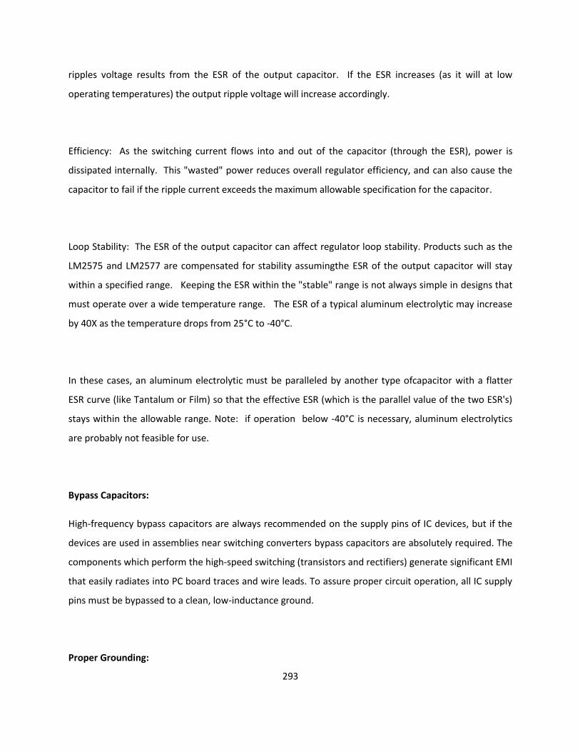
293
ripples voltage results from the ESR of the output capacitor. If the ESR increases (as it will at low
operating temperatures) the output ripple voltage will increase accordingly.
Efficiency: As the switching current flows into and out of the capacitor (through the ESR), power is
dissipated internally. This "wasted" power reduces overall regulator efficiency, and can also cause the
capacitor to fail if the ripple current exceeds the maximum allowable specification for the capacitor.
Loop Stability: The ESR of the output capacitor can affect regulator loop stability. Products such as the
LM2575 and LM2577 are compensated for stability assumingthe ESR of the output capacitor will stay
within a specified range. Keeping the ESR within the "stable" range is not always simple in designs that
must operate over a wide temperature range. The ESR of a typical aluminum electrolytic may increase
by 40X as the temperature drops from 25°C to -40°C.
In these cases, an aluminum electrolytic must be paralleled by another type ofcapacitor with a flatter
ESR curve (like Tantalum or Film) so that the effective ESR (which is the parallel value of the two ESR's)
stays within the allowable range. Note: if operation below -40°C is necessary, aluminum electrolytics
are probably not feasible for use.
Bypass Capacitors:
High-frequency bypass capacitors are always recommended on the supply pins of IC devices, but if the
devices are used in assemblies near switching converters bypass capacitors are absolutely required. The
components which perform the high-speed switching (transistors and rectifiers) generate significant EMI
that easily radiates into PC board traces and wire leads. To assure proper circuit operation, all IC supply
pins must be bypassed to a clean, low-inductance ground.
Proper Grounding:
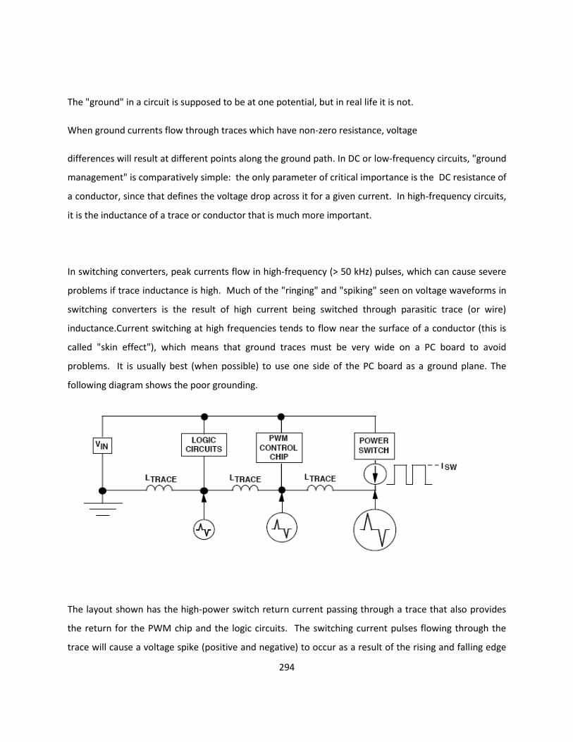
294
The "ground" in a circuit is supposed to be at one potential, but in real life it is not.
When ground currents flow through traces which have non-zero resistance, voltage
differences will result at different points along the ground path. In DC or low-frequency circuits, "ground
management" is comparatively simple: the only parameter of critical importance is the DC resistance of
a conductor, since that defines the voltage drop across it for a given current. In high-frequency circuits,
it is the inductance of a trace or conductor that is much more important.
In switching converters, peak currents flow in high-frequency (> 50 kHz) pulses, which can cause severe
problems if trace inductance is high. Much of the "ringing" and "spiking" seen on voltage waveforms in
switching converters is the result of high current being switched through parasitic trace (or wire)
inductance.Current switching at high frequencies tends to flow near the surface of a conductor (this is
called "skin effect"), which means that ground traces must be very wide on a PC board to avoid
problems. It is usually best (when possible) to use one side of the PC board as a ground plane. The
following diagram shows the poor grounding.
The layout shown has the high-power switch return current passing through a trace that also provides
the return for the PWM chip and the logic circuits. The switching current pulses flowing through the
trace will cause a voltage spike (positive and negative) to occur as a result of the rising and falling edge
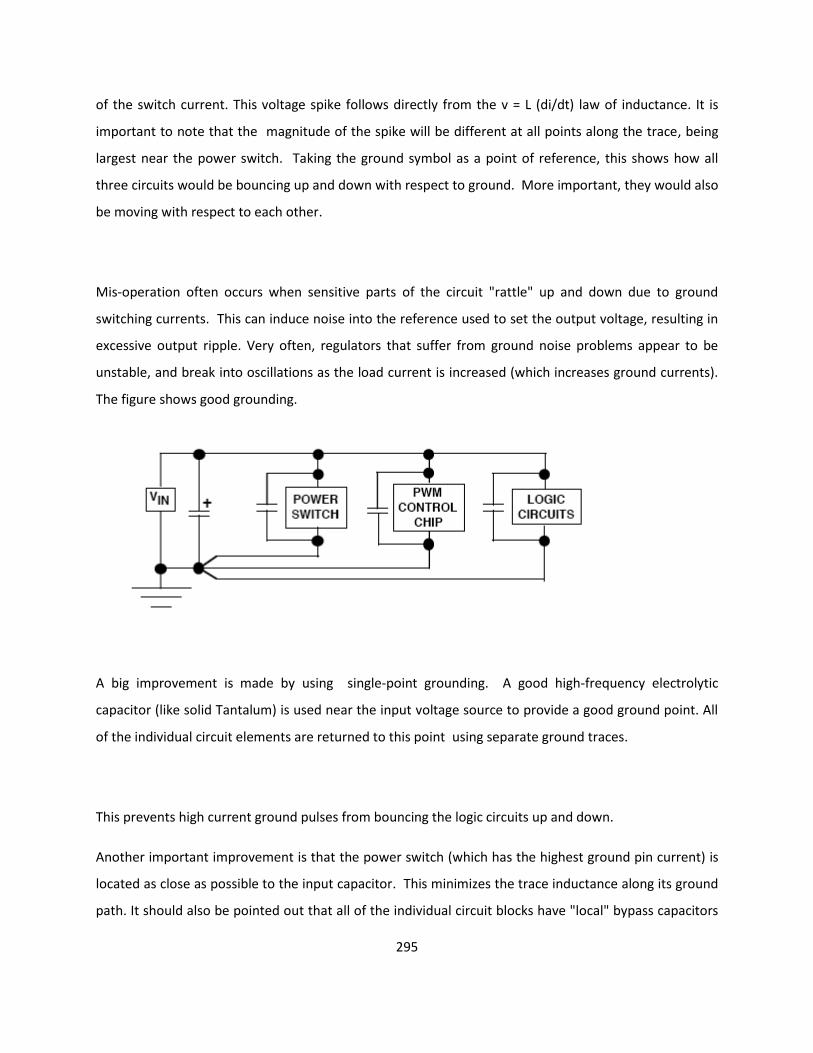
295
of the switch current. This voltage spike follows directly from the v = L (di/dt) law of inductance. It is
important to note that the magnitude of the spike will be different at all points along the trace, being
largest near the power switch. Taking the ground symbol as a point of reference, this shows how all
three circuits would be bouncing up and down with respect to ground. More important, they would also
be moving with respect to each other.
Mis-operation often occurs when sensitive parts of the circuit "rattle" up and down due to ground
switching currents. This can induce noise into the reference used to set the output voltage, resulting in
excessive output ripple. Very often, regulators that suffer from ground noise problems appear to be
unstable, and break into oscillations as the load current is increased (which increases ground currents).
The figure shows good grounding.
A big improvement is made by using single-point grounding. A good high-frequency electrolytic
capacitor (like solid Tantalum) is used near the input voltage source to provide a good ground point. All
of the individual circuit elements are returned to this point using separate ground traces.
This prevents high current ground pulses from bouncing the logic circuits up and down.
Another important improvement is that the power switch (which has the highest ground pin current) is
located as close as possible to the input capacitor. This minimizes the trace inductance along its ground
path. It should also be pointed out that all of the individual circuit blocks have "local" bypass capacitors

296
tied directly across them. The purpose of this capacitor is RF bypass, so it must be a ceramic or film
capacitor (or both).
A good value for bypassing logic devices would be 0.01 μF ceramic capacitor(s), distributed as required.
If the circuit to be bypassed generates large current pulses (like the power switch), more capacitance is
required. A good choice would be an aluminum electrolytic bypassed with a film and ceramic capacitor.
Exact size depends on peak current, but the more capacitance used, the better the result.
Transformer/Inductor Cores and Radiated Noise The type of core used in an inductor or transformer
directly affects its cost, size, and radiated noise characteristics. Electrical noise radiated by a
transformer is extremely important, as it may require shielding to prevent erratic operation of sensitive
circuits located near the switching regulator. The most commonly used core types will be presented,
listing the advantages and disadvantages of each.
Measuring Output Ripple Voltage:
The ripple appearing on the output of the switching regulator can be important to the circuits under
power. Getting an accurate measurement of the output ripple voltage is not always simple. If the
output voltage waveform is measured using an oscilloscope, an accurate result can only be obtained
using a differential measurement method. The differential measurement shown uses the second
channel of the oscilloscope to "cancel out" the signal that is common to both channels (by inverting the
B channel signal and adding it to the A channel).
The reason this method must be used is because the fast-switching components in a switching regulator
generate voltage spikes that have significant energy at very high frequencies. These signals can be
picked up very easily by "antennas" as small as the 3" ground lead on the scope probe. Assuming the
probes are reasonably well matched, the B channel probe will pick up the same radiated signal as the A
channel probe, which allows this "common-mode" signal to be eliminated by adding the inverted
channel B signal to channel A. It is often necessary to measure the RMS output ripple voltage, and this is

297
usually done with some type of digital voltmeter. If the reading obtained is to be meaningful, the
following must be considered:
Measuring Regulator Efficiency of DC-DC Converters:
The efficiency of a switching regulator is defined as:
PTOTAL
In determining converter efficiency, the first thing that must be measured is the total consumed power
(PTOTAL). Assuming a DC input voltage, PTOTAL is defined as the total power drawn from the source,
which is equal to:
PTOTAL = VIN X IIN (AVE)
It must be noted that the input current value used in the calculation must be the average value of the
waveform (the input current will not be DC or sinusoidal). Because the total power dissipated must be
constant from input to output, PTOTAL is also equal to the load power plus the internal regulator power
losses:
PTOTAL = PLOAD + PLOSSES
Measuring (or calculating) the power to the load is very simple, since the output voltage and current are
both DC. The load power is found by:
298
PLOAD = VOUT X ILOAD
Measuring the input power drawn from the source is not simple. Although the input voltage to the
regulator is DC, the current drawn at the input of a switching regulator is not. If a typical "clip-on"
current meter is used to measure the input current, the taken data will be essentially meaningless. The
average input current to the regulator can be measured with reasonable accuracy by using a wide-
bandwidth current probe connected to an oscilloscope.
The average value of input current can be closely estimated by drawing a horizontal
line that divides the waveform in such a way that the area of the figure above the
line will equal the "missing" area below the line. In this way, the "average" current shown is equivalent
to the value of DC current that would produce the same input power.
If more exact measurements are needed, it is possible to force the current in the line
going to the input of the DC-DC converter to be DC by using an L-C filter between
the power source and the input of the converter If the L-C filter components are adequate, the current
coming from the output of the DC power supply will be DC current (with no high-frequency switching
component) which means it can be accurately measured with a cheap clip-on ammeter and digital volt
meter.
It is essential that a large, low-ESR capacitor be placed at CIN to support the input
of the switching converter. The L-C filter that the converter sees looking back into
the source presents a high impedance for switching current, which means CIN is
necessary to provide the switching current required at the input of the converter.

299
Measuring Regulator Efficiency of Off-Line Converters:
Off-Line converters are powered directly from the AC line, by using a bridge rectifier
and capacitive filter to generate an unregulated DC voltage for conversion.
Measuring the total power drawn from the AC source is fairly difficult because of the
power factor. If both the voltage and current are sinusoidal, power factor is
defined as the cosine of the phase angle between the voltage and current
waveforms.
The capacitive-input filter in an off-line converter causes the input current to be very
non-sinusoidal. The current flows in narrow, high-amplitude pulses (called
Haversine pulses) which requires that the power factor be re-defined in such cases.
For capacitive-input filter converters, power factor is defined as:
P.F. = PREAL / PAPPARENT
LM 2577: An Example of a Complete FlyBack/ Boost Regulator IC
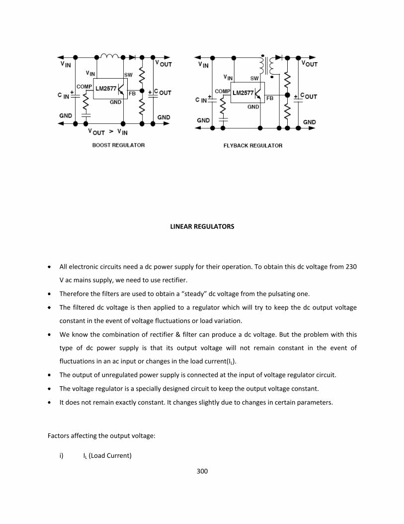
300
LINEAR REGULATORS
All electronic circuits need a dc power supply for their operation. To obtain this dc voltage from 230
V ac mains supply, we need to use rectifier.
Therefore the filters are used to obtain a “steady” dc voltage from the pulsating one.
The filtered dc voltage is then applied to a regulator which will try to keep the dc output voltage
constant in the event of voltage fluctuations or load variation.
We know the combination of rectifier & filter can produce a dc voltage. But the problem with this
type of dc power supply is that its output voltage will not remain constant in the event of
fluctuations in an ac input or changes in the load current(IL).
The output of unregulated power supply is connected at the input of voltage regulator circuit.
The voltage regulator is a specially designed circuit to keep the output voltage constant.
It does not remain exactly constant. It changes slightly due to changes in certain parameters.
Factors affecting the output voltage:
i) IL (Load Current)

301
ii) VIN (Input Voltage)
iii) T (Temperature)
IC Voltage Regulators:
They are basically series regulators with all the basic blocks present inside the IC. Therefore it is
easier to use IC voltage regulator instead of discrete voltage regulators.
Important features of IC Regulators:
1. Programmable output
2. Facility to boost the voltage/current
3. Internally provided short circuit current limiting
4. Thermal shutdown
5. Floating operation to facilitate higher voltage output
Classifications of IC voltage regulators:
IC Voltage Regulator
Fixed Volt Reg. Adjustable O/P Volt Reg Switching Reg
Positive/negative

302
Fixed & Adjustable output Voltage Regulators are known as Linear Regulator.
A series pass transistor is used and it operates always in its active region.
Switching Regulator:
1. Series Pass Transistor acts as a switch.
2. The amount of power dissipation in it decreases considerably.
3. Power saving result is higher efficiency compared to that of linear.
Adjustable Voltage Regulator:
Advantages of Adjustable Voltage Regulator over fixed voltage regulator are,
1. Adjustable output voltage from 1.2v to 57 v
2. Output current 0.10 to 1.5 A
3. Better load & line regulation
4. Improved overload protection
5. Improved reliability under the 100% thermal overloading
Adjustable Positive Voltage Regulator (LM317):
LM317 series adjustable 3 terminal positive voltage regulator, the three terminals are Vin, Vout &
adjustment (ADJ).

303
LM317 requires only 2 external resistors to set the output voltage.
LM317 produces a voltage of 1.25v between its output & adjustment terminals. This voltage is called
as Vref.
Vref (Reference Voltage) is a constant, hence current I1 flows through R1 will also be constant.
Because resistor R1 sets current I1. It is called “current set” or “program resistor”.
Resistor R2 is called as “Output set” resistors, hence current through this resistor is the sum of I1 &
Iadj
LM317 is designed in such as that Iadj is very small & constant with changes in line voltage & load
current.
The output voltage Vo is, Vo=R1I1+(I1+Iadj)R2 ------------- (1)
Where I1= Vref/R1
Vo =(Vref/R1)R1 + Vref/R1 + Iadj R2
= Vref + (Vref/R1)R2 + Iadj R2
Vo = Vref [1 + R2/R1] + Iadj R2 ------------- (2)
R1 = Current (I1) set resistor
R2 = output (Vo) set resistor
Vref = 1.25v which is a constant voltage between output and ADJ terminals.
Current Iadj is very small. Therefore the second term in (2) can be neglected.
Thus the final expression for the output voltage is given by
Vo= 1.25v[1 + R2/R1] -------------- (3)

304
Eqn (3) indicates that we can vary the output voltage by varying the resistance R2.
The value of R1 is normally kept constant at 240 ohms for all practical applications.
Practical Regulator using LM317:
If LM317 is far away from the input power supply, then 0.1μf disc type or 1μf tantalum capacitor
should be used at the input of LM317.
The output capacitor Co is optional. Co should be in the range of 1 to 1000μf.

305
The adjustment terminal is bypassed with a capacitor C2 this will improve the ripple rejection ratio
as high as 80 dB is obtainable at any output level.
When the filter capacitor is used, it is necessary to use the protective diodes.
These diodes do not allow the capacitor C2 to discharge through the low current point of the
regulator.
These diodes are required only for high output voltages (above 25v) & for higher values of output
capacitance 25μf and above.
IC 723 – GENERAL PURPOSE REGULATOR
Disadvantages of fixed voltage regulator:
1. Do not have the shot circuit protection
2. Output voltage is not adjustable
These limitations can be overcomes in IC723.
Features of IC723:
1. Unregulated dc supply voltage at the input between 9.5V & 40V
2. Adjustable regulated output voltage between 2 to 3V.
3. Maximum load current of 150 mA (ILmax = 150mA).
4. With the additional transistor used, ILmax upto 10A is obtainable.
5. Positive or Negative supply operation
6. Internal Power dissipation of 800mW.
7. Built in short circuit protection.
8. Very low temperature drift.
9. High ripple rejection.

306
The simplified functional block diagram can be divided in to 4 blocks.
1. Reference generating block
2. Error Amplifier
3. Series Pass transistor
4. Circuitry to limit the current
1. Reference Generating block:
The temperature compensated Zener diode, constant current source & voltage
reference amplifier together from the reference generating block. The Zener diode is used to
generate a fixed reference voltage internally. Constant current source will make the Zener diode
to operate at affixed point & it is applied to the Non – inverting terminal of error amplifier. The
Unregulated input voltage ±Vcc is applied to the voltage reference amplifier as well as error
amplifier.
2. Error Amplifier:
Error amplifier is a high gain differential amplifier with 2 input
(inverting & Non-inverting). The Non-inverting terminal is connected
to the internally generated reference voltage. The Inverting terminal is
connected to the full regulated output voltage.

307
Fig: Functional block diagram of IC723
Fig : Pin diagram of IC723
3. Series Pass Transistor:
Q1 is the internal series pass transistor which is driven by
the error amplifier. This transistor actually acts as a variable resistor
& regulates the output voltage. The collector of transistor Q1 is

308
connected to the Un-regulated power supply. The maximum collector
voltage of Q1 is limited to 36Volts. The maximum current which can
be supplied by Q1 is 150mA.
4. Circuitry to limit the current:
The internal transistor Q2 is used for current sensing & limiting. Q2 is normally
OFF transistor. It turns ON when the IL exceeds a predetermined limit.
Low voltage , Low current is capable of supplying load voltage which is equal to or between 2
to 7Volts.
Vload = 2 to 7V
Iload = 150mA

309
IC723 as a LOW voltage LOW current :
Typical circuit connection diagram
R1 & R2 from a potential divider between Vref & Gnd.
The Voltage across R2 is connected to the Non – inverting terminal of the regulator IC

310
Vnon-inv = 21
2
RR
R Vref
Gain of the internal error amplifier is large
Vnon-inv = Vin
Therefore the Vo is connected to the Inverting terminal through R3 & RSC must also be equal
to Vnon-inv
Vo = Vnon-inv = 21
2
RR
R Vref
R1 & R2 can be in the range of 1 KΩ to 10KΩ & value of R3 is given by
R3 = R1ll R2 = 2
21
RR
RR
Rsc (current sensing resistor) is connected between Cs & CL. The voltage drop across Rsc is
proportional to the IL.
This resistor supplies the output voltage in the range of 2 to 7 volts, but the load current can
be higher than 150mA.
The current sourcing capacity is increased by including a transistor Q in the circuit.
The output voltage , Vo = 21
2
RR
R Vref
IC723 as a HIGH voltage LOW Current:
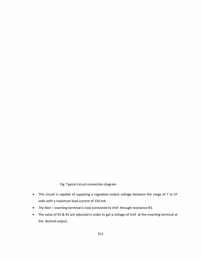
311
Fig: Typical circuit connection diagram
This circuit is capable of supplying a regulated output voltage between the range of 7 to 37
volts with a maximum load current of 150 mA.
The Non – inverting terminal is now connected to Vref through resistance R3.
The value of R1 & R2 are adjusted in order to get a voltage of Vref at the inverting terminal at
the desired output.
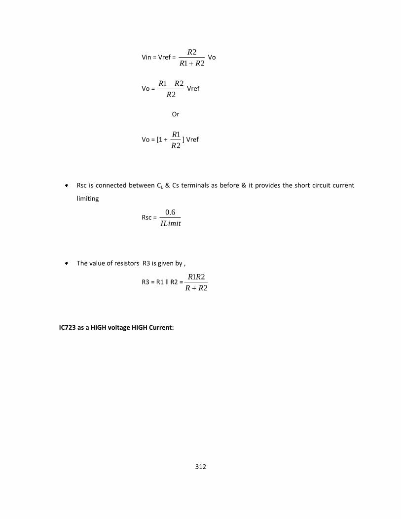
312
Vin = Vref = 21
2
RR
R Vo
Vo = 2
21
R
RR Vref
Or
Vo = [1 + 2
1
R
R] Vref
Rsc is connected between CL & Cs terminals as before & it provides the short circuit current
limiting
Rsc = ILimit
6.0
The value of resistors R3 is given by ,
R3 = R1 ll R2 =2
21
RR
RR
IC723 as a HIGH voltage HIGH Current:

313
An external transistor Q is added in the circuit for high voltage low current regulator to
improve its current sourcing capacity.
For this circuit the output voltage varies between 7 & 37V.
Transistor Q increase the current sourcing capacity thus IL(MAX) ia greater than 150mA.
The output voltage Vo is given by ,
R1+ R2
Vo= ------------ Vref
R2
The value of Rsc is given by Rsc = ILimit
6.0
SWITCHING REGULATOR:
An example of general purpose regulator is Motorola’s MC1723. It can be used in
many different ways, for example, as a fixed positive or negative output voltage regulator, variable
regulator or switching regulator because of its flexibility.
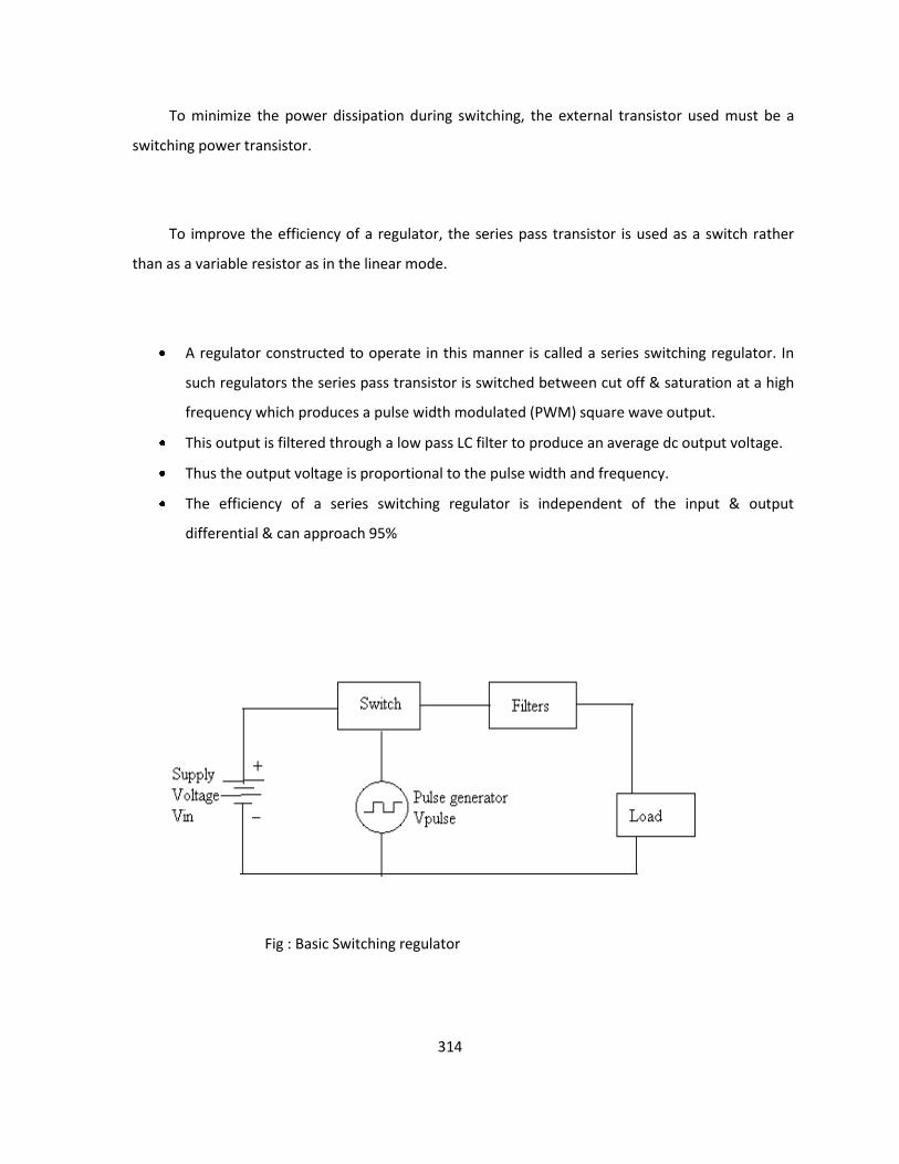
314
To minimize the power dissipation during switching, the external transistor used must be a
switching power transistor.
To improve the efficiency of a regulator, the series pass transistor is used as a switch rather
than as a variable resistor as in the linear mode.
A regulator constructed to operate in this manner is called a series switching regulator. In
such regulators the series pass transistor is switched between cut off & saturation at a high
frequency which produces a pulse width modulated (PWM) square wave output.
This output is filtered through a low pass LC filter to produce an average dc output voltage.
Thus the output voltage is proportional to the pulse width and frequency.
The efficiency of a series switching regulator is independent of the input & output
differential & can approach 95%
Fig : Basic Switching regulator

315
A basic switching regulator consists of 4 major components,
1. Voltage source Vin
2. Switch S1
3. Pulse generator Vpulse
4. Filter F1
1. Voltage Source Vin:
It may be any dc supply – a battery or an unregulated or a regulated voltage. The voltage source
must satisfy the following requirements.
It must supply the required output power & the losses associated with the switching
regulator.
It must be large enough to supply sufficient dynamic range for line & load regulations.
It must be sufficiently high to meet the minimum requirement of the regulator system to
be designed.
It may be required to store energy for a specified amount of time during power failures.
2. Switch S1:
It is typically a transistor or thyristor connected as a power switch & is operated in the saturated
mode. The pulse generator output alternately turns the switch ON & OFF
3. Pulse generator Vpulse:

316
It provides an asymmetrical square wave varying in either frequency or pulse width called
frequency modulation or pulse width modulation respectively. The most effective frequency range
for the pulse generator for optimum efficiency 20 KHz. This frequency is inaudible to the human
ear & also well within the switching speeds of most inexpensive transistors & diodes.
The duty cucly of the pulse wave form determines the relationship between the input &
output voltages. The duty cycle is the ratio of the on time ton, to the period T of the
pulse waveform.
Duty cycle = toffton
ton
= T
ton = ton f.
Where ton = On-time of the pulse waveform
toff=off-time of the pulse wave form
T = time period = ton + toff
= 1/frequency or
T = 1/f
Typical operating frequencies of switching regulator range from 10 to 50khz.

317
Lower operating frequency improve efficiency & reduce electrical noise, but require
large filter components (inductors & capacitors).
4. Filter F1:
It converts the pulse waveform from the output of the switch into a dc voltage. Since
this switching mechanism allows a conversion similar to transformers, the switching regulator is
often referred to as a dc transformer.
The output voltage Vo of the switching regulator is a function of duty cycle & the input
voltage Vin.
Vo is expressed as follows,
Vo = T
ton Vin
This equation indicates that, if time period T is constant, Vo is directly proportional to the
ON-time, ton for a given value of Vin. This method of changing the output voltage by
varying ton is referred to as a pulse width modulation.
Similarly, if ton is held constant, the output voltage Vo is inversely proportional to the
period T or directly proportional to the frequency of the pulse waveform. This method of
varying the output voltage is referred to as frequency modulation (FM).
Switching regulator can operate in any of 3 modes
i) Step – Down
ii) Step – Up
iii) Polarity inverting
MONOLITHIC SWITCHING REGULATOR [µA78S40]:

318
The µA78S40 consists of a temperature compensated voltage reference, duty cycle controllable
oscillator with an active current limit circuit, a high gain comparator, a high- current, high voltage output
switch, a power switching diode & an uncommitted op-amp.
Important features of the µA78S40 switching regulators are:
Step up, down & Inverting operation
Operation from 2.5 to 40V input
80dB line & load regulations
Output adjustable from 1.3 to 40V
Peak current to 1.5A without external resistors
Variable frequency, variable duty cycle device
The internal switching frequency is set by the timing capacitor CT, connected between pin12 & ground
pin 11. the initial duty cycle is 6:1. The switching frequency & duty cycle can be modified by the current
limit circuitry, IPKsense, pin14, 7 the comparator, pin9 & 10.
Comparator:
The comparator modifies the OFF time of the output switch transistor Q1 & Q2. In the step – up
& step down modes, the non-inverting input(pin9) of the comparator is connected to the voltage
reference of 1.3V (pin8) & the inverting input (pin10) is connected to the output terminal via the voltage
divider network.

319
Fig: Functional block diagram of µA78S40

320
In the Inverting mode the non – inverting input is connected to both the voltage reference
& the output terminal through 2 resistors & the inverting terminal is connected to ground.
When the output voltage is correct, the comparator output is in high state & has no effect on
the circuit operation.
However, if the output is too high & the voltage at the inverting terminal is higher than that at
the non-inverting terminal , then the comparator output goes low.
In the LOW state the comparator inhibits the turn on of the output switching transistors. This
means that, as long as the comparator output is low, the system is in off time.
As the output current rises or the output voltage falls, the off time of the system decreases.
Consequently, as the output current nears its maximum IoMAX, the off time approaches its
minimum value.
In all 3 modes (Step down, step up, Inverting), the current limit circuit is completed by connecting a
sense resistor Rsc, between IPK sense & Vcc.
The current limit circuit is activated when a 330mV potential appears across Rsc.
Rsc is selected such that 330mV appears across it when the desired peak current IPK, flows
through it.
When the peak current is reached, the current limit circuit is turned on.
The forward voltage drop, VD, across the internal power diode is used to determine the value of
inductor L off time & efficiency of the switching regulator.
Another important quantity used in the design of a switching regulator is the saturation voltage
Vs

321
In the step down mode an “output saturation volt” is 1.1V typical, 1.3VMAX.
In the step up mode an “Output saturation volt” is 0.45V typical, 0.7 maximum.
Rsc =kCurrentDesiredPea
mV330
The desired peak current value is reached, the current limiting circuit turns ON &
immediately terminates the ON time & starts OFF time.
As we increase IL (load current), Vout will decreased, to compensate for this, the ON time of the
output is increased automatically.
If the IL decreased then Vout increased, to compensate for this, the OFF time of the output is
increased automatically.
(i) Step – Down Switching Regulator:
CT is the timing capacitor which decides the switching frequency.
Rsc is the current sensing resistance. Its value is given by
Rsc = kCurrentDesiredPea
mV330
The Non-inverting terminal of the internal op-amp(pin9) is connected to the 1.3V
reference (pin8).
Resistances R1 & R2 from a potential divider, across the output voltage Vo. Their value
should be such that the potential at the inverting input of the op-amp should be equal
to 1.3V ref when Vo is at its desired level.
V(-) = 1.3V = 21
2
RR
R Vo

322
The output capacitance Co is used fro reducing the ripple contents in the output voltage. It acts as a
filter along with the inductor L.
The inductor L is a part of filter connected on the output side, to reduce the ripple
percentage.
The 0.1μF capacitor connected between pin8 & ground bypasses any noise voltage
coupled to the reference (pin8).

323
(ii) Step – Up Switching Regulator:
Note that inductor is connected between the collectors of Q1 & Q2.
When Q1 is ON, the output is shorted & the collector current of Q1 flows through L.
The diode D1 is reverse biased & Co supplies the load current.
The inductor stores the energy. When the Q1 is turned OFF, there is a self induced emf that
appears across the inductor with polarities.
The output voltage is given by,
Vo = Vin + VL

324
Hence it will be always higher than Vin & step up operation is achieved.
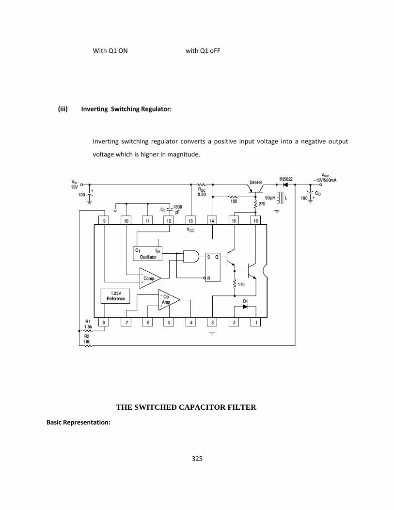
325
With Q1 ON with Q1 oFF
(iii) Inverting Switching Regulator:
Inverting switching regulator converts a positive input voltage into a negative output
voltage which is higher in magnitude.
THE SWITCHED CAPACITOR FILTER
Basic Representation:
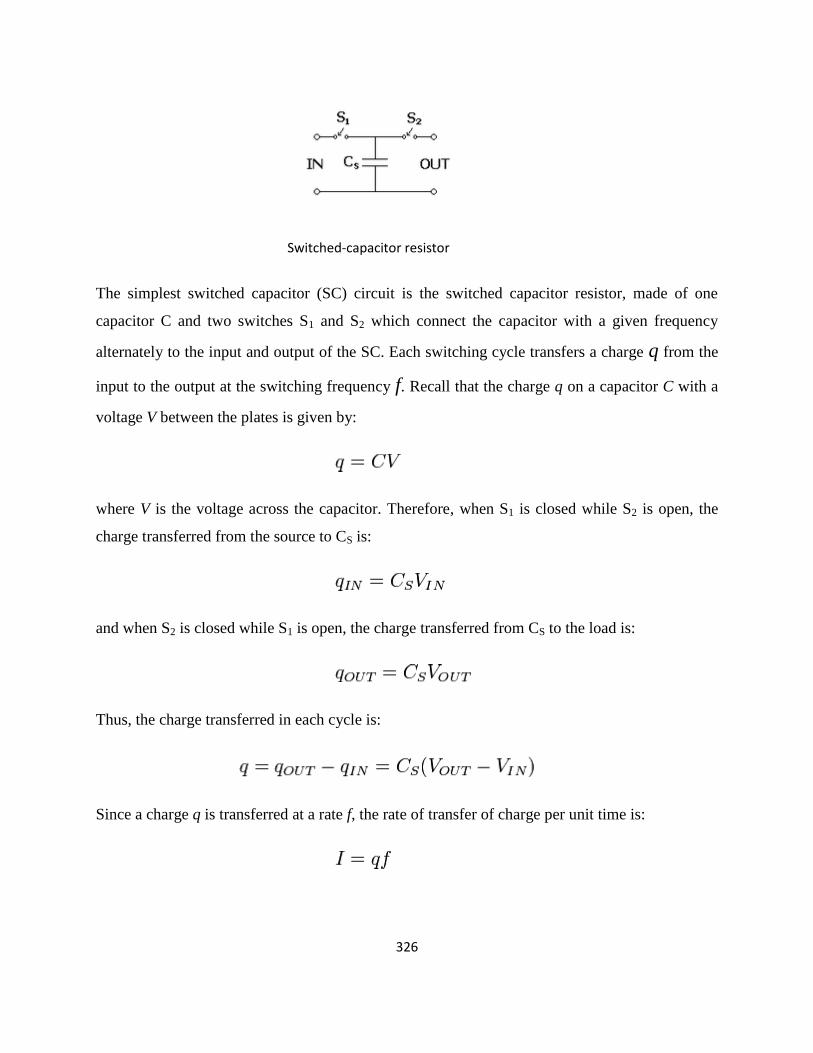
326
Switched-capacitor resistor
The simplest switched capacitor (SC) circuit is the switched capacitor resistor, made of one
capacitor C and two switches S1 and S2 which connect the capacitor with a given frequency
alternately to the input and output of the SC. Each switching cycle transfers a charge q from the
input to the output at the switching frequency f. Recall that the charge q on a capacitor C with a
voltage V between the plates is given by:
where V is the voltage across the capacitor. Therefore, when S1 is closed while S2 is open, the
charge transferred from the source to CS is:
and when S2 is closed while S1 is open, the charge transferred from CS to the load is:
Thus, the charge transferred in each cycle is:
Since a charge q is transferred at a rate f, the rate of transfer of charge per unit time is:

327
Note that we use I, the symbol for electric current, for this quantity. This is to demonstrate that a
continuous transfer of charge from one node to another is equivalent to a current. Substituting for
q in the above, we have:
Let us define V, the voltage across the SC from input to output, thus:
We now have a relationship between I and V, which we can rearrange to give an equivalent
resistance R:
Thus, the SC behaves like a resistor whose value depends on CS and f.
The SC resistor is used as a replacement for simple resistors in integrated circuits because it is
easier to fabricate reliably with a wide range of values. It also has the benefit that its value can be
adjusted by changing the switching frequency. See also: operational amplifier applications.
This same circuit can be used in discrete time systems (such as analog to digital converters) as a
track and hold circuit. During the appropriate clock phase, the capacitor samples the analog
voltage through switch one and in the second phase presents this held sampled value to an
electronic circuit for processing.
Switched Capacitor Circuits :
In the last decade or so manyactive filters with resistors and capacitors have been
replaced with a special kind of filter called a switched capacitor filter. The switched capacitor
filter allows for very sophisticated, accurate, and tuneable analog circuits to be manufactured
without using resistors. This is useful for several reasons. Chief among these is that resistors are
hard to build on integrated circuits (they take up a lot of room), and the circuits can be made to
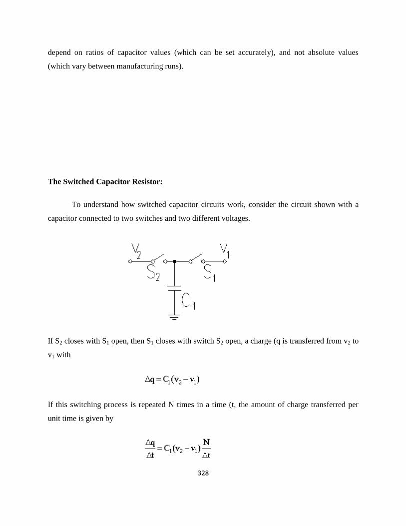
328
depend on ratios of capacitor values (which can be set accurately), and not absolute values
(which vary between manufacturing runs).
The Switched Capacitor Resistor:
To understand how switched capacitor circuits work, consider the circuit shown with a
capacitor connected to two switches and two different voltages.
If S2 closes with S1 open, then S1 closes with switch S2 open, a charge (q is transferred from v2 to
v1 with
If this switching process is repeated N times in a time (t, the amount of charge transferred per
unit time is given by

329
Recognizing that the left hand side represents charge per unit time, or current, and the the
number of cycles per unit time is the switching frequency (or clock frequency, fCLK) we can
rewrite the equation as
Rearranging we get
which states that the switched capacitor is equivalent to a resistor. The value of this resistor
decreases with increasing switching frequency or increasing capacitance, as either will increase
the amount of charge transfered from v2 to v1 in a given time.
The Switched Capacitor Integrator:
Now consider the integrator circuit. You have shown (in a previous lab) that the input-output
relationship for this circuit is given by (neglecting initial conditions):
We can also write this with the "s" notation (assuming a sinusoidal input, Aest, s=jω)
If you replaced the input resistor with a switched capacitor resistor, you would get

330
Thus, you can change the equivalent ω' of the circuit by changing the clock frequency. The
value of ω' can be set very precisely because it depends only on the ratio of C1 and C2, and not
their absolute value.
Switched Capacitor Filter Ics:
We will see some of the Switched capacitor filter Ics such as MF 5, MF10 and MF100
MF 5 :
It is the basic type of filter. This is called as universal filter because it can be used to synthesize
any type of filters such as Band pass, Low-pass, High-pass, notch and all-pass. The block
diagram of MF5 was shown here. It consists of an operational amplifier, two positive integrators
and summing node. A MOS switch is controlled by the logic input given at pin 5.
This switch is useful in connecting one of the inputs of first integrator to either ground or to the
output of the second integrator. The way in which the external resistors are connected determines
the characteristics of the filter. The maximum recommended clock frequency is 1 MHZ. There
were three modes of operation and out of all modes, mode 3 is best. All the modes have three
outputs with the combinations of different filter functions. And MF5 Can Operate with single or
split power supply. The clock frequency to center frequency ration is selected with a help of pin
9. There were two ratio options 50:1 and 100:1.

331
MF10:
The MF10 contains two of the second-order universal filter sections found in the MF5. Therefore
with MF10, two second order filters or one fourth-order filter can be built. As the MF5 and
MF10 have similar filter sections, the design procedure for them is same.

332
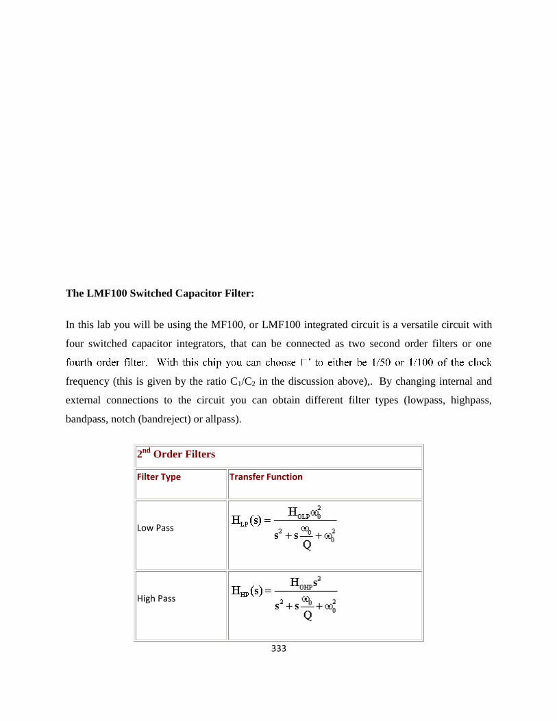
333
The LMF100 Switched Capacitor Filter:
In this lab you will be using the MF100, or LMF100 integrated circuit is a versatile circuit with
four switched capacitor integrators, that can be connected as two second order filters or one
frequency (this is given by the ratio C1/C2 in the discussion above),. By changing internal and
external connections to the circuit you can obtain different filter types (lowpass, highpass,
bandpass, notch (bandreject) or allpass).
2nd
Order Filters
Filter Type Transfer Function
Low Pass
High Pass

334
Band Pass
Notch (Band Reject)
The pinout for the LMF100 is shown below (from the data sheet):
See that the chip, for the most part, is split into two halves, left and right. A block diagram of the
left half ((and a few pins from the right half) is shown below.

335
The pins are described as
50/100 - determines if the value of ω ' is ω CLK/100, or ω CLK/50.
CLKA - is ω CLK.
INVA - the inverting input to the op-amp
N/AP/HPA - an intermediate output, and the non-inverting input to the summer. Used for
Notch, All Pass or High Pass output.
BPA - another intermediate output, the output of the first integrator. Used for Band Pass
output.
LPA - the output of the second integrator. Used for Low Pass output.
S1A - an inverting input to the summer.

336
SAB - determines if the switch is to the left or to the right. That is, this pin determines if the
second inverting input to the summer is ground (AGND), or the low pass output.
The two integrators are switched capacitor integrators. Their transfer functions are given by,
where ω' is ω CLK/100, or ω CLK/50, depending on the state of the 50/100 pin. Note that the
integrator is non-inverting.
A Typical Circuit:
The diagram below shows one of the modes (mode 1) of operations
The filter specifications as given in the datasheet, and given below.

337
The low pass (LPA) output is easily given in terms of the band pass output (BPA), as well as the
band pass output as a function of the summer (SUM, not labeled on diagram).
The summer output (SUM) is simply the output of the op amp (NA) minus the lowpass output
(LPA). However we can see that the op amp is set up as the inverting summing circuit. So
Replace SUM on the left hand side using equation (2) from above, and LPA using equation (1).

338
Rearranging brings
Equating this with the transfer function for a bandpass circuit
yields,
Similarly, the relationship between low pass and band pass, equation (1), can be used to find the
low pass transfer function. The notch filter transfer function is derived in the same way.
POWER AUDIO AMPLIFIER IC LM380:
Features of LM380:

339
1. Internally fixed gain of 50 (34dB)
2. Output is automatically self centring to one half of the supply voltage.
3. Output is short circuit proof with internal thermal limiting.
4. Input stage allows the input to be ground referenced or ac coupled.
5. Wide supply voltage range (5 to 22V).
6. High peak current capability.
7. High impedence.
8. Low total harmonic distortion
9. Bandwidth of 100KHz at Pout = 2W & RL = 8Ω
Introduction:
Small signal amplifier are essentially voltage amplifier that supply their loads with larger
amplifier signal voltage.
On the other hand , large signal or power amplifier supply a large signal current to current
operated loads such as speakers & motors.
In audio applications, however, the amplifier called upon to deliver much higher current than
that suppkied by general purpose op-amps. This means that loads such as speakers & motors requiring
substantial currents cannot be driven directly by the output of general purpose opo-amps.

340
However there are two possible solutions,
To use discrete or monolithic power transistors called power boosters at the output of the op-
amp
To use specialized ICs designed as power amplifiers.
Fig : Functional block diagram of Audio Power Amplifier

341
Fig: Pin diagram
Fig : Block diagram

342
LM380 circuit description:
It is connected of 4 stages,
(i) PNP emitter follower
(ii) Different amplifier
(iii) Common emitter
(iv) Emitter follower
(i) PNP Emitter follower:
The input stage is emitter follower composed of PNP transistors Q1 & Q2 which drives the PNP
Q3-Q4 differential pair.
The choice of PNP input transistors Q1 & Q2 allows the input to be referenced to ground i.e.,
the input can be direct coupled to either the inverting & non-inverting terminals of the
amplifier.
(ii) Differential Amplifier:
The current in the PNP differential pair Q3-Q4 is established by Q7, R3 & +V.
The current mirror formed by transistor Q7, Q8 & associated resistors then establishes the
collector current of Q9.
Transistor Q5 & Q6 constitute of collector loads for the PNP differential pair.

343
The output of the differential amplifier is taken at the junction of Q4 & Q6 transistors & is
applied as an input to the common emitter voltage gain.
(iii) Common Emitter:
Common Emitter amplifier stage is formed by transistor Q9 with D1, D2 & Q8 as a current
source load.
The capacitor C between the base & collector of Q9 provides internal compensation & helps to
establish the upper cutoff frequency of 100 KHz.
Since Q7 & Q8 form a current mirror, the current through D1 & D2 is approximately the same as
the current through R3.
D1 & D2 are temperature compensating diodes for transistors Q10 & Q11 in that D1 & D2 have
the same characteristics as the base-emitter junctions of Q11. Therefore the current through
Q10 & (Q11-Q12) is approximately equal to the current through diodes D1 & D2.
(iv) (Output stage) - Emitter follower:
Emitter follower formed by NPN transistor Q10 & Q11. The combination of PNP transistor Q11 &
NPN transistor Q12 has the power capability of an NPN transistors but the characteristics of a
PNP transistor.
The negative dc feedback applied through R5 balances the differential amplifier so that the dc
output voltage is stabilized at +V/2;
To decouple the input stage from the supply voltage +V, by pass capacitor in order of micro
farad should be connected between the by pass terminal (pin 1) & ground (pin 7).
The overall internal gain of the amplifier is fixed at 50. However gain can be increased by using
positive feedback.
APPLICATIONS:

344
(i) Audio Power Amplifier:
Amplifier requires very few external components because of the internal biasing, compensation &
fixed gain.
When the power amplifier is used in the non inverting configuration, the inverting terminal may be
either shorted to ground, connected to ground through resistors & capacitors.
Similarly when the power amplifier is used in the inverting mode, the non inverting terminal may be
either shorted to ground or returned to ground through resistor or capacitor.
Usually a capacitor is connected between the inverting terminal & ground if the input has a high
internal impedance.
As a precautionary measure, an RC combination should be used at the output terminal (pin 8) to
eliminate 5-to-10 MHz oscillation.
C1 is coupling capacitor which couples the output of the amplifier to the 8 ohms loud speaker which
act as a load. The amplifier will amplify the Vin applied at the non-inverting terminal.
(ii) LM 380 as a High gain:
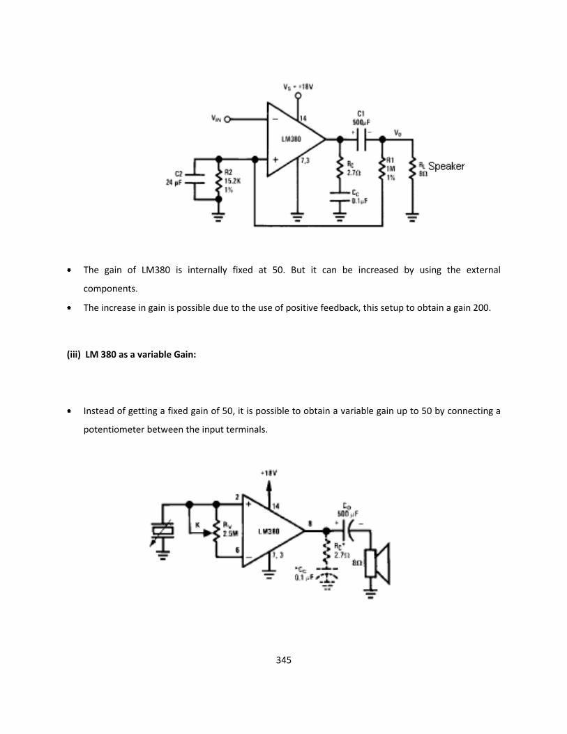
345
The gain of LM380 is internally fixed at 50. But it can be increased by using the external
components.
The increase in gain is possible due to the use of positive feedback, this setup to obtain a gain 200.
(iii) LM 380 as a variable Gain:
Instead of getting a fixed gain of 50, it is possible to obtain a variable gain up to 50 by connecting a
potentiometer between the input terminals.

346
(iv) LM 380 as a Bridge Audio Power Amplifier:
If a certain application requires more power than what is provided by a single LM380 amplifier, then
2 LM380 chips can be used in the bridge configuration.
With this arrangement we get an output voltage swing which is twice that of a single LM380
amplifier.
As the voltage is doubled, power output will increase by four times that of a single LM380 amplifier.
The pot R4 is used to balance the output offset voltages of the two chips.
(v) Intercom system using LM 380:
When the switch is in Talk mode position, the master speaker acts as a microphone.
When the switch is in Listen position, the remote speaker acts as a microphone.
In either phone the overall gain of the circuit is the same depends on the turns of transformer T.

347
Fig: Talk mode
Fig: Listen mode

348
OPTOCOUPLERS/OPTOISOLATORS:
Optocouplers or Optoisolators is a combination of light source & light detector in the same package.
They are used to couple signal from one point to other optically, by providing a completer electric
isolation between them. This kind of isolation is provided between a low power control circuit &
high power output circuit, to protect the control circuit.
Depending on the type of light source & detector used we can get a variety of optocouplers. They
are as follows,
(i) LED – LDR optocoupler
(ii) LED – Photodiode optocoupler
(iii) LED – Phototransistor optocoupler
Characteristics of optocoupler:
(i) Current Transfer Ratio (CTR)
(ii) Isolation Voltage
(iii) Response Time
(iv) Common Mode Rejection
(i) Current Transfer Ratio:
It is defined as the ratio of output collector current (Ic) to the input
forward current (If)

349
CTR = Ic/If * 100%
Its value depends on the devices used as source & detector.
(ii) Isolation voltage between input & output:
It is the maximum voltage which can exist differentially between the
input & output without affecting the electrical isolation voltage is
specified in K Vrms with a relative humidity of 40 to 60%.
(iii)Response Time:
Response time indicates how fast an optocoupler can change its output
state. Response time largely depends on the detector transistor, input
current & load resistance.
(iv)Common mode Rejection:
Eventhough the optocouplers are electrically isolated for dc & low frequency signals, an
impulsive input signal (the signal which changes suddenly) can give rise to a displacement current Ic=
Cf*dv/dt. This current can flow between input & output due to the capacitance Cf existing between
input & output. This allow the noise to appear in the output.
Types of optocoupler:

350
(i) LED – Photodiode optocoupler:
LED photodiode shown in figure, here the infrared LED acts as a light source & photodiode is used as
a detector.
The advantage of using the photodiode is its high linearity. When the pulse at the input goes high,
the LED turns ON. It emits light. This light is focused on the photodiode.

351
In response to this light the photocurrent will start flowing though the photodiode. As soon as the
input pulse reduces to zero, the LED turns OFF & the photocurrent through the photodiode reduces
to zero. Thus the pulse at the input is coupled to the output side.
(ii) LED – Phototransistor Optocoupler:

352
The LED phototransistor optocoupler shown in figure. An infrared LED acts as a light source and the
phototransistor acts as a photo detector.
This is the most popularly used optocoupler, because it does not need any additional amplification.
When the pulse at the input goes high, the LED turns ON. The light emitted by the LED is focused on
the CB junction of the phototransistor.
In response to this light photocurrent starts flowing which acts as a base current for the
phototransistor.
The collector current of phototransistor starts flowing. As soon as the input pulse reduces to zero,
the LED turns OFF & the collector current of phototransistor reduces to zero. Thus the pulse at the
input is optically coupled to the output side.
Advantages of Optocoupler:
Control circuits are well protected due to electrical isolation.
Wideband signal transmission is possible.
Due to unidirectional signal transfer, noise from the output side does not get coupled to the input
side.
Interfacing with logic circuits is easily possible.
It is small size & light weight device.
Disadvantages:
Slow speed.
Possibility of signal coupling for high power signals.
Applications:
Optocouplers are used basically to isolate low power circuits from high
power circuits.

353
At the same time the control signals are coupled from the control circuits to the high power circuits.
Some of such applications are,
(i) AC to DC converters used for DC motor speed control
(ii) High power choppers
(iii) High power inverters
One of the most important applications of an optocoupler is to couple the base driving signals to a
power transistor connected in a DC-DC chopper.
Note that the input & output waveforms are 180º out of phase as the output is taken at the
collector of the phototransistor.
Optocoupler IC:
The optocouplers are available in the IC form MCT2E is the standard optocoupler IC which is
used popularly in many electronic application.
This input is applied between pin 1& pin 2. An infrared light emitting diode is connected between
these pins.
The infrared radiation from the LED gets focused on the internal phototransistor.
The base of the phototransistor is generally left open. But sometimes a high value pull down
resistance is connected from the Base to ground to improve the sensitivity.
The block diagram shows the opto-electronic-integrated ciruit (OEIC) and the major components of
a fiber-optic communication facility.

354