EAG/Woodside Trainee and Apprenticeship Program 2015 Recruitment

EAG CAPABILITIES OVERVIEW
Engineering SciencesAram SarkissianGeneral Manager
NASA Goddard June 27, 2017
© 2017 EAG Laboratories

OVERVIEW OF EAG LABORATORIES
o EAG Laboratories Divisions:
• Engineering Sciences (“ES”): Global leader in production and engineering outsourced testing in Electrical, Reliability Stress, and Physical failure analysis services for technology customers
• Material Sciences (“MS”): Global leader in micro-analytical surface testing and analysis of materials –started as Charles Evans & Associates in 1978
• Life Sciences (“LS”): Global leader focused on technical analyses and registration requirements for the Agrochemical, Industrial Chemical, Pharmaceutical and Animal Health Industries
o EAG Laboratories is a differentiated testing and evaluation company which has a common thread across various technology and analytical services that serve different varied markets
o EAG Laboratories serves over 5,500 customers across a broad array of industries including: commercial, industrial, automotive, lighting, aerospace, LEDS, solar, biomed, pharma, chemical, agrochemical, industrial chemical, consumer and technology end markets
o >1,250 highly skilled employees worldwide, including >100 PhD scientists
EAG
Material Sciences Engineering Sciences Life Sciences
© 2017 EAG Laboratories2

ENGINEERING SERVICES
• Electrical Product Testing, Characterization and Evaluation with ATE development for volume, pilot, prototype and characterization
• Reliability Stress Testing, Qualification, Monitoring and Burn-in
• ESD and Latch-up Testing
• FIB Circuit Edit and Debug
• Full Failure Analysis Capability
• Materials Analysis
• Printed Circuit Board (PCB) Design and Hardware fabrication
We provide an integrated model that supports semiconductor / microelectronics companies in the total product lifecycle from conception to volume production
§ More than 30 years of experience in electronics industry§ Over $100M in capital equipment investment§ Quality Systems: ISO-9001 Registered, DLA Mil-883 Suitable, ISO-17025 Accredited, ITAR Registered, and Automotive
compliant with ISO/TS-16949
© 2017 EAG Laboratories 3

• Engineering expertise– Over 20 years of history providing microelectronics services with highly skilled staff– Established processes and methodology to identify root cause and deliver consistent
high quality results and services
• Large, comprehensive equipment set for increased scalability and flexibility
– Enables us to pick the right tool set / platform and location for the job– Parallel processing of large projects; scalable to handle fluctuations in demand– System redundancy to minimize impact– Capability to analyse systems down to the component level
• Multidisciplinary approach with all services under one roof + Single point of contact +“Turn-Key” offering Start-Finish
EAG Laboratories solution focus allows us to assemble the right combinationof resources to deliver optimized solutions that are timely and cost effectivethereby reducing risk
THE EAG APPROACH
© 2017 EAG Laboratories 4

ELECTRONIC TEST & MEASUREMENT (ATE)
• Production/Pilot/Prototype Testing • Hardware Design / Fabrication• Test System Rental (On site/Remote Log in)
– 24/7 access to testing and facilities– EAG engineers and expertise available on-site – System maintenance and support from in-house staff
• Test Program Development / Test Engineering• Program transfer to leading OSATs offshore• Product/Process Characterization
© 2017 EAG Laboratories 5

ATE PRODUCTION SERVICES
• Flexible production flow includes:– Daily WIP planning– Incoming Quality
inspection– Production test– Bake, dry pack, label– Outgoing Quality
inspection– Drop/Direct shipments
• WIP system for visibility
© 2017 EAG Laboratories 6

Operating/Storage Life Test– High-power Operating Life– High Temperature Operating Life– Low Temperature Operating Life– High/Low Temperature Storage
Temperature/Humidity Stress– Highly Accelerated Stress Test (HAST)– Temperature Humidity Biased– Temperature / Humidity – Temperature and Humidity Cycling
Broad set of equipment– MCC HPB-5B, 128 I/O, 32M vectors– INCAL INFINITY, 160 I/O, 16M vectors, – AEHR Max III, 96 I/O, 4M vectors – INCAL MPU, 48 I/O, 1M vectors– CRITERIA, 48 I/O, 2M vectors
RELIABILITY STRESS TESTING SERVICES
© 2017 EAG Laboratories7

Temperature Cycling– Temperature Cycling (Air to Air)– Powered Temperature Cycling– Thermal Shock (Liquid to Liquid)
Accelerated Moisture Stress– Highly Accelerated Stress Test
(Biased or Unbiased)– Autoclave up to 35 psi
Other Stresses– Package Moisture Sensitivity
Characterization– Preconditioning Flow (MSL 1-6)– Solder Reflow Simulation– Gate Leakage Test
© 2017 EAG Laboratories 8
RELIABILITY STRESS TESTING SERVICES

9
ESD & LATCH-UP CAPABILITIES
• Testing up to 2,304 Pins• Full Characterization Reports• ESD Human Body Model• ESD Machine Model• ESD Charged Device Model• Latch-up Testing To 256K Vectors• Temperature Forcing• Curve Comparisons• Multiple Systems / Multiple Locations• Talented ESD Engineering Staff • Adapter Boards for all platforms
© 2017 EAG Laboratories

10
IN-HOUSE PCB DESIGN• All design work done by EAG engineering staff• HTOL, THB, HAST, ESD, ATE designs• Multiple board design/chamber options:
– MCC– Infinity (HX, XP160)– Criteria– MPU– Trio-Tech / Hirayama– MK4
• Layout/Schematic capture• PCB pitches down to 0.3mm• Performance/Impedance matching
© 2017 EAG Laboratories

11
FIB CIRCUIT EDIT
• Design Debug• Verify Functionality• Same day prototypes for customers / engineering• Probe points / Pads • CAD Navigation / Overlay• Backside FIB / Sample Prep• Nanomachining
© 2017 EAG Laboratories
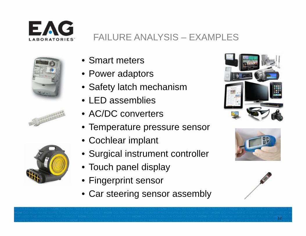
FAILURE ANALYSIS – EXAMPLES
12
• Smart meters• Power adaptors• Safety latch mechanism• LED assemblies• AC/DC converters• Temperature pressure sensor• Cochlear implant• Surgical instrument controller• Touch panel display• Fingerprint sensor• Car steering sensor assembly

FAILURE ANALYSIS – ORIGINS
13
Design, Debug, R&D•New product / design•Package assembly•Performance and function
Qualification•ESD / Latch-up•Operating Life/HALT/HAST•Environmental Stress
Production•Wafer sort yield•IC Final test yield•Yield improvement
Applications•System Level•PCB Manufacturing Yield•Field Failures
Broad analysis range from design through production and field returns
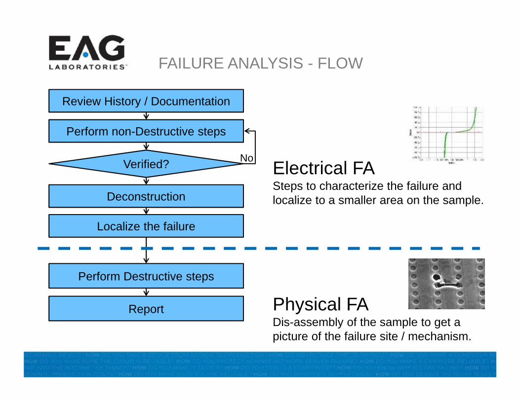
FAILURE ANALYSIS - FLOW
Review History / Documentation
Perform non-Destructive steps
Perform Destructive steps
Deconstruction
Localize the failure
Report
Electrical FASteps to characterize the failure and localize to a smaller area on the sample.
Physical FADis-assembly of the sample to get a picture of the failure site / mechanism.
Verified? No

• Analytical Services• Individual / Client driven/directed
• Turnkey FA – Level 1 – Package / Die level– Level 2 – Electrical Localization – Level 3 – Physical root cause
• Advanced FA Ø System LevelØ Root Cause
• Capabilities and Techniques• Electrical Verification / Test• Time Domain Reflectometry• X-Ray • SAM• Decap / De-lid / Sample prep• Deprocess / Cross section
• Backside Analysis• Emmi/Light Emission Microscopy• XIVA / OBIRCH• IR Thermography• Dual Beam FIB / SEM / EDS• TEM / EDS / EELS• Material Analysis / Characterization
15© 2017 EAG, Inc.
COMPONENT ANALYSIS
• Levels of Service to meet the needs of our customers

§ Advanced Device and Sample Types• Imaging/sensors: Read Output Integrated Circuit (ROIC),
Pixel Array Detector (PDA), Focal Plane Array (FPA)• Application Specific Integrated Circuit (ASIC)• Custom Hybrid Assemblies• Technology: SiGe, GaAs, InSb, InP, InGaAs, SiC, GaN• Process nodes: 28nm, 14nm FinFET• Package: Cu wire bond, Cu pillar, WLCSP, SoC, PoP,
MCM, MEMS, 3D, Stacked Devices

§ Failure Modes and Mechanisms• Functional, parametric, high leakage, excessive
sleep current, Vt shifts, dead pixels• Intermittent: manufacturing, application or
environmental factors• Fabrication: silicon crystalline, metal puddling,
photoresist/masking, misalignment, spacing, particles
• Packaging and assembly: handling, contamination,

§ Advanced Analytical Techniques• CAD Navigation / GDS file (layout and coordinates)• Dual Beam (DB FIB) slice and view• Deprocessing: advanced technology nodes (Cu, low K)• FIB Circuit Edit: probe internal nodes, modify circuit• Advanced fault isolation tools: Photon emission
(PEM/LEM/EMMI), IR thermography, Laser Signal Injection Microscopy (OBIRCH/XIVA/TIVA/LIVA).
• Backside Analysis: improved resolution, no metal masking on multi-metal layer device.)
• EDS (spot, line scan, dot mapping)• TEM

§ Investigations• Cu wire bonded PED Qualification: AEC Q006• Materials analysis: multi-discipline investigation,
critical aspect of advanced IC analysis• DOE: design of experiments (e.g. ESD, Reliability
stress, bench test failure replication, latency defects)• Modules and System or PCBA level • ESD vs. EOS• Root Cause identification: containment/corrective
actions

WHY WORK WITH EAG?
• Engineering Expertise from system level to component level with the latest technologies to address both electrical and materials characterization
• Customized Solutions that can be designed to meet your product specific and analytical support needs
• Large, comprehensive equipment set across testing and analytical services coupled with ongoing investment to address changing technological trends
• Strong integrated approach with Failure Analysis and Debug tied to ATE test, Reliability, ESD and Materials Characterizations to quickly and comprehensively develop solutions
20© 2017 EAG Laboratories