e GaN electronics: what can epitaxy enable - NMI · GaN electronics: what can epitaxy enable ......
31
IQE in Confidence Enabling Advanced Technologies GaN electronics: what can epitaxy enable nmi meeting Integrating wide bandgap and high performance silicon semiconductors into systems Cranfield University: 22 nd Oct 2015 Trevor Martin FinstP, IQE Cardiff UK
Transcript of e GaN electronics: what can epitaxy enable - NMI · GaN electronics: what can epitaxy enable ......

IQE
in C
on
fid
ence
Enabling Advanced Technologies
GaN electronics: what can epitaxy enable nmi meeting
Integrating wide bandgap and high performance silicon semiconductors into systems
Cranfield University: 22nd Oct 2015
Trevor Martin FinstP, IQE Cardiff UK

IQE
in C
on
fid
ence
Enabling Advanced Technologies 2 NMI workshop WBG & High Perf Si : Oct 2015
Outline
• IQE
• What we do
• Drivers for GaN electronics
• Technical
• Commercial
• Capability
• Products
• Development activities
• Wider perspective
• Summary

IQE
in C
on
fid
ence
Enabling Advanced Technologies 3 NMI workshop WBG & High Perf Si : Oct 2015
GaA
s b
ased
co
mp
on
ents
GSM PAs
Switch WCDMA
duplexers
WCDMA PAs
Silicon based components
IQE EPITAXY Chip Fabrication Component Assembly
Epitaxy is our business ... Engineering advanced materials

IQE
in C
on
fid
ence
Enabling Advanced Technologies GANEX summer school : June 2015
Pioneering compound semiconductor technology for over 25 years
Cardiff, UK
CVD
Milton Keynes, UK
VGF & LEC
Singapore
MBE
Cardiff, UK
MOCVD
Bath, UK
CVD: FS-GaN
Washington, USA
VGF & LEC
New Jersey, USA
MOCVD
Pennsylvania, USA
MBE & MOCVD
North Carolina, USA
MBE
Hsinchu, Taiwan
MOCVD
Massachusetts, USA
MOCVD
IQE Europe Group HQ
4

IQE
in C
on
fid
ence
Enabling Advanced Technologies 5 NMI workshop WBG & High Perf Si : Oct 2015
Drivers for GaN electronics

IQE
in C
on
fid
ence
Enabling Advanced Technologies 6 NMI workshop WBG & High Perf Si : Oct 2015
GaN power module ¼ size of GaAs equivalent
GaN for RF
SYSTEM BENEFITS Higher power density :
Smaller more compact systems Reduced weight
GaN Robustness
Higher operating temperature Robust to radiation damage
X –band telemetry transmitter launch may 2013 on Proba . > 24 months “in orbit” flight heritage
0.5dB manifold loss
4.5W 5
W
0 2 4 6 8 10 12 0 2 4 6 8 10 12
0
100
200
300
400
500
600
700
800
0 2 4 6 8 10 12
Id (
mA
/mm
) Vds (Volts)
(a) (b) (c)
25°C 500°C 300°C
• High bandgap High Temperature
• High breakdown field High Voltage
• High thermal conductivity High Power

IQE
in C
on
fid
ence
Enabling Advanced Technologies 7 NMI workshop WBG & High Perf Si : Oct 2015
GaN microwave devices
7
• Civil
• Mobile comms base-stations
• CATV
• Air traffic control and maritime radars
• Medical
• Space
• TWT & GaAs transmitter replacement
• Earth Observation (SAR)
• Navigation
• Telecoms
• Robust LNAs
• VSAT (very small aperture terminals)
• Military
• Radar
• Naval, Airborne, phased array
• EW
• Satellite communications

IQE
in C
on
fid
ence
Enabling Advanced Technologies 8 NMI workshop WBG & High Perf Si : Oct 2015
GaN for Power Control
• What differentiates GaN in Power control • Significant Size and weight benefits
• Higher frequency c.f. silicon enables smaller passives and filters
• Higher efficiency
• reduces cooling requirements
• Wider band gap allows
• higher temperature operation
8

IQE
in C
on
fid
ence
Enabling Advanced Technologies 9 NMI workshop WBG & High Perf Si : Oct 2015
DC-DC
Server
/ looter
note
PC
Li+ batt
Comms
Power
supply HDD
HEV, EV
inverter
Switching PS
server / WS
AC adaptor
DC-DC
convertor
Automobile
EPS
ABS
Injector
Industrial
inverter
Aircon
Fridge
Traction
power
transmission
GaN Power Control – Market
9

IQE
in C
on
fid
ence
Enabling Advanced Technologies 10 NMI workshop WBG & High Perf Si : Oct 2015
DC-DC
Server
/ looter
note
PC
Li+ batt
Comms
Power
supply HDD
HEV, EV
inverter
Switching PS
server / WS
AC adaptor
DC-DC
convertor
Automobile
EPS
ABS
Injector
Industrial
inverter
Aircon
Fridge
Traction
power
transmission
SiC
Silicon
GaN Power Control – Market
10
GaN
M Kanechika Toyota, IEDM 2010

IQE
in C
on
fid
ence
Enabling Advanced Technologies 11 NMI workshop WBG & High Perf Si : Oct 2015
Capability

IQE
in C
on
fid
ence
Enabling Advanced Technologies 12 NMI workshop WBG & High Perf Si : Oct 2015
Current capability
RF Power Control
SiC substrate 100 and 150mm
Silicon substrate
100 and 150mm
High Resistivity Float zone Silicon
100, 150 and 200mm
Conducting Czochralski Silicon

IQE
in C
on
fid
ence
Enabling Advanced Technologies 13 NMI workshop WBG & High Perf Si : Oct 2015
Project activities

IQE
in C
on
fid
ence
Enabling Advanced Technologies 14 NMI workshop WBG & High Perf Si : Oct 2015
RF GaN on Silicon Carbide (100mm dia)
SiC Substrate
GaN “buffer”
AlGaN barrier 2DEG / Channel
0 50 100 150 200 250 300 350 µm
µm
0
50
100
150
200
250
300
350
nm
0
2
4
6
8
10
12
14
16
18
20
22
24
26
28
X polarisor Transmission
SIMS : Fe
Surface Topography
X-ray
C-V
Curvature
(004) omega-2 theta Scan
GaN
AlGaN
SiC Sheet Resistivity

IQE
in C
on
fid
ence
Enabling Advanced Technologies 15 NMI workshop WBG & High Perf Si : Oct 2015
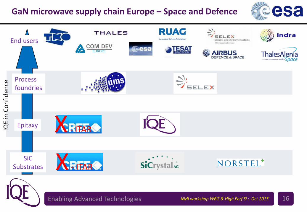
GaN microwave supply chain Europe – Space and Defence
SiC Substrates
Epitaxy
Process foundries
End users
IQE
in C
on
fid
ence
Enabling Advanced Technologies 16 NMI workshop WBG & High Perf Si : Oct 2015
GaN microwave supply chain Europe – Space and Defence
SiC Substrates
Epitaxy
Process foundries
End users
X - ITAR
X - ITAR

IQE
in C
on
fid
ence
Enabling Advanced Technologies 17 NMI workshop WBG & High Perf Si : Oct 2015
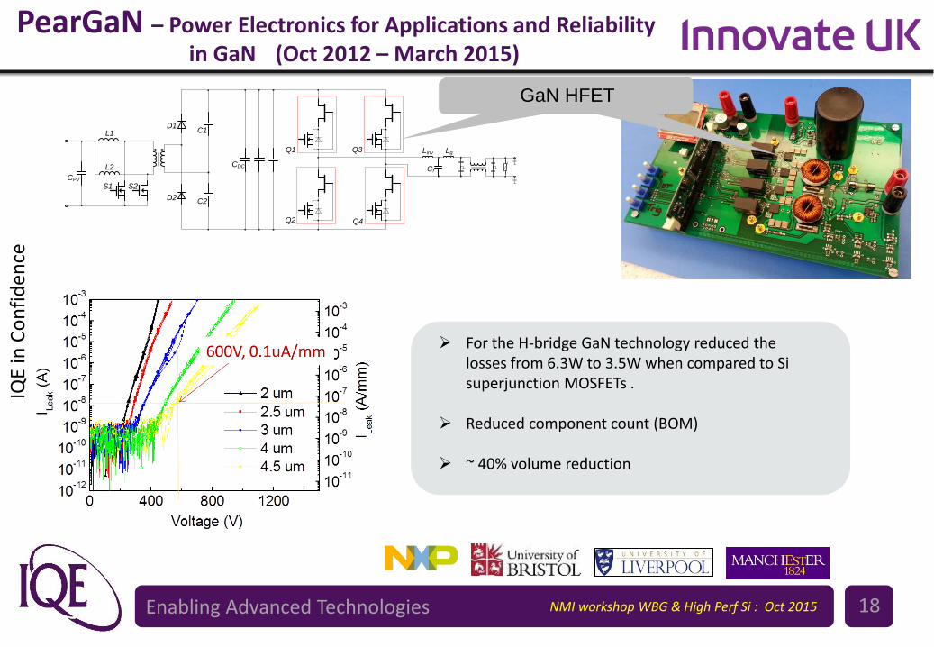
PearGaN – Power Electronics for Applications and Reliability in GaN (Oct 2012 – March 2015)
• Motivation • The world is moving to an ever increasing demand for power conversion
• “All electric” - Diversification in energy generation and increased sensors and actuators in domestic and industrial applications
• Conversion efficiency using Si devices is reaching a limit • Si CoolMOS (Super Junction MOSFET)
• GaN can surpass this
• Lateral H-FET
• Small individual savings – but large impact because of volume • GaN has potential to increase conversion efficiency by 2% (96% - 98%)
• UK data centres use ~3GW 1 • 2% over a year is equivalent to consumption of ~100,000 households 2 (Borough of Swindon)
• Excellent compatibility with existing Si processes • Thin < 10micron GaN layer on a Silicon substrate
• “Looks like Silicon”
• 150 and 200mm wafer diameter • Compatible with Si foundries
17
1 DatacentreDynamics global census 2012 2 UK Dpt Energy & Climate Change 2014
BIS: “Power Electronics a strategy for success”: Oct 2011
IQE
in C
on
fid
ence
Enabling Advanced Technologies 18 NMI workshop WBG & High Perf Si : Oct 2015
PearGaN – Power Electronics for Applications and Reliability in GaN (Oct 2012 – March 2015)
Q1
Q2
Q3
Q4
CDC
C1
C2
D1
D2
S2S1
L1
L2
CPV
Linv
Cf
Lg
GaN HFET GaN HFET
For the H-bridge GaN technology reduced the losses from 6.3W to 3.5W when compared to Si superjunction MOSFETs .
Reduced component count (BOM)
~ 40% volume reduction

IQE
in C
on
fid
ence
Enabling Advanced Technologies 19 NMI workshop WBG & High Perf Si : Oct 2015
KTP: Dynamic characteristics
• Combine • Measurement
• Back-bias sweeps to replicate vertical fields
• Different buffer structures
• Modelling Silvaco-Atlas
• Better understand where charges are trapped & move
Current
Time

IQE
in C
on
fid
ence
Enabling Advanced Technologies 20 NMI workshop WBG & High Perf Si : Oct 2015
Wider perspective

IQE
in C
on
fid
ence
Enabling Advanced Technologies 21 NMI workshop WBG & High Perf Si : Oct 2015
GaN on Si for RF : 200mm process in a Silicon CMOS Foundry
200mm
GaN/Si
HEMT
Ref: LaRoche et al CS MANTECH 2014

IQE
in C
on
fid
ence
Enabling Advanced Technologies 22 NMI workshop WBG & High Perf Si : Oct 2015
GaN on Si for RF
2014

IQE
in C
on
fid
ence
Enabling Advanced Technologies 23 NMI workshop WBG & High Perf Si : Oct 2015
E-mode Power devices on 200mm Si
“D-mode “ – Normally on basis of initial development normally off in “cascode” configuration “E-mode” - Normally off

IQE
in C
on
fid
ence
Enabling Advanced Technologies 24 NMI workshop WBG & High Perf Si : Oct 2015
Higher Frequency applications of GaN – DARPA “NEXT” / HRL
• The single chip MMIC peak output power level of 842 mW at 88 GHz (14 V bias) Micovic et al., IEEE Int. Microw. Symp. Dig., pp. 237-239, 2010.
20-nm-gate E-mode HEMTs with an increased Lsw of 70 nm demonstrated a simultaneous fT/fmax of 342/518 GHz with an off-state breakdown voltage of 14V.
Goal: 1000-transistor, high-yield, 500 GHz E/D-mode GaN technology for mixed signal applications

IQE
in C
on
fid
ence
Enabling Advanced Technologies 25 NMI workshop WBG & High Perf Si : Oct 2015
Final Thought

IQE
in C
on
fid
ence
Enabling Advanced Technologies 26 NMI workshop WBG & High Perf Si : Oct 2015
GaN/Si Can Leverage Tremendous Scale
Question: How many 200mm equivalent silicon wafers were consumed worldwide in CY2013?
Answer: More than 180,000,000
Reference: a.) SEMI Manufacturers Group
(a)

IQE
in C
on
fid
ence
Enabling Advanced Technologies 27 NMI workshop WBG & High Perf Si : Oct 2015
GaN/Si Can Leverage Tremendous Scale
Question: How many 200mm equivalent silicon wafers were consumed worldwide in CY2013?
Answer: More than 180,000,000
Reference: a.) SEMI Manufacturers Group
37 weeks o/p generates enough wafers to cover 4 square km of Cranfield
(a)

IQE
in C
on
fid
ence
Enabling Advanced Technologies 28 NMI workshop WBG & High Perf Si : Oct 2015
Summary
• GaN is very compatible with Si • RF applications • Power control applications
• 200mm dia wafers for volume applications • Depletion mode (normally on) • Enhancement mode (normally off) • High frequency – upto 400GHz • Mixed signal (A-D)
• Harsh environments (Niche) • GaN on SiC option

IQE
in C
on
fid
ence
Enabling Advanced Technologies 29 NMI workshop WBG & High Perf Si : Oct 2015
Questions Thank you

IQE
in C
on
fid
ence
Enabling Advanced Technologies 30 NMI workshop WBG & High Perf Si : Oct 2015
Developments IQE/cardiff uni
30

IQE
in C
on
fid
ence
Enabling Advanced Technologies 31 NMI workshop WBG & High Perf Si : Oct 2015
Developments IQE/cardiff uni
Research Institute in Compound
Semi’
TRL 1-3
Compound Semi’
Foundation “CSF”
TRL 4-6
CS Epi Foundry Underpinning
EU supply chain ECSEL
(EFFORTLESS)
TRL6-8