
Dysprosium-doped cadmium oxide as a gateway · PDF fileA gateway material for mid-infrared...
12
SUPPLEMENTARY INFORMATION DOI: 10.1038/NMAT4203 NATURE MATERIALS | www.nature.com/naturematerials 1 Edward Sachet 1 , Christopher T. Shelton 1 , Joshua S. Harris 1 , Benjamin E. Gaddy 1 , Douglas L. Irving 1 , Stefano Curtarolo 2 , Brian F. Donovan 3 , Patrick E. Hopkins 4 , Peter A. Sharma 5 , Ana Lima Sharma 5 , Jon Ihlefeld 5 , Stefan Franzen 6 and Jon-Paul Maria 1 1 Department of Materials Science, North Carolina State University, Raleigh, North Carolina 27695, USA 2 Dept. of Mechanical Engineering and Materials Science and Dept. Electrical Engineering, Duke University, Durham, North Carolina 27708, USA 3 Dept. of Materials Science and Engineering, University of Virginia, Charlottesville, Virginia 22904, USA 4 Dept. of Mechanical and Aerospace Engineering, University of Virginia, Charlottesville, Virginia 22904, USA 5 Sandia National Laboratories, Albuquerque, New Mexico 87185, USA 6 Department of Chemistry, North Carolina State University, Raleigh, North Carolina 27695, USA Supplementary information Figure 1. Transport data for CdO:Dy grown on MgO (111) substrates summarizing carrier conc. (cm -3 ) and carrier mobility (μ) as a function of [Dy]. Dysprosium-doped cadmium oxide as a gateway material for mid-infrared plasmonics © 2015 Macmillan Publishers Limited. All rights reserved
Transcript of Dysprosium-doped cadmium oxide as a gateway · PDF fileA gateway material for mid-infrared...

SUPPLEMENTARY INFORMATIONDOI: 10.1038/NMAT4203
NATURE MATERIALS | www.nature.com/naturematerials 1
1
Dysprosium doped cadmium oxide: A gateway material for mid-infrared plasmonics
Edward Sachet1, Christopher T. Shelton1, Joshua S. Harris1, Benjamin E. Gaddy1, Douglas L. Irving1,
Stefano Curtarolo2, Brian F. Donovan3, Patrick E. Hopkins4, Peter A. Sharma5, Ana Lima Sharma5, Jon Ihlefeld5, Stefan Franzen6 and Jon-Paul Maria1
1Department of Materials Science, North Carolina State University, Raleigh, North Carolina 27695, USA
2Dept. of Mechanical Engineering and Materials Science and Dept. Electrical Engineering, Duke University, Durham, North Carolina 27708, USA 3Dept. of Materials Science and Engineering, University of Virginia, Charlottesville, Virginia 22904, USA
4Dept. of Mechanical and Aerospace Engineering, University of Virginia, Charlottesville, Virginia 22904, USA 5Sandia National Laboratories, Albuquerque, New Mexico 87185, USA
6Department of Chemistry, North Carolina State University, Raleigh, North Carolina 27695, USA
Supplementary information
Figure 1. Transport data for CdO:Dy grown on MgO (111) substrates summarizing carrier conc. (cm-3) and carrier mobility (μ) as a function of [Dy].
Dysprosium-doped cadmium oxide as a gateway material for mid-infrared plasmonics
© 2015 Macmillan Publishers Limited. All rights reserved

2 NATURE MATERIALS | www.nature.com/naturematerials
SUPPLEMENTARY INFORMATION DOI: 10.1038/NMAT4203
2
Figure 2. Transport data for CdO:Dy grown on GaN (002) substrates summarizing carrier conc. (cm-3) and carrier mobility (μ) as a function of [Dy].
Figure 3. Transport data for CdO:Dy grown on Al2O3 (006) substrates summarizing carrier conc. (cm-3) and carrier mobility (μ) as a function of [Dy].
© 2015 Macmillan Publishers Limited. All rights reserved

NATURE MATERIALS | www.nature.com/naturematerials 3
SUPPLEMENTARY INFORMATIONDOI: 10.1038/NMAT4203
3
Figure 4. XRD diffraction patterns depicting heteroepitaxial growth of CdO on MgO (100) substrates. a) Diffraction pattern for single phase CdO:Dy samples. This growth habit is exemplary for Dy contents from 0-5x1021 cm-3. b) Growth habit for samples with Dy content >5x1021 cm-3. The precipitation of additional complex oxide phases can be seen around 30° 2θ.
Figure 5. FWHM of X-ray omega rocking curves recorded for CdO:Dy grown on MgO (100) substrates compared to the measured carrier mobilities as a function of [Dy]. No significant change in crystal quality is observed over the high mobility range, the deteriorating FWHM and mobility at the highest [Dy] corresponds to the onset of phase separation as the solubility limit of Dy in CdO is reached
© 2015 Macmillan Publishers Limited. All rights reserved

4 NATURE MATERIALS | www.nature.com/naturematerials
SUPPLEMENTARY INFORMATION DOI: 10.1038/NMAT4203
4
Figure 6. Calculated real (solid lines) and imaginary (dashed lines) dielectric functions for selected CdO:Dy alloys. The compositionally tunable SPR in CdO:Dy can be seen by the changing cross-over frequency of the real dielectric function (the energy at which the real part of ε becomes negative) for different carrier concentrations. In addition, the loss tangent (imaginary part of ε) exhibits very low values across the mid-IR energy range for all carrier concentrations depicted, indicating the potential for low loss plasmonic resonances in this material. Table 1. A comparison of plasmonic materials discussed in this article. The crossover frequency ε1=0 describes the upper frequency limit for plasmonic phenomena in a material. The loss tangent ε2 was summarized at and below (ε1=-2) the crossover frequency to allow for a comparison of losses independent of the carrier concentrations and thus the supported plasmon wavelengths.
Material
Carriers
[cm-3] Mobility
[cm2/V·s] ε1=0 [cm-1]
ε2 at ε1=0
ε2 at ε1=-2
CdO:Dy 9.94x10¹⁹ 474 2770 0.19 0.30 CdO:Dy 3.70x10²⁰ 359 5350 0.13 0.20
AZO (2 wt%)4 7.2x10²⁰ 48 6970 0.21 0.39 ITO (10 wt%)4 7.7x10²⁰ 36 7122 0.69 1.29
GaAs* 1x10¹⁹ 1000 1005 1.26 1.63 InAs9 7.5x10¹⁹ 360 1785 2.00 2.60
*Szmyd, D. M., Hanna, M. C. & Majerfeld, A. Heavily doped GaAs:Se. II. Electron mobility. J. Appl. Phys. 68, 2376–2381 (1990).
© 2015 Macmillan Publishers Limited. All rights reserved

NATURE MATERIALS | www.nature.com/naturematerials 5
SUPPLEMENTARY INFORMATIONDOI: 10.1038/NMAT4203
5
Figure 7. High resolution SEM surface image depicting the cubic growth habit in atomically smooth CdO:Dy films.
Supplementary methods:
Densitiy functional theory:
DFT calculations were performed with the Vienna Ab initio Simulation Package (VASP) version 5.3, using
the hybrid exchange correlation functional of Heyd, Scuseria, and Ernzerhof (HSE06). The atoms were
represented by the standard Purdue-Burke-Ernzerhof projector-augmented wave (PBE-PAW)
pseudopotentials included with VASP. The Cd pseudopotential includes 12 valence electrons explicitly
modeled (4d10 5s2) and has a recommended minimum energy cutoff of 274.34 eV. The O pseudopotential
includes 6 valence electrons (2s2 2p4) with a minimum energy cutoff of 400 eV. The Dy pseudopotential
includes 20 valence electrons (4f10 5s2 5p6 6s2) with a minimum energy cutoff of 255.47 eV. An energy cutoff
of 520 eV (1.3 times the recommended cutoff for the O pseudopotential) was employed in all calculations.
The defect calculations were based on 64-atom supercells with a 2x2x2 k-point mesh using the Monkhorst-
Pack formalism. The k-points were unshifted in reciprocal space and do not include the Gamma point. In the
defective supercells, atoms near the defect site were allowed to relax within a spherical shell out to the third
nearest neighbor of the defect site, while all other atoms were frozen in their bulk positions. The
displacements of the farthest atoms from the defect site (3rd nearest neighbor sites) within this relaxation shell
were on the order of 0.001 Angstrom as opposed to 0.01 Angstrom for the 1st and 2nd nearest neighbor sites
(cf. Table 1 in the article), indicating that the shell size was large enough to account for most of the crystal
strain resulting from the presence of the defect. Finite size interactions for the charged defects were accounted
© 2015 Macmillan Publishers Limited. All rights reserved

6 NATURE MATERIALS | www.nature.com/naturematerials
SUPPLEMENTARY INFORMATION DOI: 10.1038/NMAT4203
6
for using the sxdefectalign code by Christoph Freysoldt. This was the only correction applied to the calculated
defect formation energies.
The defect and carrier concentrations were calculated via solutions to the mass and charge balance equations,
using the DFT formation energies and charge transitions as inputs. The effect of dysprosium concentration,
[DyCd], on the concentrations of native defects and carriers was explored for a variety of growth conditions
(oxygen and cadmium chemical potentials). This was done through iterative solutions of the mass and charge
balance equations to determine the Fermi energy over a range of fixed concentrations of Dy. At each
concentration, the Dy chemical potential was adjusted in order to constrain the substituent to the targeted
amount. The Dy chemical potentials required to fix each Dy concentration were analyzed to confirm that they
were thermodynamically accessible. This approach to solving the mass balance equations requires no a priori
assumptions as to which defects are ionized. Using this method, the equilibrium defect concentrations were
calculated at the growth temperature (623 K). Then, simulating a quench, the high temperature defect
concentrations were frozen in at the growth temperature. At room temperature, the carriers were allowed to
redistribute via movement of the Fermi level to satisfy charge neutrality. In this manner, the plot presented in
the article, showing O-vacancy and carrier concentrations versus Dy-substituent concentration at different O-
chemical potentials, was created.
Time domain thermo reflectance (TDTR):
The thermal conductivity of various CdO:Dy samples were measured using time domain thermoreflectance
(TDTR).1,4,6 TDTR is an optical pump-probe experiment which utilizes a train of ultrashort laser pulses to
induce a modulated heating event on the sample surface and monitor the resulting thermal decay. For these
TDTR measurements, we coat the samples with an 83±3 nm aluminum film, which acts as a thermal
transducer to relate the absorbed pump energy to the temporal temperature change on the samples surface.
Our specific TDTR system is centered around a sub-picosecond Ti:Sapphire oscillator. We sinusoidally
modulate the pump pulses at 8.8 MHz using an electro-optic modulator. The probe is delayed through time up
to 6.5 ns by a mechanical delay stage. The pump and probe are focused onto the sample by a converging lens
with spot diameters of 42 µm and 11 µm, respectively. The large pump spot size ensures that no significant
radial heat spread occurs in the sample that that heat propagation is nearly one-dimensional.4 Using a lock-in
amplifier, we isolate the thermoreflectance signal of the sample via detection of the modulated response of the
probe referenced to the pump modulation. The change in surface temperature of the sample is directly related
to the change in the ratio of the in-phase and out-of-phase components of the detected lock-in signal over the
change in time delay between the pump and probe. The data is compared to a thermal model that represents
the solution of the heat diffusion equation in a multilayer system. Details of this model are provided
elsewhere.1,4,6 In our analysis, we assume literature values for the heat capacity of the Al3, CdO5, MgO2 and
thermal conductivity of the MgO7 as well. The major source of error in our analysis arrises from uncertainty
© 2015 Macmillan Publishers Limited. All rights reserved

NATURE MATERIALS | www.nature.com/naturematerials 7
SUPPLEMENTARY INFORMATIONDOI: 10.1038/NMAT4203
7
in the thickness of the Al transducer. To minimize this uncertainty, we verify the Al film thickness with both
X-ray reflectivity and picosecond acoustic analysis.8,9
Figure 8. Data and best-fit curve of TDTR data for undoped CdO
Figure 8 shows the data and best-fit curve of our model for the TDTR measurement of the undoped CdO
sample. To ensure that our model is sensitive to the properties that we are fitting, we perform sensitivity
analysis on the main parameters used in our thermal model.10,11 The sensitivity, S, to a certain thermo-physical
property, p, is defined by:
Sp = ∂ln(-Vin /Vout )∂ln(p)
(1)
Where Vin and Vout are the in-phase and out-of-phase responses components of the thermoreflectance signal
from the lock-in amplifier. Degree of sensitivity to a property is determined by the relative magnitude of the
sensitivity parameter over the measurement time. Figure 9, show the sensitivity to the thermal boundary
© 2015 Macmillan Publishers Limited. All rights reserved

8 NATURE MATERIALS | www.nature.com/naturematerials
SUPPLEMENTARY INFORMATION DOI: 10.1038/NMAT4203
8
conductance between the Al transducer and the undoped CdO film, h1, the thermal boundary conductance
between the CdO and the MgO, h2, and the sensitivity to the thermal conductivity of the Al, κAl, CdO, κCdO,
and MgO, κMgO. In our system, we are most sensitive to the thermal conductivity of the CdO layer and h1.
These two parameters are treated as free parameters in the fitting of our data to the thermal model.
Figure 9. Sensitivity to the thermal boundary conductance between the Al transducer and the undoped CdO film, h1, the thermal boundary conductance between the CdO and the MgO, h2, and the sensitivity to the thermal conductivity of the Al (κAl), CdO (κCdO), and MgO (κMgO).
References:
1. David G. Cahill. Analysis of heat flow in layered structures for time-domain thermoreflectance. Review of Scientific Instruments, 75(12):5119–5122, 2004.
2. M.W. Chase. Nist-janaf thermochemical tables. In Jouranl of Physical and Chemical Reference Data, volume Part 1. National Institute of Standards and Technology, fourth edition, 1998.
3. G.T. Furukawa, M.L. Reilly, and J.S. Gallagher. Critical analysis of heat-capacity data and evaluation of thermodynamic properties of ruthenium, rhodium,palladium, iridium, and platinum from 0 to 300 k. Journal of Physical and Chemical Reference Data, 3, 1974.
4. Patrick E. Hopkins, Justin R. Serrano, Leslie M. Phinney, Sean P. Kearney, Thomas W. Grasser, and C. Thomas Harris. Criteria for
© 2015 Macmillan Publishers Limited. All rights reserved

NATURE MATERIALS | www.nature.com/naturematerials 9
SUPPLEMENTARY INFORMATIONDOI: 10.1038/NMAT4203
9
cross-plane dominated thermal transport in multilayer thin film systems during modulated laser heating. Journal of Heat Transfer, 132(8):081302–081302, 05 2010.
5. O. Madelung, U. Rössler, and M. Schulz. Cadmium oxide (cdo) debye temperature, heat capacity, melting point, density. In O. Madelung, U. Rössler, and M. Schulz, editors, II-VI and I-VII Compounds; Semimagnetic Compounds, volume 41B of Landolt-Börnstein - Group III Condensed Matter, pages 1–3. Springer Berlin Heidelberg, 1999.
6. Aaron J. Schmidt, Xiaoyuan Chen, and Gang Chen. Pulse accumulation, radial heat conduction, and anisotropic thermal conductivity in pump-probe transient thermoreflectance. Review of Scientific Instruments, 79(11):114902, 2008.
7. Glen A. Slack. Thermal conductivity of mgo, al2o3, mgal2o4, and fe3o4 crystals from 3to 300k. Phys. Rev., 126:427–441, Apr 1962.
8. C. Thomsen, H. T. Grahn, H. J. Maris, and J. Tauc. Surface generation and detection of phonons by picosecond light pulses. Phys. Rev. B, 34:4129–4138, Sep 1986.
9. C. Thomsen, J. Strait, Z. Vardeny, H. J. Maris, J. Tauc, and J. J. Hauser. Coherent phonon generation and detection by picosecond light pulses. Phys. Rev. Lett., 53:989–992, Sep 1984.
10. Ruxandra M. Costescu, Marcel A. Wall, and David G. Cahill. Thermal conductance of epitaxial interfaces. Phys. Rev. B, 67:054302, Feb 2003.
11. Patrick E. Hopkins, Leslie M. Phinney, Justin R. Serrano, and Thomas E. Beechem. Effects of surface roughness and oxide layer on the thermal boundary conductance at aluminum/silicon interfaces. Phys. Rev. B, 82:085307, Aug 2010.
Supplementary Equations:
Reflectivity model based on a free electron Drude plasma:
To model the dielectric constant of the CdO films, a free electron Drude model was used. In this model, the
real (εr) and imaginary (εi) dielectric functions are given by Eq. (1) and (2)
𝜀𝜀! = 𝜀𝜀! −𝜔𝜔!!
𝜔𝜔! + 𝛾𝛾! (1)
𝜀𝜀! =𝛾𝛾𝜔𝜔!!
𝜔𝜔(𝜔𝜔! + 𝛾𝛾!) (2)
where 𝜔𝜔! is the plasma frequency (Eq. 3), 𝜀𝜀! is the high frequency dielectric constant and 𝛾𝛾 is a damping
term (Eq. 4).
𝜔𝜔!! =𝑛𝑛𝑞𝑞!
𝑚𝑚!𝜀𝜀! (3)
𝛾𝛾 =𝑞𝑞
𝜇𝜇𝑚𝑚! (4)
The plasma frequency is directly dependent on the carrier density (𝑛𝑛) where 𝑞𝑞 is the electron charge
(1.602×10⁻¹⁹C), 𝜀𝜀! is the permittivity of free space, 𝑚𝑚! is the effective electron mass and 𝜇𝜇 is the electron
mobility. For CdO a 𝑚𝑚! of 0.21 and 𝜀𝜀! of 5.5 have been used. The reflectance at an interface was described
by the Fresnel equations:
© 2015 Macmillan Publishers Limited. All rights reserved

10 NATURE MATERIALS | www.nature.com/naturematerials
SUPPLEMENTARY INFORMATION DOI: 10.1038/NMAT4203
10
𝑟𝑟! =𝑛𝑛! cosΘ! − 𝑛𝑛! cosΘ!𝑛𝑛! cosΘ! + 𝑛𝑛! cosΘ!
(5)
𝑟𝑟! =𝑛𝑛! cosΘ! − 𝑛𝑛! cosΘ!𝑛𝑛! cosΘ! + 𝑛𝑛! cosΘ!
(6)
where the complex refractive indices of the incident material (𝑛𝑛!) and the transmitted material (𝑛𝑛!) together
with the incident angle Θ are used to calculate the reflectance for both p- and s-polarized light. To calculate
the refractive index of the modeled film, the relation 𝑛𝑛 = 𝜀𝜀 ! was used.
The total reflectance from the substrate/CdO/air interface can be calculated using the Airy formula
𝑟𝑟 =𝑟𝑟! + 𝑟𝑟!exp (2𝑖𝑖𝑖𝑖)1 + 𝑟𝑟!𝑟𝑟! exp 2𝑖𝑖𝑖𝑖
(7)
with
𝑏𝑏 =2𝜋𝜋𝑑𝑑!𝜆𝜆
𝑛𝑛!"#$! − 𝑛𝑛!"#!$%&$'! sin! Θ! (8)
where 𝜆𝜆 is the incident light wavelength, 𝑑𝑑! is the film’s thickness and 𝑟𝑟! and 𝑟𝑟! are the calculated
reflectances from interface 1 and 2. Additionally, the back reflection from the CaF2/substrate interface was
calculated using Eq. 5-6 and added to the calculated reflectivity data. The data is ultimately compiled into
maps of the total reflectance in angle and wavenumber space (Eq. 9).
𝑅𝑅 =𝑅𝑅!𝑅𝑅!
=𝑟𝑟!
!
𝑟𝑟! ! (9)
To account for the strong dispersion in the mid-IR of all optical elements used in the recording of the
reflectivity data (substrates, prism), the dielectric dispersion of these materials was included in the
calculations.
Origin of strong vertical (angle independent) absorption lines in experimental SPR data.
The observed strong spectral features at 1350 cm-1 are a consequence of a dark band in the IR-VASE source
output. A raw spectrum of the output spectra is depicted in Figure 10. Due to the dim and noisy nature of the
ellipsometers output at these frequencies, the absolute recorded intensity at these energies is low and the
Rp/Rs representation of the data amplifies the noisy band. It is important to note that this is a measurement
artifact caused by the spectrometers radiation source, and the artifact does not show any angle dependency.
Thus, it does not limit the data’s validity for characterizing the SPP dispersion in the mid-IR. Since our
simulations assume even intensity for the radiation over the frequency range of interest, this experimental
detail is not included in the simulated data. Experimentally, the data is normalized to the background
spectrum, as typically done for fourier transform IR spectrometers.
© 2015 Macmillan Publishers Limited. All rights reserved

NATURE MATERIALS | www.nature.com/naturematerials 11
SUPPLEMENTARY INFORMATIONDOI: 10.1038/NMAT4203
11
Figure 10. Raw source output spectrum of the IR-VASE ellipsometer used for this work. A dark band can be seen
around 1350 cm-1 for both polarization directions used in this work. This dark band is the origin of the spectral
feature seen in Figure 3 in the article.
SPP quality factor calculations:
Propagation length:
The propagation length Lω for a single metal/dielectric interface was calculated as1:
Lω =1/ (ωc
εrεr +1
)
The confinement width Dω is defined as1 :
© 2015 Macmillan Publishers Limited. All rights reserved
12 NATURE MATERIALS | www.nature.com/naturematerials
SUPPLEMENTARY INFORMATION DOI: 10.1038/NMAT4203
12
Dω =1
ωc
−1εr +1
+ ( 1ωc
−εr2
εr +1
)(1− Log εr )
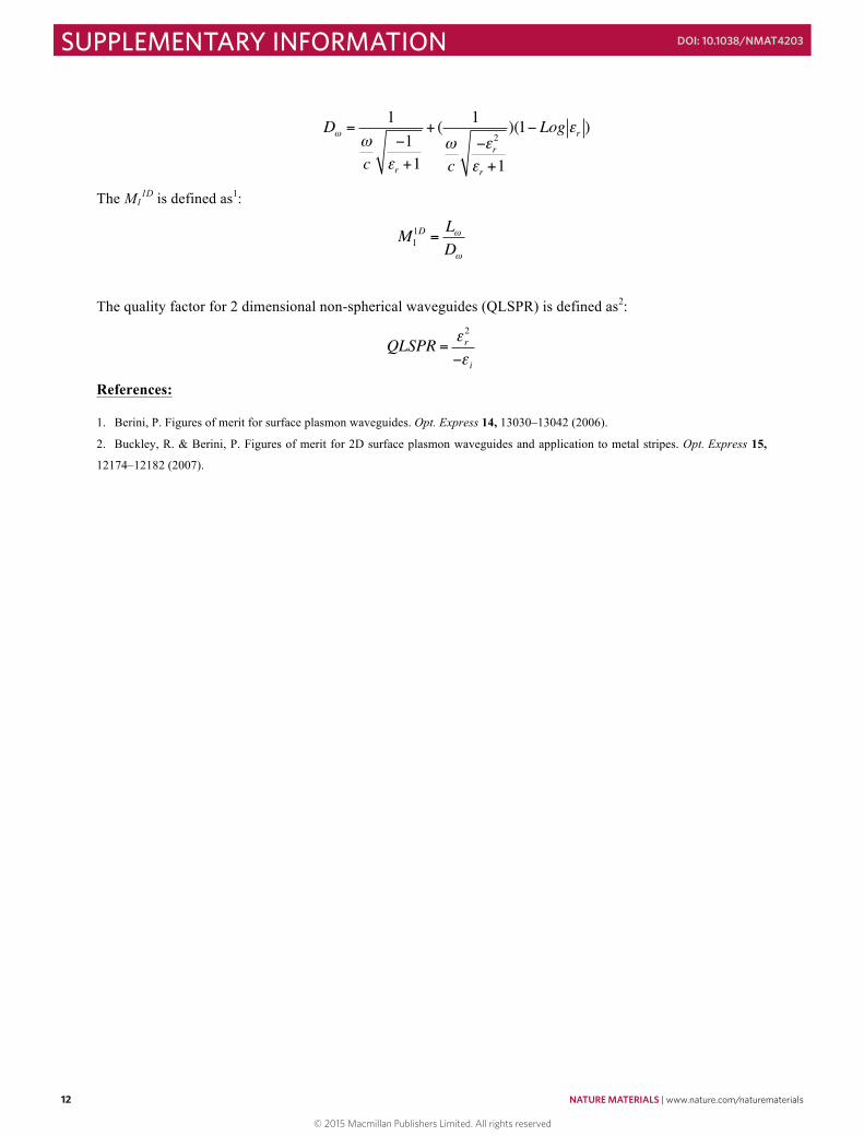
The M11D is defined as1:
M11D =
LωDω
The quality factor for 2 dimensional non-spherical waveguides (QLSPR) is defined as2:
QLSPR = ε 2r−ε i
References:
1. Berini, P. Figures of merit for surface plasmon waveguides. Opt. Express 14, 13030–13042 (2006).
2. Buckley, R. & Berini, P. Figures of merit for 2D surface plasmon waveguides and application to metal stripes. Opt. Express 15,
12174–12182 (2007).
© 2015 Macmillan Publishers Limited. All rights reserved