Dynamically Reconfigurable PWM Controller for Three...
40
1790 IEEE TRANSACTIONS ON POWER ELECTRONICS, VOL. 26, NO. 6, JUNE 2011 Dynamically Reconfigurable PWM Controller for Three-Phase Voltage-Source Inverters R. K. Pongiannan, Member, IEEE, S. Paramasivam, Member, IEEE, and N. Yadaiah, Senior Member, IEEE Abstract—This paper presents the design and development of dynamic partially reconfigurable pulsewidth modulation (DPRPWM) controller for three-phase voltage-source inverters (VSI) in a single Xilinx Spartan 3 XCS400PQ208 field pro- grammable gate array (FPGA). The DPRPWM controller is de- signed such that it switches between the popular PWM techniques like sinusoidal PWM (SPWM) and space vector PWM (SVPWM). The FPGA platform supports the run-time reconfiguration of con- trol functions and algorithms directly in hardware and meets hard real-time performance criteria in terms of timings for PWM gen- eration as well as reconfiguration. The DPRPWM control is simu- lated and experimentally verified using a low-cost Xilinx Spartan FPGA. The results of SPWM and SVPWM controller are presented and the results prove that the DPRPWM controller for three-phase inverter is highly possible and can be extended to any level/phase PWM controllers. Index Terms—Dynamic partial reconfiguration, sinusoidal pulsewidth modulation (SPWM), space vector PWM (SVPWM), Spartan field programmable gate array (FPGA). NOMENCLATURE d a (k)–d c (k) Three-phase duty ratios. f o Fundamental frequency. f s Switching frequency. F recon Reconfiguration frequency in bytes per second. S config Total configuration size in bytes of FPGA. T full -config Full reconfiguration time. T part -config Partial reconfiguration time. U a –U c Three-phase voltages. U dc dc-bus voltage. U d ,U q Two-axis voltages. U ref Reference voltage vector. U R-Y –U B -R Inverter output- Line to line voltages. I. INTRODUCTION T HE VAST development in industrial power condition- ing equipment over the past two decades has resulted in the process development demanded by the automation indus- try [1]–[4]. Also, this period was outstanding due to the revolu- Manuscript received March 10, 2010; revised May 31, 2010; accepted July 26, 2010. Date of current version July 27, 2011. Recommended for publication by Associate Editor D. Xu. R. K. Pongiannan is with the Department of Electrical and Electronics Engi- neering, RVS College of Engineering and of Technology, Coimbatore, 641402, India (e-mail: [email protected]). S. Paramasivam is with the Research and Development, ESAB Engineering Services Ltd., Chennai 600035, India (e-mail: [email protected]). N. Yadaiah is with the Department of Electrical and Electronics Engineering, College of Engineering, Jawaharlal Nehru Technological University, Hyderabad 500085, India (e-mail: [email protected]). Digital Object Identifier 10.1109/TPEL.2010.2066577 tion of technological possibilities in the field of digital electronic control by microcontroller, digital signal processor (DSP), com- plex programmable logic devices (CPLD), field programmable gate array (FPGA), and application specific integrated circuit (ASIC) technologies. Among all these possibilities, the FPGA is a good candidate having the advantage of the flexibility of a programming solution, the efficiency of a specific architecture with a high-integration density and high speed [3], [4]. In the field of digital control in electrical systems, advanced micropro- cessors and programmable logic devices are playing a critical role. Though FPGAs have been used for two decades in electri- cal and control engineering applications, now it has been used in other domains as well. These include the use of hardware description languages (HDLs) and FPGAs. Due to the higher gate densities, availability of hardware/software resources, and lower cost, the FPGAs can target a large market of application specific standard products. In the industrial sector, the FPGAs are playing a key role in many applications such as industrial control, power-electronic converter and electric-drive controller, cordic core, soft-core processors, and adaptive neuro-fuzzy applications as described by various researchers [3]–[6]. In the beginning, when only low-performance processors were available, developing code for controllers was a complex process [7]. With the advent of the DSP, the design approach has significantly changed. In the lit- eratures, DSP-based control of pulsewidth modulation (PWM) in power-electronic converter applications has become an area of research due to its features [8]. Traditional software-based systems suffer from disadvantages of complex circuitry, limited functions, difficulty in circuit modification, high cost and low ex- ecutive speed. In addition, the traditional design cycle is longer than the life cycle of modern electronic products. The success of very large scale integration (VLSI) technology is a good solution to overcome some of the aforementioned limitations. Therefore, in the past two decades, power-electronic converter applications including inverter/motor control integrated circuits (ICs) has been receiving more attention in dc–ac converter (inverter) con- trol in three phase with space vector PWM (SVPWM), which provides the advantages of less total harmonic distortion (THD) and improved dc-bus utilization [9]–[14]. In the DSP–FPGA-based controls, the arithmetic computa- tions are carried out by DSP and the digital PWM generation is carried out in FPGA with an interface between the DSP and FPGA [9], [10]. The limitations of the DSP–FPGA-based con- trol scheme are complexity in interfacing, bulky system, long de- velopment time, and the need of expertise in both technologies. The single FPGA chip implementation of SVPWM us- ing various concepts is presented in [11]–[13]. Also, the 0885-8993/$26.00 © 2011 IEEE
Transcript of Dynamically Reconfigurable PWM Controller for Three...

1790 IEEE TRANSACTIONS ON POWER ELECTRONICS, VOL. 26, NO. 6, JUNE 2011
Dynamically Reconfigurable PWM Controllerfor Three-Phase Voltage-Source Inverters
R. K. Pongiannan, Member, IEEE, S. Paramasivam, Member, IEEE, and N. Yadaiah, Senior Member, IEEE
Abstract—This paper presents the design and developmentof dynamic partially reconfigurable pulsewidth modulation(DPRPWM) controller for three-phase voltage-source inverters(VSI) in a single Xilinx Spartan 3 XCS400PQ208 field pro-grammable gate array (FPGA). The DPRPWM controller is de-signed such that it switches between the popular PWM techniqueslike sinusoidal PWM (SPWM) and space vector PWM (SVPWM).The FPGA platform supports the run-time reconfiguration of con-trol functions and algorithms directly in hardware and meets hardreal-time performance criteria in terms of timings for PWM gen-eration as well as reconfiguration. The DPRPWM control is simu-lated and experimentally verified using a low-cost Xilinx SpartanFPGA. The results of SPWM and SVPWM controller are presentedand the results prove that the DPRPWM controller for three-phaseinverter is highly possible and can be extended to any level/phasePWM controllers.
Index Terms—Dynamic partial reconfiguration, sinusoidalpulsewidth modulation (SPWM), space vector PWM (SVPWM),Spartan field programmable gate array (FPGA).
NOMENCLATURE
da(k)–dc(k) Three-phase duty ratios.fo Fundamental frequency.fs Switching frequency.Frecon Reconfiguration frequency in bytes per
second.Sconfig Total configuration size in bytes of FPGA.Tfull-config Full reconfiguration time.Tpart-config Partial reconfiguration time.Ua–Uc Three-phase voltages.Udc dc-bus voltage.Ud, Uq Two-axis voltages.Uref Reference voltage vector.UR -Y –UB -R Inverter output- Line to line voltages.
I. INTRODUCTION
THE VAST development in industrial power condition-ing equipment over the past two decades has resulted in
the process development demanded by the automation indus-try [1]–[4]. Also, this period was outstanding due to the revolu-
Manuscript received March 10, 2010; revised May 31, 2010; accepted July26, 2010. Date of current version July 27, 2011. Recommended for publicationby Associate Editor D. Xu.
R. K. Pongiannan is with the Department of Electrical and Electronics Engi-neering, RVS College of Engineering and of Technology, Coimbatore, 641402,India (e-mail: [email protected]).
S. Paramasivam is with the Research and Development, ESAB EngineeringServices Ltd., Chennai 600035, India (e-mail: [email protected]).
N. Yadaiah is with the Department of Electrical and Electronics Engineering,College of Engineering, Jawaharlal Nehru Technological University, Hyderabad500085, India (e-mail: [email protected]).
Digital Object Identifier 10.1109/TPEL.2010.2066577
tion of technological possibilities in the field of digital electroniccontrol by microcontroller, digital signal processor (DSP), com-plex programmable logic devices (CPLD), field programmablegate array (FPGA), and application specific integrated circuit(ASIC) technologies. Among all these possibilities, the FPGAis a good candidate having the advantage of the flexibility of aprogramming solution, the efficiency of a specific architecturewith a high-integration density and high speed [3], [4]. In thefield of digital control in electrical systems, advanced micropro-cessors and programmable logic devices are playing a criticalrole. Though FPGAs have been used for two decades in electri-cal and control engineering applications, now it has been usedin other domains as well. These include the use of hardwaredescription languages (HDLs) and FPGAs. Due to the highergate densities, availability of hardware/software resources, andlower cost, the FPGAs can target a large market of applicationspecific standard products.
In the industrial sector, the FPGAs are playing a key role inmany applications such as industrial control, power-electronicconverter and electric-drive controller, cordic core, soft-coreprocessors, and adaptive neuro-fuzzy applications as describedby various researchers [3]–[6]. In the beginning, when onlylow-performance processors were available, developing codefor controllers was a complex process [7]. With the advent of theDSP, the design approach has significantly changed. In the lit-eratures, DSP-based control of pulsewidth modulation (PWM)in power-electronic converter applications has become an areaof research due to its features [8]. Traditional software-basedsystems suffer from disadvantages of complex circuitry, limitedfunctions, difficulty in circuit modification, high cost and low ex-ecutive speed. In addition, the traditional design cycle is longerthan the life cycle of modern electronic products. The success ofvery large scale integration (VLSI) technology is a good solutionto overcome some of the aforementioned limitations. Therefore,in the past two decades, power-electronic converter applicationsincluding inverter/motor control integrated circuits (ICs) hasbeen receiving more attention in dc–ac converter (inverter) con-trol in three phase with space vector PWM (SVPWM), whichprovides the advantages of less total harmonic distortion (THD)and improved dc-bus utilization [9]–[14].
In the DSP–FPGA-based controls, the arithmetic computa-tions are carried out by DSP and the digital PWM generationis carried out in FPGA with an interface between the DSP andFPGA [9], [10]. The limitations of the DSP–FPGA-based con-trol scheme are complexity in interfacing, bulky system, long de-velopment time, and the need of expertise in both technologies.The single FPGA chip implementation of SVPWM us-ing various concepts is presented in [11]–[13]. Also, the
0885-8993/$26.00 © 2011 IEEE

PONGIANNAN et al.: DYNAMICALLY RECONFIGURABLE PWM CONTROLLER FOR THREE-PHASE VOLTAGE-SOURCE INVERTERS 1791
FPGA-based control implementation of various types of electricdrives such as motion-control systems [15], synchronous motors[16], linear-induction motors [17], switched reluctance motors[18], brushless DC motors [19]–[21] and PMSM [22] have beendeveloped. An alternative to provide single-chip solution is areconfigurable system, which usually appears in the form ofFPGA. The FPGA design methodology has matured, but the dy-namic reconfigurable hardware (DRH) design has to be focusedin the field of industrial controllers. Also the partial reconfig-uration, (i.e., the process of reconfiguring a predefined portionof FPGA while the other parts continue to operate) has becomea major technology. From implementation point of view, theFPGAs are commonly used since they have the feature of par-allel computation of architectures as well as more number ofreconfigurable controls, which are not available in DSPs. Thedetailed literature on dynamic reconfiguration and the XilinxPlanAhead software is presented in [23]–[25]. In the appli-cation domain, DRH is commonly used in computer visionand communication applications [26]–[28], but in power elec-tronic converter control DRH has to be developed. In the liter-ature, DRH implementations in power-electronic converter andelectric-drive control are reported in [29]–[35].
The necessity of dynamically reconfigurable computing, ingeneral, is that the existing concepts and algorithms can bereprogrammed with new efficient algorithms, unmanned appli-cations such as robotics and control of space equipment canbe updated with existing technologies. The need for DRH inpower-electronic converter control is to have two or more PWMand other control algorithm in a single FPGA, and also changethe control functions between them without shutting down theFPGA in the system. In general, the DRH provides the advan-tages of reduced logic utilization or better use of logic resourcesin FPGA, hardware reuse, reduced power consumption, and dy-namic change over between the controls without shutting downthe process. The advantages in power-electronic converters arethe single-chip implementation of PWM control schemes withreduced resource utilization by sharing the common modulesand also the concept can be extended to motor-control schemessuch as vector control, direct torque control (DTC), and soon.The DRH provides the flexibility of configuring a part of thecontroller when the rest of the control section is in operation. TheDRH can be used in the applications such as power-electronicconverter control, motor control, position control, robotics, andspacecrafts.
This paper presents a development of a single-chip FPGA-based SPWM and SVPWM individually using the Q-format-based VLSI signal processing [13], [22]. Then, dynamic par-tial reconfigurable (DPR) implementation of these PWM con-trol schemes in a single low-cost Spartan FPGA from Xil-inx is presented [23]–[26]. The SPWM and SVPWM con-cepts are described in [1], [9], [10]. The remaining part ofthis paper is organized as follows: Section II describes dy-namic reconfiguration in FPGA; Section III deals with the im-plementation of FPGA-based dynamic partially reconfigurablePWM controller, and Section IV presents the simulation andexperimental verification. Finally, Section V summarizes theconclusions.
Fig. 1. Concept of dynamic reconfiguration in FPGA.
II. DYNAMIC RECONFIGURATION IN FPGA
Dynamic reconfiguration is defined as the selective upda-tion of a subsection or the entire FPGA’s programmable logicand routing resources while the remainder of the device’s pro-grammable resources continues to function without interruption.DRH provides the flexibility of changing digital hardware con-figuration during application execution. By taking advantage ofreconfiguration, hardware can be shared between various ap-plications and upgraded remotely without rebooting. The DRHallows us to modify the target device content without any longprocedures such as making changes in the code, code compila-tion, synthesis, and bit stream download into the target device.This feature saves chip area, considerable time, and is well suitedfor unmanned applications such as robotics, continuous processplant, and space applications. Fig. 1 is a simplified representa-tion of dynamic reconfiguration in progress. Several subcircuitsare shown resident on the FPGA array, but only one is to bereconfigured.
The operation of the appropriate subcircuit is suspended andonly the logic cells to be modified are overwritten with new con-figuration data. The other active subcircuits continue to functionduring the reconfiguration period. Dynamically reconfigurableFPGAs offer the fastest possible way to change an active FPGAcircuit since only the parts that need to be reconfigured areinterrupted. This results in faster overall system operation.
DPR is carried by two design methods called difference-basedflow and modular-based flow. In difference-based flow, the de-signer must manually edit low-level changes. The designer canchange the configuration of several kinds of components likelookup table equations, internal RAM contents, I/O standards,multiplexers, flip-flop initialization, and reset values. For com-plex designs, this flow results in inaccurate output due to thelow-level edition in the bit stream generation. In the module-based design, the system is split in to several modules. Theconfiguration bit stream is generated for each module. Some ofthese modules may be reconfigurable while others are fixed. Inthis paper, the modular-based design is adopted and its designflow is given in Fig. 2 [23]. In the partial reconfiguration flow,the modules are routed by bus macro. The macro is a hard-wired macro, which gives communication between the internalreconfigurable modules in the system.
A. Dynamic Partial Reconfiguration using Spartan FPGA
In this paper, the low-cost Spartan FPGA is used to imple-ment the PWM control, therefore, the DPR features in Spartan

1792 IEEE TRANSACTIONS ON POWER ELECTRONICS, VOL. 26, NO. 6, JUNE 2011
Fig. 2. Schematic of modular-based design flow.
FPGA is discussed. FPGAs provide an array of logic cells thatcan be configured to perform a given function by means ofa configuration bit stream. In the Xilinx’s Virtex and SpartanFPGA families (Spartan II to Spartan IV), the module-basedand difference-based flow are used to perform DPR [26].
In general, the DPR consists of two functional areas, whichare fixed/static parts and dynamic parts. The dynamic parts areindependent parts of the input design that need not be activeduring the whole application run time. Bus macros are used asfixed data paths for signal communication between the recon-figurable module and other modules. Xilinx provides the busmacros and also it can be user developed.
In this paper, internal BlockRAM of FPGA is used to storethe generated bit streams through parallel configuration accessport (PCAP) within the FPGA instead of using an embeddedprocessor. Spartan 3 FPGAs support some of the DPR capa-bilities, but has some limitations compared to Virtex devices.Till now, the lack of ICAP module on Spartan 3 FPGAs makesthe DPR impossible without using any other additional exter-nal devices. Therefore, a portable soft PCAP core is developedusing VHDL within the target FPGA, which controls the par-tial reconfiguration flow through SelectMAP port and suppliesconfiguration clock for reconfiguration. As a result, using thePCAP reduces hardware cost and power consumption of a self-reconfigurable system and also external control for reconfig-uration flow is eliminated. Partial reconfiguration is possiblethrough either serial joint test action group (JTAG) interface orparallel slave SelectMAP mode. Since parallel slave SelectMAPinterface has higher performance than the serial JTAG interface,the SelectMAP port is used in this paper [26]. The most signifi-cant disadvantage of dynamic reconfigurability is the additionalcomplexity in the design cycle and this will probably changein the near future. Creating a partial reconfiguration design re-quires following design flow [23]–[25].
1) Design Entry – Development and synthesize of HDL codeas per DPR guidelines.
2) Initial budgeting – Design of floorplan, constrain the logic,and create timing constraints for the top-level design andeach module.
3) Run active implementation (NGDBUILD, MAP, andPAR), for each reconfigurable module and each config-uration of a particular reconfigurable module.
4) Assembly phase implementation:a) Recommended – Every possible combination of de-
vice configurations of fixed and reconfigurable mod-ules for simulation and/or verification.
5) Verify design (static timing analysis, functionalsimulation).
6) Visually inspect design using FPGA Editor to ensure nounexpected routing crosses module boundaries. Thoughthe software enforces this rule, it is still important to man-ually check this result.
7) Create bit stream for full design (initial power-upconfiguration);
8) Create individual (or partial) bit streams for each recon-figurable module;
9) Download the device with initial power-up configuration;10) Reprogram reconfigurable modules as needed with indi-
vidual (or partial) bit streams.
III. IMPLEMENTATION OF FPGA-BASED DYNAMIC PARTIAL
RECONFIGURABLE PWM CONTROLLER
The DPRPWM architecture consisting of SPWM andSVPWM shown in Fig. 3 is developed using VHDL [36]and it has three layers, which are application domain, platform,and circuit implementation. In application domain, the controlof SPWM and SVPWM are incorporated, and this layer ad-dresses the applications to be configured during run time. Theplatform layer consists of the internal modules of the modulationschemes like transformations, waveform generation, compara-tor, clock divider, switching pattern generation, and deadtimeinsertion. An additional modulator can also be incorporated inthe existing design in which the existing modules need to beconfigured. The circuit implementation layer is developed andused for the basic circuit realizations [13].
The reconfiguration connections of SPWM and SVPWM areshown by line in Fig. 3 and is implemented using Xilinx SpartanFPGA having 400 K gate density and 50 MHz clock. In this de-sign, resource sharing is the main concept in circuit implemen-tation layer. During reconfiguration of SPWM or SVPWM, theapplication forms the interconnection of the internal modulesin platform layer and, further the internal modules of platformdomain realize the circuits available in circuit implementationlayer.
A. Description of the Dynamic Partial Reconfigurable PWMControl Design
The functional parts are classified as static and dynamic todemonstrate the DPR concepts for modulators. The static partcomprises the basic circuit implementations for different arith-metic operations such as addition, subtraction, multiplication,division, squaring, and square root, which are realized usingfixed-point realizations, i.e., Q-format realizations [13], [22].The Q-format-based representation is gaining attention in FPGAimplementations due to its merits.

PONGIANNAN et al.: DYNAMICALLY RECONFIGURABLE PWM CONTROLLER FOR THREE-PHASE VOLTAGE-SOURCE INVERTERS 1793
Fig. 3. Dynamic partially reconfigurable PWM controller architecture.
Fig. 4. Digital implementation of SPWM.
Dynamic part consists of two levels of DPR modules. Oneis functional level DPR module, which consists of the internalfunctional modules of SPWM and SVPWM. The major func-tional units are transformations, wave generation (sine, cosine,and triangle), trigonometric functional units (atan, sine, andcosine), comparator, sector detection, clock divider, duty cal-culator, and PWM pattern generator. Second dynamic part isan application level to activate either SPWM or SVPWM. Thebit streams for the DPR modules are stored in blockRAM ofFPGA. The bit stream generation process consists of generatingbit streams for all individual functional units and for applicationunits. In some DPR application, external memory is employedto store the generated bit streams using an external controller orprocessor for accessing and controlling the bit streams.
B. Reconfiguration of PWM Control
When the SPWM is configured by bit streams, the com-ponents in the platform are configured as Fig. 3 depicts. Thedigital implementation of SPWM is described in Fig. 4. Theinternal modules of SVPWM and the flow chart are shown inFigs. 5 and 6, respectively. The corresponding SVPWM mod-ules are reconfigured when its bit stream is loaded. According tothe performance requirement of the application, either SPWMor SVPWM will be reconfigured automatically using PCAP
Fig. 5. Digital implementation of SVWM.
Fig. 6. Functional flow chart of the SVPWM.
controller. In an automatic environment, for example, a lowharmonic performance requirement the control signal in PCAPenables the reconfiguration of application level as SVPWM and,thereby, enables the corresponding functional units to realize theSVPWM in the platform domain. For realizing SVPWM, the bit

1794 IEEE TRANSACTIONS ON POWER ELECTRONICS, VOL. 26, NO. 6, JUNE 2011
Fig. 7. Macrosource code for the internal modules of SVPWM modulator. (a) VHDL source code for QALU- adder/subtractor and multiplier. (b) VHDL sourcecode or voltage vector components. (c) VHDL source code for sin/cos generation.
streams are transferred from BlockRAM to dynamic part andfunctional units such as transform for converting the three-phaseparameters to two-phase parameters, sector detector for detect-ing the sectors using the phase angle and magnitude parameterfrom transform unit are included. The duty calculator calculatesthe different duty periods using required parameters from sectordetection and trigonometric unit. The pattern generation unitgenerates the switch patterns using the duty periods, and thedead-time insertion unit inserts the dead time in the generatedPWM patterns.
C. Internal Modules
Since most of the modules for power electronic convertercontrol such as basic arithmetic computations, comparator, sine-wave generations are common, and therefore, the basic modulesand its development are presented.
1) Orthogonal Voltage Vectors: The basic arithmetic cir-cuits such as addition, subtraction, and multiplication are imple-mented and the VHDL code is shown in Fig. 7(a). The SVPWMmodulator receives the three-phase voltage from the inverteroutput and calculates the rotating voltage vector with amplitudeand frequency. The voltage vector components uα and uβ are
calculated using the (1) and its VHDL code is shown in Fig. 7(b)
uα =23[ua − 0.5(ub + uc)], uβ =
√3
3(ub − uc). (1)
2) Two-Axis Three-Phase Voltage Converter: The duty ratiofunction is transformed to three axes da(k), db(k), and dc(k) bytwo–three axis transformation
da(k) = dα (k), db(k) =12dα (k) −
√3
2dα (k)
dc(k) =12dα (k) +
√3
2dα (k). (2)
3) Sine-Wave Generation: The sine-wave generation in sin-gle and three phase is developed using LUT for 180◦ and thecode for sine/cos generation is given in Fig. 7(c).
D. Reconfiguration Time Calculation
The main performance of dynamic reconfigurable architec-tures is reconfiguration time. The time taken by full and par-tial reconfiguration in Spartan 3 FPGA is calculated using (3)

PONGIANNAN et al.: DYNAMICALLY RECONFIGURABLE PWM CONTROLLER FOR THREE-PHASE VOLTAGE-SOURCE INVERTERS 1795
and (4).
Tfull-config =Sconfig
Frecon(3)
Tpart-config =Qcolumns ∗ Sconfig
Frecon(4)
where Sconfig in this case is determined by Sconfig = Nframes ∗Llength .
In this implementation, the DPR is used in FPGA, particu-larly XC3S400 FPGA having 767 frames and each frame has2208 bits, 3584 slices, in an array of 32 rows by 28 columns [26].On an average, 1 CLB column = 3584/28 = 128 slices. The8-bit design takes 734 slices for SVPWM and 737 slices forSPWM, therefore, a minimum of (734/128 = 6, 737/128 = 6)six columns are required. The required buffer space needed iscalculated as follows:
For partial reconfiguration Sconfig-partial = 6 ∗ 2208 =13212 bytes.
For full reconfiguration Sconfig-full = 28 ∗ 2208 = 61824 bytes.
The partial configuration time for one column is (13212/50 MHz) = 0.2642 ms. Therefore, the partial configuration timefor six columns is
Tpart-config = 6∗0.2642 = 1.58544 ms.
The full reconfiguration time for one column is (61824/50 MHz) = 1.23648 ms, and the full reconfiguration time is
Tfull-config =Sconfig
Frecon= (28∗61824)/50 MHz = 34.62144 ms.
From the analysis, for a 50 MHz clock, it is noted that thereis a significant decrease in the time taken for partial reconfig-uration (1.58544 ms, i.e., 4.57% of full reconfiguration time)when compared to full reconfiguration time (34.62144 ms). TheTpart-config will be still less for increased frequency. Therefore,for fault-tolerant control applications, the frequency should behigh to reduce the Trecon , which will clear the fault in a shorttime.
IV. SIMULATION AND EXPERIMENTAL RESULTS
The designed VLSI architecture for DPRPWM controller hasbeen simulated using ModelSim 5.7 and implemented usingXilinx 11.1, which is having Xilinx PlanAhead software pack-age to implement the partially reconfigurable FPGA design.
A. Simulation Results
1) Simulation Results of Individual Modulators: TheSPWM and SVPWM modulators and their internal modulesare synthesized using Xilinx 11.1. The implementation reportof the designed SPWM and SVPWM modulators are given inTables I and II, respectively. The ModelSim 5.7 and Xilinx sim-ulator has been used for simulation of the SPWM and SVPWMmodulator with different fs and fo . In DRH implementationof DPRPWM for combined SPWM and SVPWM control, theXilinx PlanAhead software is used [24], [25].
TABLE IIMPLEMENTATION REPORT OF SPWM WITH 8 BIT WORD LENGTH
TABLE IIIMPLEMENTATION REPORT OF SVPWM WITH 8 BIT WORD LENGTH
Fig. 8. SPWM wave forms in three phases with fs = 1.157 kHz, fo = 50 Hz.
Fig. 9. Resource utilization of individual modules in SPWM.
The SPWM waveform with fs of 1.157 kHz and fo of 50 Hz isshown in Fig. 8. The resource utilization of individual modulesof SPWM and SVPWM are given in Figs. 9 and 10, respectively.The SVPWM waves with fs of 20 kHz, fo of 50 Hz are shownin Figs. 11 and 12, respectively.
2) Simulation Results of Dynamic Partially ReconfigurablePWM Control: The first step is the development and synthesisof the internal modules of the SPWM and SVPWM controllersas static part of the system. The DPR design flow is discussedin Section II-A. Then, the modular-based DPR design is im-plemented using Xilinx PlanAhead [24], [25]. The simulationresults of SVPWM reconfiguration are shown in Figs. 13 and 14.

1796 IEEE TRANSACTIONS ON POWER ELECTRONICS, VOL. 26, NO. 6, JUNE 2011
Fig. 10. Resource utilization of individual modules in SVPWM.
Fig. 11. SVPWM waveforms in six sectors with fs = 20 kHz, fo = 50 Hz(ModelSim simulator).
Fig. 12. SVPWM waveforms in six sectors with fs = 20 kHz, fo = 50 Hz(Xilinx simulator).
Fig. 13. Simulation result of DPRPWM controller.
In simulation, the reconfiguration time is 2 ns when 100 MHzsystem clock is used and reconfiguration time depends onthe clock frequency and logic utilization of the design. Theschematic of the DRH PWM design obtained using PlanAheadtool is shown in Figs. 15–17 and the floorplan is shown inFig. 18.
B. Experimental Results
The DPRPWM control has been implemented in XilinxSpartan 3 XCS400PQ208 FPGA. The DRH for PWM control forthree-phase voltage-source inverters using the FPGA is shown
Fig. 14. Simulation result of DPRPWM controller (expanded scale).
Fig. 15. Schematic of DPRPWM controller with bus macro.
Fig. 16. Schematic of DPRPWM controller with PWM output signal part.
Fig. 17. Schematic of DPRPWM controller showing the internal logics.
Fig. 18. Floorplan of DPRPWM controller.

PONGIANNAN et al.: DYNAMICALLY RECONFIGURABLE PWM CONTROLLER FOR THREE-PHASE VOLTAGE-SOURCE INVERTERS 1797
Fig. 19. Experimental setup with induction motor load.
Fig. 20. SPWM waveform in P1 and P4 with fs = 1.157 kHz.
Fig. 21. Inverter output voltage: UR -Y and UY -B Line to line voltage, fo =30 Hz with fs = 10.42 kHz.
Fig. 22. Voltage THD in SPWM: fo = 30 Hz and fs = 10.42 kHz.
in Fig. 19 and the experimental setup consists of FPGA, driver,three-phase voltage-source inverter, and an induction motor load(0.18 kW, 415 V, 50 Hz for no load test and 0.75 kW, 415 V,50 Hz for load test). The experiment is carried out with the ini-tial setting of SPWM in light load with reduced motor voltageof 150 V line to line. The results of line-to-line voltage, voltageharmonics, and current for the different frequencies are verified.The sinusoidal PWM signals, the inverter output voltage (line toline), voltage THD, and line current are shown in Figs. 20–23,respectively.
The PWM output waveform is verified in the experiment withdifferent switching frequencies (fs) up to 15 kHz. The THDis measured using Fluke power quality analyzer. The voltage
Fig. 23. Line current waveforms: fo = 50 Hz and fs = 10.42 kHz.
Fig. 24. Inverter output voltage: UR -Y and UY -B Line to line voltage, fo =40 Hz with fs = 20 kHz.
Fig. 25. Voltage THD in SVPWM: fo = 30 Hz and fs = 2 kHz.
Fig. 26. Voltage THD in SVPWM: fo = 40 Hz and fs = 12.28 kHz.
waveform has a THD of 16.6% when the fundamental frequency(fo ) is 30 Hz and the fs is 10.42 kHz and the THD is reducedwhen the fs as well as the fundamental is increased. The resultshows the practical feasibility of SPWM using DPR hardware inreal time. The real-time control signal such as speed, torque, cur-rent, voltage, and harmonic signal for reconfiguration dependson application. The SVPWM is dynamically reconfigured in2 ms in real time and tested for different fs , fo , and modulationindex (M ). The line voltages, voltage THD for different fs , linecurrent are shown in Figs. 24–27, respectively.
The experimental results for different modulator setting suchas fs , fo , M , dc-bus voltage are verified and the results are

1798 IEEE TRANSACTIONS ON POWER ELECTRONICS, VOL. 26, NO. 6, JUNE 2011
Fig. 27. Three-phase current waveforms: fo = 40 Hz and fs = 12.28 kHz.
TABLE IIIINDUCTION MOTOR DRIVE SPEED FOR DIFFERENT
FUNDAMENTAL FREQUENCIES
acceptable for practical applications. The line current in SPWMhas high-frequency harmonics when fo is 50 Hz and fs is10.42 kHz. In SVPWM, the voltage harmonics are within thelimit when the fo is around rated values and fs is above 10 kHz.These harmonics can be reduced by increasing the word lengthin the signal processing (16 bits) and incorporating a suitabledead-time control algorithm. These are carried out in our nextstudy. In this paper, the current harmonics study is not carriedout. The main aim of these experiments is to validate the prac-tical possibility of the DPR PWM control in real time. Theconventional implementation should be implemented in twoindividual FPGA or the device should be reprogrammed. Inthis paper, two PWM modulators are loaded in a single FPGAand they are dynamically configured by bit streams. From thesimulation and experimental results, the DPRPWM control isverified with different operating conditions such as fs , fo , andM with induction motor load. The measured speed is given inTable III. Moreover, DPR is implemented in a low-cost SpartanFPGA and reduces the reconfiguration time compared to fullreconfiguration.
The logic utilization is shared in the dynamic reconfigurablePWM control scheme. The logic utilized in SPWM is 737 slicesand in SVPWM it is 734 when 8 bit word length is used. Thesetwo modulators are implemented with dynamic reconfigura-tion between them, therefore, the logic utilization is reducedby sharing the common modules in the design as described inSection III. The time taken for reconfiguration is evaluated forpartial as well as for full reconfiguration for 50 MHz clockand it is found that the partial reconfiguration takes less timecompared to the time taken for full reconfiguration. The DPRcontrol can be extended to the fault-tolerant control systems.
The simulation results are presented for different operating con-dition such as fs , fo , and M of the modulator and the dynamicreconfiguration. The experimental results for different operat-ing conditions are presented when the DPRPWM controller isoperating as SPWM and SVPWM controller. The simulationand experimental results show the practical possibility of DPRcontrol for three-phase VSI.
V. CONCLUSION
The concept of dynamic reconfiguration has been appliedto the inverter control with the PWM schemes of SPWM andSVPWM. The possibility of the practical implementation ofDPR for power-electronic converter control is experimentallyverified with a low-cost FPGA from Xilinx. The partial recon-figuration time taken in the design is 1.58544 ms (i.e., 4.57%of full-reconfiguration time), which is less than that of full-reconfiguration time. The DPR is well suitable for power elec-tronic control compared to full reconfiguration. The capabilityof DRH is limited to support not only these two techniques,but it can also adopt all major PWM techniques, vector controlof ac drives, and fault-tolerant control by storing all the PWMschemes in the configuration RAM. Also, the design can be ex-tended for multilevel and multiphase modulators. This concepthas been extensively used in computer vision applications and isto be exploited more for industrial control and power electronicconverter, motor and power system control applications.
REFERENCES
[1] B. K. Bose, Modern Power Electronics and AC Drives. Upper SaddleRiver, NJ: Prentice-Hall, 2002.
[2] F. Flaabjerg, A. Consoli, J. A. Ferraria, and J. D. V. Wyk, “The future ofpower processing and conversion,” IEEE Trans. Power Electron., vol. 20,no. 3, pp. 715–720, May 2005.
[3] E. Monmasson and M. N. Cirstea, “FPGA design methodology for in-dustrial control systems—A review,” IEEE Trans. Ind. Electron., vol. 54,no. 4, pp. 1824–1842, Aug. 2007.
[4] J. J. R. O. Andina, M. J. Moure, and M. D. Valdes, “Features, design tools,and application domains of FPGAs,” IEEE Trans. Ind. Electron., vol. 54,no. 4, pp. 1810–1823, Aug. 2007.
[5] (2004). “DS249-Cordic v3.0,” datasheet [Online]. Available:http://www.xilinx.com
[6] (2005). Microblaze Processor Reference Guide [Online]. Available:http://www.xilinx.com
[7] A. K. Chattopadhyay and N. Meher, “’Microprocessor implementation ofa state feedback control strategy for a CSI fed induction motor drive,”IEEE Trans. Power Electron., vol. 4, no. 2, pp. 279–288, Apr. 1989.
[8] A. Iqbal and S. Moinuddin, “Comprehensive relationship between carrierbased PWM and SVPWM in a five-phase VSI,” IEEE Trans. PowerElectron., vol. 24, no. 10, pp. 2379–2390, Oct. 2009.
[9] Y. Y. Tzou and H. J. Hsu, “FPGA realization of SVPWM control IC for3-phase PWM inverters,” IEEE Trans. Power Electron., vol. 12, no. 6,pp. 953–963, Nov. 1997.
[10] H. Hu, W. Yao, and Z. Lu, “Design and implementation of 3-level SVPWMIP core for FPGAs,” IEEE Trans. Power Electron., vol. 22, no. 6, pp. 2234–2244, Nov. 2007.
[11] Z. Shu, J. Tang, Y. Guo, and J. Lian, “An efficient SVPWM algorithm withlow computational overhead for 3-phase inverters,” IEEE Trans. PowerElectron., vol. 22, no. 5, pp. 1797–1805, Sep. 2007.
[12] M. W. Naouar, E. Monmasson, A. A. Naassani, I. S. Belkhodja, andN. Patin, “FPGA based current controllers for ac machine drives—Areview,” IEEE Trans. Ind. Electron., vol. 54, no. 4, pp. 1907–1925, Aug.2007.
[13] R. K. Pongiannan, S. Paramasivam, and N. Yadaiah, “FPGA realizationof an area efficient SVPWM modulator for three phase induction motordrives,” Int. J. Power Electron., vol. 2, no. 2, pp. 176–199, 2010.

PONGIANNAN et al.: DYNAMICALLY RECONFIGURABLE PWM CONTROLLER FOR THREE-PHASE VOLTAGE-SOURCE INVERTERS 1799
[14] D. Zhao, V. S. S. P. Hari, G. Narayanan, and R. Ayyanar, “Space vec-tor based hybrid PWM techniques for reduced harmonic distortion andswitching loss,” IEEE Trans. Power Electron., vol. 25, no. 3, pp. 760–774, Mar. 2010.
[15] R. Dubey, P. Agarwal, and M. K. Vasantha, “Programmable logic devicesfor motion control—A review,” IEEE Trans. Ind. Electron., vol. 54, no. 1,pp. 559–566, Feb. 2007.
[16] M. W. Naouar, A. A. Naassani, E. Monmasson, and I. S. Belkhodja,“FPGA based predictive current controller for synchronous machine speeddrive,” IEEE Trans. Power Electron., vol. 23, no. 4, pp. 2115–2126, Jul.2008.
[17] F. J. Lin, C. K. Chang, and P. K. Huang, “FPGA based adaptive backstepping sliding mode control for linear induction motor drive,” IEEETrans. Power Electron., vol. 22, no. 4, pp. 1222–1231, Jul. 2007.
[18] K. Vijayakumar, R. Karthikeyan, S. Paramasivam, R. Arumugam, andK. N. Srinivas, “Switched reluctance motor modelling, design, simulationand analysis—A comprehensive review,” IEEE Trans. Magnet., vol. 44,no. 12, pp. 4605–4617, Dec. 2008.
[19] C. T. Lin, C. W. Hung, and C. W. Liu, “Position sensorless control forfour switch 3-phase BLDC motor drives,” IEEE Trans. Power Electron.,vol. 23, no. 1, pp. 438–444, Jan. 2008.
[20] A. Sathyan, N. Milivojevic, Y. J. Lee, M. Krishnamurthy, and A. Emadi,“An FPGA based novel digital PWM control scheme for BLDC motordrives,” IEEE Trans. Power Electron., vol. 56, no. 8, pp. 3040–3049,Aug. 2009.
[21] Y. S. Lai and Y. K. Lin, “Novel back EMF detection technique of BLDCmotor drives for wide range control without using current and positionsensors,” IEEE Trans. Power Electron., vol. 23, no. 2, pp. 934–940,Mar. 2008.
[22] Y. S. Kung and M. H. Tsai, “FPGA based speed control IC for PMSMdrive with adaptive fuzzy control,” IEEE Trans. Power Electron., vol. 22,no. 6, pp. 2476–2486, Nov. 2007.
[23] Xilinx, “Development system reference guide, Chapter 5- Partial recon-figuration,” 2005, pp. 113–140..
[24] N. Dorairaj, E. Shiflet, and M. Goosman, “PlanAhead software as a plat-form for partial reconfiguration,” Xcell Journal (Xilinx), vol. 55, pp. 68–71, 2005.
[25] Xilinx, “PlanAhead User Guide,” UG632 (v 11.4), 2009.[26] S. Bayar and A. Yurdakul, “Self reconfiguration on SPARTAN-III FPGAs
with compressed partial bit streams via a cPCAP core,” in Proc. IEEE-PRIME, 2008, pp. 137–140.
[27] K. Compton and S. Hauck, “Automatic design of reconfigurable domain-specific flexible cores,” IEEE Trans. VLSI Syst., vol. 16, no. 5, pp. 493–503, May 2008.
[28] A. Azarian and M. Ahmadi, “Reconfigurable computing architecture,” inProc. IEEE-ICCSIT, 2009, pp. 389–394.
[29] J. VasairheIyi, M. Imecs, C. Szabo, and L. Y. Incze, “Run-time reconfigu-ration of tandem inverter for induction motor drives,” in Proc. IEEE-EPE-PEMC, 2006, pp. 408–413.
[30] E. Monmasson, B. Robyns, E. Mendes, and B. De, “Dynamic reconfigu-ration of control and estimation algorithms for induction motor drives,”in Proc. IEEE-ISIE Fornel, 2002, pp. 828–833.
[31] A. Astarloa, J. Lazaro, U. Bidatarte, J. Jimenez, and J. Arias, “Run-timereconfigurable hardware-software architecture for PID motor control IPcores,” in Proc. IEEE-IECON, 2006, pp. 3105–3110.
[32] S. Mathapati and J. Bocker, “Implementation of dynamically reconfig-urable control structures on a single FPGA platform,” in Proc. Ins. PowerElectron. Elec. Drives, 2007, pp. 1–9.
[33] Toscher and S. Kasper, “A run-time reconfigurable FPGA based drivecontroller for electrical drive systems,” in Proc. IEEE ICCES, 2007, pp.381–386.
[34] A. Astarloa, U. Bidarte, J. Lazaro, and J. Andreu, “Configurable-system-on-programmable-chip for power electronics control applications,” inProc. IEEE-ReConFig, 2008, pp. 169–174.
[35] S. S. Erdogan, T. Shaneyfelt, G. See Ng, and A. Wahab, “Dynamicallyreconfigurable FPGA for robotics control,” in Proc. IEEE-ICARCV, 2008,pp. 2277–2282.
[36] D. L. Perry, VHDL: Programming by Examples. New York: McGraw-Hill, 2002.
R. K. Pongiannan received the B.E. degree fromCoimbatore Institute of Technology, Coimbatore,India, in 1995 and the M.E. degree from the PSGCollege of Technology, Coimbatore, in 2004. He sub-mitted his Thesis to Jawaharlal Nehru TechnologicalUniversity Hyderabad (JNTUH), India, in 2010.
Currently, he is a Professor and Dean in the Depart-ment of Electrical and Electronics Engineering, RVSCollege of Engineering and of Technology, Coimbat-ore, India. He is the author or coauthor of more than30 papers in international journals and conferences.
He is a Reviewer for IEEE TRANSACTIONS AND INDERSCIENCE JOURNALS. Hisresearch interests include power electronics, ac drives, and embedded systems.
S. Paramasivam received the B.E. degree from Gov-ernment College of Technology, Coimbatore, India,in 1995, the M.E. degree from PSG College of Tech-nology, Coimbatore, in 1999, and the Ph.D. degreefrom the College of Engineering, Anna University,Chennai, India, in 2004.
Currently, he is with the ESAB Group–Chennaias a Research and Development Head for equip-ments and cutting systems. His research interestsinclude power electronics, ac motor drives, DSP–FPGA-based motor controls, power-factor correc-
tion, magnetic design, and controller design for wind energy conversion systems.He is the author or coauthor of many papers on various aspects of power elec-tronics and drives. He is a Reviewer for IEEE journals, Acta Press, Intersciencejournals, Elsevier journals and IEEE conferences.
N. Yadaiah received the B.E. degree from OsmaniaUniversity, Hyderabad, India, in 1988, the M. Tech.degree from Indian Institute of Technology Kharag-pur, Kharagpur, India, in 1991, and the Ph.D. de-gree from Jawaharlal Nehru Technological Univer-sity, Hyderabad (JNTUH), India, in 2000.
He received Young Scientist Fellowship in 1999.He is currently a Professor and Head in the De-partment of Electrical and Electronics Engineering,JNTU College of Engineering Hyderabad. He hascompleted one research project and holding one re-
search project. He is the author or coauthor of 65 publications. He has visited asvisiting Professor to University of Alberta, Canada during May–July 2007. Heis a Reviewer for IEEE, Elsevier and Inderscience journals. His research inter-ests include adaptive control, artificial neural networks, fuzzy logic, nonlinearsystems, and fault detection.

176 Int. J. Power Electronics, Vol. 2, No. 2, 2010
Copyright © 2010 Inderscience Enterprises Ltd.
FPGA realisation of an area efficient SVPWM modulator for three phase induction motor drive
R.K. Pongiannan* Department of Information Technology, Karpagam College of Engineering, Coimbatore – 641032, India E-mail: [email protected] *Corresponding author
S. Paramasivam R&D Department, ESAB Engineering Services Ltd., G22, SIPCOT Industrial Park, Chennai – 602105, India E-mail: [email protected]
N. Yadaiah Department of Electrical and Electronics Engineering, JNTU College of Engineering, Anantapur – 515002, India E-mail: [email protected]
Abstract: This paper presents an area efficient single chip field programmable gate array (FPGA) implementation for space vector pulse width modulator (SVPWM) using Q-format data representation. This new methodology in VLSI signal processing for SVPWM results in less chip resources utilisation and improved accuracy in all internal modules of the controller. The control algorithm has been developed using a very high speed integrated circuit hardware description language (VHDL) and FPGA, which provides great flexibility and technological independence. The theoretical analysis of Q-format with an example is carried out and the result shows that Q-format implementation occupies less resources and improved output accuracy of the IC compared to integer fixed point representation. The proposed Q-format representation for SVPWM is verified with simulation and experiments and the result shows the feasibility of practical implementation in real time for three phase inverter fed induction motor drive.
Keywords: field programmable gate array; FPGA; very high speed integrated circuit hardware description language; VHDL; area efficient SVPWM; quantity of fractional bits format; Q-format; induction motor drive.
Reference to this paper should be made as follows: Pongiannan, R.K., Paramasivam, S. and Yadaiah, N. (2010) ‘FPGA realisation of an area efficient SVPWM modulator for three phase induction motor drive’, Int. J. Power Electronics, Vol. 2, No. 2, pp.176–199.

FPGA realisation of an area efficient SVPWM modulator 177
Biographical notes: R.K. Pongiannan received his Diploma in Electrical Engineering from PSG Polytechnic, Coimbatore in 1989, his BE from Coimbatore Institute of Technology, Coimbatore in 1995 and his ME from PSG College of Technology, Coimbatore in 2004. He became a Research Scholar at JNT University (JNTU), Hyderabad in 2006. Currently, he is an Assistant Professor in IT Department of Karpagam College of Engineering, Coimbatore. He has 20 publications to his credit in international journals/conferences. He is a member of Institution Engineers (India) and Life Member of Systems Society of India and ISTE. His research areas are power electronics, AC drives and embedded systems.
S. Paramasivam received his BE from GCT, Coimbatore, in1995, his ME from PSG College of Technology, Coimbatore in1999 and his PhD from College of Engineering, Anna University, Chennai in 2004. His interests include power electronics, AC motor drives, DSP-FPGA based motor controls, power-factor correction, magnetic design and controller design for wind energy conversion systems. He has published over 40 papers on various aspects of SRM and induction motor drives in international journals and conferences worldwide. At present, he is working in ESAB Group–Chennai as a R&D Head for equipments and cutting systems. He is also a Reviewer for many IEEE journals, Acta Press, Inderscience journals, Elsevier journals and IEEE conferences.
N. Yadaiah received his BE from College of Engineering, Osmania University, Hyderabad, 1988, his MTech from IIT Kharagpur, 1991 and his PhD from JNTU, Hyderabad, 2000. He received Young Scientist Fellowship of APSCST, in 1999. Currently, he is the Professor and Head of EEE at JNTU Anantapur and holds two research projects. He has 52 publications in his credit in international journals/conferences. He was a Visiting Professor at University of Alberta from May to July 2007. He is a Fellow of IE and IETE, SMIEEE and a Life Member of SSI and ISTE. He is an Editorial Board Member to the Journal of Computer Science and a Reviewer for IEEE and Elsevier journals and Conferences. His research interest includes adaptive control, artificial neural networks, fuzzy logic, non-linear systems and process control.
1 Introduction
Variable-frequency AC drives are increasingly used for various applications in industry and traction due to the improvements in fast switching power semiconductor devices, voltage source inverters, with pulse width modulated (PWM) control (Flaabjerg et al., 2005; Holtz, 1992, 1994; Finch and Giaouris, 2008). PWM has been studied extensively during the past decades for various power conversion applications (Holtz, 1992, 1994). Many different PWM methods have been developed to achieve the performances such as, wide linear modulation range, less switching loss, less total harmonic distortion (THD) in the spectrum of switching waveform, easy implementation and less computation time. Application specific integrated circuits (ASICs) for digital signal processing applications are available from several manufacturers with limited number of channels and data length. The complexity of integrated circuits (ICs) in power electronic converter control devices has been steadily increasing to support more functionality and new concepts (Markovic, 2006). Computational requirements can be quite drastic, especially in voltage regulation, current control, PWM generation and speed control systems.

178 R.K. Pongiannan et al.
The space vector pulse width (SVPWM) is a commonly used modulation technique in power converter applications such as rectifiers, inverters, AC drives, power factor correction circuits and power filters (Hao et al., 2004; Zhou and Wang, 2002; Fan et al., 2004; Narayanan et al., 2006; Du and Wang, 2007; Tunyasrirut et al., 2008; Xilinx Inc., 2006; Tzou and Hsu, 1997; Moreira et al., 2000; Chen and Joos, 2002; Zhou et al., 2004a, 2004b; Pongiannan and Yadaiah, 2006, 2007, 2008a, 2008b; Shu et al., 2007; Yang et al., 2008; Parkhi et al., 2008). In order to implement the SVPWM algorithm, DSPs are widely adopted. They have the features of floating point operation and speed required. But they perform control procedures sequentially, that is, the instructions of different procedures are executed one after the other (Fan et al., 2004; Narayanan et al., 2006; Du and Wang, 2007; Tunyasrirut et al., 2008). Therefore, the mutual influences of various control procedures should no longer be neglected in high sampling rate application.
In practice, one needs high performance, low cost and short design cycle. Fortunately, a new design methodology that can satisfy our demands has arisen in recent years, that is, field programmable gate array (FPGA) based hardware implementation technology (Xilinx Inc., 2006). Because of the programmable characteristic of FPGA and IP cores, users can design their own ASIC in lab according to their schemes, instead of the participation of the semiconductor manufacturer. Current FPGA based system combine many advantages of DSPs and ASICs. This includes rapid development cycle, high flexibility and reusability, moderate costs and easy upgradation. In addition, since FPGA can carry out parallel processing by means of hardware mode, the system can get a very high speed level as well as an exciting precision. The FPGA performs the entire procedure with concurrent operation by using its reconfigurable architecture. For its powerful calculation ability and flexibility, FPGA is considered as an appropriate solution to improve the system performance of a digital controller including PWM and SVPWM algorithm (Tzou and Hsu, 1997; Moreira et al., 2000; Chen and Joos, 2002; Zhou et al., 2004a, 2004b; Pongiannan and Yadaiah, 2006, 2007, 2008a, 2008b; Shu et al., 2007; Yang et al., 2008; Parkhi et al., 2008). In power applications, DSPs are employed as a host to perform the arithmetic functions in the algorithm (Tzou and Hsu, 1997; Moreira et al., 2000; Chen and Joos, 2002; Zhou et al., 2004a; Pongiannan and Yadaiah, 2006, 2007) and FPGA is used for PWM generation. The implementation of the control equation coefficient is treated as integer fixed representation, which will yield results with considerable error (Tzou and Hsu, 1997; Pongiannan and Yadaiah, 2006, 2007). Using a single FPGA chip for the practical implementation of the modulator, rather than a system consisting of microprocessor and external memory, has many advantages including less use of power and space, short design time, greater speed and reliability. However, result using the conventional scheme needs some complicated operations in transformation, sector detection and so on, which will result in a low operational frequency and large amount of resource utilisation, sometimes even requiring an auxiliary controller (Moreira et al., 2000; Chen and Joos, 2002; Zhou et al., 2004a).
In case of real time implementation, the power circuit parameters such as voltage and current which are stepped down to a low value using sensors, and commonly converted in the range of –1 to +1 because this will yield improved precision. In recent years quantity of fractional bits format (Q-format) has been employed in PWM implementation with simulation study (Pongiannan and Yadaiah, 2008a, 2008b). The FPGA based PWM control is used in the control of induction motor drives (Parkhi et al., 2008). The data representation in digital controllers is in floating point (IEEE Standards for Floating Point

FPGA realisation of an area efficient SVPWM modulator 179
Representation – IEEE 754, http://www.ieee.org) and integer fixed point formats (Oberstar, 2007; Bateman and Yates, 1990; Parhami, 2005; Xilinx Inc. Cordic v3.0, 2004).
This paper presents an area efficient SVPWM modulator implemented in a single FPGA, the method to reduce the resource utilisation and error in implementation of space vector modulation scheme in real time with Q-format representation. The developed SVPWM IP core is used as controller for three phase inverter, feeding an induction motor drive. The proposed system is experimentally verified with inverter fed induction motor drive. The remaining part of the paper is organised as: Section 2 describes digital data representation and signal processing concepts; Section 3 discusses FPGA implementation of efficient SVPWM IP core for three phase inverters; Section 4 presents simulation and experimental results and Section 5 concludes.
2 Digital data representation and signal processing
In general, 2’s compliment data representation is used in processors and it is an efficient way of representing signed numbers in microprocessors. The most commonly used type of data formats in DSPs are fixed point, and floating point with single and double precision. The fixed point representation reduces the hardware complexity and cost, but suffers by the considerable error in the arithmetic computations. The floating point representation increases the hardware complexity where the computation accuracy is improved. In case of fixed point processors, the application specific functions are performed and the final result is stored in accumulator every time at the end of each arithmetic operations. Lastly, the MSB bits of accumulator are left shifted by one and given as an output. In FPGAs, integer fixed point is the commonly used data representation (Tzou and Hsu, 1997; Moreira et al., 2000; Chen and Joos, 2002; Zhou et al., 2004a, 2004b; Pongiannan and Yadaiah, 2006, 2007) whereas floating point representation is used in few applications. In most of the FPGA based SVPWM implementation, an additional controller is used, to compute arithmetic and trigonometric functions, such as sine, cosine, tangent, and so on. In this paper, SVPWM algorithm is implemented in a single chip FPGA and does not require auxiliary controller.
2.1 Fixed point arithmetic
In the majority of the commercially available processors today, there is no hardware support for floating-point arithmetic due to the additional cost of extra silicon imposes on a processor’s total cost. By implementing algorithms using fixed-point mathematics, a significant improvement in execution speed can be observed through inherent math hardware support by a large number of processors, as well as the reduced software complexity for emulated integer multiplication and division. This section investigates the procedures relating to algorithm implementation utilising fixed-point rather than floating-point mathematics. The Q[QI].[QF] format (fixed-point) is analysed as integer and fractional content. The separate sections on integer [QI] and fractional [QF] content are subsequently combined to provide a thorough view of the nature of Q[QI][QF] format fixed-point numbers. In most of FPGA, based implementations fixed point approximation for fractional part is considered. In this paper, fixed point implementation with both

180 R.K. Pongiannan et al.
integer and fractional part is considered to implement SVPWM algorithm in a single chip.
A QN format number is an N bit 2’s complement binary number, a sign bit, followed by an N bit mantissa (fraction). QN format can be used to express numbers in the range 1 to (1 – 2–N).
An XQN format number is a QN format number left shifted by X bits. XQN format can be used to express numbers in the range: (–2X) to (2X – 2(X–N)) (Parkhi et al., 2008; IEEE Standards for Floating Point Representation – IEEE 754, http://www.ieee.org; Oberstar, 2007; Bateman and Yates, 1990). The 1QN format representation is given in Table 1.
Table 1 1QN data format
Range Sign bit D8 D7 D6 D5 D4 D3 D2 D1 +1 0 1 0 0 0 0 0 0 0 –1 1 1 0 0 0 0 0 0 0 +Π/4 0 0 1 1 0 0 1 0 0 –Π/4 1 1 0 0 1 1 0 1 1 ^ Binary point
2.1.1 Analysis of representing real data in fixed point and floating point formats
The arithmetic operations, addition and multiplication (eight-bit) are carried out to analyse performance of the data format. The variables α = 1.667, β = –0.75 and χ = 2.6, then the arithmetic function of (α*β) + χ is carried out.
a Fixed point format with integer part (QI)
In fixed point format with integer part, the result is (α*β) + χ = 1. The error is 1.34975 – 1 = 0.34975.
b Fixed point format with fractional part (QF)
* 1.45605α β =
( )* 1.45605 2.6 1.1445α β χ+ = − + =
The error is 1.34975 – 1.1445 = 0.20525.
c Fixed point format with integer + fractional part (Q-format)
Using an eight-bit word length (WL) with │α│≤ 1.8│β│< 1 and │χ│≤ 2.8 as range limits (i.e., α, β, χ are signed), with α =1.667, β = –0.75 and χ = 2.6, with maximal resolution on each variable, then the computation is:
( ) ( )1.667 0.75 2.6 1.25025 2.6 1.34975α β χ× + = × − + = − + =
Integer part of α is:

FPGA realisation of an area efficient SVPWM modulator 181
( )( )( )( )2 min maxfloor log max abs , 2QIα α α= +
Fractional part of α is:
( )( ) ( )2floor log 1.8 2 floor 0.848 2 2QIα = + = + =
– 8 2 6QF WL QIα α= = − =
So, 61 1 1ε = = =0.0154625
6422 xQFα =
( ) ( )10 10115 2.6 115 2.6FxdPtQ Qα− ≤ ≤
The fixed point representation of α is:
( )101.677 26 106 2.6FxdPt x Qα = =
The variable β can be represented as:
( )100.75 27 96 1.7FxdPt Qβ = × = −
The variable χ can be represented as:
( )102.6 25 83 3.5FxdPt Qχ = × =
( ) ( )1.667 0.75 2.6 1.25025 26 1.34975α β χ× + = ×− + = − + =
Computing the product term (α × β):
( ) ( )1010176 3.13 1.2421875FxdPt FxdPt Qα β× = − = −
The fixed-point approximation of the product term has an error of –1.25025–(–1.2421875) = –0.0080625.
The range of the product term is essentially the range of α, but in a 16-bit format. Before computing the sum (α × β) + χ, the 16-bit product term and χ needs to have the decimal places for which can be aligned by right shifting the signed 16-bit product term eight-bits or by sign extending χ to 16-bits and left shifting it eight-bits. It is common to scale a 2 × WL result back to a WL result for subsequent computations or system outputs such as a D/A or PWM.
( )10 10 1010176 10176 / 28 39 3.5FxdPt FxdPt Qα β× = = − = −
Adding the scaled product term and χ:
( ) ( ) ( ) ( )10 10 1039 3.5 83 3.5 44 3.5FxdPt FxdPt FxdPt Q Q Qα β χ× + = − + =
( ) ( )1044 3.5 1.375FxdPt FxdPt FxdPt Qα β χ× + = =
d Floating point format
( ) ( )1.667 0.75 2.6 1.25025 2.6 1.34975α β χ× + = ×− + = − + =

182 R.K. Pongiannan et al.
The error between fixed-point calculation and the floating-point calculation is:
( ) ( )( ) 1.34975 1.375 0.02525.FxdPt FxdPt FxdPtα β χ α β χ× + − × + = − = −
In implementations, the error is reduced and is also neglected by the proper scaling.
2.1.2 Error
Table 2 shows the error in eight-bit arithmetic computation in fixed point formats, compared with floating point format. From the analysis, Q-format arithmetic gives, improved accuracy in arithmetic computation compared to traditional fixed integer and fractional arithmetic. In 16-bit format with proper scaling, the error is still reduced, i.e., negligible. Therefore, the fixed point representation QI + QF (Q-format) is used to implement SVPWM algorithm in a single FPGA
Table 2 Error in one arithmetic computation in fixed-point formats compared with floating point operation
Type of data representation Error (eight-bit arithmetic operation)
Fixed point format with integer part (QI) 0.34975 Fixed point format with fractional part (QF) 0.20525 Fixed point format with integer and fractional part (QI + QF)
–0.02525
2.1.3 Advantages of Q-format representation
1 Occupies less FPGA resources, i.e., less area in the chip. The resource utilisation in 12-bit SVPWM design is 1013 slices (15.56%).
2 From the result of multiplication, the Q-format gives improved accuracy for the same number of bits in integer approximation and fixed fractional format. In FPGA implementation, Q-format with proper representation and dynamic range gives improved accuracy.
3 Multiplications of two eight-bit numbers require one eight-bit register to store the result, whereas, in integer format requires 16-bit register which results in increased area for arithmetic operations.
3 FPGA implementation efficient SVPWM IP Core for three phase inverters
In the existing FPGA based PWM implementations, the digital processing units includes a DSP and FPGA. The math functions are implemented in DSP. PWM generation is carried out in FPGA, i.e., the main algorithmic equations are implemented in DSP. DSPs have the powerful architecture to execute the mathematical equations with fixed point and floating point formats. In case of FPGAs, over the past decade simple mathematical equations in the algorithm was implemented but at present the availability of library for arithmetic and complex functions made the complex mathematical equation

FPGA realisation of an area efficient SVPWM modulator 183
implementation easy in FPGA. In case of single chip or system on chip (SoC) applications, the entire algorithm/application is to be implemented in a single FPGA.
The arithmetic operations such as addition, subtraction and multiplication are carried out using Q-format. These functions are implemented as generic library functions in the arithmetic and logic unit (ALU). The multiplication utilises most of the resources in the processors such as memory, look-up tables (LUTs) and so on. Therefore, the multiplication is realised and the results are presented in Section 4 to verify the effectiveness of the proposed signal processing algorithm. The very high speed IC hardware description language (VHDL) code for data representation and multiplication in integer fixed point arithmetic and Q-format has been developed and simulated using ModelSim 5.7 simulator. The design is implemented using Xilinx ISE 9.1i and the implementation report is generated.
3.1 FPGA implementation of SVPWM modulator
The SVPWM architecture for single chip applications shown in Figure 1 is designed and implemented in Xilinx FPGA. The internals of this architecture consists of Q-format ALU (QALU), transformations, sector detection, PWM generator, reference vector, angle calculation, delay time generator and sin/cos generator. The design flow chart is shown in Figure 2. The VHDL macro source code for SVPWM top module and the package are shown in Figure 3(a). The data and the arithmetic operation are handled using Q-format and this approach is of its first kind in FPGA implementations. To carry out the arithmetic operations, an ALU is designed and called as QALU. In FPGA implementation, the QALU is constructed as generic library functions. The implementation of Q-format addition/subtraction and multiplication is shown in Figure 3(b). The ALU performs the signal processing and arithmetic operations in Q-format.
Figure 1 VLSI architecture for SVPWM with Q-format representation

184 R.K. Pongiannan et al.
The SVPWM has been implemented in low cost high performance Xilinx FPGA – XC3S400PQ208 in Spartan 3 family having 8,064 equivalent logic elements (LEs). The architecture consists of 896 CLBs, 16 dedicated multipliers, digital clock managers (DCM) and a maximum of 208 I/Os. The maximum operating clock is 100 MHz. The logic is downloaded through JTAG to FPGA or PROM in the development board.
The basic requirements for realising the SVPWM is to first receive the three phase voltage from the inverter instead of receiving reference vector and phase from external processor, and to compute the orthogonal components of the voltage vector. Second, these two-axis orthogonal components are converted to three-axis components, and then these three-phase PWM waveforms are converted to centralised PWM waveforms. Finally, the PWM gating signals are inserted with adjustable time delay to protect the phase legs from short-circuiting.
Figure 2 Flow chart of the design
3.1.1 Orthogonal voltage vectors
The SVPWM modulator receives the three phase voltage from the inverter output and calculates the rotating voltage vector with amplitude and frequency. The voltage vector components and are calculated using the equation (1).
Start
Get the parametersdel T, Fz, Ua, Ub, Uc, Udc
Determine Ud,Uq, Uref and angle(α)
Determine sector number and sector angle
Calculate duty vectors
Calculate PWM Patterns
Stop

FPGA realisation of an area efficient SVPWM modulator 185
[ ]2 0.5( )3 a b cu u u uα = − +
3 ( )3 b cu u uβ = − (1)
Digital implementation of equation (1) requires floating-point arithmetic, which complicates the design procedure (Tzou and Hsu, 1997; Moreira et al., 2000; Chen and Joos, 2002; Zhou et al., 2004a, 2004b; Pongiannan and Yadaiah, 2006). To simplify the design procedure, the QALU performs the arithmetic operations in the expressions. The VHDL code for reference vector, angle and transformations are shown in Figure 3(c).
3.1.2 Two axis three phase voltage converter
The duty ratio function is transformed to three-axes da(k), db(k) and dc(k) by two- to three-axis transformation.
( ) ( )ad k d kα=
( ) ( ) ( )1/ 2 3 / 2bd k d k d kβ α= − −
( ) ( ) ( )1/ 2 3 / 2cd k d k d kβ α= − + (2)
where da(k), db(k) and dc(k) are the three-phase duty ratios. Digital implementation of equation (2) is carried out by the QALU.
3.1.3 Duty ratio calculator and PWM generator
The duty ratios of the SVPWM pulses applied to the power switches of the inverter legs are evaluated using the relations (3).
1 sin3sT T M π θ⎛ ⎞= −⎜ ⎟
⎝ ⎠
( ) ( )2sin 3 sin
2 sin 6
s sT T M T Mθ
θπ
= =⎛ ⎞⎜ ⎟⎝ ⎠
0 1 2z sT T T T T= = − − (3)
The sin/cos functions are implemented using VHDL and the source code is shown in Figure 3(d). The duty ratios, T1 and T2 decides turn-on and turn-off time of the power device and for every switching cycle that is updated continuously based on the input to the modulator. The three-phase duty ratios da(k), db(k) and dc(k) are routed to the PWM generator which generates PWM waveforms based on the values of T1, T2 and T0.
3.1.4 Programmable delay time generator
The phase legs of the inverter have to be protected from short circuit. Therefore, a programmable delay-time controller is introduced in the designed SVPWM architecture.

186 R.K. Pongiannan et al.
The turn-off time of power devices is usually longer than its turn-on time, and, therefore, an appropriate delay time must be inserted between these two gating signals. The length of this delay time is usually about 1.5–2 times the maximum turn-off time. The output signals t1, t2, t3 and t4 decide the switching pattern for positive and negative legs respectively. The relationships of the gating signal are as follows:
1 2 3 4, , and on on ( on Δ ) ( on Δ )
2 2 2 2s s s sT T T T T T T T T Tt t t t⎡ ⎤ ⎡ ⎤⎡ ⎤ ⎡ ⎤
⎢ ⎥ ⎢ ⎥⎢ ⎥ ⎢ ⎥⎣ ⎦ ⎣ ⎦ ⎣ ⎦ ⎣ ⎦
− + + + − += = = = (4)
where ∆T is the specified delay time. The delay-time controller generates the gating signals with the specified time delay.
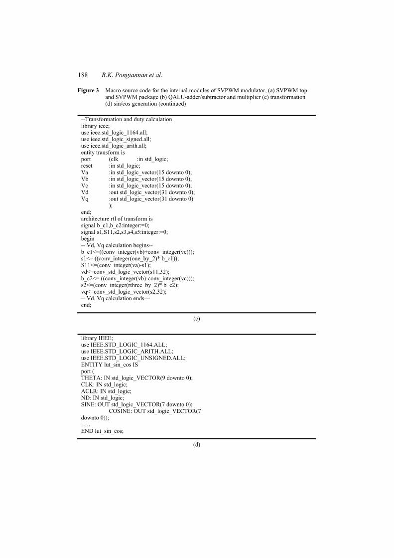
Figure 3 Macro source code for the internal modules of SVPWM modulator, (a) SVPWM top and SVPWM package (b) QALU-adder/subtractor and multiplier (c) transformation (d) sin/cos generation
entity svpwm_top is port (reset:in std_logic; Ts :in std_logic; clk :in std_logic; Vdc :in std_logic_vector(9 downto 0); Va :in std_logic_vector(7 downto 0); Vb :in std_logic_vector(7 downto 0); Vc :in std_logic_vector(7 downto 0); delT :integer;-- range should be 0<=delT<=t0/2 theta :in std_logic_vector(9 downto 0); S1,S3,S5: out std_logic; S4,S6,S2: out std_logic ); end;-- library ieee; use ieee.std_logic_1164.all; use ieee.std_logic_arith.all; use ieee.std_logic_signed.all; package svpwm_pkg is ----- for three phase sine generation -- FUNCTION R2B (M :REAL range -1.0 to +1.0 ; Y:INTEGER) RETURN std_logic_vector; FUNCTION B2R ( S : std_logic_vector) RETURN REAL; --QALU Functions -- FUNCTION qmul(a,b:std_logic_vector(7 downto 0)) return std_logic_vector; FUNCTION qasub(a,b:std_logic_vector(7 downto 0),mode:std_logic) return std_logic_vector; -- if mode => '0'=>add,'1'=>sub --- end; package body svpwm_pkg is ... end;
(a)

FPGA realisation of an area efficient SVPWM modulator 187
Figure 3 Macro source code for the internal modules of SVPWM modulator, (a) SVPWM top and SVPWM package (b) QALU-adder/subtractor and multiplier (c) transformation (d) sin/cos generation (continued)
(b)
188 R.K. Pongiannan et al.
Figure 3 Macro source code for the internal modules of SVPWM modulator, (a) SVPWM top and SVPWM package (b) QALU-adder/subtractor and multiplier (c) transformation (d) sin/cos generation (continued)
--Transformation and duty calculation library ieee; use ieee.std_logic_1164.all; use ieee.std_logic_signed.all; use ieee.std_logic_arith.all; entity transform is port (clk :in std_logic; reset :in std_logic; Va :in std_logic_vector(15 downto 0); Vb :in std_logic_vector(15 downto 0); Vc :in std_logic_vector(15 downto 0); Vd :out std_logic_vector(31 downto 0); Vq :out std_logic_vector(31 downto 0) ); end; architecture rtl of transform is signal b_c1,b_c2:integer:=0; signal s1,S11,s2,s3,s4,s5:integer:=0; begin -- Vd, Vq calculation begins-- b_c1<=((conv_integer(vb)+conv_integer(vc))); s1<= ((conv_integer(one_by_2)* b_c1)); S11<=(conv_integer(va)-s1); vd<=conv_std_logic_vector(s11,32); b_c2<= ((conv_integer(vb)-conv_integer(vc))); s2<=(conv_integer(rthree_by_2)* b_c2); vq<=conv_std_logic_vector(s2,32); -- Vd, Vq calculation ends--- end;
(c)
library IEEE; use IEEE.STD_LOGIC_1164.ALL; use IEEE.STD_LOGIC_ARITH.ALL; use IEEE.STD_LOGIC_UNSIGNED.ALL; ENTITY lut_sin_cos IS port ( THETA: IN std_logic_VECTOR(9 downto 0); CLK: IN std_logic; ACLR: IN std_logic; ND: IN std_logic; SINE: OUT std_logic_VECTOR(7 downto 0); COSINE: OUT std_logic_VECTOR(7 downto 0)); ….. END lut_sin_cos;
(d)

FPGA realisation of an area efficient SVPWM modulator 189
4 Simulation and experimental results
The proposed signal processing concept with the Q-format representation and the SVPWM modulator for power converter has been simulated using ModelSim 5.7 and implemented using Xilinx 9.1i. The Q-format data representation and the arithmetic operations of addition, subtraction and multiplication has been developed and simulated. The signal processing with Q-format has been implemented for the SVPWM pattern generation.
4.1 Simulation study
The simulation results for addition, subtraction and multiplication operation implemented using integer fixed and Q-format has been obtained for unsigned and signed data inputs. The SVPWM switch patterns for six sectors with different switching frequencies are obtained. The Q-format implementation has been validated with the simulation and implementation of an arithmetic operation (multiplication) and the corresponding implementation report and the results are shown in Tables 3 and 4, and Figure 4 respectively. The implementation summary of the SVPWM with 8/16-bit Q-format implementation is given in Tables 5 and 6 respectively. Table 3 Implementation report of fixed point integer arithmetic
Logic utilisation Used Available Utilisation
Number of four input LUTs 94 4,896 1% Logic distribution Number of occupied slices 50 2,448 2% Number of slices containing only related logic 50 50 100% Number of Slices containing unrelated logic 0 50 0% Total number of four input LUTs 96 4,896 1% Number of bonded IOBs 64 158 40% Number of MULT18X18SIOs 3 12 25% Total equivalent gate count for design 975
Table 4 Implementation report of Q-format arithmetic
Logic utilisation Used Available Utilisation
Number of four input LUTs 30 4,896 1% Logic distribution Number of occupied slices 16 2,448 1% Number of slices containing only related logic 16 16 100% Number of slices containing unrelated logic 0 16 0% Total number of four input LUTs 30 4,896 1% Number of bonded IOBs 64 158 40% Number of MULT18X18SIOs 3 12 25% Total equivalent gate count for design 348

190 R.K. Pongiannan et al.
Figure 4 Results of fixed point integer part and Q-format multiplication (see online version for colours)
Table 5 Implementation report of SVPWM with eight-bit WL with Q-format arithmetic
Modules Parameter
3/2 transformation
Sector find
Switch pattern QALU Duty
calculator SVPWM
Number of slices 128 55 362 42 352 734 Number of four input LUTs 256 211 708 76 667 1365
Number of IOs 146 61 91 26 93 37 Number of bonded IOBs 146 61 91 26 93 37
Table 6 Implementation report of SVPWM with 12-bits WL with Q-format arithmetic
Modules Parameter
3/2 transformation
Sector find
Switch pattern QALU Duty
calculator SVPWM
Number of slices 192 80 384 63 423 1013 Number of four input LUTs 266 224 1226 93 1335 2730
Number of IOs 154 65 103 38 109 49 Number of bonded IOBs 154 65 103 38 109 49
In multiplication of two unsigned data 0.25 and 0.75, the result is 0.1875. From the simulation shown in Figure 3, the result achieved using Q-format is 0.1875. For the same data, the answer achieved from integer fixed point format is 0D00H. The actual value evaluated by the digital controller is 0.203125 as per the procedure given in Appendix 1.
For example, 0.25*0.75 = 0.1875
• In Q-format, the result is 0.1875.
• In integer fixed point format, the result is 0.203125
The error is evaluated as:
( )0.1875 0.203125 0.015625 1.56% for one eight-bit multiplication operation− = − −

FPGA realisation of an area efficient SVPWM modulator 191
This procedure takes more number of clock cycles and utilises more resources in the FPGA.
The SVPWM patterns have been obtained for different switching frequencies (fz) and the result for 20 kHz is shown in Figures 5 to 6 respectively.
Tables 3 and 4 show the device utilisation summary of integer fixed point and Q-format implementation of the multiplication respectively. The results show that the Q-format implementation takes total gate count of 348 and integer fixed format implementation takes 975. The Q-format takes less chip resources and due to this feature, the speed of execution will also be increased. The error of a single multiplication operation with integer fixed point format is –1.56%. Therefore, the accuracy has been increased by Q-format when compared to integer fixed format. The Q-format based signal processing in FPGA reduces the IC resource utilisation with improved accuracy. The SVPWM patterns have been generated using the proposed signal processing with Q-format. The switching frequency is reprogrammable and can be set to the maximum value of 100 kHz in real time implementation, but due to switching frequency constraints in power devices a maximum of 20 kHz is used.
Figure 5 SVPWM waveforms in all six sectors for with fz = 20 kHz (Xilinx simulator) (see online version for colours)
Figure 6 SVPWM waveforms in all six sectors for with fz = 20 kHz (ModelSim simulator) (see online version for colours)
4.1.1 Performance comparison
For resource utilisation analysis, the internal modules of the SVPWM modulator is synthesised in Xilinx ISE 9.1i with XC3S400PQ208 FPGA having 8,064 equivalent LEs. The implementation report for eight-bit and 12-bit implementations is given in Tables 5 and 6 respectively. To highlight the area- and speed-efficiency, some comparative

192 R.K. Pongiannan et al.
investigations between the designed SVPWM IP-core and some reported examples are carried out. In Tzou and Hsu (1997), Chen and Joos (2002), and Zhou et al. (2004a), an FPGA-based SVPWM generator has been reported, where a host processor is used to carry out part of the SVPWM algorithm and remaining part is implemented in FPGA and also the data handles is in integer fixed point format. In Moreira et al. (2000), an FPGA-based SVPWM generator has been reported, where a total of 1,156 LEs was required with eight-bit reference inputs, and a maximum operating frequency is 7.12 MHz. The SVPWM reported in Chen and Joos (2002) and Zhou et al. (2004a), can be operated at higher frequencies, but takes large amount of hardware resources even with additional auxiliary controller. In Shu et al. (2007), 12-bit SVPWM is implemented EPIC12Q240C8 and the total area occupied by the design is 1,796 (15%) LEs. In the proposed 12-bit SVPWM using Q-format, the total utilisation is 1,013 (12.56%).
4.2 Experimental verification
The block diagram of the induction motor drive with FPGA based SVPWM controller is shown in Figure 7 and the photograph of the experimental setup is shown in Figure 8. The experiment has been carried out with the FPGA hardware Spartan XC3S400PQ208 from Xilinx Inc. The hardware setup consists of FPGA, induction motor, three phase bridge inverter with IGBTs, bridge rectifier to supply DC voltage, opto isolator and a pulse driver. The power module is three-phase voltage source inverter bridge with six power MOSFETs. The opto isolator IL260 provides the electrical isolation between the FPGA controller and power circuit. The MOSFET amplifier provides the amplified PWM signals to drive the gate of the power devices. The FPGA in the system can be operated with a maximum clock of 100 MHz, but the power devices will not respond to such high switching frequencies. Therefore, the simulation is carried out with the frequencies from low to high frequency in the order 100 kHz and in the real time experiments, the maximum switching frequency is about 20 kHz is used. In the experiments, the fundamental frequency has been varied from 0.3 Hz to 50 Hz and the switching frequency is varied from 1 kHz to 15 kHz and thus the PWM switching patterns are achieved. The results for PWM output in the different channels are obtained and the PWM patterns in the channels P1–P4, P2–P5 and P3–P6 are shown in Figures 9 to 12 respectively. The three phase inverter output wave forms with varying fundamental (f0) of 15 Hz to 50 Hz with 1.157 kHz to 12.28 kHz varying switching frequency (fz) is obtained. The result of the inverter output voltages, the line to line voltages URY, UYB and UBR for three phase is shown in Figures 13 to 18. The inverter output voltage with f0 = 50 Hz and fz = 1.157 kHz are shown in Figures 13 to 16. The Figures 17 and 18 shows the inverter output voltage with fundamental (f0) 15 Hz with 10.42 kHz switching frequency (fz) and with fundamental (f0) 30 Hz with 12.28 kHz switching frequency (fz) respectively. The inverter fed induction motor (0.25 hp/0.18 kW, three-phase, 415 V, 50 Hz) drive has been tested at no load with different frequencies.
From the simulation results, the Q-format takes less chip resources and also the result is accurate when compared to integer fixed format. In conventional FPGA implementations, the signal processing used is integer fixed point representation. The Q-format based signal processing in FPGA reduces the IC resource utilisation with improved accuracy. The experimental results for the FPGA output (PWM pulses) and the AC output waveform of the three phase inverter shows the feasibility of the practical implementation of the proposed SVPWM IP core for induction motor drive applications.

FPGA realisation of an area efficient SVPWM modulator 193
Table 7 Induction motor drive speed for different fundamental frequencies
S. no Fundamental frequency, f0 (Hz)
Calculated speed for four pole (RPM)
Measured speed (RPM)
1 0.15 4.5 4.0 2 0.3 9 8.0 3 1.0 30 28 4 3.0 90 87 5 10.0 300 296 6 15.0 450 445 7 30.0 900 885 8 50.0 1500 1493
Figure 7 Block diagram of the induction motor drive system with FPGA based SVPWM controller
Figure 8 Photograph of the experimental setup with induction motor (see online version for colours)
Uncontrolled bridge rectifier Filter circuit
Three-phase VSI bridge – power circuit
PC with JTAG
FPGA –SVPWM controller
Interfacing, isolation and amplification
3-ph IM
Induction motor FPGA
Power module
Driver circuit

194 R.K. Pongiannan et al.
Figure 9 SVPWM wave form in P1 and P4 with fz = 1.157 kHz (see online version for colours)
Figure 10 SVPWM wave form in P1and P4 with fz = 1.157 kHz with delay time in the pulses applied to the lower switch (see online version for colours)
Figure 11 SVPWM wave form in P2 and P5 with fz = 1.157 kHz (see online version for colours)
Pulse P1
Pulse P5

FPGA realisation of an area efficient SVPWM modulator 195
Figure 12 SVPWM wave form in P3 and P6 with fz = 1.157 kHz (see online version for colours)
Figure 13 Inverter output voltage: URY – line to line voltage, f0 = 50 Hz with fz =1.157 kHz (see online version for colours)
Figure14 Inverter output voltage: UYB – line to line voltage, f0 = 50 Hz with fz =1.157 kHz (see online version for colours)
50 V
/div
5 mS/div
50 V
/div
5 mS/div

196 R.K. Pongiannan et al.
Figure 15 Inverter output voltage: UBR – line to line voltage, f0 = 50 Hz with fz = 1.157 kHz (see online version for colours)
Figure 16 Inverter output voltage: URB and UYB – line to line voltage, f0 = 50 Hz with fz = 1.157 kHz (see online version for colours)
Figure 17 Inverter output voltage: URY and UYB – line to line voltage, f0 = 15 Hz with fz = 10.42 kHz (see online version for colours)
50 V
/div
20 mS/div
50 V
/div
5 mS/div
50 V
/div
20 mS/div

FPGA realisation of an area efficient SVPWM modulator 197
Figure 18 Inverter output voltage: UYB and UBR – line to line voltage, f0 = 30 Hz with fz = 12.28 kHz (see online version for colours)
5 Conclusions
To facilitate the digital implementation of the VLSI signal processing using Q-format representation of the data, the single chip FPGA implementation for SVPWM has been developed in this paper. By employing the new VLSI signal processing, the algorithm accuracy has been improved as well as the IC resource utilisation is tremendously reduced. Due to this superiority, the IP core designed on FPGA requires less resource and provides improved accuracy in single chip FPGA implementation compared to integer fixed point representation for signal processing. The efficient SVPWM IP core is implemented in a single FPGA and the experiments are carried out with a three-phase voltage source inverter for different operating frequencies. The induction motor drive speed with different operating frequencies is verified. The proposed VLSI signal processing with Q-format data representation can be used for software application such as DSP and microcontrollers technologies to generate the accurate PWM pattern in real time. Moreover, the developed SVPWM IP core with proposed signal processing method is more suitable for single chip FPGA and SOC implementations of power electronic converter control algorithms and motor control systems.
References Bateman, A. and Yates, W. (1990) Digital Signal Processing Design, A.H. Wheeler & Co., Ltd.,
Wiley Publishing Co., First Indian reprint. Chen, S. and Joos, G. (2002) ‘Symmetrical SVPWM pattern generator using field programmable
gate array implementation’, IEEE Proc. of APEC ’02, USA, Vol. 2, pp.1004–1010. Du, Z. and Wang, X. (2007) ‘SVPWM speed governing system of induction motor based on DSP’,
IEEE Proc. of EUROCON 2007, Warsaw, pp.45–49. Fan, Y., Xing, Y. and Hu, Y. (2004) ‘A fast algorithm for SVPWM in three phase power factor
correction application’, IEEE Proc. of PESC’04, Germany, pp.976–979.
50 V
/div
10 mS/div
Displacement between two voltage waves

198 R.K. Pongiannan et al.
Finch, J.W. and Giaouris, D. (2008) ‘Controlled AC electric drives’, IEEE Trans. on Industry Applications, Vol. 55, No. 2, pp.481–491.
Flaabjerg, F., Consoli, A., Ferraria, J.A. and Van Wyk, J.D. (2005) ‘The future of power processing and conversion’, IEEE Trans. on Industry Applications, Vol. 41, No. 1, pp.3–8.
Hao, M., Yunping, L. and Huiming, C. (2004) ‘A simplified algorithm for space vector modulation of three-phase voltage source PWM rectifier’, IEEE Proc. of Power Electronic Specialist Conference-PESC’04, Germany, pp.3665–3670.
Holtz, J. (1992) ‘Pulse width modulation – a survey’, IEEE Trans. on Industry Electronics, Vol. 39, No. 5, pp.410–420.
Holtz, J. (1994) ‘Pulse width modulation for electronic power conversion’, Proceeding of the IEEE, Vol. 82, No. 8, pp.1194–1214.
IEEE Standards for Floating Point Representation – IEEE 754, online, available at http:// www.ieee.org.
Markovic, D.M. (2006) ‘A power/area optimal approach to VLSI signal processing’, PhD dissertation, May, Electrical Engineering and Computer Sciences, University of California at Berkeley.
Moreira, C.S., Freire, R.C.S., Melcher, E.U.K., Deep, G.S., Catunda, S.Y.C. and Alves, R.N.C. (2000) ‘FPGA based SVPWM trigger generator for 3-phase voltage source inverter’, IEEE Proc. of Instr. Meas. Technol. Conf., pp.174–178.
Narayanan, G., Krishnamurthy, H.K., Zhao, D. and Ayyanar, R. (2006) ‘Advanced bus clamping PWM techniques based on space vector approach’, IEEE Trans. on Power Electronics, Vol. 21, No. 4, pp.974–94.
Oberstar, E.L. (2007) Fixed Point Representation and Fractional Math, Revision 1.2, August, Oberstar Consulting, online, available at http://superkits.net/whitepapers/pp1-18.
Parhami, B. (2005) Computer Architecture, Oxford University Press, New York. Parkhi, V., Shilaskar, S., Tirmare, M. and Jog, M. (2008) ‘FPGA implementation of PWM control
technique for three phase induction motor drive’, IEEE Proc. of ICETET-2008, pp.996–1001. Pongiannan, R.K. and Yadaiah, N. (2006) ‘FPGA based space vector PWM Control IC for three
phase induction motor drive’, IEEE Proc. of Industrial Technology ICIT‘06, India, pp.2061–2066.
Pongiannan, R.K. and Yadaiah, N. (2007) ‘Single chip FPGA based space vector PWM controller for three phase induction motor drive’, Journal of Computer Science, Vol. 1, No. 6, pp.428–437.
Pongiannan, R.K. and Yadaiah, N. (2008a) ‘A novel VLSI architecture for single chip space vector PWM modulator used in three phase inverters’, National Journal of Technology, PSG College of Technology, Vol. 1, No. 4, pp.61–74.
Pongiannan, R.K. and Yadaiah, N. (2008b) ‘FPGA applications in DC-AC converters: a single chip implementation of SPWM and SVPWM modulators’, Journal of Computer Science, Vol. 2, No. 3, pp.620–633.
Shu, Z., Tang, J., Guo, Y. and Lian, J. (2007) ‘An efficient SVPWM algorithm with low computational overhead for three-phase inverters’, IEEE Trans. on Power Electronics, Vol. 22 No. 5, pp.1797–1805.
Tunyasrirut, S., Srilad, S. and Suksri, T. (2008) ‘Comparison power quality of the voltage source inverter type SVPWM and SPWM technique for induction motor drive’, Proc. of SICE Annual Conf. 2008, The University Electro-Communications, Japan, pp.241–246.
Tzou, Y.Y. and Hsu, H.J. (1997) ‘FPGA realization of space vector PWM control IC for three phase PWM inverters’, IEEE Trans. on Power Electronics, Vol. 12 No. 6, pp.953–963.
Xilinx Inc. (2006) Foundation Series ISE 9.li User Guide. Xilinx, Inc Cordic v3.0 (2004) Datasheet DS249, May, online, available at http://www.xilinx.com. Yang, G., Zhao, P. and Zhou, Z. (2008) ‘The design of SVPWM IP core based on FPGA’, IEEE
Proc .of ICESS-2008, pp.191–196.
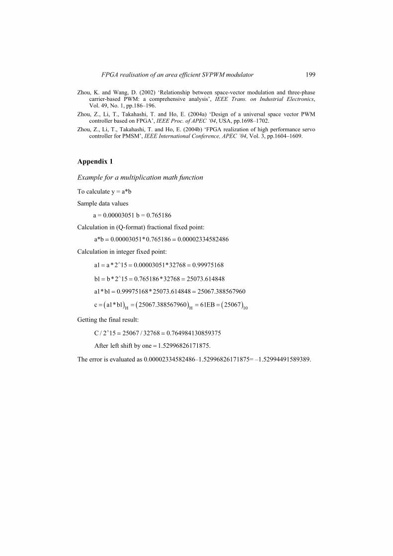
FPGA realisation of an area efficient SVPWM modulator 199
Zhou, K. and Wang, D. (2002) ‘Relationship between space-vector modulation and three-phase carrier-based PWM: a comprehensive analysis’, IEEE Trans. on Industrial Electronics, Vol. 49, No. 1, pp.186–196.
Zhou, Z., Li, T., Takahashi, T. and Ho, E. (2004a) ‘Design of a universal space vector PWM controller based on FPGA’, IEEE Proc. of APEC ‘04, USA, pp.1698–1702.
Zhou, Z., Li, T., Takahashi, T. and Ho, E. (2004b) ‘FPGA realization of high performance servo controller for PMSM’, IEEE International Conference, APEC ’04, Vol. 3, pp.1604–1609.
Appendix 1
Example for a multiplication math function
To calculate y = a*b
Sample data values
a = 0.00003051 b = 0.765186
Calculation in (Q-format) fractional fixed point:
a*b 0.00003051*0.765186 0.00002334582486= =
Calculation in integer fixed point:
a1 a *2 15 0.00003051*32768 0.99975168∧= = =
b1 b*2 15 0.765186*32768 25073.614848∧= = =
a1*b1 0.99975168*25073.614848 25067.388567960= =
( ) ( ) ( )H H 10c a1*b1 25067.388567960 61EB 25067= = = =
Getting the final result:
C / 2 15 25067 / 32768 0.764984130859375∧ = =
After left shift by one 1.52996826171875.=
The error is evaluated as 0.00002334582486–1.52996826171875= –1.52994491589389.
FPGA Based Three Phase Sinusoidal PWM VVVF Controller
R. K. Pongiannan1, Member- IEEE, P. Selvabharathi2 N. Yadaiah, Sr. Member-IEEE 1Dept. of EIE / 2Dept. of EEE Dept. of Electrical and Electronics Engg. Bannari Amman Institute of Technology JNTUH College of Engineering,
Sathyamangalam, TN. India Hyderabad,AP., India [email protected], [email protected],. [email protected]
Abstract
The SPWM control in a single FPGA has been developed and implemented. The SPWM IP core is designed using VHDL and a single FPGA, SPARTAN XC3S400PQ208 from Xilinx Inc. The simulations are carried out using ModelSim 5.7 and the implementation is carried out using Xilinx foundation series 9.1i. The PWM patterns have been achieved for different switching and fundamental frequencies. The output fundamental can be varied from 0.1 Hz to 1.5 kHz and the PWM switching can be set from 0.2 Hz to 100 MHz. The simulation and experimental results are presented.
Keywords : Sinusoidal PWM, FPGA.
I. INTRODUCTION
In the industrial applications, many three-phase loads require a supply of Variable Voltage Variable Frequency (VVVF) including fast and high-efficient electronic control. Predominant applications are in variable speed AC drives and power conditioning systems. The conversion of DC power to three-phase AC power is exclusively performed in the switched mode. The temporary connections to the power semiconductor switches at high repetition rates between the two DC terminals and the three phases of the AC drive motor is performed. The actual power flow in each motor phase is controlled by the on/off ratio, or duty-cycle, of the respective switches. The desired sinusoidal waveform of the currents is achieved by varying the duty-cycles sinusoidally with time, employing techniques of Pulse Width Modulation (PWM) [1-2]. The PWM strategy plays an important role in the minimization of harmonics and switching losses in these converters, especially in three-phase applications. In the past two decades, various PWM strategies, control schemes, and realization techniques have been developed. Many PWM schemes have been developed by many researchers to obtain the desired performance or to overcome the existing limitations such as DC bus utilization, linear operating range, high harmonic contents in the output, accuracy and speed in the digital PWM control. The different types of PWM control schemes are carrier based PWM also called Sinusoidal PWM (SPWM), Space Vector PWM (SVPWM), Selected Harmonic Injection PWM (SHIPWM) and Selected Harmonic Elimination PWM (SHEPWM) [1-2].
In the field of digital control in electrical systems, advanced microprocessors and Programmable Logic Devices (PLDs) are playing a critical role. Due to the higher gate densities and lower cost, FPGAs can target a large market of Application Specific Standard Products (ASSPs). Field Programmable Gate Array (FPGA) vendors are offering the software and hardware resources and Computer Aided Design (CAD) tools for their devices [3-5]. The algorithm is developed using HDL and the detailed tutorial of Very High Speed Integrated Circuit (VHSIC) Hardware Description Language (VHDL) with design examples are given in [6]. This method is as flexible as any software solution. Another important advantage of VHDL is that it is technology independent. The real time implementation of a PWM control scheme requires high performance digital controllers such as Digital Signal Processor (DSP), FPGA and combination of these. During 1980s, the low performance microprocessors were used [7]. In late 1990s, the DSPs were used for PE converter control [8]. DSPs providing the sequentially executable software solution and FPGA provide the concurrently executable hardware solution. Each device is having specific merits and demerits such as speed, input/output (I/O) capabilities, and memory space/ chip resources to store the application software and data size in signal processing. Since, FPGAs are executing the control statements concurrently, they offer the high speed computation in real time. Therefore, FPGA has been extensively used in many PEC control like DC-DC converters, matrix converters , resonant converters, converters with power factor correction, AC-DC converters [4]. In three-phase DC-AC converter (Inverters) control using SPWM [9-11], SVPWM [12-15], are reported. The host processors interfaced with FPGA to generate PWM are presented in [12-13]. The single chip FPGA based PWM controls using holistic modelling approach, Xilinx System Generator (XSG) based design, and modifying the PWM algorithm suitable for FPGA implementation are developed [14-15] and the various types electric drive control are presented in [4]. The feature of dynamic reconfiguration i.e. two or more control structure can be programmed in a single FPGA and the control can be changed between them, without shutting down the system is reported in [16].
34978-1-61284-379-7/11$26.00 c©2011 IEEE

The limitations in the existing FPGA based PWM control implementations are the need of a co-processor to compute the algorithms, operational speed and more utilization of FPGA resources. This paper presents the design and implementation of FPGA based efficient SPWM control through single FPGA. The paper is organized as follows: section II describes the principle of SPWM, Section III presents the FPGA implementation VLSI architecture for SPWM controller, and Section IV deals with the implementation of the SPWM controller. Finally conclusions are summarized in section V.
II. PRINCIPLE OF SPWM
The most widely used method of PWM is carrier based. Sinusoidal modulation is based on triangular carrier signal and level comparison between them produces the PWM gating signal. The modulating and triangular reference signal is shown in Fig. 1 and the procedure to generate the gating signals are shown in Fig. 2. [1-2, 9]. Amplitude modulation index is given by
cr
ma u
uM
ˆ
ˆ= (1)
Frequency modulation index
m
crf f
fM = (2)
where fcr is the frequency of carrier and fm is the frequency of modulating wave.
The time for vertex sampling point and the nadir sampling is t1
and t2 respectively. The sampling points, t1 and t2 are shown in Fig. 2 and they are calculated using the following relations [85]:
kT
t t
21 = (when k = 0, 2, 4, 6, …)
kT
t t
22 = (when k = 1, 3, 5, 7, …) (3)
tpu is the width of SPWM pulses, which can be expressed as
( ) 2121 sin42
sin4
sinsin2
12
tMTT
tMT
ttMT
t ttttpu ωωωω ++=⎥⎦
⎤⎢⎣⎡
++= (4)
where Ma= Uc/Ur is the modulation index,
Uc is the maximum value of the sine wave. Tt represents the period of the triangular carrier, and ω is the angular frequency of the sine wave.
III. FPGA IMPLEMENTATION VLSI ARCHITECTURE FOR SPWM CONTROLLER
The FPGA implementation of SPWM controller through FPGA is shown in Fig 3.. The single chip SPWM controller is developed using VHDL [6]. The designed VLSI Architecture for SPWM controller is implemented in a reprogrammable XC3S400PQ208 FPGA. The internal modules of the architecture are Q –Format Arithmetic Logic Unit (QALU), clock divider, frequency selector, sin generator, PWM controller and dead time module. The QALU performs all arithmetic and logic functions in Q-Format representation [15-16]. In the FPGA implementation the QALU is constructed as generic library function. Each module is described with VHDL, compiled and simulated in the environment of Xilinx.
A. Q –Format Arithmetic Logic Unit (QALU) The QALU designed performs the data representation, arithmetic and logic operations in the SPWM algorithm using Q-Format. The QALU in FPGA is implemented as generic library function. The VHDL code for QALU arithmetic operations like addition and mltiplication has been developed. This ALU can be used as core for designing FPGA based dedicated processors for inverter and motor control applications [4,16].
B. Clock Divider
In the FPGA development board, a common clock of 10 MHz is provided by the oscillator. But, the operation speed or clock for each module in the design is varying. Therefore, a Clock divider is used to generate the clock for sine wave generator, triangular wave generator comparator and PWM modules. Foclk is the fo control clock. To get different frequency ratios the clock divider is needed to generate 50%
Fig. 1. Modulating and Carrier waves
0
u umA Bm
u Cm u
muu cr ω t
ucr – Carrier wave um – Modulating wave
ucr
Ur
t2
t
t
t
TsTs
Uc sin ωt
Fig. 2. Asymmetric regular sampled PWM
t1
Ts Ts/2
2011 1st International Conference on Electrical Energy Systems 35
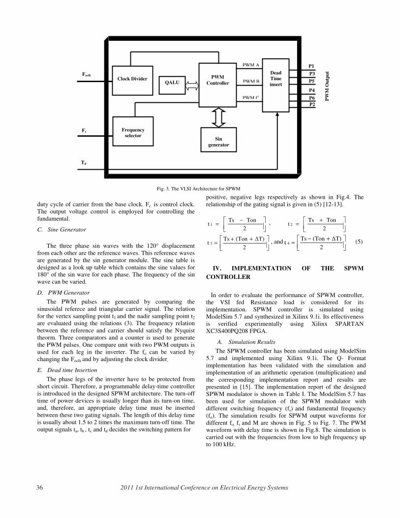
duty cycle of carrier from the base clock. Fc is control clock. The output voltage control is employed for controlling the fundamental.
C. Sine Generator
The three phase sin waves with the 120° displacement from each other are the reference waves. This reference waves are generated by the sin generator module. The sine table is designed as a look up table which contains the sine values for 180° of the sin wave for each phase. The frequency of the sin wave can be varied.
D. PWM Generator
The PWM pulses are generated by comparing the sinusoidal referece and triangular carrier signal. The relation for the vertex sampling point t1 and the nadir sampling point t2 are evaluated using the relations (3). The frequency relation between the reference and carrier should satisfy the Nyquist theorm. Three comparators and a counter is used to generate the PWM pulses. One compare unit with two PWM outputs is used for each leg in the inverter. The fo can be varied by changing the Foclk and by adjusting the clock divider.
E. Dead time Insertion
The phase legs of the inverter have to be protected from short circuit. Therefore, a programmable delay-time controller is introduced in the designed SPWM architecture. The turn-off time of power devices is usually longer than its turn-on time, and, therefore, an appropriate delay time must be inserted between these two gating signals. The length of this delay time is usually about 1.5 to 2 times the maximum turn-off time. The output signals ta, tb , tc and td decides the switching pattern for
positive, negative legs respectively as shown in Fig.4. The relationship of the gating signal is given in (5) [12-13].
⎥⎦⎤
⎢⎣⎡ −
=2
Ton Tst 1 ,
⎥⎦⎤
⎢⎣⎡ +
=2
Ton Tst 2
⎥⎦⎤
⎢⎣⎡ ++
=2
ΔT)(TonTst 3 , and ⎥⎦
⎤⎢⎣⎡ +−
=2
ΔT)(TonTst 4 (5)
IV. IMPLEMENTATION OF THE SPWM CONTROLLER
In order to evaluate the performance of SPWM controller, the VSI fed Resistance load is considered for its implementation. SPWM controller is simulated using ModelSim 5.7 and synthesized in Xilinx 9.1i. Its effectiveness is verified experimentally using Xilinx SPARTAN XC3S400PQ208 FPGA.
A. Simulation Results
The SPWM controller has been simulated using ModelSim 5.7 and implemented using Xilinx 9.1i. The Q- Format implementation has been validated with the simulation and implementation of an arithmetic operation (multiplication) and the corresponding implementation report and results are presented in [15]. The implementation report of the designed SPWM modulator is shown in Table I. The ModelSim 5.7 has been used for simulation of the SPWM modulator with different switching frequency (fs) and fundamental frequency (fo). The simulation results for SPWM output waveforms for different fo, fs and M are shown in Fig. 5 to Fig. 7. The PWM waveform with delay time is shown in Fig.8. The simulation is carried out with the frequencies from low to high frequency up to 100 kHz.
P5
Dead Time insert
Clock Divider
PWM
Controller QALU
Fc
Foclk
Fig. 3. The VLSI Architecture for SPWM
Frequency
selector Sin
generator
PWM A
PWM B
PWM C
P1
P3
P4
P6
Td
P2
PW
M O
utpu
t
36 2011 1st International Conference on Electrical Energy Systems

TABLE -I. IMPLEMENTATION REPORT OF SPWM
Logic Utilization Used Available Utilization
Number of Slice Flip Flops 341 7,168 4%
Number of 4 input LUTs 1,102 7,168 15%
Number of occupied Slices 737 3,584 20%
No.of Slices containing related logic
737 737 100%
Number of bonded IOBs 13 141 9%
Number of MULT18X18s 1 16 6%
Total equ. gate count for design
15,587
Fig. 6. Three Phase SPWM waveforms with fs = 20 kHz, fo = 50 Hz, and M=0.65 ( Expanded scale)
Fig. 5. Three Phase SPWM waveforms with fs = 20 kHz, fo = 50 Hz, and M=0.65
Analog form of Sine signal
Fig. 4. PWM waveforms with delay time
Ton Toff
Ts
Ton
ΔT
Ts
t
t
tatb
tc
td ΔT
Ts Ts
P1
P4
2011 1st International Conference on Electrical Energy Systems 37

B. Experimental Verification
The experimentation has been carried out with the FPGA hardware SPARTAN XC3S400PQ208 from Xilinx. Inc. The hardware setup consists of FPGA, three phase VSI with IRFP460 MOSFETs, bridge rectifier to supply DC voltage, opto isolator, pulse driver and load. The experimental setup is shown in Fig. 8. The power module is 3- phase VSI Bridge with 6 power MOSFETs. The opto isolator IL260 provides the electrical isolation between the FPGA controller and power circuit. The MOSFET amplifier provides the amplified PWM signals to drive the gate of the power devices. The FPGA in the system can operate with a maximum clock of 50 MHz, but the power devices will not respond to such high switching frequencies. Therefore the experiments are conducted with a maximum f0 of 20 kHz.
Fig. 7. Three Phase SPWM waveforms with, fs = 10 kHz, fo = 30 Hz, and M=0.75
Fig. 9. Experimental setup of SPWM controller fed three induction motor
FPGA
Pulse driver Amp OPTO isolation
Power Module
Fig. 8. Three Phase SPWM waveforms with fs = 20 kHz, fo = 50 Hz, and M=0.65 showing the dead time
Dead time
38 2011 1st International Conference on Electrical Energy Systems

The real time PWM gating signals in 6 channels are obtained and the the SPWM wave form in P5 with fs=10 kHz and f0 = 50 Hz is shown in Fig. 10. The inverter output for different switching and fundamental frequency was verified. The Line to Line voltage (R-Y) for three phase star connected R load: fs=10 kHz, f0 = 50 Hz, and M=0.65 is shown in Fig.11. The simulation and experimental results are presented for different settings frequencies of the SPWM controller.
V. CONCLUSION
The SPWM control in a single FPGA has been developed and implemented. The SPWM IP core is designed using VHDL and a single FPGA, SPARTAN XC3S400PQ208 from Xilinx Inc. The simulations are carried out using ModelSim 5.7 and the implementation is carried out using Xilinx foundation series 9.1i. The functionality of the SPWM IP core is verified for different switching and fundamental frequencies. The PWM patterns have been achieved for
different fs with fo of 50 Hz. The output fo can be varied from 0.1 Hz to 1.5 kHz and the PWM switching can be set from 0.2 Hz to 100 MHz. The experimental results are obtained for the fs up to 20 kHz with a varying fundamental from 0.3 Hz to 60 Hz. The developed SPWM IP core can be used as modulator for AC drives, UPS system and power conditioning systems. Also this SPWM controller can be used to provide a single FPGA implementation for multilevel and multi phase drives.
REFERENCES
[1] B. K. Bose, “Modern power electronics and ac drives,” Upper Saddle River, NJ: Prentice-Hall, 2002.
[2] J. Holtz, “Pulse Width Modulation for Electronic Power Conversion,” Proceeding of the IEEE, vol. 82, no. 8, 1994, pp. 1194 – 1214.
[3] J. J. R. Odriguez-Andina, M. J. Moure, and M. D. Valdes, “Features, design tools, and application domains of FPGAs” IEEE Trans. Ind. Electron., vol. 54, no. 4, 2007, pp. 1810-1823.
[4] R. K. Pongiannan, S. Paramasivam, and N. Yadaiah, “FPGA applications in power electronic converter and electric drive control- A review,” Int. Journal of Electrical Engg. and Embedded Systems, vol. 2, no. 1, 2010, pp. 29-58.
[5] Xilinx Corporation “Xilinx Spartan-3E FPGA family: Complete data sheet,” 2007. [Online]. Available: http://www.xilinx.com.
[6] Douglas. L. Perry, VHDL: Programming by examples. New York: McGraw-Hill, 2002.
[7] S. R. Bowes and M. J. Mount, “Microprocessor control of PWM inverters,” in Proc. IEE-Elec. Power Appl., vol. 128, no. 6, 1981, pp. 293-305.
[8] D. Hadiouche, L. Baghli, and A. Rezzoug, “Space vector PWM techniques for dual three-phase ac machine: analysis, performance evaluation and DSP implementation,” IEEE Trans. Ind. Appl, vol. 42, no. 4, 2006, pp. 1112-1122.
[9] Z. Zhou, G. Yang, and Tiecai Li, “Design and implementation of FPGA based 3- phase Sinusoidal PWM VVVF controller,” in Proc. IEEE- APEC’04, 2004, vol. 3, pp. 1703-1708.
[10] Y. Yuan, G. Yong, and C. Lijie, “Design and test of novel programmable digital three phases SPWM chip,” in Proc. IEEE- IPEMC ‘06, Shanghai, 2006, pp. 1-3.
[11] F. Vargas, M. J. Meco, J. R. Heredia and A. Ruiz, “Highly efficient PWM strategy over FPGA,” IET- Electron. Letters, vol. 44, no. 24, 2008, pp. 1396-1397.
[12] Y. Y. Tzou and H. J. Hsu, “FPGA realization of space vector PWM control IC for three phase PWM inverters,” IEEE Trans. Power Electron., vol. 12, no. 6, 1997, pp. 953-963.
[13] R. K. Pongiannan and N. Yadaiah, “FPGA based Space Vector PWM control IC for three phase induction motor drive,” in Proc. IEEE- ICIT 2006, pp. 2061-2066.
[14] Z. Shu, J. Tang, Y. Guo, and J. Lian, “An efficient SVPWM algorithm with low computational overhead for 3-phase inverters,” IEEE Trans. Power Electron., vol. 22, no. 5, 2007, pp. 1797-1805.
[15] R. K. Pongiannan, S. Paramasivam, and N. Yadaiah, “FPGA Realization of an area efficient SVPWM modulator for three phase induction motor drive,” Int. Journal of Power Electronics, Inderscience publishers, vol. 2, no. 2, 2010, pp. 176-199.
[16] R. K. Pongiannan, S. Paramasivam, and N. Yadaiah, “Dynamically reconfigurable PWM controller for three phase voltage source inverters,” IEEE Trans. on Power Electron. 2010. (In Press).
Fig. 10. SPWM wave form in P5 with fs=10 kHz and f0 = 50 Hz
500 ms /div
Fig. 11. The Line to Line voltage (R-Y) for three phase star connected R load: fs=10 kHz, f0 = 50 Hz, and M=0.65
Vol
tage
25
V/d
iv
Time 5 ms/div
2011 1st International Conference on Electrical Energy Systems 39