
Dynamic Self controllable Surfing for Differential on … Self controllable Surfing for Differential...
12
Dynamic Self controllable Surfing for Differential on-chip wave- pipelined serial interconnect BHASKAR. M, SRINIVAS GANTASALA, VENKATARAMANI. B Department of Electronics and Communication Engineering National Institute of Technology, Tiruchirappalli – 620015, INDIA [email protected], [email protected],[email protected] Abstract: - In the literature, surfing technique has been proposed for differential wave-pipelined serial interconnects with uniform repeaters (UR) and non-uniform repeaters (NUR) to increase the data transfer rate. In this paper, a new surfing circuit called „Dynamic self controllable inverter pair‟ is proposed for differential wave-pipelined serial interconnects with UR and NUR to increase the data transfer rate further. The method of logical effort is used for the design of surfing circuits both UR and NUR. To evaluate the efficiency of these techniques, 40 mm metal 4 interconnects using the proposed surfing techniques are implemented along with transmitter, receiver and delay locked loop(DLL) in UMC 180nm technology and their performances are studied through post layout simulations. From this study, it is observed that the proposed surfing technique using UR and NUR achieve 3.53 times and 3.76 times higher data transfer rates respectively compared to the single ended scheme. The proposed scheme using UR and NUR has 1.18 times and 1.25 times higher data transfer rates respectively compared to differential scheme. Key-Words: - Controllable inverter pair, Differential interconnect, Method of logical effort, Repeater insertion, Self controllable, Serial link, Surfing, Wave-pipelining 1 Introduction As the CMOS technology scales down, transistor sizes get reduced and this in turn increases the speed of the logic blocks [1]. The interconnects between the transistors, referred to as local interconnects, become shorter as technology scales down. However, interconnects used for routing signals between logic blocks, known as global interconnects, do not scale in length from one technology to another [2] and they limit the maximum data rate for on-chip communication. In order to achieve high data transfer rates in circuits using deep submicron technologies, the delay through the global interconnects needs to be reduced. For this purpose techniques such as repeater insertion [3], wire sizing [4], low swing signaling [5] and pulsed wave interconnects [9&10] have been proposed in literature. However, even with these techniques, the time required to transmit data across chip may be several clock periods or handshake cycles. An overview of the techniques used for interconnects in SoC design is presented next. Delay of interconnect is reported to be proportional to the square of length in [1]. Repeater insertion technique proposed in [3] makes the delay of RC interconnect line to be a linear function of length. The expressions for obtaining the optimum number of repeaters and their size for minimizing the delay of RC interconnects have been reported in [3]. For interconnect modeled as an RC network, width is considered as a design parameter and it is shown that the repeater insertion outperforms the wire sizing [4]. It is reported in [6] that the delay can be decreased by maximizing the line inductance particularly in low resistance materials with fast signal transitions. In [7], it is shown that the delay of on-chip interconnect obtained using RLC model is less compared to that using RC line model. However, the repeater insertion technique results in larger area, higher complexity in placement and routing and higher power dissipation. To overcome this, the repeater-less interconnect is proposed in [8]. It uses phase shift keying signaling scheme. This maximizes the inductive behavior and achieves almost near speed of light latency in silicon dioxide with high data rate on-chip interconnects. The pulsed wave interconnect is proposed for global interconnects in SoC applications in [9&10], where sharp current pulses are used to maximize the inductive behaviour. The pulsed current-mode signaling scheme is proposed in [10] for near speed of light on-chip communication. This uses output multiplexing scheme at the transmitter. As it requires a driver for each input to be multiplexed, it results in more area and power dissipation. To WSEAS TRANSACTIONS on CIRCUITS and SYSTEMS Bhaskar M., Srinivas Gantasala, Venkataramani B. E-ISSN: 2224-266X 117 Volume 13, 2014
Transcript of Dynamic Self controllable Surfing for Differential on … Self controllable Surfing for Differential...

Dynamic Self controllable Surfing for Differential on-chip wave-
pipelined serial interconnect
BHASKAR. M, SRINIVAS GANTASALA, VENKATARAMANI. B
Department of Electronics and Communication Engineering
National Institute of Technology, Tiruchirappalli – 620015, INDIA
[email protected], [email protected],[email protected]
Abstract: - In the literature, surfing technique has been proposed for differential wave-pipelined serial
interconnects with uniform repeaters (UR) and non-uniform repeaters (NUR) to increase the data transfer rate.
In this paper, a new surfing circuit called „Dynamic self controllable inverter pair‟ is proposed for differential
wave-pipelined serial interconnects with UR and NUR to increase the data transfer rate further. The method of
logical effort is used for the design of surfing circuits both UR and NUR. To evaluate the efficiency of these
techniques, 40 mm metal 4 interconnects using the proposed surfing techniques are implemented along with
transmitter, receiver and delay locked loop(DLL) in UMC 180nm technology and their performances are
studied through post layout simulations. From this study, it is observed that the proposed surfing technique
using UR and NUR achieve 3.53 times and 3.76 times higher data transfer rates respectively compared to the
single ended scheme. The proposed scheme using UR and NUR has 1.18 times and 1.25 times higher data
transfer rates respectively compared to differential scheme.
Key-Words: - Controllable inverter pair, Differential interconnect, Method of logical effort, Repeater
insertion, Self controllable, Serial link, Surfing, Wave-pipelining
1 Introduction As the CMOS technology scales down, transistor
sizes get reduced and this in turn increases the speed
of the logic blocks [1]. The interconnects between
the transistors, referred to as local interconnects,
become shorter as technology scales down.
However, interconnects used for routing signals
between logic blocks, known as global
interconnects, do not scale in length from one
technology to another [2] and they limit the
maximum data rate for on-chip communication. In
order to achieve high data transfer rates in circuits
using deep submicron technologies, the delay
through the global interconnects needs to be
reduced. For this purpose techniques such as
repeater insertion [3], wire sizing [4], low swing
signaling [5] and pulsed wave interconnects [9&10]
have been proposed in literature. However, even
with these techniques, the time required to transmit
data across chip may be several clock periods or
handshake cycles.
An overview of the techniques used for
interconnects in SoC design is presented next. Delay
of interconnect is reported to be proportional to the
square of length in [1]. Repeater insertion technique
proposed in [3] makes the delay of RC interconnect
line to be a linear function of length. The
expressions for obtaining the optimum number of
repeaters and their size for minimizing the delay of
RC interconnects have been reported in [3]. For
interconnect modeled as an RC network, width is
considered as a design parameter and it is shown
that the repeater insertion outperforms the wire
sizing [4]. It is reported in [6] that the delay can be
decreased by maximizing the line inductance
particularly in low resistance materials with fast
signal transitions. In [7], it is shown that the delay of
on-chip interconnect obtained using RLC model is
less compared to that using RC line model.
However, the repeater insertion technique results in
larger area, higher complexity in placement and
routing and higher power dissipation. To overcome
this, the repeater-less interconnect is proposed in
[8]. It uses phase shift keying signaling scheme.
This maximizes the inductive behavior and achieves
almost near speed of light latency in silicon dioxide
with high data rate on-chip interconnects.
The pulsed wave interconnect is proposed for
global interconnects in SoC applications in [9&10],
where sharp current pulses are used to maximize the
inductive behaviour. The pulsed current-mode
signaling scheme is proposed in [10] for near speed
of light on-chip communication. This uses output
multiplexing scheme at the transmitter. As it
requires a driver for each input to be multiplexed, it
results in more area and power dissipation. To
WSEAS TRANSACTIONS on CIRCUITS and SYSTEMS Bhaskar M., Srinivas Gantasala, Venkataramani B.
E-ISSN: 2224-266X 117 Volume 13, 2014

overcome this, the input multiplexed voltage mode
transmitter using pseudo NMOS logic is proposed in
[11] and it requires only one driver for all the inputs.
However, this architecture uses ratioed logic and
sensing logic zero level at higher frequencies
becomes difficult.
For single ended serial interconnect, an alternate
technique known as wave-pipelining is applied to
conventional repeater insertion technique to replace
the global clocks with local clocks in [12]. Wave-
pipelining enables multiple data waves to propagate
through uniformly buffered global interconnect
allowing to transmit data at a higher rate. However,
the data sent through wave-pipelined interconnects
are not reliable. To overcome this problem, surfing
technique is proposed in [13] for single ended
interconnect. In this technique, a control signal
denoted as 'req' is transmitted in a separate line
along with each buffered wave-pipelined
interconnect segment. This generates the surfing
signal 'fast' that controls the propagation delay of
each segment. When 'fast' is true, the delay of the
buffer in the particular interconnect segment
becomes lesser than the normal value. The circuit
used in [13] to generate signal 'fast' from 'req' needs
a setup timing constraint of about one fourth of the
clock period. The reliability of data transmitted is
ensured by the 'req' signal but reliability of the
transmission of 'req' is not ensured.
In [14], a differential wave-pipelined serial
interconnect is proposed to overcome the constraints
in single ended scheme. In this technique, the
complementary signal path is used to surf the true
signal path and vice versa. A separate line is not
required to propagate the control signal. It
eliminates the setup time constraint and the data
reliability is ensured both for true and complement
signals. The surfing scheme proposed in [14] is
capable of surfing only one signal path (either true
or complementary) at a time i.e. when the
complementary signal is delayed with respect to the
true signal, the surfing signals generated speeds up
only the complementary signal path and vice versa.
In [15], for differential wave-pipelined
interconnects, a new surfing technique which
generates the surfing signals during the overlapping
period of the true and complementary paths is
proposed both for uniform repeater (UR) and non
uniform repeater (NUR) insertion schemes. This
surfs both the true and complement lines at the same
time till they are exactly complement to each other.
The control signals required for surfing the true and
complementary paths are generated using separate
control circuits. Thus it provides a higher data rate
through the differential serial interconnect as
compared to [14].
In [13, 14 & 15], additional control circuitry is
used in order to generate the control signals for
surfing the true and complementary data paths. The
controllable inverter pair along with its control
circuitry is used at the end of each wave pipe-lined
segment. But nevertheless, the control circuit uses
pseudo NMOS based circuit which has higher static
power dissipation.
Therefore in order to avoid the complexity of
additional control circuit, a self controllable surfing
circuit (no additional control circuit) named
Dynamic self controllable inverter pair is proposed
in this paper, which supports higher data transfer
rates than that of [14 &15]. The proposed surfing
circuit requires only half the area and allows higher
amount of jitter compared to that proposed in [14
&15].
As in [15], in this paper also, the proposed
surfing scheme is implemented for differential
wave-pipelined interconnects with non-uniformly
buffered interconnect segments where the length of
the interconnect segment and the size of the buffer
driving the segment increases progressively. For the
purpose of comparison, differential wave pipelined
serial interconnect using the proposed surfing
scheme with uniform and non-uniform repeater
insertion along with transceivers are designed and
compared with the already existing schemes.
The method of logical effort is proposed in [16]
in order to design a CMOS circuit such that it
operates at a particular frequency consuming the
least area and power. In this paper, the proposed
circuits are designed using the method of logical
effort.
The paper is organized as follows: Section II, III
describe the design of differential wave-pipelined
serial interconnect with surfing using UR and NUR
respectively. In section IV, the details of the
transceiver design for serial interconnect with UR
and NUR are presented. Section V provides the
post layout simulation results and the observations.
The concluding remarks are given in Section VI.
2 Design of differential wave-
pipelined serial interconnect with
surfing and UR The schematic diagram of surfing circuit proposed
for the wave-pipelined differential serial
interconnect with UR is shown in Fig.1. It has true
and complementary data wires connected between
transmitter and receiver. These two interconnect
WSEAS TRANSACTIONS on CIRCUITS and SYSTEMS Bhaskar M., Srinivas Gantasala, Venkataramani B.
E-ISSN: 2224-266X 118 Volume 13, 2014

wires are divided into „n‟ equal segments and
uniform size buffers are inserted between each
segment along with its surfing circuitry for surfing.
The data transmission will be robust if both true and
complementary data are received by the receiver
simultaneously.
Fig. 1. Schematic diagram of differential wave-
pipelined serial interconnect with surfing and UR
Fig. 2. Schematic diagram of wave-pipelined
segment with surfing
A modified pair of buffers called the “Dynamic
Self Controllable Inverter pair” is proposed in this
paper to ensure surfing along both true and
complementary data paths at the same time. The
controllable inverter pair can vary the delay of the
buffers when the surfing signals are activated, so
that transmission rate can be made faster or slower
i.e. the delay of the data lines can be varied
whenever required. The schematic diagram of a
segment used for surfing is shown in Fig. 2.
In the proposed scheme, each surfing segment of
the wave-pipelined serial interconnect contains only
a controllable inverter pair. The true out (TOUT) of
the wave pipe-lined segment is used as surfing
signal for the complement data path of the
corresponding segment. In the same way, the
complement out (COUT) of the same segment is
used as surfing signal for the true data path. This
surfing mechanism repeats for all the uniformly
divided wave pipe-lined segments.
The timing constraints proposed in [13] for surfing
the single ended interconnect is extended for the
differential interconnect and the surfing signals are
produced in accordance with the timing constraint
given by (1).
(1)
Where max,fast
True &max,fast
Comp - denote the maximum delay
of the true and complementary data paths when
'fast' is asserted respectively. min,slow
Comp &min,slow
True - denote the minimum delay
of the true and complementary data paths when
'slow' (complement of true) is asserted
respectively. These constraints ensure that events in the True
and Complementary data paths propagate together at
the same speed. It is to be noted that in the proposed
scheme, the surfing signals are produced only when
there is reliability issue in the transmission path,
whereas in [13], the fast pulses are produced
irrespective of the situation.
2.1 Dynamic Self Controllable Inverter Pair The circuit diagram of the “Dynamic Self
Controllable inverter pair” is given in Fig. 3. The
controllable inverter pair circuit proposed in this
paper has symmetrical structure both for true and
complement signal paths but it is not so in [14]. This
enables the surfing of both true and complement
paths at the same time.
(a) (b)
Fig. 3. Dynamic Self Controllable inverter pair
a) Surfing circuit for complement path b) Surfing
circuit for true data path
In Fig. 3 CIN, COUT, TIN and TOUT denote the
complementary input, complementary output, true
input and true outputs respectively. One pair of
inverters is used for true line (TIN) and another pair
for the complementary line (CIN). In [15], the delay
of the inverter pairs is controlled by the normal
surfing signals F1 and F2 and their complement
signals F1C and F2C, whereas, in this paper, it is
controlled by outputs TOUT and COUT directly
without any control circuitry. These two inverters
must always be used as a pair because the control
signals for surfing these pairs are generated from
respective outputs of the pair.
(1)
True
TX
Comp
Surfing
signal
RX
Comp
True
Fast
Fast
True
Comp
Dynamic self
Controllable
Inverter Pair
True out
Comp out
Surfing
Signals
TIN TOUT
3
M6 M8
M5
COUT
COUT M7
3
1 1
3
1
COUT
M2 M4
M3 TOUT
TOUT
CIN
M1
3
1
WSEAS TRANSACTIONS on CIRCUITS and SYSTEMS Bhaskar M., Srinivas Gantasala, Venkataramani B.
E-ISSN: 2224-266X 119 Volume 13, 2014

2.2 Operation of surfing circuit The surfing scheme proposed in the paper, employs
True and Complementary data paths. The Dynamic
Self Controlled Inverter Pair is inserted at the end of
each wave pipelined segment as shown in Fig. 1.
The operation of the surfing mechanism is as
follows:
The True and Complementary signals of each
segment are surfed by the outputs from the opposite
data paths respectively (true is surfed by COUT and
complement is surfed by TOUT). There are no
separate control signals generated for surfing the
true and complement data paths as proposed in [15].
The additional buffers made up of M3 & M4, M7 &
M8 constitute the surfing buffers. The surfing buffer
of the true data path (M7 & M8) are controlled by
the COUT signal, in the same way the surfing buffer
of the complement data path (M3 & M4) are
controlled by TOUT signal. As both the signal paths
are balanced with respect to each other the signals
can surf each other thereby providing reliable true
and complementary signals
Assume at the transmitting end, the transmitter‟s
true and complementary serial data has finite delay
(minimum of one gate delay). This finite delay
between them is used for surfing the True and
Complementary data signals along their path. As the
delay between the complementary signals is present,
this would allow the signal which is leading, to surf
the signal which is lagging behind by providing the
additional drive through the additional buffers
Fig. 4. Waveforms of TIN, CIN and TOUT,
COUT without and with surfing
Here in the illustration shown in Fig. 4, CIN
signal is lagging behind the TIN by a finite delay,
such that this finite delay is equal to an inverter gate
delay. As the same way, the TOUT and COUT
signals have one inverter gate delay between them
without surfing. When TOUT is less than Vdd/2, it
will turn ON the M3 PMOS transistor, (surfing
transistor for complement data path) which will
force COUT to logic „1‟ before CIN reaches COUT.
Similarly, when COUT is greater than Vdd/2, it will
turn ON the M8 NMOS transistor, (surfing
transistor for true data path) which will force TOUT
to logic „0‟ before TIN reaches TOUT. Thus the
fall time of TOUT and rise time of COUT gets
reduced due to surfing. Similar way, the surfing
operation occurs in the case of overlap of both the
signals during the trailing edges.
2.3 CMOS Circuit design using Method of
logical effort The method of logical effort is proposed in [16] in
order to design a CMOS circuit such that it operates
at a particular frequency consuming the least area
and power. We assume that the maximum data
transfer rate to be achieved using surfing is 4.7
Gb/s. For achieving this data rate, the sizing of
transistors in the surfing circuit is carried- out using
the method of logical effort. The design equations
used for this purpose are given next.
The absolute delay (D) of a circuit consisting of N
stages is given by [16]
D = (N F1/N
+ P) τ (2)
where,
F - path effort
P - parasitic delay of the path (sum of parasitic delay
of each stage)
- technology constant (12ps for 180nm)
= gi.hi (3)
- stage effort
gi - stage logical effort
hi - stage electrical effort
The path effort of the circuit is
F = GBH (4)
where,
G - the product of logical effort of each stage
B - path branching effort
H - electrical effort along a path(The ratio of path
output capacitance to that of path input
capacitance)
2.4 Design of self Controllable Inverter Pair The block diagram for sizing the transistors of the
self controllable inverter pair is given in Fig. 5. The
scale factors required for the design are given in
Figs. 3. The scale factors are assigned to the
transistors such that the low to high and the high to
low transitions will have almost the same delay as
TIN
CIN
TOUT
COUT
TOUT
Surfed
COUT
Surfed
Time (ns)
V
WSEAS TRANSACTIONS on CIRCUITS and SYSTEMS Bhaskar M., Srinivas Gantasala, Venkataramani B.
E-ISSN: 2224-266X 120 Volume 13, 2014

that of a unit inverter in 180 nm technology [16].
The design procedure to size the surfing transistors
is as follows:
Let us assume that the self controllable inverter
pairs drive the metal 4 interconnect segments of
length 2 mm. It corresponds to driving a capacitive
load of 108 fF. For a data transfer rate of 4.7Gb/s,
the delay from input to output must be 212.7ps (D).
The parasitic delay at the output node P = 2 and the
number of stages N = 1. Using D, N, P and τ in (2),
the stage effort is obtained as 15.73. Using (3), the
capacitance CTIN and CCIN can be obtained as CTIN =
CCIN = 6.86 fF. The widths of each transistor can be
obtained from these input capacitance values using
Cadence data sheet [17]. The surfing transistors
have the size one fifth that of the corresponding
wave pipe-line buffers.
Fig. 5. Logical effort diagram of the Self
Controllable Inverter pair
3 Design of differential wave-
pipelined serial interconnect with
surfing and NUR The schematic diagram of surfing circuit proposed
for the wave-pipelined differential serial
interconnect with NUR is shown in Fig.6. Similar to
UR technique, it has true and complementary data
paths connected between transmitter and receiver.
But they are not divided into „n‟ equal segments and
the size of buffers at the end of each segment are not
chosen to be the same. The segment lengths, size of
buffers have progressively increasing dimensions
from transmitter to receiver.
The operation of the dynamic self controllable
inverter pair used for NUR technique and the timing
constraints required for surfing are the same as that
for UR.
Fig. 6. Schematic diagram of differential wave-
pipelined serial interconnect with surfing and NUR
3.1 Estimation of segment length and size of
buffer for NUR technique The design procedure to estimate the interconnect
length for each segment and the size of its
corresponding buffer is as follows. The schematic
diagram used for the design is shown in Fig. 7.
where
a - initial wire segment length
r - ratio between two successive wire segments
f - ratio between two successive buffers.
N - number of segments
Fig. 7. Schematic diagram of interconnect with
NUR
Fig. 8. RC equivalent model of the complete wave-
pipelined interconnect segments with its buffers
The objective of the design is to find the values
of 'a', 'r' and 'f' such that the propagation delay of the
wire is minimum. To find the delay of the entire
wire, each buffer followed by its wire segment is
represented by its equivalent RC model. The RC
equivalent model and its delay equation for a buffer
with its wire segment are given in [18]. Using this
model, the RC equivalent of the complete wave-
pipelined interconnect segments with 'N' segments
and 'N' buffers is shown in Fig. 8.
where,
Rb - resistance of the minimum size buffer (Ω)
Cb - output capacitance of the minimum size
buffer (fF)
Rw - resistance of the wire per unit length (Ω)
Cw - capacitance of the wire per unit length (fF)
L - length of the wire segment (mm)
The propagation delay Tp of the interconnect
using the above model (Fig. 8) is given by
- (5)
CTIN TOUT
COUT CCIN
108fF
108fF
SELF
CONTROLLABLE
INVERTER PAIR
Surfing
signal
True
TX
Comp
RX
Comp
True
f f2 f(N-1) a ar ar2 ar(N-1)
1
Rb
Cb
Rb/f Rb/f(N-1)
fCb f(N-1)Cb
aRw
L
aCw
L
ar Rw
L
ar Cw
L
ar(N-1)Cw
L
ar(N-1)Rw
L
WSEAS TRANSACTIONS on CIRCUITS and SYSTEMS Bhaskar M., Srinivas Gantasala, Venkataramani B.
E-ISSN: 2224-266X 121 Volume 13, 2014

By simplifying (5), we get
-
-
-
-
- (6)
The relation between 'r' and 'f' is obtained using
the method of logical effort. As per method of
logical effort, to get the least delay, the stage
effort( = F1/N
) of each stage must be equal.
Computing the stage efforts of the individual
stages using Fig. 8 and equating them we get
= = = ... (7)
From (7), it is found that the values of 'r' and 'f'
must be equal. To determine the value of „a‟ the
procedure proposed in [18] is adopted in this paper
and „a‟ is found to be 0.05mm.
It is assumed that the total length of the serial
interconnect is 40 mm. The value of N (the number
of segments and the number of buffers required for
a 40mm wire using NUR) is obtained using a trial
and error method as follows:
N depends on the value of „r‟. For r = 1, N =20 and
it corresponds to UR. Hence „r‟ is increased from 1
in steps of 0.5. For each value of „r‟, the lengths of
the individual interconnect segments are found for
different values of „n‟ and is given in Table 1. The
minimum value of N for which the sum of the
lengths (Ltotal) of the individual segments is equal to
or greater than 40 mm is also given in Table 1. This
N corresponds to the number of buffers and wire
segments required for this particular value of „r‟. In
order to reduce the area and power dissipation, we
may choose the value of „r‟ such that Ltotal is closest
to 40mm.
Table 1 suggests that there could be a value of
„r‟ between 2.5 and 3.0 for which the Ltotal obtained
using the above procedure could be closest to 40
mm. For „r‟ = 2.6 to 2.9, „r‟ is varied in smaller
steps and Ltotal is computed. From this, it is found
that „r‟ =2.84 and „N‟ =7 gives the best Ltotal.
The size of the transistors corresponding to
different buffers and also the wire length
corresponding to different segments for 'r'= 'f' = 2.84
are given in Table 2.
4 Design of transceiver for serial
interconnect In order to test the proposed techniques, the design
of complete differential wave-pipelined serial link
has been carried out in UMC 180 nm technology
and its block diagram is shown in Fig. 9.
Table 1
No. of segments and lengths of segments for
various ratios of ' r '
Ratio „r‟
No. of
buffers and
segment
s required
Lengths of the
interconnect segments
in mm
Total length
for which the design is
optimum
1.50 15 0.05,0.08,0.11,0.17,0.25,0.38,0.57,0.85,1.28,1.92,
2.88,4.32,6.49,9.73,14.60
43.68
2.00 10 0.05,0.1,0.2,0.4,0.8,1.6,3.
2, 6.4, 12.8, 25.6 51.15
2.50 8 0.05,0.13,0.31,0.78,1.96,
4.88,12.20,30.51 50.82
3.00 7 0.05,0.15,0.45,1.35,4.05,
12.15, 36.45 54.90
4.00 6 0.05,0.2,0.8,3.2,12.8,
51.2 68.25
4.50 6 0.05,0.23,1.01,4.56,
20.50,92.26 118.61
5.00 6 0.05,0.25,1.25, 6.25,
31.25,156.25 195.30
Table 2
Segment length & buffer size for NUR (r = f = 2.84)
Segment
number (n)
Segment
length(mm)
Buffer size(µm)
PMOS NMOS
1 0.05 0.72 0.24
2 0.14 2.04 0.68
3 0.40 5.81 1.94
4 1.15 16.49 5.50
5 3.25 46.83 15.61
6 9.24 133.02 44.34
7 26.23 377.78 125.93
The serial link consists of a transmitter; interconnect
surfing segments (with UR or NUR), a receiver and
Delay locked loops (DLL) for synchronization. A
domino logic based multiplexer is used for the
transmitter in this paper. Two multiplexers are used
one for the true and another for the complementary
data line. The receiver uses the improved voltage
mode differential de-multiplexing sense amplifier
(IVDSA).
Fig. 9. Block diagram of differential wave-
pipelined serial interconnect transceiver with
surfing
Differential
Multiplexed
serial data
Delay locked
loop (DLL)
Transmitter
(Domino
logic
Multiplexer)
Interconnect with
surfing Segments
Data
outputs
(D0-D3)
Data
inputs
(D0-D3)
Receiver
(IVDSA)
Delay locked
loop (DLL)
Clock
input
S
egm
ent
2
S
egm
ent
1
Seg
men
t 'n
'
WSEAS TRANSACTIONS on CIRCUITS and SYSTEMS Bhaskar M., Srinivas Gantasala, Venkataramani B.
E-ISSN: 2224-266X 122 Volume 13, 2014

4.1 Domino logic based Transmitter In this paper, domino logic based 4:1 multiplexer
proposed for the transmitter in [15] is used. The
transmitter circuit for true data is shown in Fig. 10.
The operation of the circuit is as follows:
The clocks Øt0 and Øt2, Øt1 and Øt3 are out-of-phase
to each other as shown in Fig. 10a. The clocks Øt0
and Øt2 are used for the control of pre-
charge/evaluation phase of two least significant bits
of data (D0, D1) and two most significant bits of data
(D2, D3) respectively. The clocks Øt1 and Øt3 are
used for multiplexing all the four bits of the
data. When the multiplexer circuit corresponding
to the LSB 2-bits is in pre-charge phase, the other
portion of the circuit performs the multiplexing
operation. When Øt0is low, the node N1 is in pre-
charge state and it is isolated from node N3 by
transistors M11& M12 used as transmission gate. At
this time,Øt2is high and node N2 evaluates to either
data D2 or D3 based on clocks Øt1and Øt3.
Signal at node N2 is passed to node N3 through
transistors M23& M24. When D2 is high, the node
N2 becomes 0 and in the same evaluation phase, if
D3 is low, the node N2 must be pulled to logic 1.
This is ensured using transistors M21& M22. For the
purpose of ensuring the load to be identical, the
transistors M19& M20 are used. Similarly data D0 and
D1 are multiplexed.
Using the circuit similar to that of Fig.10, the
Complement signal ( ) is generated using the
complemented data inputs ( - ). The numbers in
Fig. 10 denote the scale factors used for different
transistors.
Fig. 10. The transmitter circuit for true data
(the numbers indicate the scale factors)
Fig. 10a. The timing diagram of the multiplexing
clock signals
4.2 Receiver The improved voltage mode de-multiplexing sense
amplifier (IVDSA) proposed in [15] is used in this
paper which senses the serial input data and also de-
multiplex it into 4-bit parallel data. The circuit
diagram of IVDSA is shown in Fig. 11. The IVDSA
consists of differential input stage, a pair of cross
coupled inverters and the non overlapped clock
driven transistors for de-multiplexing. In the
IVDSA, the drain of the input transistors are directly
connected to the output of the cross coupled
inverters. This reduces the number of series
transistors in the evaluation path and hence it
reduces the switching times. The additional
transistors M10-M12 are used for de-multiplexing
along with sensing the data signal. Four such
IVDSAs are used to recover the data signals D0-D3
using clocks (Ør0- Ør3) at the receiver DLL.
Fig. 11. Improved voltage mode demux sense
amplifier (IVDSA)
The operation of the circuit is as follows: The first
IVDSA circuit is controlled by non overlapping
clocks Ør0&Ør3 applied to the gate of transistors M7-
M12, which makes the sense amplifier to receive the
data D0 and its complement . During the low
phase of the clock, the internal nodes x and y are
pre-charged to logic high through M7& M8, M10&
M11. The capacitance at the differential output nodes
Tx
N3 3
1
M25
M26
D2 D3
Øt0
Øt1
Øt2
Øt2
Øt2
Øt3
N2
M23
M24
3
6
6
6
6
3/2
3
3
3
3 M13
M14
M16
3 M19
M15 M20 3
D3 D2
M18
M17
M21 M22
Øt1
6
6
D0 D0
D1
Øt0
Øt0
Øt0
Øt1 Øt1
Øt2
Øt3
N1 M1 M2
M4
M5
M6
M7
M8 M9
M10
M11
M12
3
3
3
3
6
6
3/2 3
3
M3
3 D1
Dynamic multiplexer
Static
inverter
Select D0
Øt3
Øt2
Øt1
Øt0
x y R Q
S Q
D0
M11 Ør3
M12
M9
M2 M6 M4 M1
M8 M5 M3 M7 M10
Ør3
Ør0
Rx
Ør0 Ør3 Ør0
Ør0
WSEAS TRANSACTIONS on CIRCUITS and SYSTEMS Bhaskar M., Srinivas Gantasala, Venkataramani B.
E-ISSN: 2224-266X 123 Volume 13, 2014
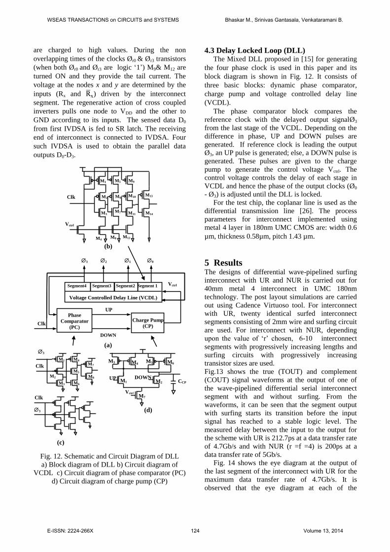
are charged to high values. During the non
overlapping times of the clocks Ør0 & Ør3 transistors
(when both Ør0 and Ør3 are logic „1‟) M9& M12 are
turned ON and they provide the tail current. The
voltage at the nodes x and y are determined by the
inputs (Rx and ) driven by the interconnect
segment. The regenerative action of cross coupled
inverters pulls one node to VDD and the other to
GND according to its inputs. The sensed data D0
from first IVDSA is fed to SR latch. The receiving
end of interconnect is connected to IVDSA. Four
such IVDSA is used to obtain the parallel data
outputs D0-D3.
(b)
(a)
(d)
(c)
Fig. 12. Schematic and Circuit Diagram of DLL
a) Block diagram of DLL b) Circuit diagram of
VCDL c) Circuit diagram of phase comparator (PC)
d) Circuit diagram of charge pump (CP)
4.3 Delay Locked Loop (DLL) The Mixed DLL proposed in [15] for generating
the four phase clock is used in this paper and its
block diagram is shown in Fig. 12. It consists of
three basic blocks: dynamic phase comparator,
charge pump and voltage controlled delay line
(VCDL).
The phase comparator block compares the
reference clock with the delayed output signalØ3
from the last stage of the VCDL. Depending on the
difference in phase, UP and DOWN pulses are
generated. If reference clock is leading the output
Ø3, an UP pulse is generated; else, a DOWN pulse is
generated. These pulses are given to the charge
pump to generate the control voltage Vctrl. The
control voltage controls the delay of each stage in
VCDL and hence the phase of the output clocks (Ø0
- Ø3) is adjusted until the DLL is locked.
For the test chip, the coplanar line is used as the
differential transmission line [26]. The process
parameters for interconnect implemented using
metal 4 layer in 180nm UMC CMOS are: width 0.6
µm, thickness 0.58µm, pitch 1.43 µm.
5 Results The designs of differential wave-pipelined surfing
interconnect with UR and NUR is carried out for
40mm metal 4 interconnect in UMC 180nm
technology. The post layout simulations are carried
out using Cadence Virtuoso tool. For interconnect
with UR, twenty identical surfed interconnect
segments consisting of 2mm wire and surfing circuit
are used. For interconnect with NUR, depending
upon the value of „r‟ chosen, 6-10 interconnect
segments with progressively increasing lengths and
surfing circuits with progressively increasing
transistor sizes are used. Fig.13 shows the true (TOUT) and complement
(COUT) signal waveforms at the output of one of
the wave-pipelined differential serial interconnect
segment with and without surfing. From the
waveforms, it can be seen that the segment output
with surfing starts its transition before the input
signal has reached to a stable logic level. The
measured delay between the input to the output for
the scheme with UR is 212.7ps at a data transfer rate
of 4.7Gb/s and with NUR (r =f =4) is 200ps at a
data transfer rate of 5Gb/s. Fig. 14 shows the eye diagram at the output of
the last segment of the interconnect with UR for the
maximum data transfer rate of 4.7Gb/s. It is
observed that the eye diagram at each of the
M1
0
Vctrl
Clk M2
M3
M4
M5
M6
M7
M8
M9
M10
M11
M12
M13
M14
3
2
1
0
Segment4 Segment3 Segment2 Segment 1
Voltage Controlled Delay Line (VCDL)
Clk
Vctrl
DOWN
UP
Phase
Comparator
(PC)
Charge Pump
(CP)
M3
M1
M2
M4
M5
M6
M7
M8
3
Clk
UP
3
Clk
DOWN
v1 UP DOWN
M3 M4
M1
M7 Vctrl
Vctrl
M6 M5
M2 CCP
WSEAS TRANSACTIONS on CIRCUITS and SYSTEMS Bhaskar M., Srinivas Gantasala, Venkataramani B.
E-ISSN: 2224-266X 124 Volume 13, 2014

segment is same and also the swing and the eye
width at all the segments are identical.
The eye diagram at the output of the receiver for
the interconnect with NUR (for „r‟= 4) for 5Gb/s
data transfer rate is shown in Fig. 15. From Fig. 15,
it can be seen that the swing and width of the eye at
the output of the receiver is better because of the
receiver sense amplifier.
Fig. 13 Wave forms showing the effect of surfing in
TOUT and COUT signals
Fig. 14 Eye diagram at the end of the receiver of
serial interconnect with UR at 4.7Gb/s
For the proposed surfing interconnect with UR
and NUR the jitter performance is also carried out
with a jitter of 80ps in the serial input. It is 36% for
UR and 33.6% for NUR of the input signal time
period respectively. The eye diagram of the UR link
at the receiver end with jitter is shown in Fig. 16.
From Fig. 16, it can be observed that the proposed
surfing circuit with UR has no degradation in the
performance and the data signals are received
properly even with 36% of jitter in the input.
In order to compare the performance of surfing
interconnect with UR and NUR, the delay of the
longest segments, the maximum operating
frequency for various values of „r‟ are found and is
given in Table 3. It may be noted that for „r‟ 2.84,
Ltotal is closest to 40 mm. For other values of „r‟, the
last buffer drives only a smaller segment (so that
total length becomes 40 mm) than what is reported
in Table 1.
Fig. 15 Eye diagram at the end of the receiver of
serial interconnect with NUR at 5.0Gb/s
Fig. 16 Eye diagram at the end of the receiver of
serial interconnect with UR at 4.5Gb/s with input
jitter of 80ps
From Table 3, it may be noted that the highest
operating frequency increases with „r‟. For the
purpose of comparison, the power dissipated by the
entire link consisting of the transmitter, surfing
interconnect with NUR and receiver are computed
for different values of „r‟ at a normalized data rate
of 1.55Gb/s and is given in Table 3. The power
consumed by the link with the surfing interconnect
with UR at 1.55Gb/s is 20.89mW. It may be noted
that the power consumed by the NUR is lower
because the transmitter drives a 0.05 mm
interconnect segment, where as in the case of UR it
TIN
CIN
TOUT
TOUT
COUT
COUT
TOUT without surfing
TOUT with surfing
COUT without surfing
COUT with surfing
Time (ns)
V
TIN
CIN
TOUT
COUT
Time (ps)
V
TIN
CIN
TOUT
COUT
Time (ps)
V
TIN
CIN
TOUT
COUT
Time (ps)
V
WSEAS TRANSACTIONS on CIRCUITS and SYSTEMS Bhaskar M., Srinivas Gantasala, Venkataramani B.
E-ISSN: 2224-266X 125 Volume 13, 2014

drives 2mm interconnect segment.
The performance comparison of the single ended
wave pipelined interconnect, the differential wave
pipe-lined serial interconnect with surfing proposed
for UR and NUR in [15] and the proposed self
controllable surfing for differential wave-pipelined
serial interconnect for UR and NUR are given in
Table 4.
Table 3
Delay and power of the interconnect with NUR for
different interconnect ratio
Ratio of interconnect
segments
(r)
Delay of the
longest segment
in NUR(ps)
Max. operating
frequency in
Gb/s
Power consumed at
1.55Gb/s in
(mW)
In
[15]
This
paper
In
[15]
This
paper
In
[15]
This
paper
2.00 643.0 384.6 1.55 2.60 3.8 7.84
3.00 366.0 340.0 2.73 2.94 7.1 10.84
3.50 304.2 280.0 3.28 3.57 10.6 11.92
4.00 250.0 200.0 4.00 5.00 14.0 17.84
4.50 210.3 180.0 4.75 5.55 17.5 29.00
5.00 181.0 166.0 5.52 6.02 22.7 42.00
From Table 4, it is observed that the minimum data
period required for the data transmission through the
entire 20 segment UR surfing interconnect is
212.7ps, which corresponds to serial data transfer
rate of 4.7Gb/s. The data transfer rate of surfing
interconnect with UR and NUR (r=4) are 1.18 and
1.25 times higher than that reported in [15]
respectively. Both surfing interconnects with UR
and NUR allow input jitter of about 36% and 33.6%
of the data period respectively, which is higher than
that reported in [15].
The power consumed and area for the differential
serial interconnect with UR and NUR are given
Table 4. It is observed that the serial interconnect
with NUR consumes lower power by a factor of
3.08 and 2.66 to that of serial interconnect with UR
at a data rate of 4.7Gb/s and 1.55Gb/s respectively.
It is also observed that the area of the serial
interconnect with NUR is lower by a factor of 2.3 as
compared to serial interconnect with UR.
The power consumed by the proposed scheme is
higher both for UR and NUR compared to that
reported in [15] but the area required for surfing
circuit is less both in UR and NUR by a factor of
2.16 and 2.40 respectively compared to that reported
in [15].
Table 4
Performance comparison of the proposed differential wave-pipelined surfing with UR and NUR
with single ended scheme and differential scheme proposed in [15]
Parameters
Single
ended
surfing scheme
[13]
Differential surfing
scheme with UR [15]
Differential surfing
scheme with NUR (r = f = 4)[15]
Differential surfing
scheme with UR
Differential surfing
scheme with NUR (r = f = 4)
Controllable inverter pair for surfing proposed in
[15]
Dynamic self controllable inverter pair for surfing
proposed in this paper
Length of each segment
2mm 2mm 0.05 mm (min.) 22.95 mm(max.)
2mm 0.05 mm (min.) 22.95 mm(max.)
Number of segments
20 20 6 20 6
Width of the
Interconnect
Double the
min. width
0.56µm(Min. width in
0.28µm)
Double the min. width
(0.56 µm)
0.56µm(Min. width in
0.28µm)
Double the min. Width
(0.56 µm)
Delay of each segment
750ps
250ps 16ps(least delay) 250ps(max delay)
250ps 14ps(least delay) 200ps(max delay)
Maximum data transfer rate
1.33Gb/s 4Gb/s 4Gb/s (r = f = 4)
1.55Gb/s (r = f = 2) 5.52Gb/s (r = f =5)
4.7Gb/s 5Gb/s (r = f = 4)
2.66Gb/s (r = f = 2) 6.00Gb/s (r = f =5)
Control signal and
setup time constraint
Yes No No No No
Maximum
allowable Jitter
7.3 % of
data period
24.2% of the data
period 24% of the data period 36% of the data period 33.6% of the data period
Noise Problem Yes No(since the scheme is
differential) No
No(since the scheme is
differential) No
Power -
19.0mW (at 4Gb/s) 5.90mW(at 1.55Gb/s)
11.6mW (at 4Gb/s) 3.80mW (at 1.55Gb/s)
36.00mW (at 4.7Gb/s)
29.42mW (at 4Gb/s) 20.89mW(at 1.55Gb/s)
12.76mW (at 5Gb/s)
9.28mW (at 4Gb/s) 7.84mW (at 1.55Gb/s)
Area of repeaters -
0.05184mm2
0.02765mm2
0.024mm2
0.0115mm2
Control circuitry yes yes No(self controllable) No(self controllable)
WSEAS TRANSACTIONS on CIRCUITS and SYSTEMS Bhaskar M., Srinivas Gantasala, Venkataramani B.
E-ISSN: 2224-266X 126 Volume 13, 2014

Fig. 17. Layout of Transmitter, Dynamic self
controllable surfing circuit and receiver
The layout of the transmitter for true and
complement inputs along with its DLL, the dynamic
self controllable surfing circuit and the receiver
circuit for four data outputs along with its DLL are
shown in Fig. 17.
The synchronization of the transmitter and the
receiver is done using source synchronous clocks.
The clock for the receiver DLL is sent from the
transmitter DLL with the same amount of data
delay. In the complete link design, the transmitter
and receiver DLLs are kept close. The delay
between the input of the transmitter to the input of
the receiver is measured and the same amount of
delay is introduced in the clock path by inserting
buffers and by adjusting their delays.
6 Conclusion
In this paper, dynamic self controllable inverter pair
is proposed for surfing the differential wave pipe-
lined serial interconnect. The design of the
transceiver with self controllable surfing scheme for
uniform repeater and non uniform repeater insertion
is carried out using the method of logical effort and
their performances are compared. The proposed
surfing interconnect with UR and NUR have higher
data transfer rates and allow higher input jitter. The
proposed schemes can be used for higher data
transfer rates through differential on-chip global
interconnect.
References:
[1] International Technology Roadmap for
Semiconductors, (2001). Semiconductor
Industry Association, 2001, Interconnects
section, p. 4.
[2] R.Ho, K.W.Mai, and M.A.Horowitz, “The
future of wires,” Proc. IEEE, vol. 89, no 4,
2001, pp. 490-504.
[3] H.B. Bakoglu, and J.D. Meindl, “Optimal
interconnection circuits for VLSI,” IEEE Trans.
Electron Devices ED-32 (5), 1985, pp. 903–
909.
[4] C.J. Alpert, A. Devgan, J.P. Fishburn, and S.T.
Quay, “Interconnect synthesis without wire
tapering, ” IEEE Trans. Computer-Aided
Design Integrated Circuits and Systems 20 (1),
2001, pp. 90–104.
[5] H. Zhang, V. George, and J. M. Rabaey,
“Low-Swing On-Chip Signaling Techniques:
Effectiveness and Robustness, ”IEEE Trans.
Very Large Scale Integration (VLSI) Systems,
vol. 8, no.3, 2000.
[6] Y.I. Ismail, and E.G. Friedman, Effects of
Inductance on the propagation delay and
repeater insertion in VLSI circuits, IEEE Trans.
Very Large Scale Integration Systems 8 (2),
2000, pp. 195–206.
[7] G.Chen and E.G.Friedman, Low-Power
Repeaters Driving RC and RLC Interconnects
with delay and bandwidth constraints, IEEE
Trans. Very Large Scale Integration (VLSI)
Systems, vol. 14, no.2, 2006.
[8] R. T. Chang, N. Talwalkar, C. P. Yue, and S.
S.Wong, Near speed of light signaling over on-
chip electrical interconnects, IEEE J. Solid-
State Circuits, vol. 34, no. 5, 2003, pp. 834–
838.
[9] P.Wang, G. Pei and E. chih-chuanKan, “Pulsed
wave interconnect,” IEEE Trans. Very Large
Scale Integration (VLSI) Systems, vol. 12, no.
5, 2004.
[10] A. P. Jose, G. Patounakis, and K. L. Shepard,
“Pulsed current-mode signaling for nearly
speed-of- light intra-chip communication, ”
IEEE Journal of Solid-State Circuits, vol. 41,
2006, pp. 772-780.
[11] M. J. E. Lee,W.J.Dally and P. Chiang , Low-
power area efficient high speed I/O circuit
techniques, IEEE Journal of Solid-State
Circuits, vol. 35, 2000, pp. 1591-1599.
[12] J. Nyathi, R.R. Rydberg III and J.G. Delgado-
Frias, “Wave-Pipelining the Global
Interconnect to Reduce the Associated Delays,”
IEEE conference, 2006.
[13] Greenstreet and Ren, “Surfing Interconnect,” In
Proceedings of the 12th IEEE International
Symposium on Asynchronous Circuits and
Systems (ASYNC‟06).
[14] M.Bhaskar, D.Parthiban and B.Venkataramani,
“Design and Implementation of surfing scheme
to wave pipelined differential serial
interconnect,” IEEE - RAICS conference 2011.
WSEAS TRANSACTIONS on CIRCUITS and SYSTEMS Bhaskar M., Srinivas Gantasala, Venkataramani B.
E-ISSN: 2224-266X 127 Volume 13, 2014

[15] M. Bhaskar , A. Jaswanth, B. Venkataramani,
“Design of a novel differential on-chip wave-
pipelined serial interconnect with surfing,”
Microprocessor and Microsystems, Elsevier
(37), 2013, pp. 649-660.
[16] I. Sutherland, B. Sproull, and D.
Harris,“Logical Effort: Designing Fast CMOS
Circuits, ”Morgan Kaufmann Publishers, Inc.,
1998.
[17] Cadence user manual - Mixed mode RF
CMOS, ver. 2.0.
[18] J.Rabey, A.Chandrakasan and B.Nikolic, “
Digital Integrated Circuits: A Design
perspective,” 2/e, Prentice Hall, 2003.
[19] P.Murugeswari, G.Anusha, P.Venkateshwarlu,
M.Bhaskar, and B.Venkataramani, “A Wide
Band Voltage Mode Sense Amplifier Receiver
for High Speed Interconnects,” Proceedings of
TENCON 2008, IEEE Region 10 conference.
[20] X. Sun and J. Feng, “A 10Gb/s Low-power 4:1
multiplexer in 0.18 µm CMOS,” Proc. of
ISSSE, 2010.
[21] P.Wijetunga and A.F.J. Levi, “3.3 GHz Sense-
amplifier in 0.18 µm CMOS technology,”
IEEE, ISCAS, 2002, pp. 764-765.
[22] Karutharaja.V, M.Bhaskar and
B.Venkataramani, “Synchronization of On-chip
Serial Interconnect Transceivers using Delay
Locked Loop (DLL),” Proceeding of 2011
IEEE International conference ICSCCN, 2011.
[23] Y Moon, J Choi, K Lee, D-K Jeong, M-K Kim,
“An All Analog Multiphase Delay-Locked
Loop Using a Replica Delay Line for Wide
range Operation and Low-Jitter Performance,”
IEEE Journal of Solid-State Circuits, Vol. 35,
No.3, 2000.
[24] S. Kim, K.Lee, Y.Moon, D.K.Jeong, Y.Choi
and H.K.Lim, “A 960-Mb/s/pin Interface for
skew tolerant bus using low jitter PLL,”IEEE J.
Solid-State Circuits, vol. 32, 1977, pp. 691-
700.
[25] Mark G. Johnson, and Edwin L. Hudson, “A
Variable Delay Line PLL for CPU-
Coprocessor Synchronization,”IEEE Journal of
Solid-State Circuits. Vol. 23, No. 5, October,
1988.
[26] H. Ito, J.Inoue, S. Gomi, H.Sugita, K. Okada
and K. Masu, “On-chip Transmission line for
Long Global Interconnects,” IEEE, IEDM,
2004.
WSEAS TRANSACTIONS on CIRCUITS and SYSTEMS Bhaskar M., Srinivas Gantasala, Venkataramani B.
E-ISSN: 2224-266X 128 Volume 13, 2014


![Controllable Sliding Bearings and Controllable Lubrication ... · Review Controllable Sliding Bearings and Controllable ... or evolutionary [5], but it does not change the fact that](https://static.fdocuments.in/doc/165x107/5fc50df11ca4e1756528a85b/controllable-sliding-bearings-and-controllable-lubrication-review-controllable.jpg)