
Dynamic Logic Families - UCLAicslwebs.ee.ucla.edu/yang/classwiki/images/f/fe/04_ee215b_dyn... · EE...
50
Transcript of Dynamic Logic Families - UCLAicslwebs.ee.ucla.edu/yang/classwiki/images/f/fe/04_ee215b_dyn... · EE...
2EE 215B
Overview
• Reading– Rabaey 6.3 (Dynamic), 7.5.2 (NORA)
• Overview– This set of notes cover in greater detail Dynamic Logic
Families and in particular Domino Logic. There is an extensive discussion on the noise issues in dynamic circuits and how they are resolved. A few variants of domino logic are introduced.
3EE 215B
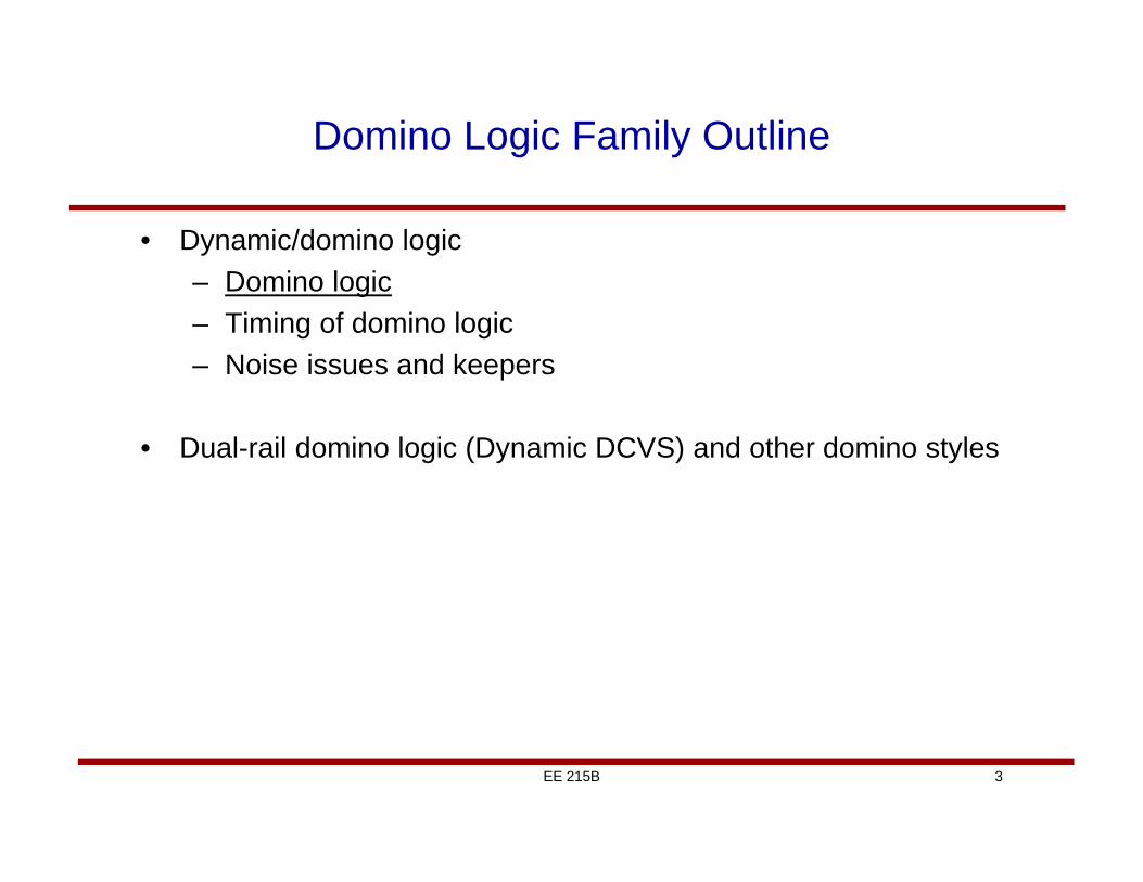
Domino Logic Family Outline
• Dynamic/domino logic– Domino logic– Timing of domino logic– Noise issues and keepers
• Dual-rail domino logic (Dynamic DCVS) and other domino styles
4EE 215B
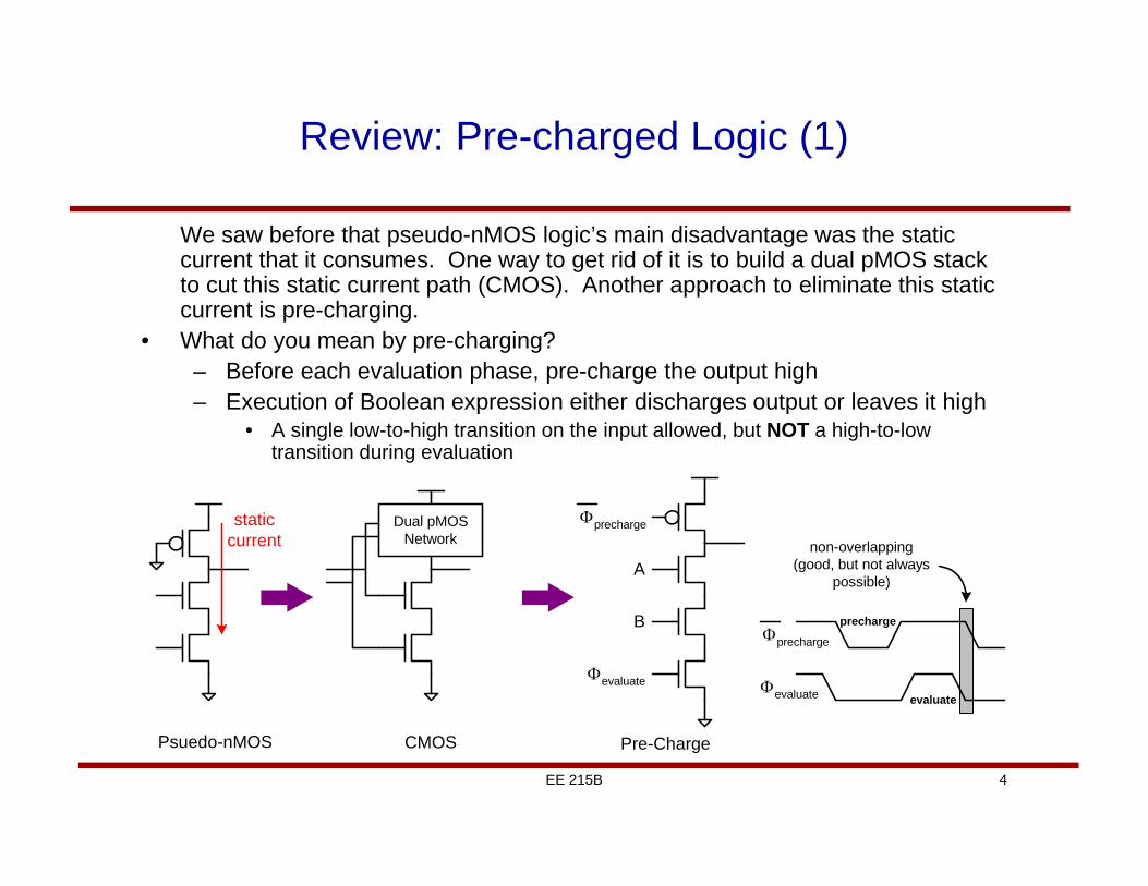
Review: Pre-charged Logic (1)
We saw before that pseudo-nMOS logic’s main disadvantage was the static current that it consumes. One way to get rid of it is to build a dual pMOS stack to cut this static current path (CMOS). Another approach to eliminate this static current is pre-charging.
• What do you mean by pre-charging?– Before each evaluation phase, pre-charge the output high– Execution of Boolean expression either discharges output or leaves it high
• A single low-to-high transition on the input allowed, but NOT a high-to-low transition during evaluation
Dual pMOSNetwork
staticcurrent
A
B
precharge
evaluate evaluate
precharge
non-overlapping(good, but not always
possible)
evaluate
precharge
Psuedo-nMOS CMOS Pre-Charge
5EE 215B
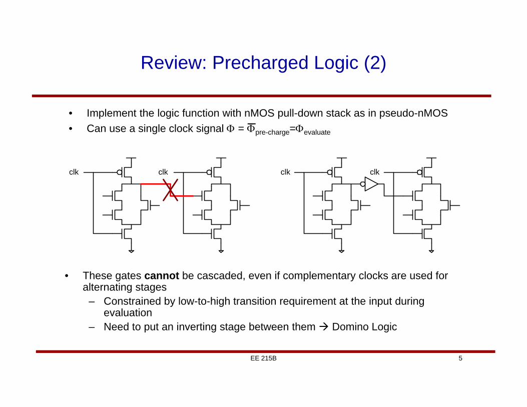
• Implement the logic function with nMOS pull-down stack as in pseudo-nMOS• Can use a single clock signal = pre-charge=evaluate
Review: Precharged Logic (2)
clk clk clk clk
• These gates cannot be cascaded, even if complementary clocks are used for alternating stages
– Constrained by low-to-high transition requirement at the input during evaluation
– Need to put an inverting stage between them Domino Logic
6EE 215B
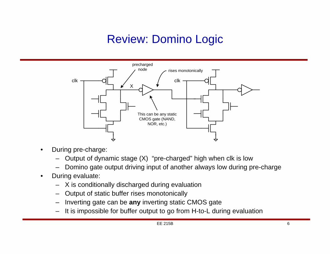
Review: Domino Logic
clk clk
This can be any staticCMOS gate (NAND,
NOR, etc.)
rises monotonicallyprecharged
node
X
• During pre-charge:– Output of dynamic stage (X) “pre-charged” high when clk is low– Domino gate output driving input of another always low during pre-charge
• During evaluate:– X is conditionally discharged during evaluation– Output of static buffer rises monotonically– Inverting gate can be any inverting static CMOS gate – It is impossible for buffer output to go from H-to-L during evaluation
7EE 215B
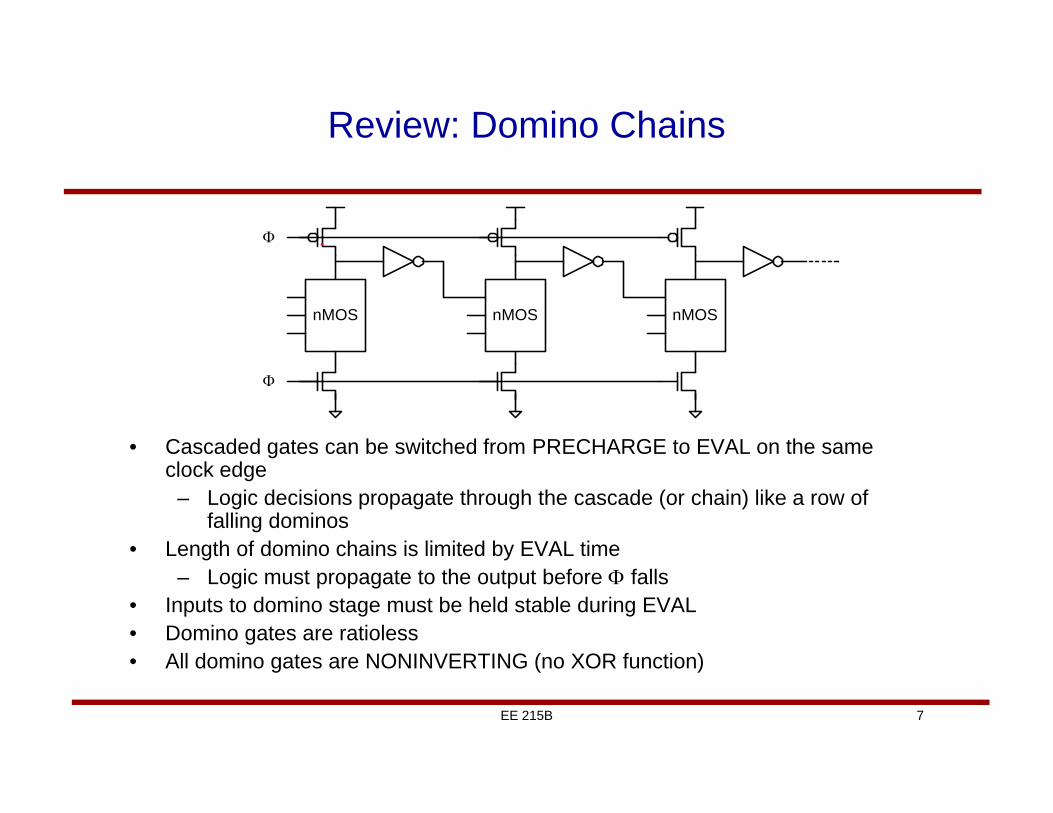
Review: Domino Chains
nMOS nMOS nMOS
• Cascaded gates can be switched from PRECHARGE to EVAL on the same clock edge
– Logic decisions propagate through the cascade (or chain) like a row of falling dominos
• Length of domino chains is limited by EVAL time– Logic must propagate to the output before falls
• Inputs to domino stage must be held stable during EVAL• Domino gates are ratioless• All domino gates are NONINVERTING (no XOR function)
8EE 215B
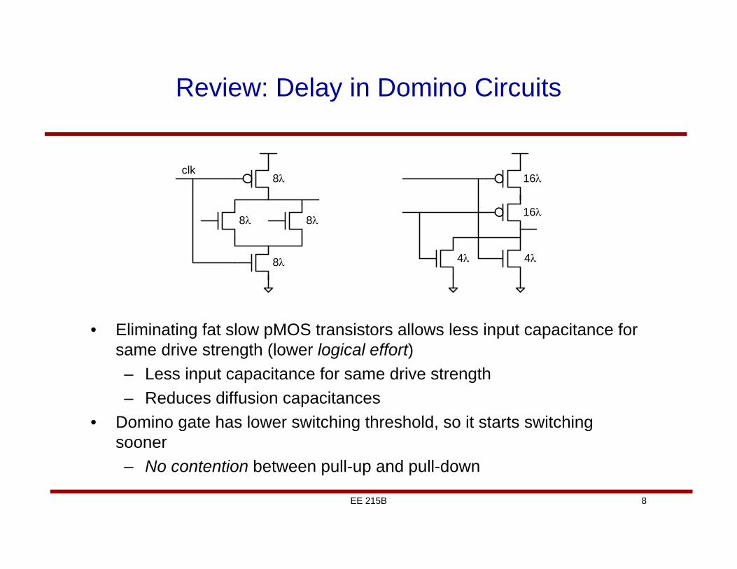
Review: Delay in Domino Circuits
clk8
8 8
8
16
4 4
16
• Eliminating fat slow pMOS transistors allows less input capacitance for same drive strength (lower logical effort)– Less input capacitance for same drive strength– Reduces diffusion capacitances
• Domino gate has lower switching threshold, so it starts switching sooner – No contention between pull-up and pull-down
9EE 215B
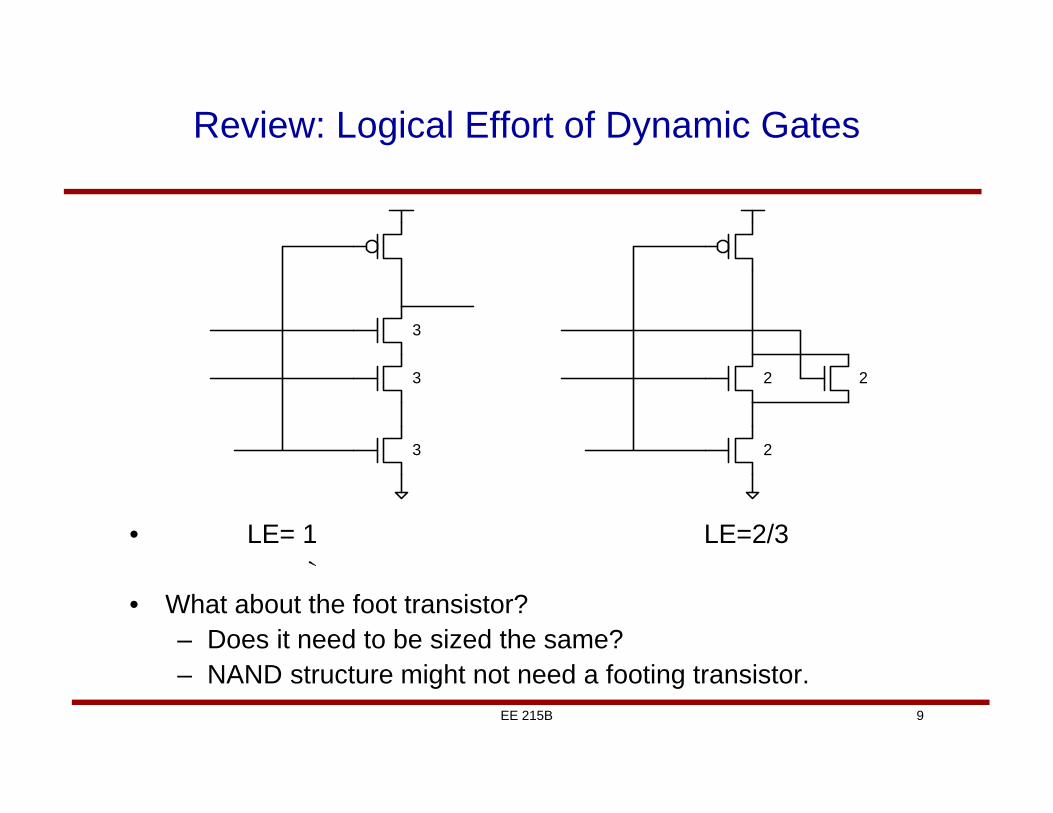
Review: Logical Effort of Dynamic Gates
• LE= 1 LE=2/3
• What about the foot transistor?– Does it need to be sized the same?– NAND structure might not need a footing transistor.
3
3
3
22
2
10EE 215B
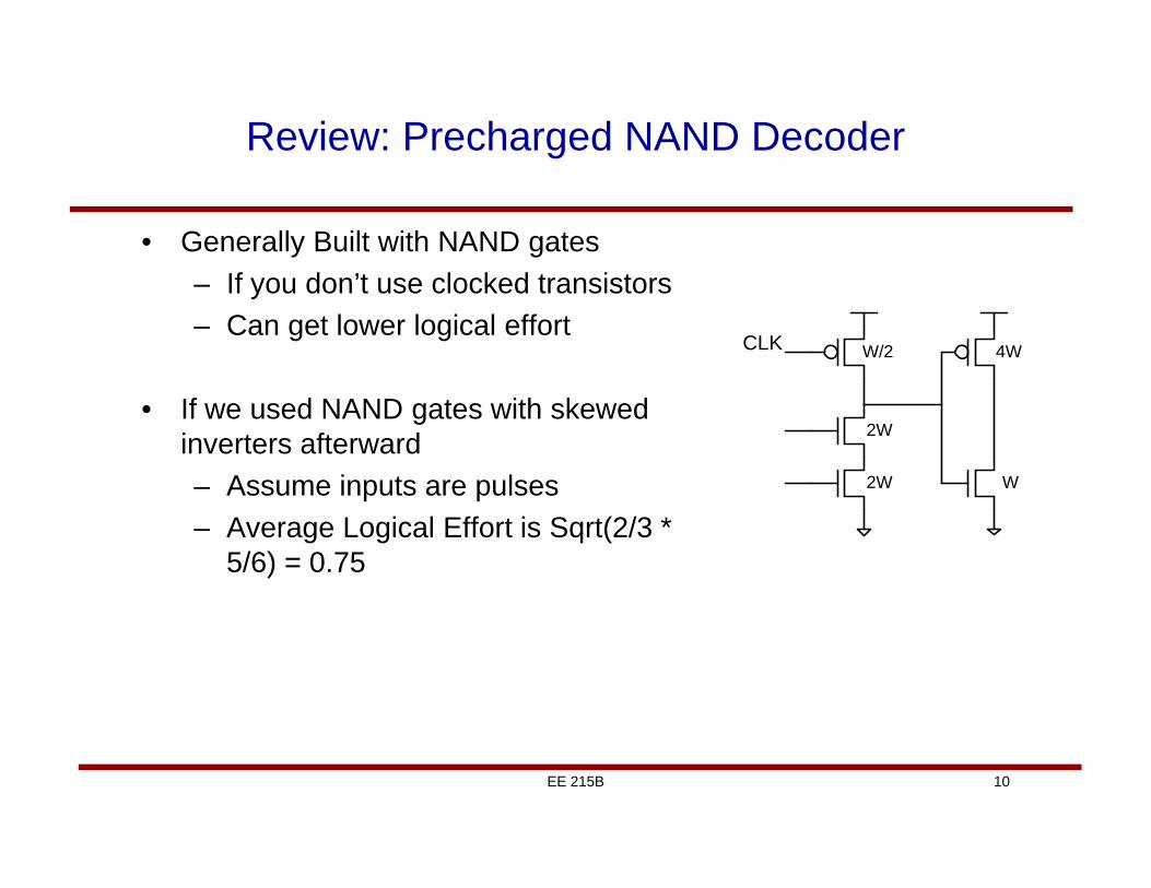
Review: Precharged NAND Decoder
• Generally Built with NAND gates– If you don’t use clocked transistors– Can get lower logical effort
• If we used NAND gates with skewed inverters afterward– Assume inputs are pulses– Average Logical Effort is Sqrt(2/3 *
5/6) = 0.75
W/2
2W
2W W
4WCLK
11EE 215B
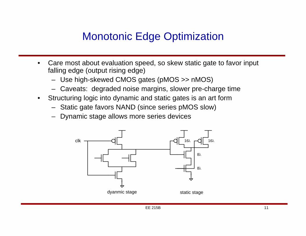
Monotonic Edge Optimization
• Care most about evaluation speed, so skew static gate to favor input falling edge (output rising edge)– Use high-skewed CMOS gates (pMOS >> nMOS)– Caveats: degraded noise margins, slower pre-charge time
• Structuring logic into dynamic and static gates is an art form– Static gate favors NAND (since series pMOS slow)– Dynamic stage allows more series devices
dyanmic stage static stage
clk 16 16
8
8
12EE 215B
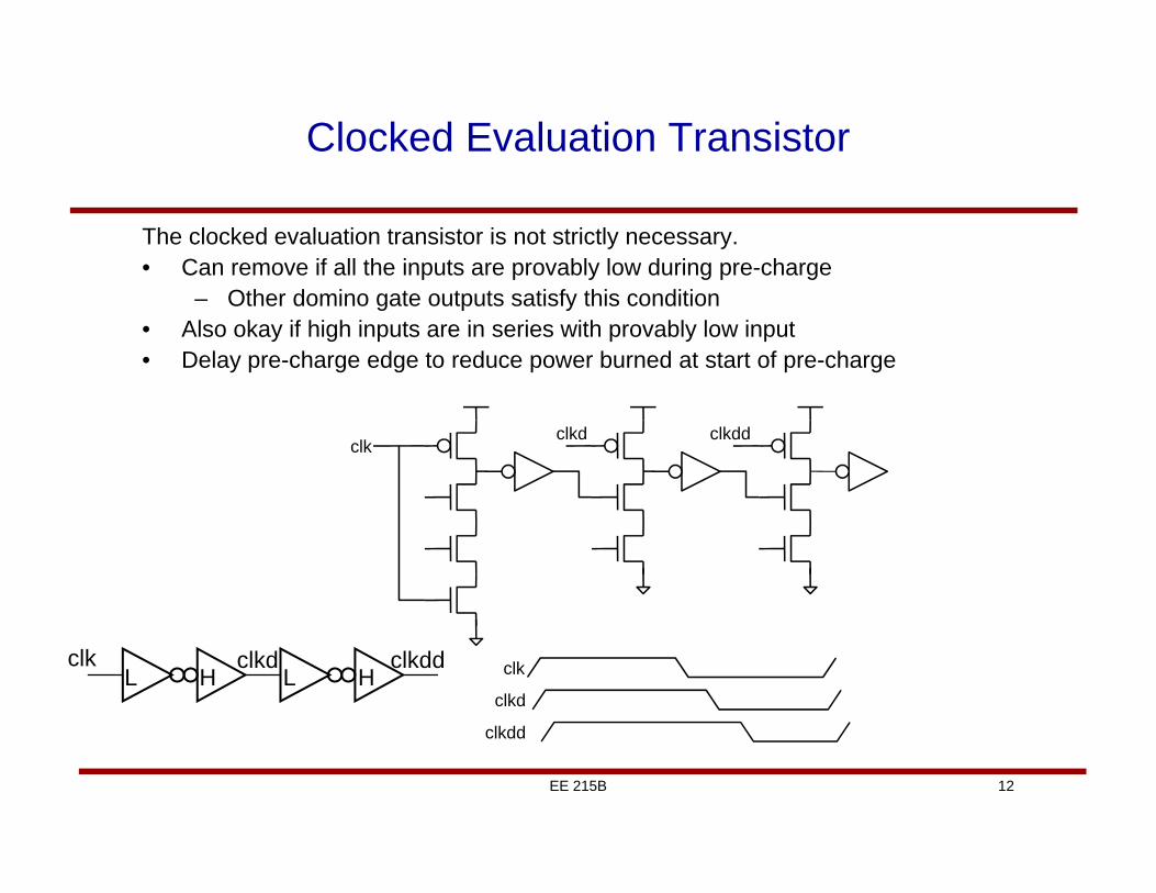
Clocked Evaluation Transistor
The clocked evaluation transistor is not strictly necessary.• Can remove if all the inputs are provably low during pre-charge
– Other domino gate outputs satisfy this condition• Also okay if high inputs are in series with provably low input• Delay pre-charge edge to reduce power burned at start of pre-charge
clk clkd clkddL H L H
clkclkd clkdd
clkd
clkdd
clk
13EE 215B
Pre-charge Properties
• Many domino gates can evaluate in one half-cycle, so it should be easy to pre-charge a single domino gate in the other half-cycle. But…– The domino gate must pre-charge enough to flip the high skew
gate, then the high skew gate must fall below Vt by sufficient noise margin before evaluation starts again
– To speed up domino evaluation, we want a small pre-charge transistor (small diffusion parasitic capacitances)
• Makes pre-charge slow• High skew gate falls very slowly
– Delaying the clock to avoid pre-charge contention in un-clocked pull-down stacks reduces pre-charge time for clkdd domino gate
– Cycles are getting shorter– Advanced domino methodologies are stretching the length of
evaluation phase at the expense of pre-charge time• Bottom line: pre-charge time is becoming an important issue. Size for
roughly equal pre-charge and evaluate times
14EE 215B
Domino Logic Family Outline
• Dynamic/domino logic– Domino logic– Timing of domino logic– Noise issues and keepers
• Dual-rail domino logic (Dynamic DCVS) and other domino styles
15EE 215B
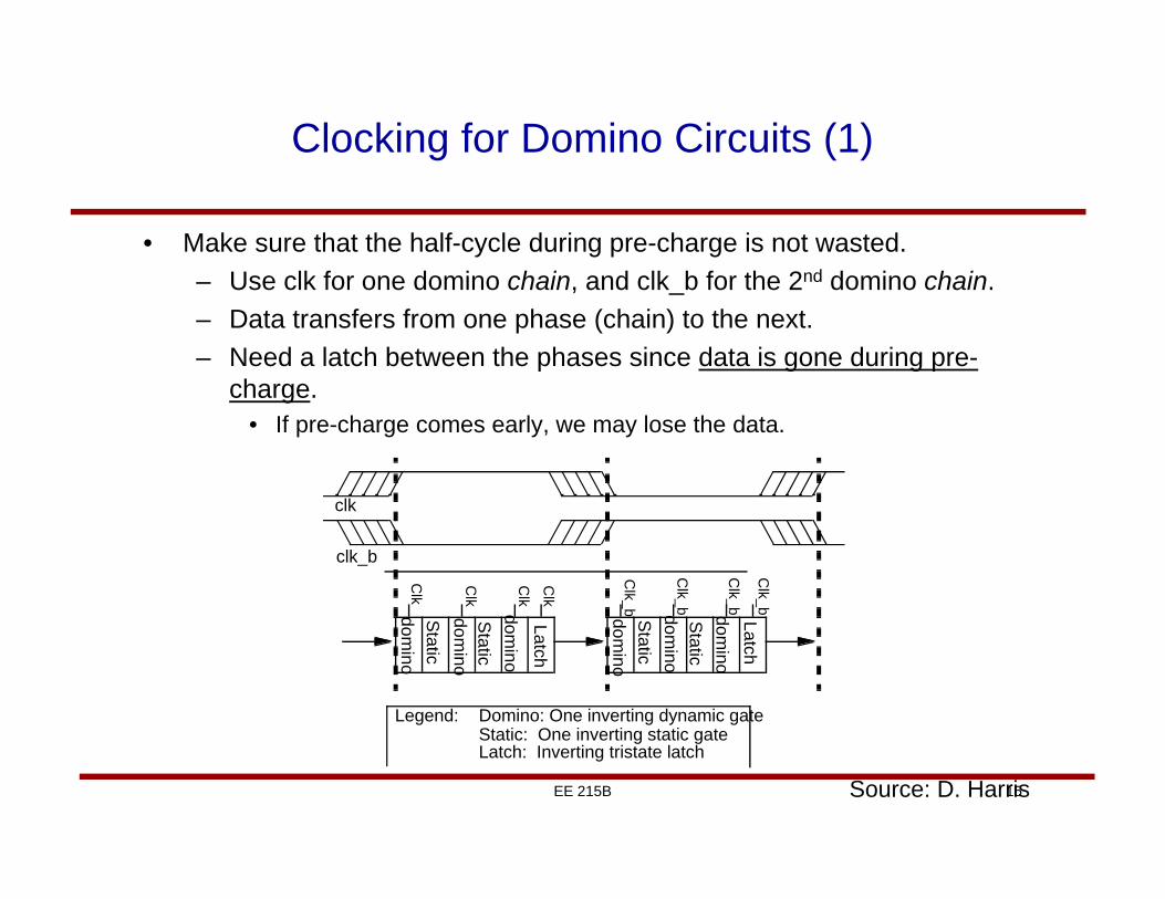
Clocking for Domino Circuits (1)
• Make sure that the half-cycle during pre-charge is not wasted.– Use clk for one domino chain, and clk_b for the 2nd domino chain.– Data transfers from one phase (chain) to the next.– Need a latch between the phases since data is gone during pre-
charge.• If pre-charge comes early, we may lose the data.
clk
clk_b
Clk
Clk_b
Latch
Static
Legend: Static: One inverting static gateDomino: One inverting dynamic gate
Latch: Inverting tristate latch
Source: D. Harris
LatchC
lk_b
Clk_b
Clk_b
Clk
Clk
Clk
Static
Static
Static
domino
domino
domino
domino
domino
domino
16EE 215B
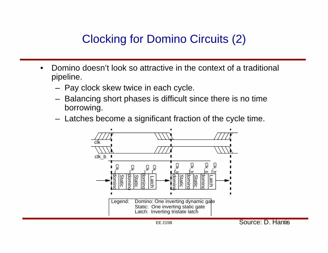
Clocking for Domino Circuits (2)
• Domino doesn’t look so attractive in the context of a traditional pipeline.– Pay clock skew twice in each cycle.– Balancing short phases is difficult since there is no time
borrowing.– Latches become a significant fraction of the cycle time.
clk
clk_b
Clk
Clk_b
Latch
Static
Legend: Static: One inverting static gateDomino: One inverting dynamic gate
Latch: Inverting tristate latch
Source: D. Harris
LatchC
lk_b
Clk_b
Clk_b
Clk
Clk
Clk
Static
Static
Static
domino
domino
domino
domino
domino
domino
17EE 215B
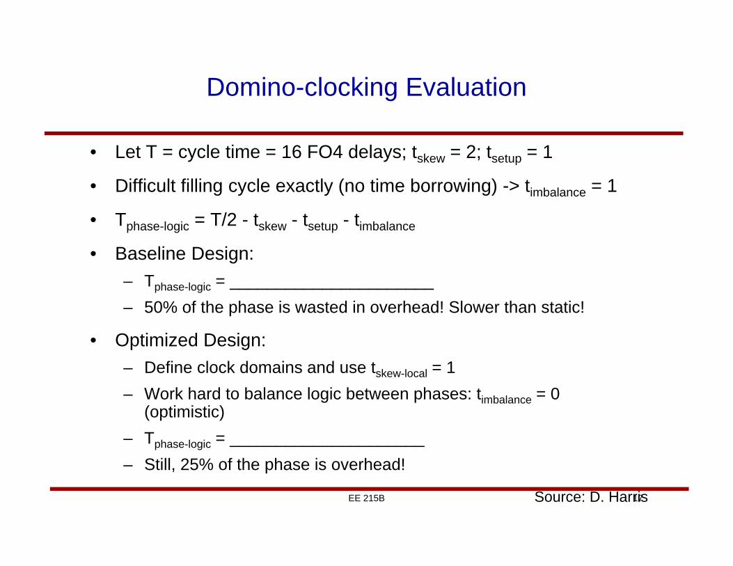
Domino-clocking Evaluation
• Let T = cycle time = 16 FO4 delays; tskew = 2; tsetup = 1
• Difficult filling cycle exactly (no time borrowing) -> timbalance = 1
• Tphase-logic = T/2 - tskew - tsetup - timbalance
• Baseline Design: – Tphase-logic = ______________________– 50% of the phase is wasted in overhead! Slower than static!
• Optimized Design:– Define clock domains and use tskew-local = 1– Work hard to balance logic between phases: timbalance = 0
(optimistic)– Tphase-logic = _____________________– Still, 25% of the phase is overhead!
Source: D. Harris
18EE 215B
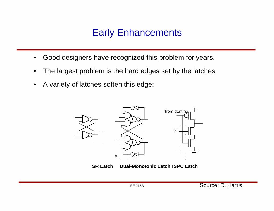
Early Enhancements
• Good designers have recognized this problem for years.
• The largest problem is the hard edges set by the latches.
• A variety of latches soften this edge:
Source: D. Harris
TSPC LatchSR Latch
from domino
Dual-Monotonic Latch
19EE 215B
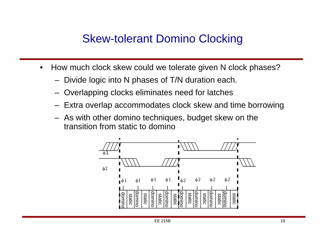
Skew-tolerant Domino Clocking
• How much clock skew could we tolerate given N clock phases?– Divide logic into N phases of T/N duration each.– Overlapping clocks eliminates need for latches– Extra overlap accommodates clock skew and time borrowing– As with other domino techniques, budget skew on the
transition from static to domino
1
2
1 1 1 1 2 2 2 2
static
domino
static
static
static
domino
domino
domino
domino
domino
domino
domino
static
static
static
static
20EE 215B
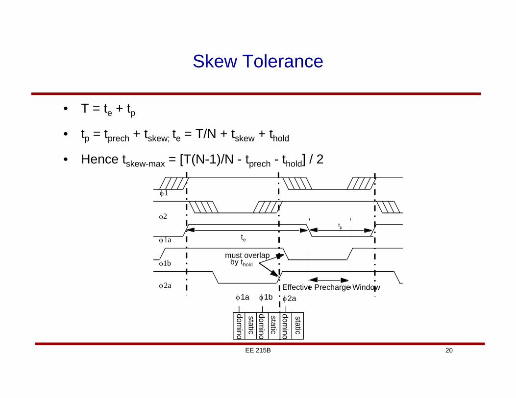
Skew Tolerance
• T = te + tp
• tp = tprech + tskew; te = T/N + tskew + thold
• Hence tskew-max = [T(N-1)/N - tprech - thold] / 2
1
2
1a 1b 2a
1a
1b
2a
te
tp
Effective Precharge Window
must overlapby thold
domino
staticdom
ino
domino
static
static
21EE 215B
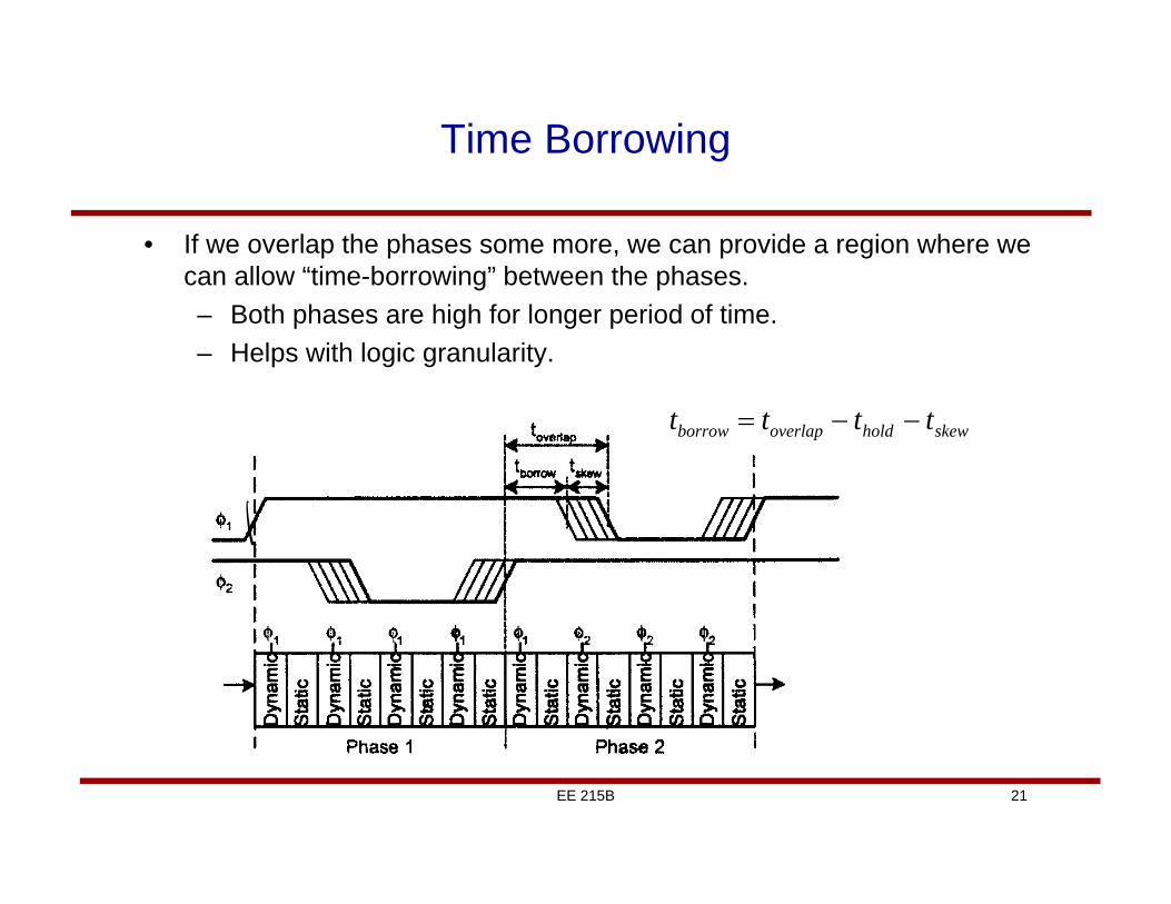
Time Borrowing
• If we overlap the phases some more, we can provide a region where we can allow “time-borrowing” between the phases.– Both phases are high for longer period of time.– Helps with logic granularity.
skewholdoverlapborrow tttt
22EE 215B
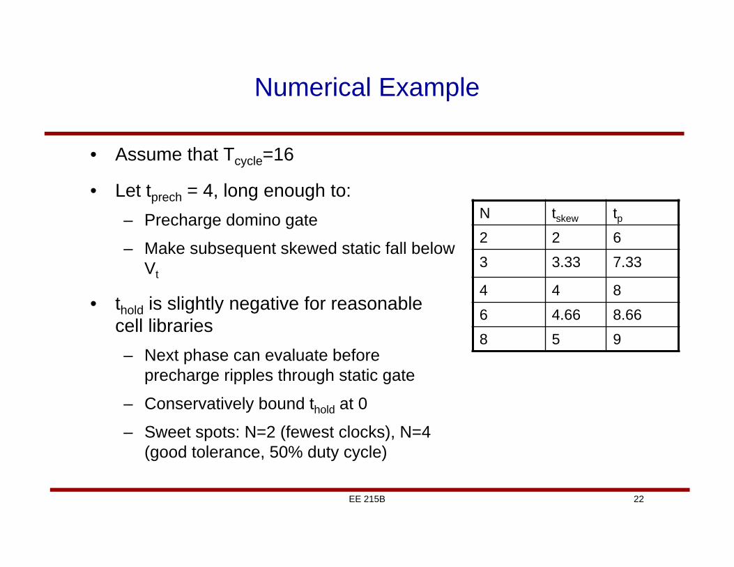
Numerical Example
• Assume that Tcycle=16
• Let tprech = 4, long enough to:– Precharge domino gate
– Make subsequent skewed static fall below Vt
• thold is slightly negative for reasonable cell libraries– Next phase can evaluate before
precharge ripples through static gate
– Conservatively bound thold at 0
– Sweet spots: N=2 (fewest clocks), N=4 (good tolerance, 50% duty cycle)
N tskew tp2 2 63 3.33 7.33
4 4 86 4.66 8.668 5 9
23EE 215B
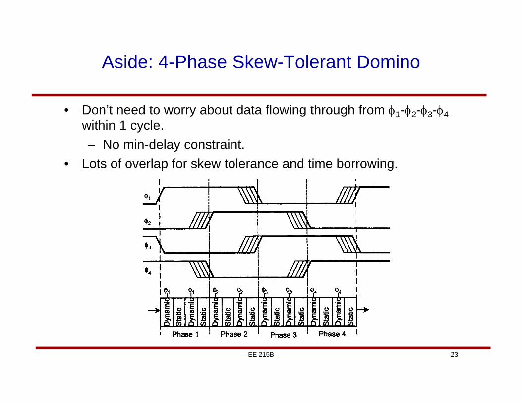
Aside: 4-Phase Skew-Tolerant Domino
• Don’t need to worry about data flowing through from 1-2-3-4within 1 cycle.– No min-delay constraint.
• Lots of overlap for skew tolerance and time borrowing.
24EE 215B
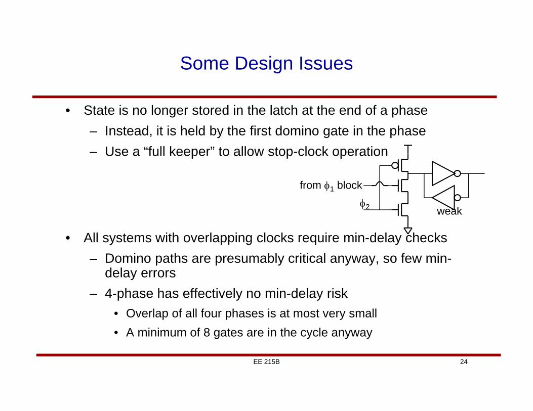
Some Design Issues
• State is no longer stored in the latch at the end of a phase– Instead, it is held by the first domino gate in the phase– Use a “full keeper” to allow stop-clock operation
• All systems with overlapping clocks require min-delay checks– Domino paths are presumably critical anyway, so few min-
delay errors– 4-phase has effectively no min-delay risk
• Overlap of all four phases is at most very small• A minimum of 8 gates are in the cycle anyway
2
from 1 block
weak
25EE 215B
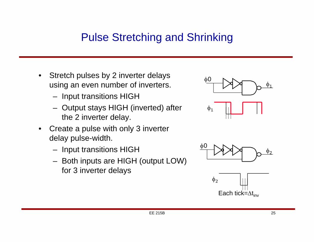
Pulse Stretching and Shrinking
• Stretch pulses by 2 inverter delays using an even number of inverters.– Input transitions HIGH– Output stays HIGH (inverted) after
the 2 inverter delay.• Create a pulse with only 3 inverter
delay pulse-width.– Input transitions HIGH – Both inputs are HIGH (output LOW)
for 3 inverter delays
10
20
2
Each tick=tinv
1
26EE 215B
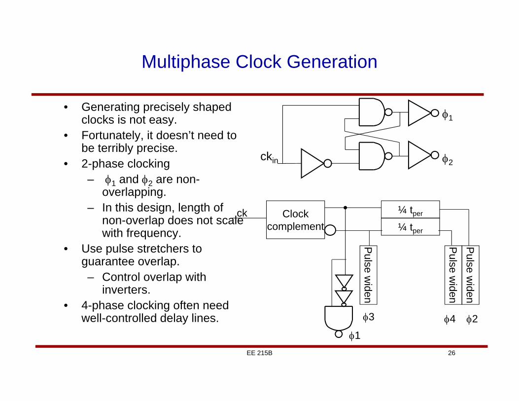
Multiphase Clock Generation
• Generating precisely shaped clocks is not easy.
• Fortunately, it doesn’t need to be terribly precise.
• 2-phase clocking– 1 and 2 are non-
overlapping.– In this design, length of
non-overlap does not scale with frequency.
• Use pulse stretchers to guarantee overlap.– Control overlap with
inverters.• 4-phase clocking often need
well-controlled delay lines.
1
2ckin
¼ tperClockcomplement ¼ tper
Pulse w
iden
Pulse w
idenP
ulse widen
1
3 24
ck
27EE 215B
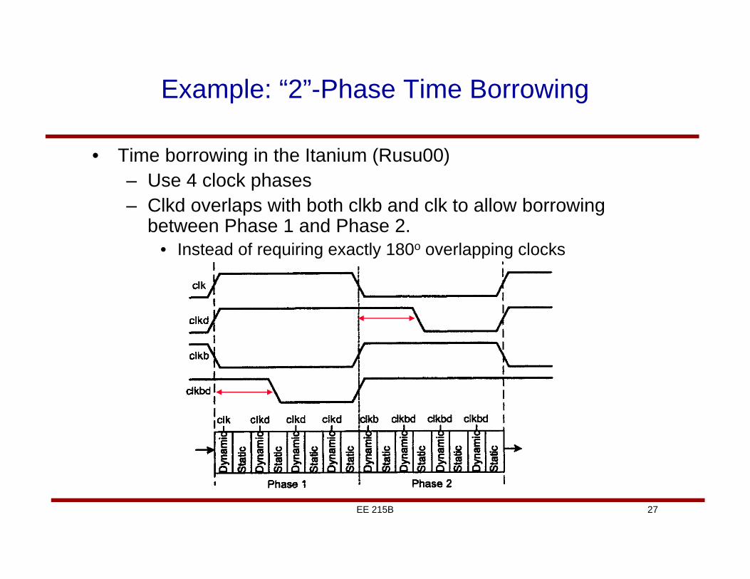
Example: “2”-Phase Time Borrowing
• Time borrowing in the Itanium (Rusu00)– Use 4 clock phases– Clkd overlaps with both clkb and clk to allow borrowing
between Phase 1 and Phase 2.• Instead of requiring exactly 180o overlapping clocks
28EE 215B
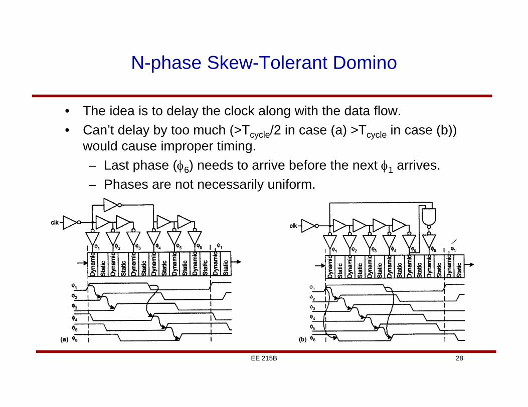
N-phase Skew-Tolerant Domino
• The idea is to delay the clock along with the data flow.• Can’t delay by too much (>Tcycle/2 in case (a) >Tcycle in case (b))
would cause improper timing.– Last phase (6) needs to arrive before the next 1 arrives.– Phases are not necessarily uniform.
29EE 215B
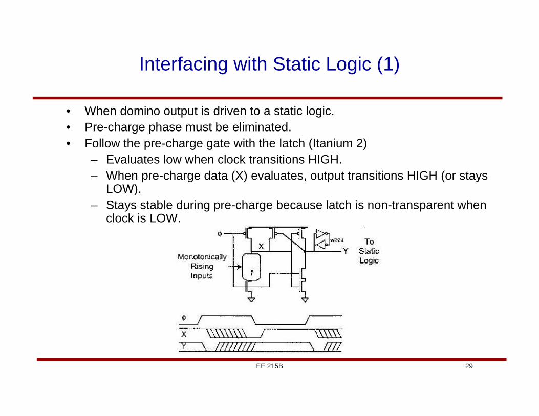
Interfacing with Static Logic (1)
• When domino output is driven to a static logic.• Pre-charge phase must be eliminated.• Follow the pre-charge gate with the latch (Itanium 2)
– Evaluates low when clock transitions HIGH.– When pre-charge data (X) evaluates, output transitions HIGH (or stays
LOW).– Stays stable during pre-charge because latch is non-transparent when
clock is LOW.
30EE 215B
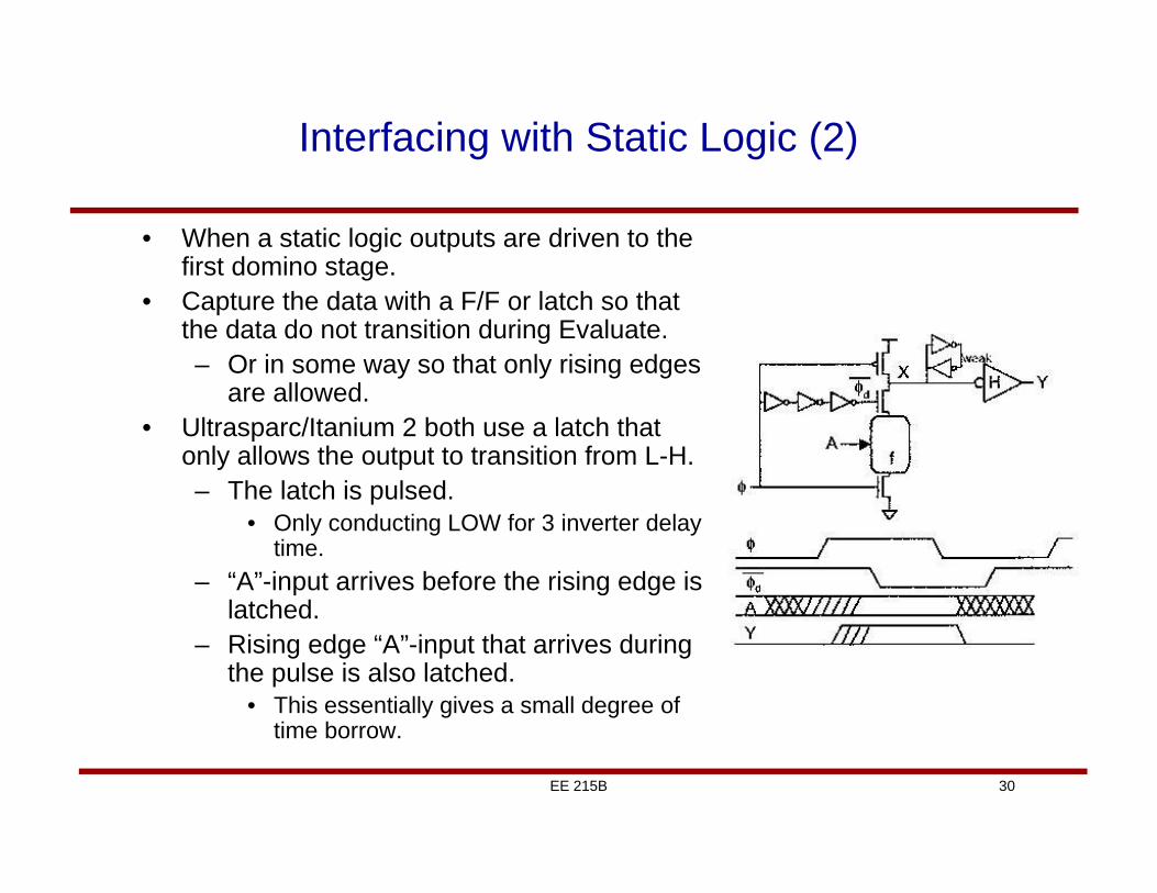
Interfacing with Static Logic (2)
• When a static logic outputs are driven to the first domino stage.
• Capture the data with a F/F or latch so that the data do not transition during Evaluate.– Or in some way so that only rising edges
are allowed.• Ultrasparc/Itanium 2 both use a latch that
only allows the output to transition from L-H.– The latch is pulsed.
• Only conducting LOW for 3 inverter delay time.
– “A”-input arrives before the rising edge is latched.
– Rising edge “A”-input that arrives during the pulse is also latched.
• This essentially gives a small degree of time borrow.
31EE 215B
Domino Logic Family Outline
• Dynamic/domino logic– Domino logic– Timing of domino logic– Noise issues and keepers
• Dual-rail domino logic (Dynamic DCVS) and other domino styles
32EE 215B
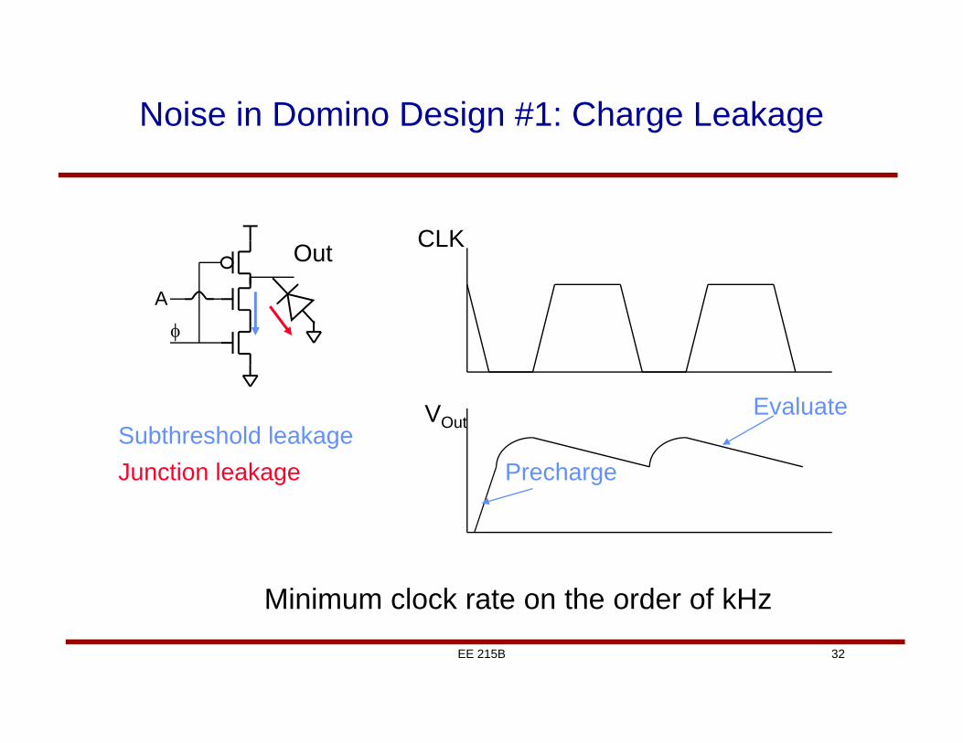
Noise in Domino Design #1: Charge Leakage
Out
Minimum clock rate on the order of kHz
Subthreshold leakage
CLK
VOut
Precharge
Evaluate
A
Junction leakage
33EE 215B
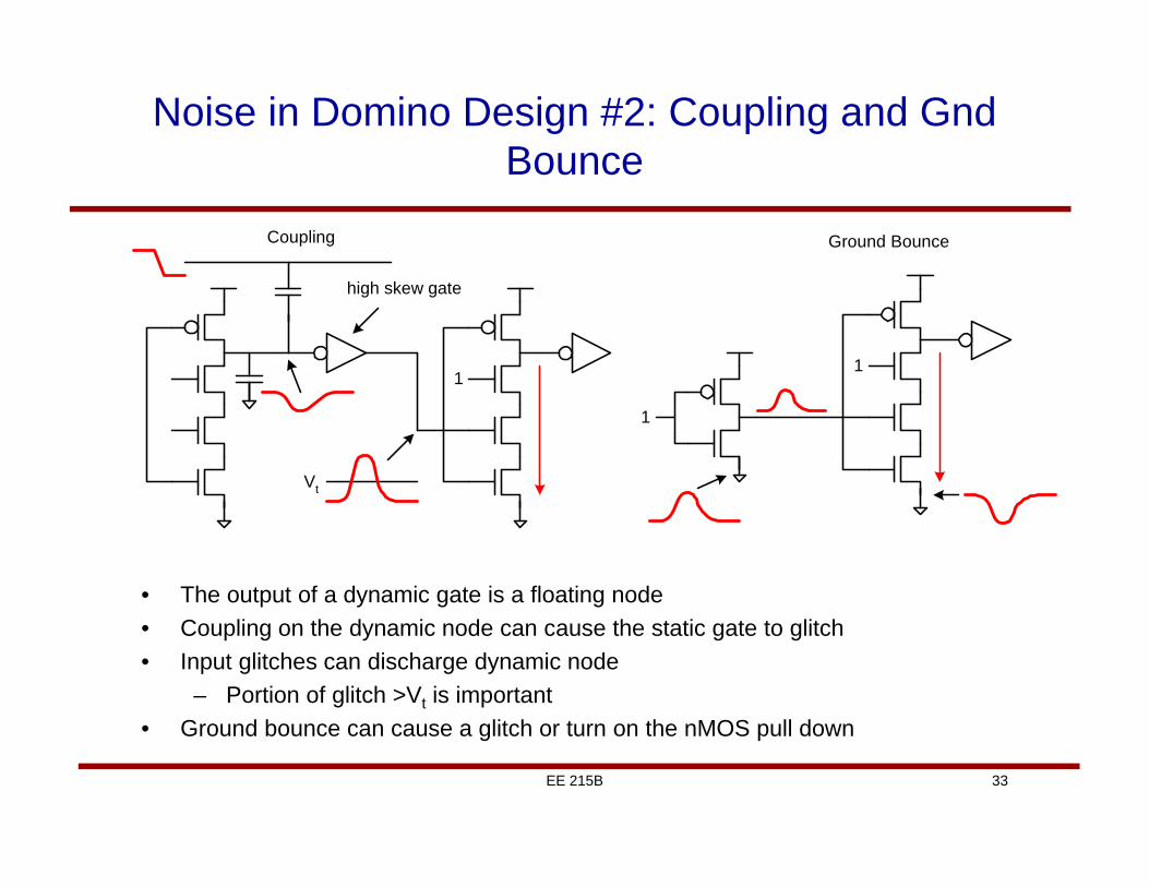
Noise in Domino Design #2: Coupling and Gnd Bounce
Vt
1
high skew gate
1
1
Coupling Ground Bounce
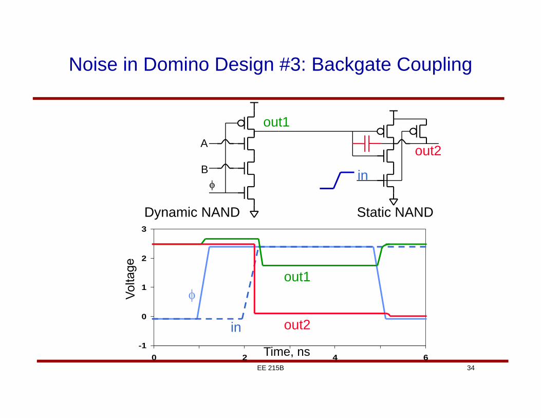
• The output of a dynamic gate is a floating node• Coupling on the dynamic node can cause the static gate to glitch• Input glitches can discharge dynamic node
– Portion of glitch >Vt is important• Ground bounce can cause a glitch or turn on the nMOS pull down
34EE 215B
-1
0
1
2
3
0 2 4 6
Noise in Domino Design #3: Backgate Coupling
Dynamic NAND Static NAND
Time, ns
in
out1
out2
A
B in
out1
out2
35EE 215B
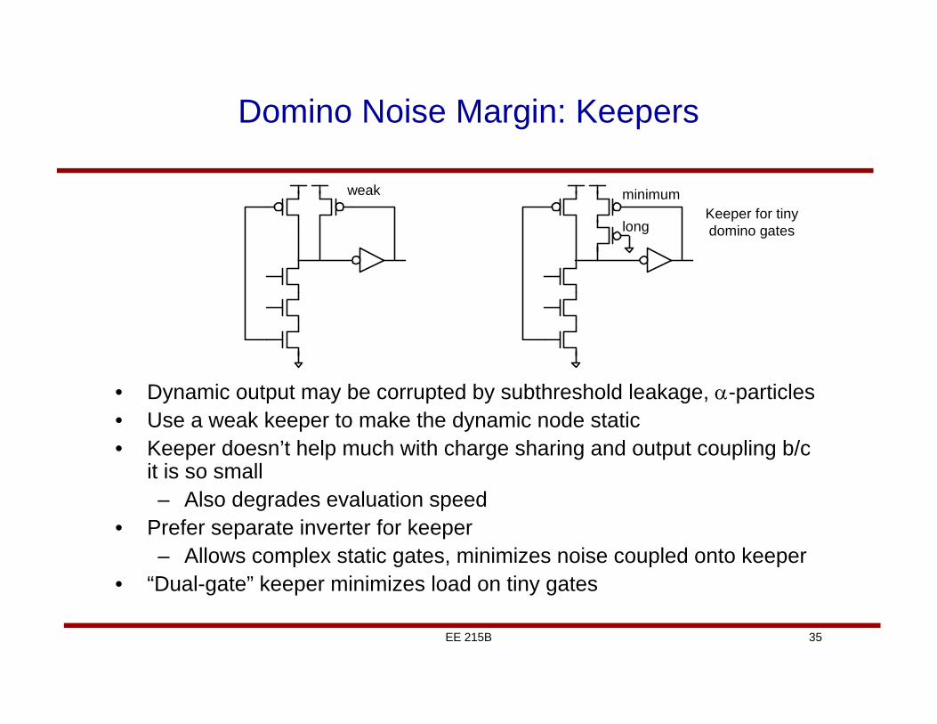
Domino Noise Margin: Keepers
weak minimum
longKeeper for tinydomino gates
• Dynamic output may be corrupted by subthreshold leakage, -particles• Use a weak keeper to make the dynamic node static• Keeper doesn’t help much with charge sharing and output coupling b/c
it is so small– Also degrades evaluation speed
• Prefer separate inverter for keeper– Allows complex static gates, minimizes noise coupled onto keeper
• “Dual-gate” keeper minimizes load on tiny gates
36EE 215B
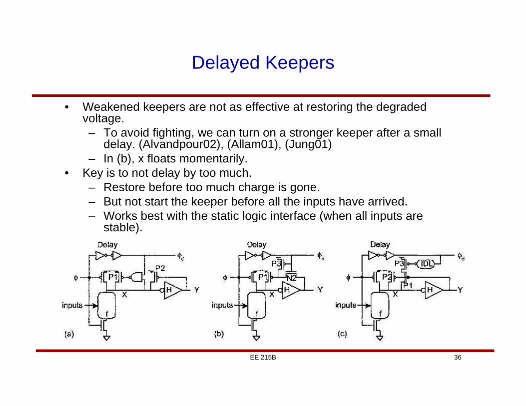
Delayed Keepers
• Weakened keepers are not as effective at restoring the degraded voltage.– To avoid fighting, we can turn on a stronger keeper after a small
delay. (Alvandpour02), (Allam01), (Jung01)– In (b), x floats momentarily.
• Key is to not delay by too much.– Restore before too much charge is gone.– But not start the keeper before all the inputs have arrived.– Works best with the static logic interface (when all inputs are
stable).
37EE 215B
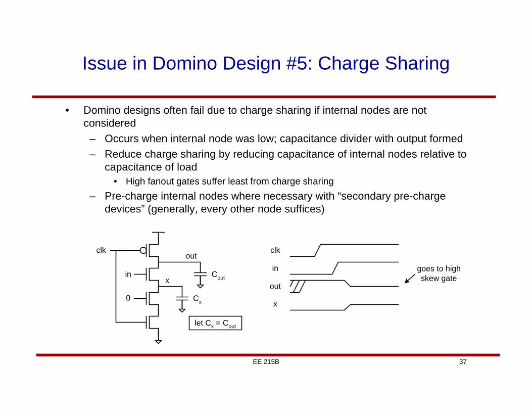
Issue in Domino Design #5: Charge Sharing
• Domino designs often fail due to charge sharing if internal nodes are not considered
– Occurs when internal node was low; capacitance divider with output formed– Reduce charge sharing by reducing capacitance of internal nodes relative to
capacitance of load• High fanout gates suffer least from charge sharing
– Pre-charge internal nodes where necessary with “secondary pre-charge devices” (generally, every other node suffices)
0
in
out
xCout
Cx
let Cx = Cout
out
x
in
clk clk
goes to highskew gate
38EE 215B
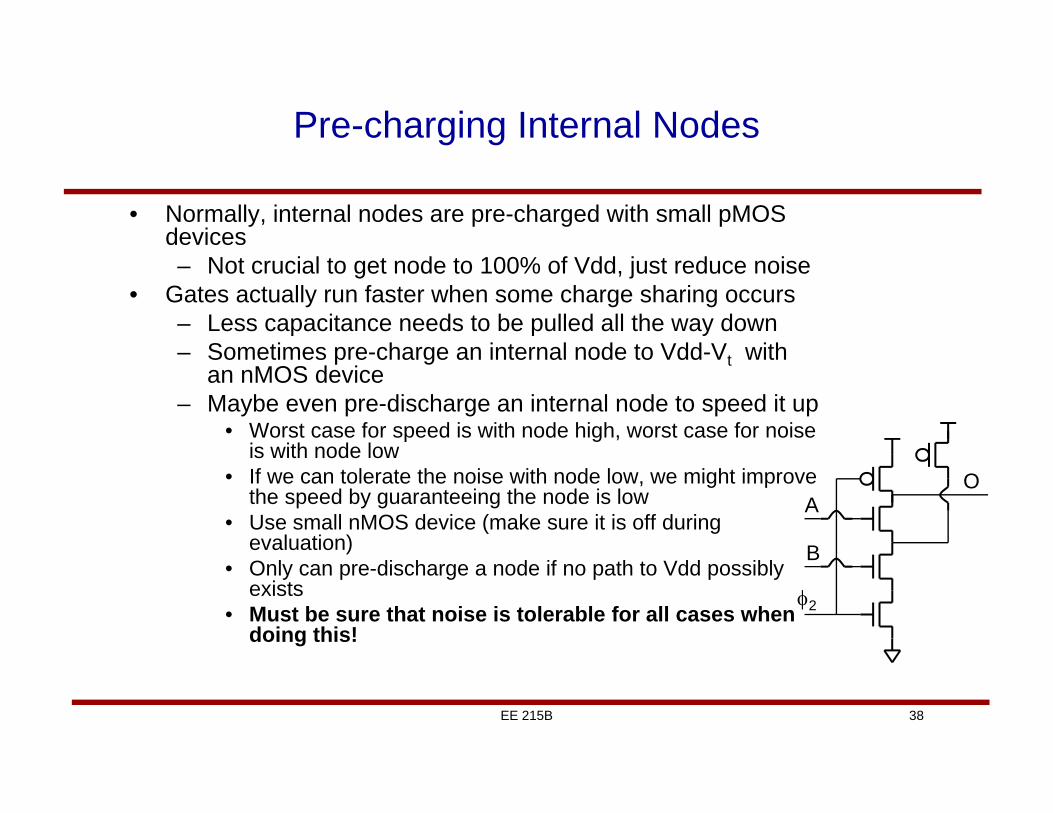
Pre-charging Internal Nodes
• Normally, internal nodes are pre-charged with small pMOS devices– Not crucial to get node to 100% of Vdd, just reduce noise
• Gates actually run faster when some charge sharing occurs– Less capacitance needs to be pulled all the way down– Sometimes pre-charge an internal node to Vdd-Vt with
an nMOS device– Maybe even pre-discharge an internal node to speed it up
• Worst case for speed is with node high, worst case for noise is with node low
• If we can tolerate the noise with node low, we might improve the speed by guaranteeing the node is low
• Use small nMOS device (make sure it is off during evaluation)
• Only can pre-discharge a node if no path to Vdd possibly exists
• Must be sure that noise is tolerable for all cases when doing this!
2
A
B
O
39EE 215B
Domino Pitfalls Review
• There are lots of ways that domino circuits can fail:– Charge sharing and leakage– Noise coupling onto the output (crosstalk).– An -particle hit, sub-threshold leakage, or substrate charge
injection on the dynamic node.– Power supply noise (especially ground bounce).
• Fortunately, these are all relatively easy to check with ERC (Electrical Rule Check) and DRC (Design Rule Check) tools.– Microprocessor companies routinely build reliable domino
datapaths these days.
40EE 215B
Domino Logic Family Outline
• Dynamic/domino logic– Domino logic– Timing of domino logic– Noise issues and keepers
• Dual-rail domino logic (Dynamic CVSL) and other domino styles
41EE 215B
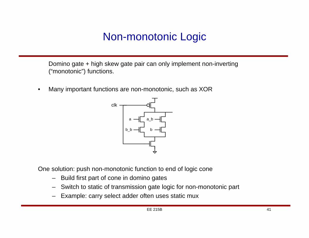
Non-monotonic Logic
clk
a
bb_b
a_b
One solution: push non-monotonic function to end of logic cone– Build first part of cone in domino gates– Switch to static of transmission gate logic for non-monotonic part– Example: carry select adder often uses static mux
Domino gate + high skew gate pair can only implement non-inverting (“monotonic”) functions.
• Many important functions are non-monotonic, such as XOR
42EE 215B
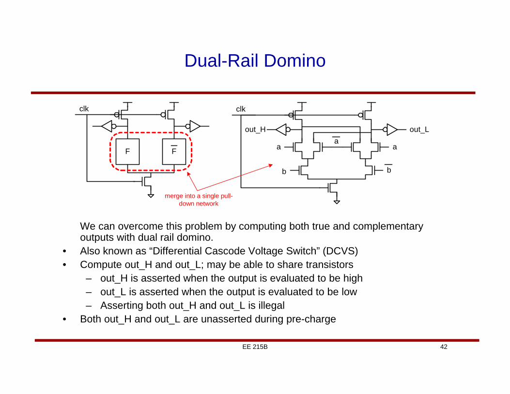
Dual-Rail Domino
aaa
b b
clk
out_L
F
clk
out_H
F
merge into a single pull-down network
We can overcome this problem by computing both true and complementary outputs with dual rail domino.
• Also known as “Differential Cascode Voltage Switch” (DCVS)• Compute out_H and out_L; may be able to share transistors
– out_H is asserted when the output is evaluated to be high– out_L is asserted when the output is evaluated to be low – Asserting both out_H and out_L is illegal
• Both out_H and out_L are unasserted during pre-charge
43EE 215B
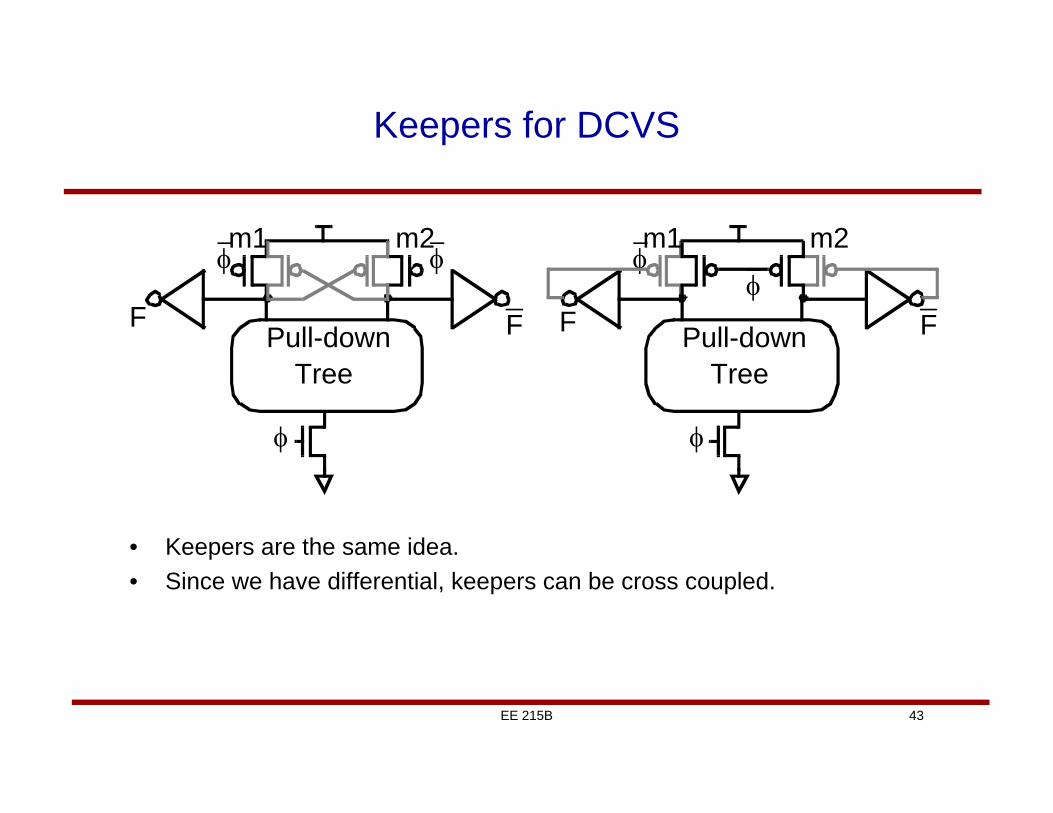
Keepers for DCVS
Pull-downTree
F F
m1 m2
Pull-downTree
F F
m1 m2
• Keepers are the same idea. • Since we have differential, keepers can be cross coupled.
44EE 215B
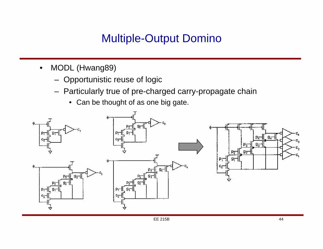
Multiple-Output Domino
• MODL (Hwang89)– Opportunistic reuse of logic– Particularly true of pre-charged carry-propagate chain
• Can be thought of as one big gate.
45
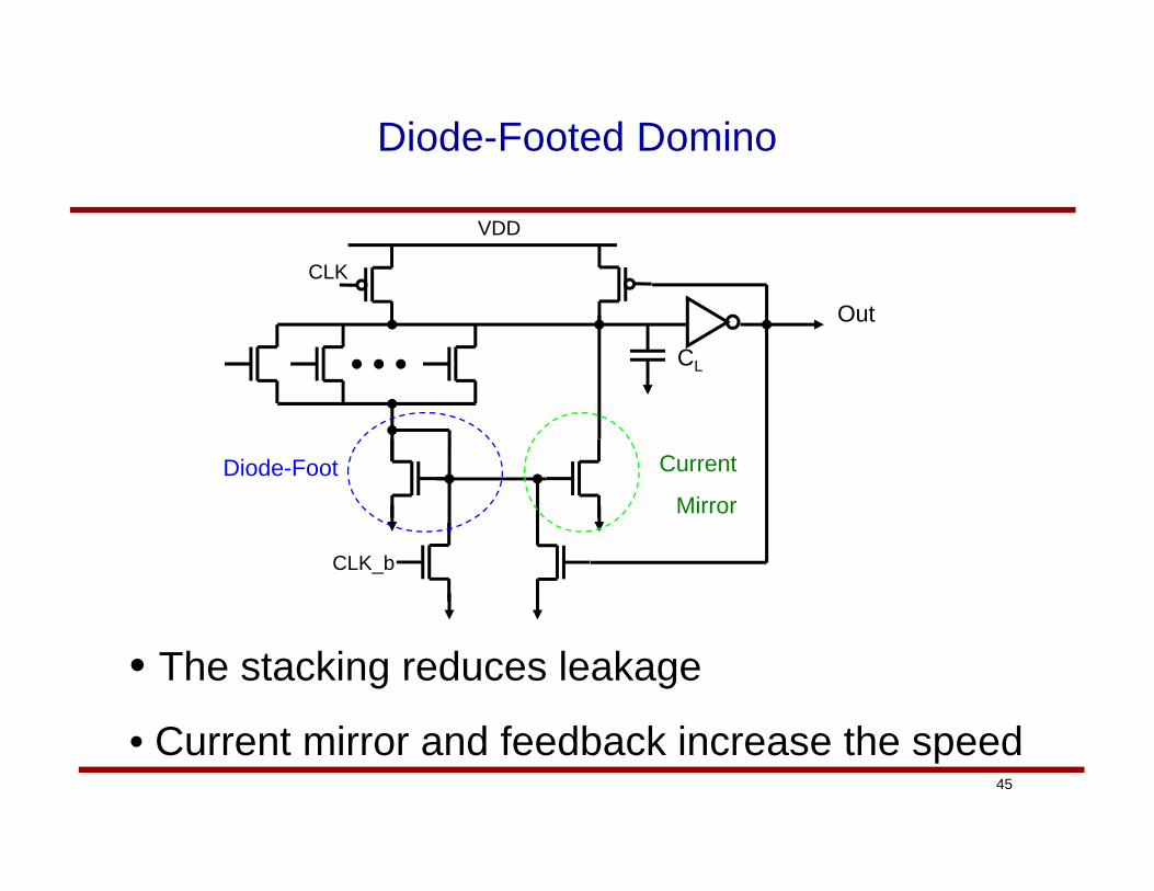
Diode-Footed Domino
VDD
CL
CLK_b
Out
Diode-Foot
CLK
Current
Mirror
• The stacking reduces leakage
• Current mirror and feedback increase the speed
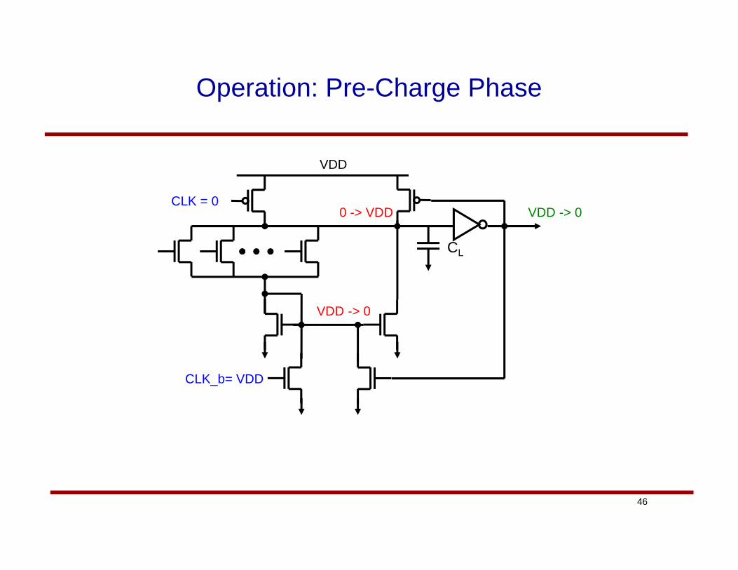
46
Operation: Pre-Charge Phase
VDD
CL
CLK_b= VDD
CLK = 0
VDD -> 0
0 -> VDD VDD -> 0
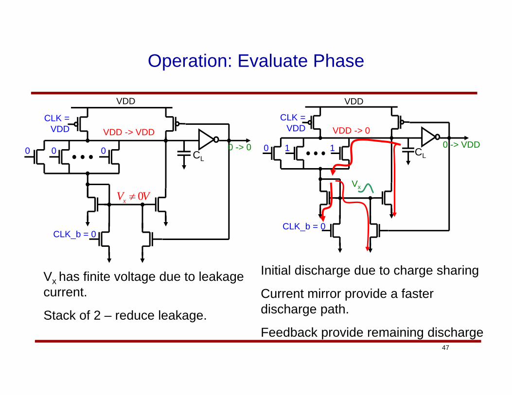
47
Operation: Evaluate Phase
VDD
CL
CLK_b = 0
CLK = VDD VDD -> VDD
0 -> 00 0 0
0xV V
Vx has finite voltage due to leakage current.
Stack of 2 – reduce leakage.
VDD
CL
CLK_b = 0
CLK = VDD VDD -> 0
0 -> VDD0 1 1
Vx
Initial discharge due to charge sharing
Current mirror provide a faster discharge path.
Feedback provide remaining discharge
48
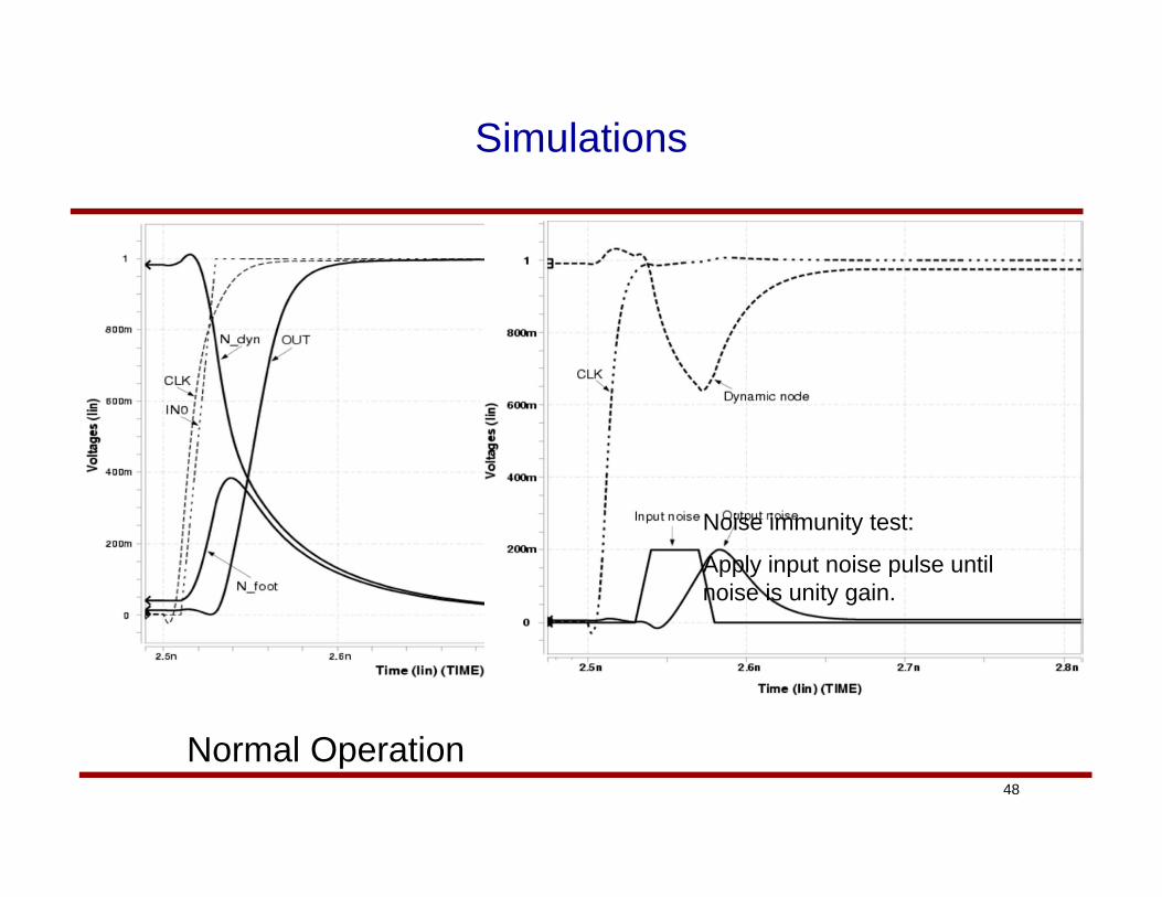
Simulations
Noise immunity test:
Apply input noise pulse until noise is unity gain.
Normal Operation
49
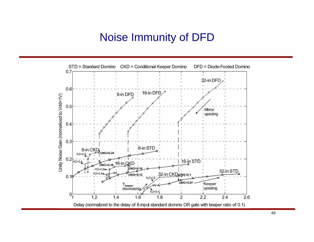
Noise Immunity of DFD
50
Summary
• Dynamic logic is based on optimizing for one edge of evaluation. – To eliminate the other edge, a pre-charge phase is
introduced.• Timing is a critical element of the design• Because one of the nodes is dynamic, noise is another critical
design constraint.– Large internal capacitance can lead to a bad delay-
robustness tradeoff.• Large fanin can be challenging (especially ANDs).
– Monotonicity forces us to build dual rail making ANDs unavoidable.
• Diode-footed is one attempt at pushing the tradeoff to a different point. (We’ll see many more).
EE 215B