Dynamic Logic and Latches II - Stanford...
19
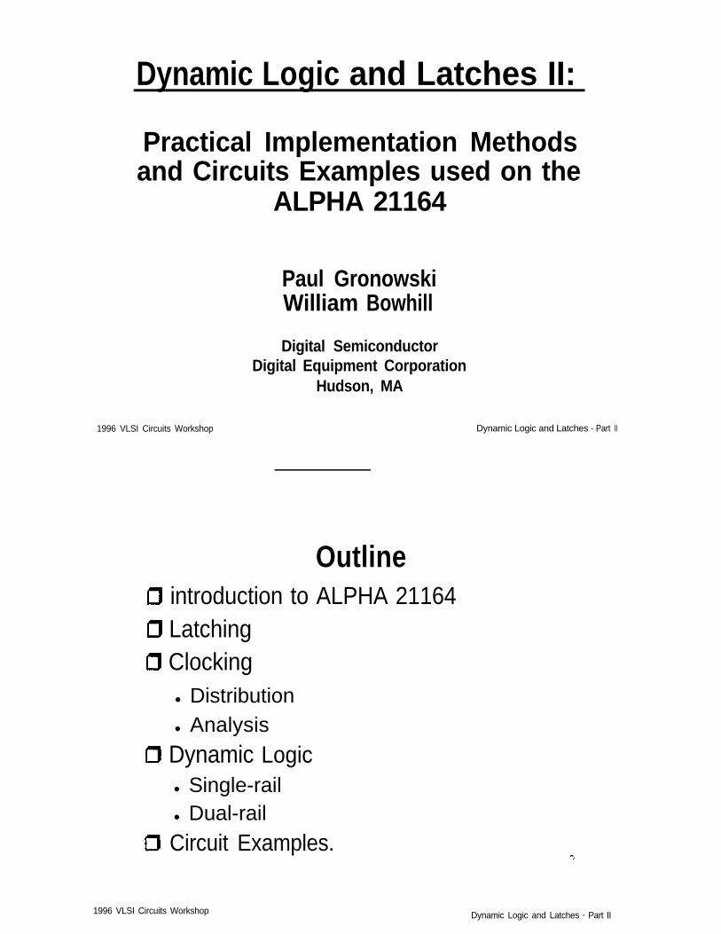
Dynamic Logic and Latches II: Practical Implementation Methods and Circuits Examples used on the ALPHA 21164 Paul Gronowski William Bowhill Digital Semiconductor Digital Equipment Corporation Hudson, MA 1996 VLSI Circuits Workshop Dynamic Logic and Latches - Part II Outline introduction to ALPHA 21164 Latching Clocking l Distribution l Analysis Dynamic Logic l Single-rail l Dual-rail Circuit Examples. 1996 VLSI Circuits Workshop Dynamic Logic and Latches - Part II
Transcript of Dynamic Logic and Latches II - Stanford...
Dynamic Logi c and Latches II:
Practical Implementation Methodsand Circuits Examples used on the
ALPHA 21164
Paul GronowskiWillia m Bowhill
Digital SemiconductorDigital Equipment Corporation
Hudson, MA
1996 VLSI Circuits Workshop Dynamic Logic and Latches - Part II
Outline introduction to ALPHA 21164 Latching Clockingl Distributionl Analysis
Dynamic Logicl Single-raill Dual-rail
Circuit Examples.
1996 VLSI Circuits Workshop Dynamic Logic and Latches - Part II
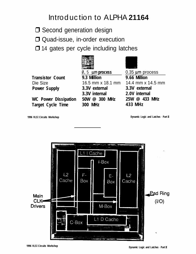
Introduction to ALPHA 21164
Second generation design Quad-issue, in-order execution 14 gates per cycle including latches
0.5 processTransistor Count 9.3 MillionDie Size 16.5 mm x 18.1 mmPower Supply 3.3V external
3.3V internalWC Power Dissipation 50W @ 300 MHzTarget Cycle Time 300 MHz
0.35 process9.66 Million14.4 mm x 14.5 mm3.3V external2.0V internal25W @ 433 MHz433 MHz
1996 VLSI Circuits Workshop Dynamic Logic and Latches - Part II
1996 VLSI Circuits Workshop Dynamic Logic and Latches - Part II
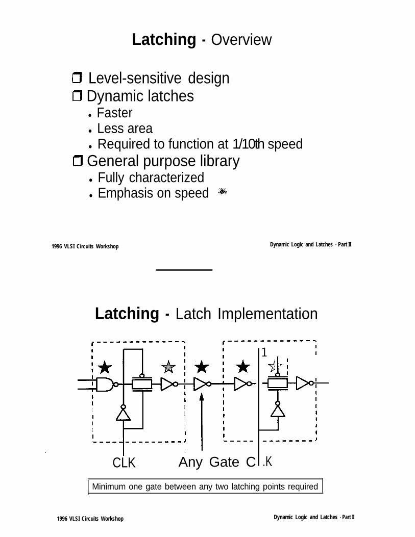
Latching - Overview
Level-sensitive design Dynamic latchesl Fasterl Less areal Required to function at 1/10th speed
General purpose libraryl Fully characterizedl Emphasis on speed
1996 VLSI Circuits Workshop Dynamic Logic and Latches - Part II
Latching - Latch Implementation
I I II
II I
II
1
CLK Any Gate C .K
Minimum one gate between any two latching points required
1996 VLSI Circuits Workshop Dynamic Logic and Latches - Part II
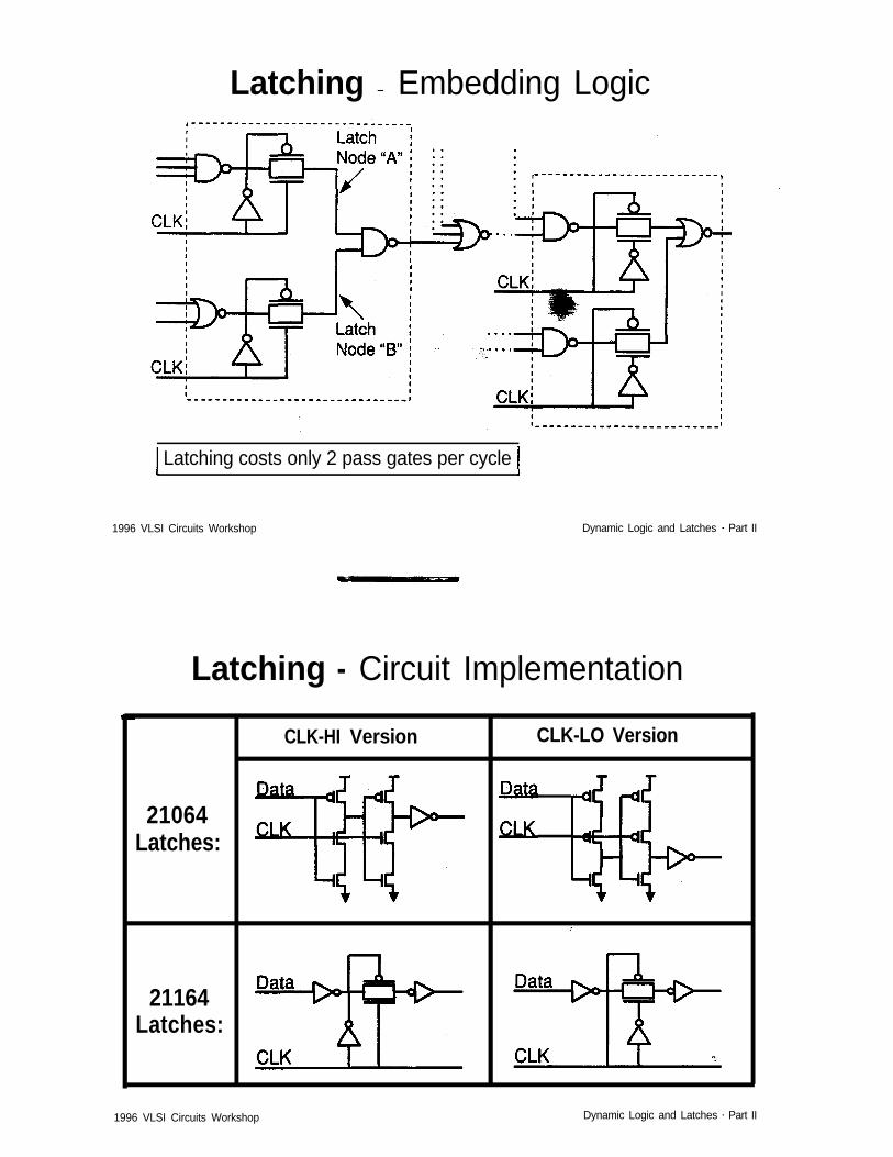
Latching - Embedding Logic
1996 VLSI Circuits Workshop
Latching costs only 2 pass gates per cycle
Dynamic Logic and Latches - Part II
Latching - Circuit Implementation
CLK-HI Version CLK-LO Version
21064Latches:
21164Latches:
1996 VLSI Circuits Workshop Dynamic Logic and Latches - Part II
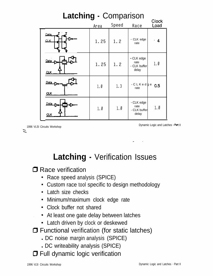
Latching - ComparisonArea Speed Race
1.25 1.2 CLK edgerate
,
CLK edge
1.25 1.2rate
CLK buffer 1.0delay
Da
CLK
1.0 1.3 - C L K e d g e rate
Data
CLK
1996 VLSI Circuits Workshop
1.0 CLK edge
1.0 rate CLK buffer 1.0
delay
Dynamic Logic and Latches II
Latching - Verification Issues
Race verification
Race speed analysis (SPICE)Custom race tool specific to design methodologyLatch size checksMinimum/maximum clock edge rateClock buffer not sharedAt least one gate delay between latchesLatch driven by clock or deskewed
Functional verification (for static latches) l DC noise margin analysis (SPICE)l DC writeability analysis (SPICE)
Full dynamic logic verification
1996 VLSI Circuits Workshop Dynamic Logic and Latches - Part II
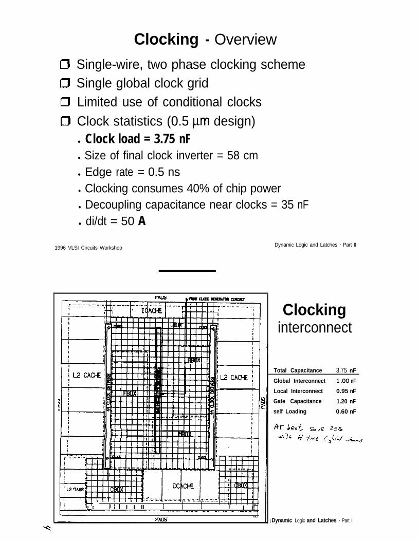
Clocking - Overview
Single-wire, two phase clocking schemeSingle global clock gridLimited use of conditional clocksClock statistics (0.5 design)l Clock load = 3.75 nFl Size of final clock inverter = 58 cml Edge rate = 0.5 nsl Clocking consumes 40% of chip powerl Decoupling capacitance near clocks = 35 nFl di/dt = 50 A
1996 VLSI Circuits Workshop Dynamic Logic and Latches - Part II
y- CACHE
Iii
ii
ii
I I II I I I i I I!
Clockinginterconnect
Total Capacitance 3.75 nF
Global Interconnect 1 .OO nF
Local Interconnect 0.95 nF
Gate Capacitance 1.20 nF
self Loading 0.60 nF
Dynamic Logic and Latches - Part II
CLOCK>>
FROM GENERATOR CIRCUITi
PRE-CLK i
i
i
iI
ii
ii
i
i
CLOCK
ii!
i! ii! ii !i! i! ii! ii !i! ii! ii! i !
i !i !
ii
i !i! ii! i
i! i! ii!
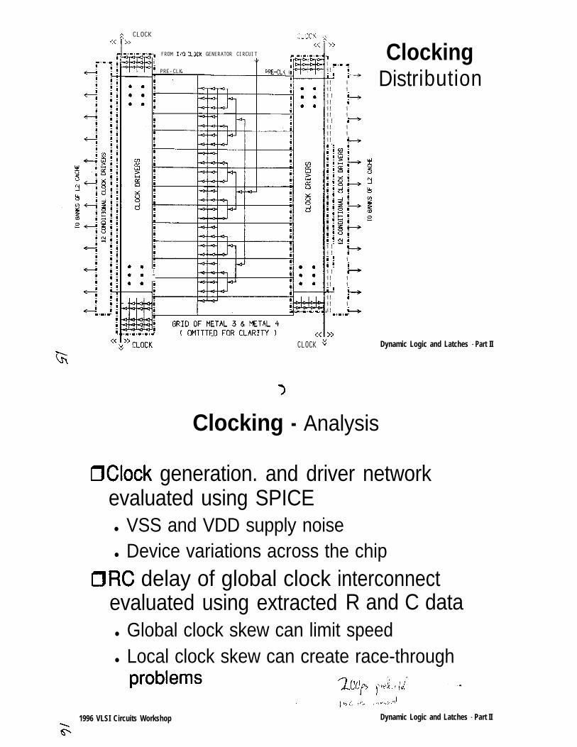
ClockingDistribution
Dynamic Logic and Latches - Part II
Clocking - Analysis
generation. and driver networkevaluated using SPICEl VSS and VDD supply noisel Device variations across the chip
delay of global clock interconnectevaluated using extracted R and C datal Global clock skew can limit speedl Local clock skew can create race-through
1996 VLSI Circuits Workshop Dynamic Logic and Latches - Part II
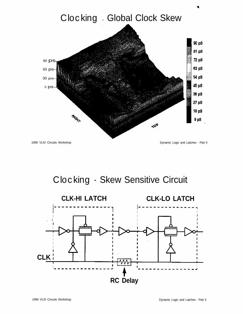
Clocking - Global Clock Skew
90 ps
60 ps-
30 ps-
0 ps-
1996 VLSI Circuits Workshop Dynamic Logic and Latches - Part II
Clocking - Skew Sensitive Circuit
CLK-HI LATCH CLK-LO LATCHI II I I I
I I I
. I I I
I I
I
IIII
CLK I I
RC Delay
1996 VLSI Circuits Workshop Dynamic Logic and Latches - Part II
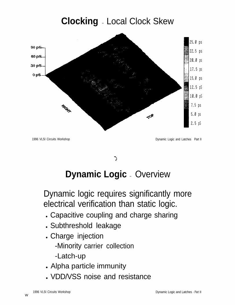
Clocking - Local Clock Skew
25.0 ps
22.5 ps
20.0 ps
17.5 ps
15.0 ps
12.5 pS
10.0 pS
7.5 ps
5.0 ps
2.5 pS
1996 VLSI Circuits Workshop Dynamic Logic and Latches Part II
Dynamic Logic - Overview
Dynamic logic requires significantly moreelectrical verification than static logic.l Capacitive coupling and charge sharingl Subthreshold leakagel Charge injection
-Minority carrier collection-Latch-up
l Alpha particle immunity
l VDD/VSS noise and resistance
1996 VLSI Circuits WorkshopW
Dynamic Logic and Latches - Part II

vss ATDRIVER
Dynamic Logic - Circuit Diagram
COUPLING TODYNAMIC N
OUT
IN_L
COUPLlNG T O
‘LEAK I
RECEIVER
1996 VLSI Circuits Workshop Dynamic Logic and Latches - Part II
Dynamic Logic - General Rules
Dynamic logic can only be driven bycomplementary gates
Complementary gates must be close todynamic structurel Global nodes received by gates with standard
ratio (noise margin)l Local nodes can be received by gates with a
skewed ratio (for speed)
Precharge controlled by clockl Delayed precharge not typically usedl Domino or ripple precharge not typically used
1996 VLSI Circuits Workshop Dynamic Logic and Latches - Part II
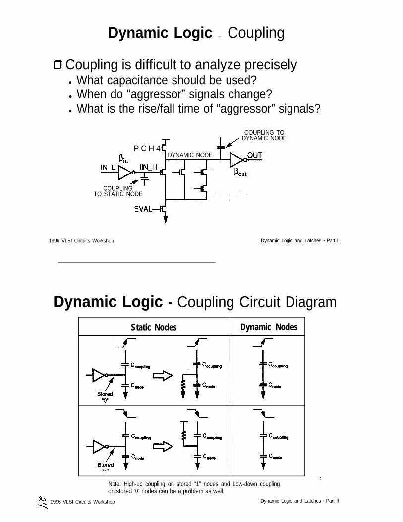
Dynamic Logic - Coupling
Coupling is difficult to analyze preciselyl What capacitance should be used?l When do “aggressor” signals change?l What is the rise/fall time of “aggressor” signals?
COUPLING TODYNAMIC NODE
P C H 4
DYNAMIC NODE
COUPLINGTO STATIC NODE
1996 VLSI Circuits Workshop Dynamic Logic and Latches - Part II
Dynamic Logic - Coupling Circuit Diagram
Static Nodes Dynamic Nodes
Note: High-up coupling on stored “1” nodes and Low-down couplingon stored “0” nodes can be a problem as well.
1996 VLSI Circuits Workshop Dynamic Logic and Latches - Part II
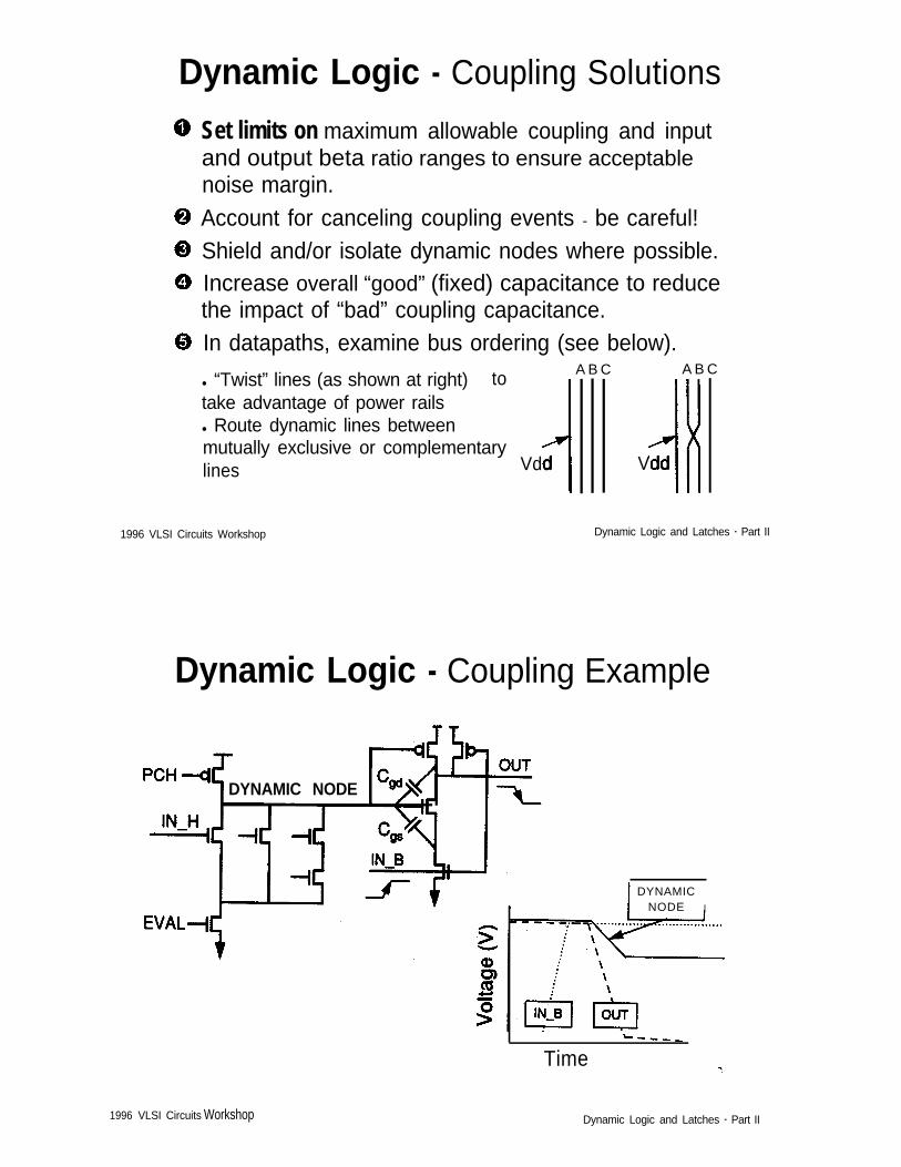
Dynamic Logic - Coupling Solutions
Set limits on maximum allowable coupling and inputand output beta ratio ranges to ensure acceptablenoise margin.Account for canceling coupling events - be careful!Shield and/or isolate dynamic nodes where possible.Increase overall “good” (fixed) capacitance to reducethe impact of “bad” coupling capacitance.In datapaths, examine bus ordering (see below).
l “Twist” lines (as shown at right) to A B C A B C
take advantage of power railsl Route dynamic lines betweenmutually exclusive or complementarylines
Vdd Vdd
1996 VLSI Circuits Workshop Dynamic Logic and Latches - Part II
Dynamic Logic - Coupling Example
DYNAMIC NODE
DYNAMICNODE I
Time
1996 VLSI Circuits Workshop Dynamic Logic and Latches - Part II
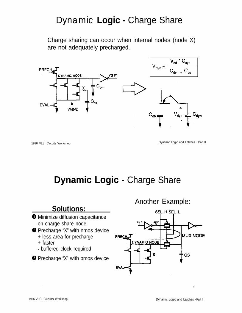
Dynamic Logic - Charge Share
Charge sharing can occur when internal nodes (node X)are not adequately precharged.
V
dyn +
1996 VLSI Circuits Workshop Dynamic Logic and Latches - Part II
Dynamic Logic - Charge Share
Solutions: Minimize diffusion capacitanceon charge share node
Precharge “X” with nmos device+ less area for precharge+ faster
Another Example:
- buffered clock required
Precharge “X” with pmos device
1996 VLSI Circuits Workshop Dynamic Logic and Latches - Part II
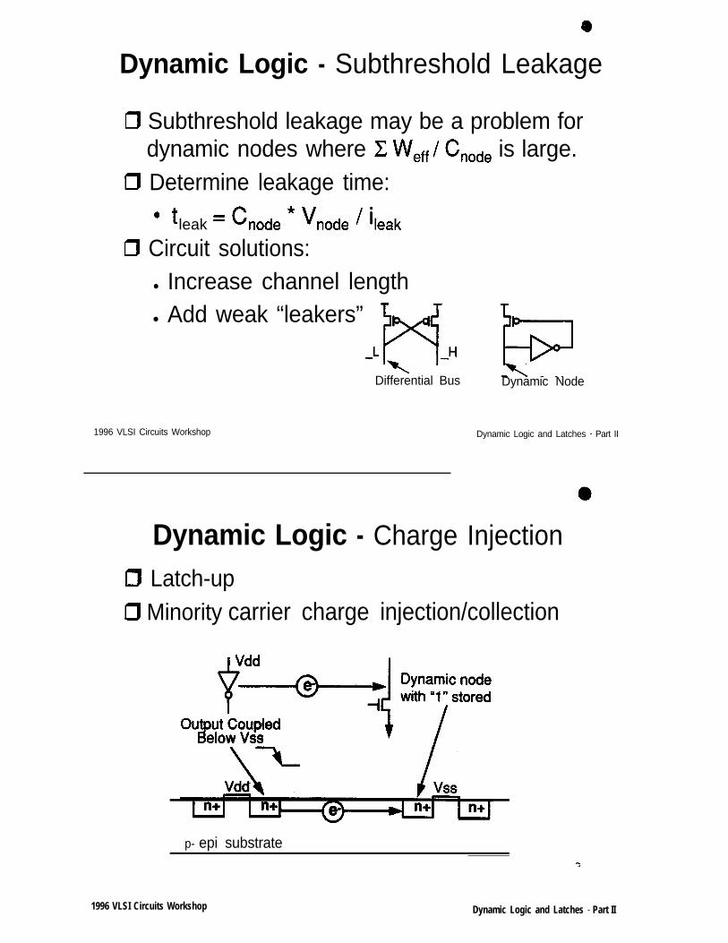
Dynamic Logic - Subthreshold Leakage
Subthreshold leakage may be a problem fordynamic nodes where is large.
Determine leakage time:
leak
Circuit solutions:l Increase channel lengthl Add weak “leakers”
Differential Bus
1996 VLSI Circuits Workshop
Dynamic Node
Dynamic Logic and Latches - Part II
Dynamic Logic - Charge Injection
Latch-up Minority carrier charge injection/collection
p- epi substrate
1996 VLSI Circuits Workshop Dynamic Logic and Latches - Part II
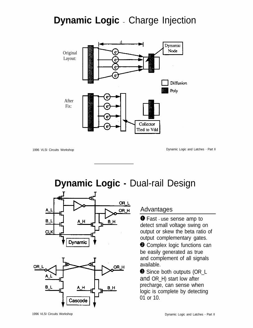
Dynamic Logic - Charge Injection
OriginalLayout:
AfterFix:
1996 VLSI Circuits Workshop Dynamic Logic and Latches - Part II
Dynamic Logic - Dual-rail Design
Advantages Fast - use sense amp to
detect small voltage swing onoutput or skew the beta ratio ofoutput complementary gates.
Complex logic functions canbe easily generated as trueand complement of all signalsavailable.
Since both outputs (OR_Land OR_H) start low afterprecharge, can sense whenlogic is complete by detecting01 or 10.
1996 VLSI Circuits Workshop Dynamic Logic and Latches - Part II
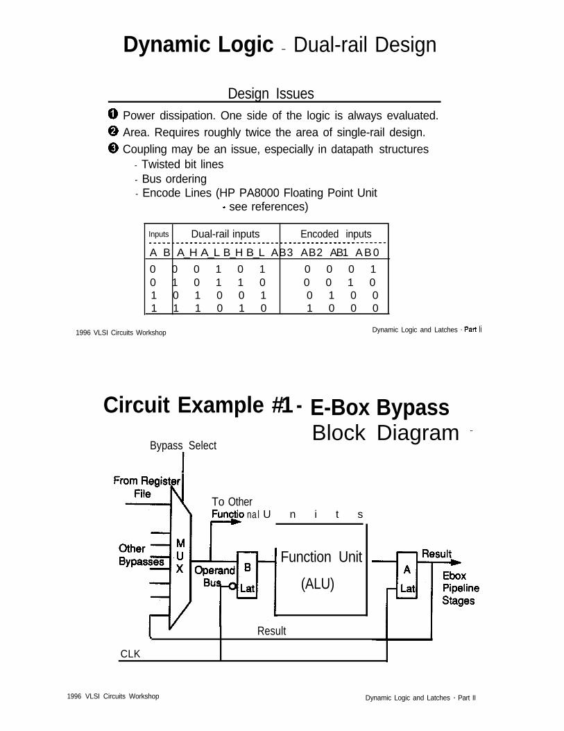
Dynamic Logic - Dual-rail Design
Design Issues Power dissipation. One side of the logic is always evaluated. Area. Requires roughly twice the area of single-rail design. Coupling may be an issue, especially in datapath structures
- Twisted bit lines- Bus ordering- Encode Lines (HP PA8000 Floating Point Unit
see references)
Inputs Dual-rail inputs Encoded inputs
A B A_H A_L B_H B_L AB3 AB2 AB1 A B 0
0 0 0 1 0 1 0 0 0 10 1 0 1 1 0 0 0 1 01 0 1 0 0 1 0 1 0 01 1 1 0 1 0 1 0 0 0
1996 VLSI Circuits Workshop
Circuit Example #1 -
Bypass Select
Dynamic Logic and Latches - Ii
E-Box BypassBlock Diagram
To Other nal U n i t s
Function Unit
(ALU)
Result
CLK
1996 VLSI Circuits Workshop Dynamic Logic and Latches - Part II
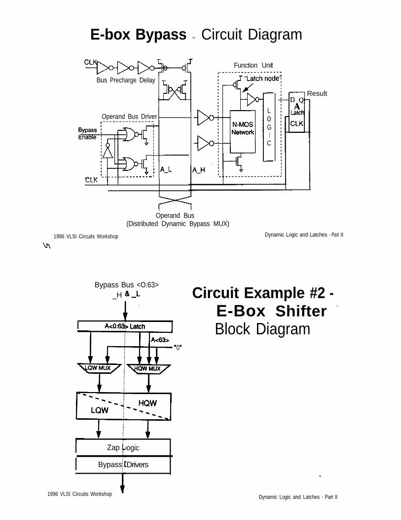
E-box Bypass - Circuit Diagram
Function Unit
Bus Precharge Delay
Result
L0G
IC
Operand Bus Driver
Bypass na e
CLK
Operand Bus(Distributed Dynamic Bypass MUX)
1996 VLSI Circuits Workshop Dynamic Logic and Latches - Part II
Circuit Example #2 -Bypass Bus <O:63>
_H
E-Box Shifter Block Diagram
0
Zap ogic
Bypass Drivers
Dynamic Logic and Latches - Part II 1996 VLSI Circuits Workshop
l
1996 VLSI Circuits Workshop Dynamic Logic and Latches - Part II
l
References“A Dual-Execution Pipelined Floating-Point CMOS Processor”
l
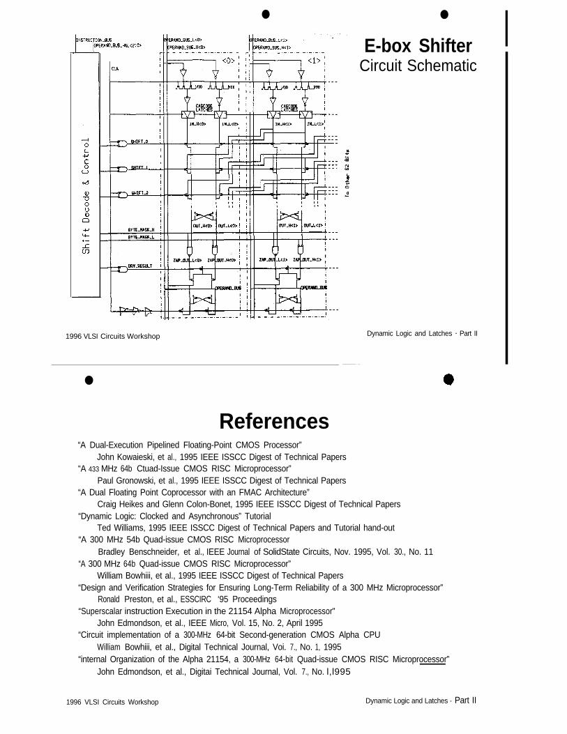
E-box ShifterCircuit Schematic
John Kowaieski, et al., 1995 IEEE ISSCC Digest of Technical Papers“A 433 MHz 64b Ctuad-Issue CMOS RISC Microprocessor”
Paul Gronowski, et al., 1995 IEEE ISSCC Digest of Technical Papers“A Dual Floating Point Coprocessor with an FMAC Architecture”
Craig Heikes and Glenn Colon-Bonet, 1995 IEEE ISSCC Digest of Technical Papers“Dynamic Logic: Clocked and Asynchronous” Tutorial
Ted Williams, 1995 IEEE ISSCC Digest of Technical Papers and Tutorial hand-out“A 300 MHz 54b Quad-issue CMOS RISC Microprocessor
Bradley Benschneider, et al., IEEE Journal of SolidState Circuits, Nov. 1995, Vol. 30., No. 11“A 300 MHz 64b Quad-issue CMOS RISC Microprocessor”
William Bowhiii, et al., 1995 IEEE ISSCC Digest of Technical Papers“Design and Verification Strategies for Ensuring Long-Term Reliability of a 300 MHz Microprocessor”
Ronald Preston, et al., ESSCIRC ‘95 Proceedings“Superscalar instruction Execution in the 21154 Alpha Microprocessor"
John Edmondson, et al., IEEE Micro, Vol. 15, No. 2, April 1995“Circuit implementation of a 300-MHz 64-bit Second-generation CMOS Alpha CPU
William Bowhiii, et al., Digital Technical Journal, Voi. 7., No. 1, 1995“internal Organization of the Alpha 21154, a 300-MHz 64-bit Quad-issue CMOS RISC Microprocessor”
John Edmondson, et al., Digitai Technical Journal, Vol. 7., No. l,l995
1996 VLSI Circuits Workshop Dynamic Logic and Latches - Part II
More References
“Impact of Clock Slope on True Single Phase Clocked (TSPC) CMOS Circuits”Patrik Larsson and Christer Svensson, IEEE Journal of Solid-State Circuits, June 1994, Vol. 29, No. 6
“Noise in Digital Dynamic CMOS Circuits”
Patrik Larsson and Christer Svensson, IEEE Journal of Solid-State Circuits, June 1994, Vol. 29, No. 6“A Comparison of CMOS Circuit Techniques: Differential Cascade Voltage Switch Logic VersusConventional Logic”
Kan M. Chu and David L. Pulfrey, IEEE Journal of Solid-State Circuits, Aug. 1987, Vol. SC-22, No. 4“Design Procedures for Differential Cascade Voltage Switch Circuits”
Kan M. Chu and David L. Pulfrey, IEEE Journal of Solid-State Circuits, Dec. 1986, Vol. SC-21, No. 6‘Clocking Schemes for High-Speed Digital Systems”
Stephen H. Unger, Chung-Jen Tan, IEEE Transactions on Computers, Oct. 1986, Vol. C-35, No. 10“Custom and Semi-Custom Design Techniques”
Lawrence G. Heller, et al., 1984 IEEE ISSCC Digest of Technical Papers“NORA: A Racefree Dynamic CMOS Technique for Pipelined Logic Structures”
Nelson F. Goncalves and Hugo J. De Man, IEEE Journal of Solid-State Circuits, June 1983,Vol. SC-18, No. 3
“High-Speed Compact Circuits with CMOS”R. H. Krambeck, et al., IEEE Journal of Solid-State Circuits, June 1982, Vol. SC-1 7, No. 3
1996 VLSI Circuits Workshop Dynamic Logic and Latches - Part II