DYE-SENSITIZED SOLAR CELLS ON ALTERNATIVE...
73
TKK Dissertations 214 Espoo 2010 DYE-SENSITIZED SOLAR CELLS ON ALTERNATIVE SUBSTRATES Doctoral Dissertation Minna Toivola Aalto University School of Science and Technology Faculty of Information and Natural Sciences Department of Applied Physics
Transcript of DYE-SENSITIZED SOLAR CELLS ON ALTERNATIVE...

TKK Dissertations 214Espoo 2010
DYE-SENSITIZED SOLAR CELLS ON ALTERNATIVE SUBSTRATESDoctoral Dissertation
Minna Toivola
Aalto University School of Science and TechnologyFaculty of Information and Natural SciencesDepartment of Applied Physics


TKK Dissertations 214Espoo 2010
DYE-SENSITIZED SOLAR CELLS ON ALTERNATIVE SUBSTRATESDoctoral Dissertation
Minna Toivola
Doctoral dissertation for the degree of Doctor of Science in Technology to be presented with due permission of the Faculty of Information and Natural Sciences for public examination and debate in Auditorium K216 at the Aalto University School of Science and Technology (Espoo, Finland) on the 16th of April 2010 at 12 noon.
Aalto University School of Science and TechnologyFaculty of Information and Natural SciencesDepartment of Applied Physics
Aalto-yliopistoTeknillinen korkeakouluInformaatio- ja luonnontieteiden tiedekuntaTeknillisen fysiikan laitos

Distribution:Aalto UniversitySchool of Science and TechnologyFaculty of Information and Natural SciencesDepartment of Applied PhysicsP.O. Box 14100FI - 00076 AaltoFINLANDURL: http://tfy.tkk.fi/Tel. +358-9-470 23198Fax +358-9-470 23195E-mail: [email protected]
© 2010 Minna Toivola
ISBN 978-952-60-3069-2ISBN 978-952-60-3070-8 (PDF)ISSN 1795-2239ISSN 1795-4584 (PDF)URL: http://lib.tkk.fi/Diss/2010/isbn9789526030708/
TKK-DISS-2734
Aalto-PrintHelsinki 2010

ABSTRACT OF DOCTORAL DISSERTATION AALTO UNIVERSITY SCHOOL OF SCIENCE AND TECHNOLOGY P.O. BOX 11000, FI-00076 AALTO http://www.aalto.fi
Author Minna Toivola
Name of the dissertation
Dye-sensitized solar cells on alternative substrates
Manuscript submitted 29.10.2009 Manuscript revised 8.2.2010
Date of the defence 16.4.2010
Monograph Article dissertation (summary + original articles)
Faculty Faculty of Information and Natural Sciences
Department Department of Applied Physics
Field of research New Energy Technologies
Opponent(s) Prof. Michael Grätzel
Supervisor Prof. Peter Lund
Instructor Prof. Peter Lund
Abstract
Dye-sensitized solar cells (DSC) could become a potential alternative for the traditional silicon and thin film panels in the near future,
due to the DSC’s for the most part cheap materials and simple manufacturing methods. One of the challenges of this technology is,
however, the heavy, expensive and inflexible glass substrate typically used in the cells. To address this problem, this thesis concentrates
on transfer of the DSC technology from glass substrates to light weight, cost-efficient, and flexible plastic foils and metal sheets. Flexible
solar cell would be well suited for industrial-scale mass production, for example with roll-to-roll methods and when integrated on
building materials it could work as a functional coating, enabling electricity-producing roofing or façade structures.
In the course of this thesis, DSCs were prepared on ITO-PET and ITO-PEN plastics, stainless steel (StS), and optical fibers. Due to the
low temperature tolerance of the plastics, development and characterization of room temperature processable counter electrode materials
suitable for these substrates was a part of this work. Powder suspension based on carbon nanoparticles proved to be an easily depositable,
cost-efficient material with catalytic activity as high as that of platinum. With metal materials, the main problem is the corrosive, iodine-
based electrolyte conventionally used in the DSC. This is why, in the beginning of this work, the corrosion resistance of some widely
used building materials such as zinc-coated carbon steels, copper, and StS was studied with soaking tests in the electrolyte. StS passed
the soaking tests and was chosen for further research. StS has also other benefits such as good electrical conductivity and mechanical
sturdiness. Substrate-mediated leakage current is also smaller from StS than from glass substrates. With a DSC configuration where the
StS sheet worked as the photoelectrode substrate efficiencies comparable to all-glass cells, near 5 %, were obtained so this configuration
was chosen also for the cell size upscaling tests. The largest StS photoelectrode cells prepared in the course of this thesis were 6 cm x 6
cm and their efficiencies over 3 % at their best. This is already a promising value considering the ohmic losses bound to happen at the
counter electrode, due to the sheet resistance of the counter electrode substrate. To minimize these losses, additional current collector
structures were integrated on the counter electrode substrate with inkjet-printing with silver nanoparticle ink. 50 % reduction in the total
ohmic losses of the cell was achieved with the current collector structures and 80 % with replacing the photoelectrode glass substrate
with the StS sheet.
StS-based DSC would seem like a feasible concept even for industrial-scale mass production but special emphasis should be put, in the
future research, on the long term stability of the cells and its improvement. Room for improvement still exists in efficiencies also – a
research challenge in which for example some recently developed carbon nanomaterials might provide progress.
Keywords dye solar cell, plastic substrate, metal substrate, nanomaterials
ISBN (printed) 978-952-60-3069-2 ISSN (printed) 1795-2239
ISBN (pdf) 978-952-60-3070-8 ISSN (pdf) 1795-4584
Language English Number of pages 64 p. + app. 91 p.
Publisher Aalto University School of Science and Technology
Print distribution Department of Applied Physics
The dissertation can be read at http://lib.tkk.fi/Diss/2010/isbn9789526030708/


VÄITÖSKIRJAN TIIVISTELMÄ AALTO-YLIOPISTO TEKNILLINEN KORKEAKOULU PL 11000, 00076 AALTO http://www.aalto.fi
Tekijä Minna Toivola
Väitöskirjan nimi
Väriaineherkistetyt aurinkokennot vaihtoehtoisilla alustoilla
Käsikirjoituksen päivämäärä 29.10.2009 Korjatun käsikirjoituksen päivämäärä 8.2.2010
Väitöstilaisuuden ajankohta 16.4.2010
Monografia Yhdistelmäväitöskirja (yhteenveto + erillisartikkelit)
Tiedekunta Informaatio- ja luonnontieteiden tiedekunta
Laitos Teknillinen fysiikka
Tutkimusala Energiatieteet
Vastaväittäjä(t) Prof. Michael Grätzel
Työn valvoja Prof. Peter Lund
Työn ohjaaja Prof. Peter Lund
Tiivistelmä
Väriaineherkistetyn nanoaurinkokennon suurimmaksi osaksi edullisista valmistusmateriaaleista ja kennon yksinkertaisesta
valmistettavuudesta johtuen tästä teknologiasta ennustetaan lähitulevaisuudessa potentiaalista vaihtoehtoa nyt yleisesti käytössä oleville
pii- ja ohutkalvopaneeleille. Eräs väriaineaurinkokennon ongelmista on kuitenkin raskas, kallis ja joustamaton lasisubstraatti, jolle
kennot on tyypillisesti valmistettu. Tässä työssä onkin tutkittu kuinka kennoteknologia saataisiin siirrettyä lasisubstraateilta kevyille,
taipuisille ja edullisille muovikalvoille ja metallilevyille. Joustava kenno soveltuisi hyvin myös teolliseen massatuotantoon,
valmistettavaksi kelalta-kelalle –menetelmillä. Rakennusmateriaaleihin integroituna se voisi taas toimia funktionaalisena pinnoitteena,
mahdollistaen esim. sähköä tuottavat katto- tai fasadirakenteet.
Tämän työn aikana valmistettiin väriaineaurinkokennoja ITO-PET ja ITO-PEN –muoveille, ruostumattomalle teräkselle (RST) ja
optisille valokuiduille. Koska muovisubstraatit eivät kestä korkeita lämpötiloja, eräs työn osa-alue oli muoveille soveltuvien, huoneen
lämpötilassa prosessoitavien vastaelektrodimateriaalien kehittäminen ja karakterisointi. Hiilinanopartikkelipohjainen pulverisuspensio
osoittautui helposti depositoitavaksi ja edulliseksi materiaaliksi, jonka katalyyttinen aktiivisuus oli parhaimmillaan platinan luokkaa.
Metallimateriaalien käyttöä väriaineaurinkokennossa rajoittaa kennon jodipohjainen elektrolyytti, joka korrondoi monia metalleja. Työn
aluksi selvitettiinkin yleisesti käytettyjen rakennusmetallien sinkityn hiiliteräksen, kuparin ja ruostumattoman teräksen
korroosiokestävyys liuotuskokein elektrolyytissä. RST läpäisi liuotuskokeet ja valittiin näin ollen jatkotutkimuksiin. RST:llä on myös
muita etuja, mm. hyvä sähkönjohtavuus, mekaaninen kestävyys ja pienempi vuotovirta substraatista elektrolyyttiin. RST-
valoelektrodipohjaisella kennokonfiguraatiolla saavutettiinkin lasikennoon verrattava hyötysuhde, lähes 5 %, joten tämä konfiguraatio
valittiin myös kennon koon kasvatuskokeisiin. Suurimmat työn aikana valmistetut RST-valoelektrodikennot olivat kooltaan 6 cm x 6 cm,
ja niiden hyötysuhde parhaimmillaan yli 3 %, mikä on jo lupaava arvo ottaen huomioon mm. vastaelektrodilla tapahtuvat, substraatin
pintavastuksesta johtuvat ohmiset häviöt. Näiden häviöiden minimoimiseksi integroitiin vastaelektrodiin ylimääräiset
virrankeräinrakenteet hopeananopartikkelimusteella mustesuihkutulostustekniikalla. Virrankeräinrakenteilla onnistuttiin pienentämään
kennon kokonaisvastusta 50 % ja korvaamalla valoelektrodin lasisubstraatti RST:llä 80 %.
RST-pohjainen kenno vaikuttaisi toteuttamiskelpoiselta ratkaisulta jopa teollisen mittakaavan massatuotantoon, mutta erityistä huomiota
tulisi jatkotutkimuksissa kehittää sen pitkän ajan stabiilisuuden parantamiseen. Myös hyötysuhdetta tulisi saada nostettua – tässä mm.
hiilinanomateriaalit ovat eräs varteenotettava tutkimuskohde.
Asiasanat Väriaineherkistetty aurinkokenno, muovisubstraatti, metallisubstraatti, nanomateriaalit
ISBN (painettu) 978-952-60-3069-2 ISSN (painettu) 1795-2239
ISBN (pdf) 978-952-60-3070-8 ISSN (pdf) 1795-4584
Kieli Englanti Sivumäärä 64 s. + liit. 91 s.
Julkaisija Aalto-yliopiston teknillinen korkeakoulu
Painetun väitöskirjan jakelu Teknillisen fysiikan laitos
Luettavissa verkossa osoitteessa http://lib.tkk.fi/Diss/2010/isbn9789526030708/


1
Preface
This thesis is based on research carried out at the Helsinki University of Technology (TKK),
Department of Applied Physics, at the New Energy Technologies group (NEW) between years
2004 - 2010. Funding for this work was provided mainly by Finnish Funding Agency for
Technology and Innovation (Tekes) and Academy of Finland. I would also like to thank the
Finnish Foundation for Technology Promotion (TES) for an incentive scholarship and the
National Graduate School of Energy Technology for the travel grants for conference trips.
I thank my supervisor, professor Peter Lund for introducing me to the diverse and dynamic field
of photovoltaics and especially to one of its latest inventions, nanostructured dye solar cell.
Experimenting with this cell type calls for multidisciplinary approach, combining chemistry,
physics and material science. As I came from quite a different field there has been a lot to learn
and the road has been rocky at times but nothing truly valuable in this life comes easily.
What forms the core of an efficient, productive, encouraging, and pleasant workplace are people.
This is why I have immensely enjoyed my years in the NEW group – not only because of the high
academic quality of the research here but because of the friendly, relaxed and helpful working
atmosphere. It was easy to integrate into this group straight from the beginning and there have
been people who became not only workmates at the time but also good friends, expanding my
horizons and introducing me to new and interesting things also outside of the academic world.
My sincere thanks go to my current colleagues Dr. Janne Halme, Dr. Kati Miettunen, Kerttu
Aitola, Suvi Karvonen, Rami Niemi, Imran Asghar, and Ghufran Hashmi, and all Master’s Thesis
and special assignment workers whose work contribution has been an important part of our
research too. And all the former workmates – Dr. Mikko Mikkola, Dr. Petri Konttinen, Dr.
Thomas Carlsson, Dr. Tero Hottinen, Dr. Olli Himanen, Dr. Iwao Nitta, Dr. Jukka Paatero, Dr.
Marju Ferenets from Tampere Technical University, Timo Peltola, Saara Tuurala, Sonja Auvinen,
Timo Lehtinen, Fredrik Ahlskog, Antti Tolvanen, Jaakko Saarinen – it was a pleasure to work
with you. If I forgot someone, my sincere apologies – lots of people come and go in six years.
The international nature of this field, industrial co-operation and possibility to learn not only
scientific but also organizational and teaching skills have also been extremely valuable
dimensions of my job here.
Finally, sincere thanks to my parents, Eila and Kalevi Toivola, for your endless support in
everything I’ve ventured to in my life, and to my friends, for providing pastime and entertainment
definitely non-academic by nature.
Otaniemi, Espoo, February 2010
Minna Toivola

2
Table of contents
Preface................................................................................................................................. 1
Table of contents................................................................................................................. 2
List of Publications ............................................................................................................. 4
Author’s contribution.......................................................................................................... 5
Other publications by the author not included in this thesis............................................... 6
Abbreviations...................................................................................................................... 7
Symbols............................................................................................................................... 8
1 Introduction............................................................................................................... 10
1.1 Background ....................................................................................................... 10
1.2 Objectives of the study...................................................................................... 10
1.3 Thesis outline .................................................................................................... 12
2 Dye-sensitized solar cells (DSC) .............................................................................. 13
2.1 Background, motivation and current status of solar energy utilization ............ 13
2.2 Principles of photovoltaic conversion............................................................... 16
2.3 DSC structure and operating principle.............................................................. 18
2.4 DSC basic materials and manufacturing methods ............................................ 23
2.4.1 Substrates .................................................................................................. 23
2.4.2 Photoelectrode........................................................................................... 23
2.4.3 Electrolyte ................................................................................................. 25
2.4.4 Counter electrode ...................................................................................... 26
2.4.5 Cell assembly............................................................................................ 27
2.5 State of the art in DSC on different substrates.................................................. 27
3 Research methods ..................................................................................................... 30
3.1 Current-voltage curve measurements ............................................................... 30
3.2 Electrochemical impedance spectroscopy ........................................................ 32
4 Experimental work.................................................................................................... 38
4.1 DSC materials and preparation ......................................................................... 38
4.2 Cell characterization – measurements and equipment...................................... 39
5 Results and discussion .............................................................................................. 40
5.1 Low temperature depositable counter electrodes for plastic substrates
(Publication I) ............................................................................................................... 40

3
5.2 Preliminary tests on industrial sheet metals for DSC substrates
(Publication II) .............................................................................................................. 44
5.3 Further studies on the suitability of metal materials for DSC substrates
(Publications V and VII) ............................................................................................... 46
5.4 Upscaling the metal-based DSC
(Publication VI) ............................................................................................................ 48
5.5 Cylindrical DSC structure on optical fiber
(Publication VIII).......................................................................................................... 51
5.6 The effect of temperature variations on the fresh and aged DSC performance
(Publications III and IV) ............................................................................................... 53
6 Summary and conclusions ........................................................................................ 58
References......................................................................................................................... 61

4
List of Publications
I Halme, Janne; Toivola, Minna; Tolvanen, Antti; Lund, Peter, Charge transfer
resistance of spray deposited and compressed counter electrodes for dye-sensitized
nanoparticle solar cells on plastic substrates, Solar Energy Materials and Solar Cells 90,
872-886 (2006). http://dx.doi.org/10.1016/j.solmat.2005.05.007
II Toivola, Minna; Ahlskog, Fredrik; Lund, Peter, Industrial sheet metals for
nanocrystalline dye-sensitized solar cell structures, Solar Energy Materials and Solar
Cells 90, 2881-2893 (2006). http://dx.doi.org/10.1016/j.solmat.2006.05.002
III Toivola, Minna; Peltokorpi, Lauri; Halme, Janne; Lund, Peter, Regenerative
effects by temperature variations in dye-sensitized solar cells, Solar Energy Materials and
Solar Cells 91, 1733-1742 (2007). http://dx.doi.org/10.1016/j.solmat.2007.05.030
IV Toivola, Minna; Halme, Janne; Peltokorpi, Lauri; Lund, Peter, Investigation of
temperature and aging effects in nanostructured dye solar cells studied by
electrochemical impedance spectroscopy, International Journal of Photoenergy 2009,
Article ID 786429 (2009). http://dx.doi.org/10.1155/2009/786429
V Miettunen, Kati; Halme, Janne; Toivola, Minna; Lund, Peter, Initial performance
of dye solar cells on stainless steel substrates, Journal of Physical Chemistry C 112,
4011-4017 (2008). http://dx.doi.org/10.1021/jp7112957
VI Toivola, Minna; Peltola, Timo; Miettunen, Kati; Halme, Janne; Lund, Peter, Thin
film nano solar cells - from device optimization to upscaling, Journal of Nanoscience and
Nanotechnology 10, 1-7 (2010). http://dx.doi.org/10.1166/jnn.2010.1872
VII Toivola, Minna; Miettunen, Kati; Halme, Janne; Lund, Peter, Thin
Nanostructured Solar Cells on Metal Sheets, NSTI Nanotech - The Nanotechnology
Conference and Trade Show, Boston, U.S.A, June 1-5, 2008, Technical Proceedings of
the CTSI Clean Technology and Sustainable Industries Conference and Trade Show, 96-
99 (2008).
VIII Toivola, Minna; Ferenets, Marju; Lund, Peter; Harlin, Ali, Photovoltaic fiber,
Thin Solid Films 517, 2799-2802 (2009). http://dx.doi.org/10.1016/j.tsf.2008.11.057

5
Author’s contribution
I The author conducted the most of the experiments and data analysis and took part
in writing the paper.
II The author planned the research, took part in the sample preparation,
measurements and data analysis and wrote the most of the paper (based on the results
reported in the M.Sc. thesis of Fredrik Ahlskog, which she supervised).
III The author planned the research, took part in the sample preparation,
measurements and data analysis and wrote the most of the paper.
IV The author planned the research, took part in the sample preparation,
measurements and data analysis and wrote the most of the paper.
V The author contributed to discussions about the paper with the co-authors and
commented and proofread the paper, which is direct continuation to the research she
initiated in Publication II.
VI The author planned the research, assisted in the measurements and data analysis
and wrote the most of the paper (based on the results reported in the M.Sc. thesis of Timo
Peltola, which she supervised).
VII The author wrote the most of the paper, which is a summary and overview of her
own and her co-authors’ work, some of which she partially supervised (M.Sc. thesis of
Kati Miettunen).
VIII The author planned the research, developed a new material used in the samples,
was mainly responsible for the sample preparation, measurements and data analysis and
wrote the paper together with Marju Ferenets.

6
Other publications by the author not included in this thesis
Toivola, Minna; Halme, Janne; Miettunen, Kati; Aitola, Kerttu; Lund, Peter, Nanostructured dye
solar cells on flexible substrates - Review, International Journal of Energy Research 33, 1145-
1160 (2009). http://dx.doi.org/10.1002/er.1605
Miettunen, Kati; Halme, Janne; Vahermaa, Paula; Saukkonen, Tapio; Toivola, Minna; Lund,
Peter, Dye solar cells on ITO-PET substrate with TiO2 recombination blocking layers, Journal of
The Electrochemical Society 156, B876-B883 (2009). http://dx.doi.org/10.1149/1.3138129
Miettunen, Kati; Halme, Janne; Saukkonen, Tapio; Peltola, Timo; Toivola, Minna; Lund Peter,
Performance degradation of dye solar cells on flexible stainless steel substrates, 24th European
Photovoltaic Solar Energy Conference, Hamburg, Germany, September 21-25, 2009, Proceedings
of the 24th European Photovoltaic Solar Energy Conference, xxxx-xxxx (2009).
Asghar, Muhammad Imran; Miettunen, Kati; Halme, Janne; Toivola, Minna; Aitola, Kerttu;
Vahermaa, Paula; Lund, Peter, Stability issues of improved dye sensitized solar cells, 24th
European Photovoltaic Solar Energy Conference, Hamburg, Germany, September 21-25, 2009,
Proceedings of the 24th European Photovoltaic Solar Energy Conference, xxxx-xxxx (2009).
Toivola, Minna; Peltola, Timo; Miettunen, Kati; Halme, Janne; Aitola, Kerttu; Lund, Peter, Large
area optimized thin film nano solar cells on metal sheet, NSTI Nanotech – The Nanotechnology
Conference and Trade Show, Houston, U.S.A, May 3-7, 2009, Technical Proceedings of the CTSI
Clean Technology and Sustainable Industries Conference and Trade Show, 126-129 (2009).
Guangseng, Huang; Halme, Janne; Miettunen, Kati; Toivola, Minna; Lund, Peter, The
performance enchancement by back reflection in nanostructured dye-sensitized solar cells, ISES
World Congress 2007, Beijing, China, September 18-21, 2007, Proceedings of the ISES World
Congress, 1055-1058 (2007).
Toivola, Minna; Halme, Janne; Peltokorpi, Lauri; Lund, Peter, Aging and regenerative behavior
through cyclic temperature of nanostructured, dye-sensitized solar cells, 22nd
European
Photovoltaic Solar Energy Conference, Milan, Italy, September 3-7, 2007, Proceedings of the
22nd
European Photovoltaic Solar Energy Conference, 454-460 (2007).
Miettunen, Kati; Toivola, Minna; Halme, Janne; Armentia, Jon; Vahermaa, Paula; Lund, Peter,
Optimization of dye-sensitized solar cells on stainless steel, 22nd
European Photovoltaic Solar
Energy Conference, Milan, Italy, September 3-7, 2007, Proceedings of the 22nd
European
Photovoltaic Solar Energy Conference, 512-515 (2007).
Toivola, Minna; Miettunen, Kati; Halme, Janne; Ahlskog, Fredrik; Lund, Peter, Nanostructured
dye-sensitized solar cells on flexible substrates using industrially scaleable manufacturing
methods, 21st European Photovoltaic Solar Energy Conference, Dresden, Germany, September 4-
8 , 2006, Proceedings of the 21st European Photovoltaic Solar Energy Conference, 47-52 (2006).

7
Abbreviations
AC alternating current
AM 1.5 G incident air mass 1.5 global spectrum
a-Si amorphous silicon
BIPV building-integrated photovoltaics
CE counter electrode
CIGS copper-indium-gallium selenide
CIS copper-indium sulphide
CPE constant phase element
DMPII 1,2-dimethylimidazolium iodide
DSC dye-sensitized solar cell
EIS electrochemical impedance spectroscopy
EPIA European Photovoltaic Industry Association
FTO fluorine-doped tin oxide
HOMO highest occupied molecular orbital
IR infrared
ITO indium-doped tin oxide
LED light-emitting diode
LUMO lowest unoccupied molecular orbital
MePRN 3-methoxypropionitrile
PANI polyaniline
PE photoelectrode
PEDOT poly(3,4-ethylenedioxythiophene)
PEN polyethylenenaphtalate
PET polyethyleneterephtalate
PMII 1-methyl-3-propylimidazolium iodide
PMMA polymethylmethacrylate
PV photovoltaic
PVDF-HFP polyvinylidenefluoride-hexafluoropropylene
spiro-MeOTAD 2,2′7,7′-tetrakis-(N,N-di-p-methoxyphenyl-amine)-9,9′-
spirobifluorene
StS stainless steel
TCO transparent conducting oxide
TL transmission line
UV ultraviolet

8
Symbols
B0 CPE impedance pre-factor
C capacitance
Cce CE capacitance
cI3- triiodide concentration
Cpe PE capacitance
CPEce CPE describing the CE capacitance
CPEco CPE describing the capacitance at the substrate-TiO2 interface
CPEpe CPE describing the PE capacitance
cpepe distributed PE CPE element
CPEsu CPE describing the capacitance at the substrate-electrolyte
interface
d TiO2 film thickness
DI3- triiodide diffusion coefficient
F Faraday’s constant
f frequency
f* characteristic frequency
FF fill factor
h Planck’s constant
IAC AC current signal in EIS
Id diode current
ilim diffusion-limited current density
Impp current at maximum power point
Iph photogenerated current
Iref,sim current of a reference cell in a solar simulator
Iref,std current of a reference cell under standard spectrum
Isc short circuit current
Itest,sim current of a measured cell in a solar simulator
Itest,std current of a measured cell under standard spectrum
l distance between electrodes
Le electron diffusion length
M spectral mismatch factor
n number of electrons transferred in a reaction
Pin power of incident light
R resistance
Rce charge transfer resistance at the CE
Rco resistance at the substrate-TiO2 interface
Rpe PE resistance
rrec distributed recombination resistance element
Rrec electron recombination resistance at the PE
Rs series resistance
Rsu resistance at the substrate-electrolyte interface
rtr distributed transport resistance element

9
Rtr electron transport resistance in the PE film
VAC AC voltage signal in EIS
Vmpp voltage at maximum power point
Voc open circuit voltage
Z impedance
Z’ real impedance
Z” imaginary impedance
ZCPE CPE impedance
Zd diffusion impedance
β CPE impedance exponent
η power conversion efficiency
ν photon’s frequency
τe electron lifetime
ω angular frequency

10
1 Introduction
1.1 Background
Depletion of easily utilizable fossil fuels in near future, along with the threat of global
warming, which may be partially a result of constantly growing greenhouse gas
emissions in energy production have made research, development and implementation of
renewable energy one of the most crucial challenges of today’s mankind. This is
accentuated by the massive industrialization that is behind the rapid economical growth
in countries such as China and India, and the drive towards Western standards of living in
the developing world. In these countries, the constantly increasing energy consumption is
still typically covered with cheap and highly polluting methods such as burning coal.
Ecological awareness and the legislation concerning the environmental aspects of
industrial activity in these parts of the world also tend to lack behind the Western,
especially European standards. The reserves of fossil and even nuclear fuel are also
limited – for example, the constantly growing gas prices give indication that the
exhaustion of crude oil is maybe not so far in the future anymore than always thought.
Also, despite the tight safety regulations and procedures in modern nuclear power plants
nuclear energy still raises lots of opposition amongst the consumers.
The technologies to utilize the enormous energy potential that lies in the Sun have existed
for several decades already but the still high price of the photovoltaic (PV) panels and the
current PV devices’ suitability for only limited variety of applications have hindered solar
power’s large scale usage. This is why development of new, more advanced, cheaper and
efficient solar energy technologies is called for to bring this form of renewable energy
available to even larger number of customers.
1.2 Objectives of the study
This study concentrates on dye solar cells (DSC) [1-4], which represent the so-called
third generation of photovoltaics – crystalline silicon being the first, and thin film
technologies such as cadmium telluride (CdTe), copper-indium-gallium selenide (CIGS),
copper-indium sulphide (CIS) and amorphous silicon (a-Si) being examples of the second
generation. Introduced in the early 90’s, DSC is still a relatively new concept in the field
of PV, considering the first crystalline silicon solar cells were manufactured already in
the 50’s. Unlike the conventional, solid semiconductor solar cells (1st and 2
nd generation),
the DSC is a photoelectrochemical device which operating principle mimics the
photosynthesis reaction of the green plants. The advantages of this technology lie in its
simple and energy-efficient manufacturing, for the most part low cost, non-toxic and
recyclable materials, and suitability for wide variety of end-user products, from small
scale power production to consumer goods such as mobile phone chargers or “smart”
clothing. Also, as the DSC works better with low light intensities it is especially practical
in indoor applications.
11
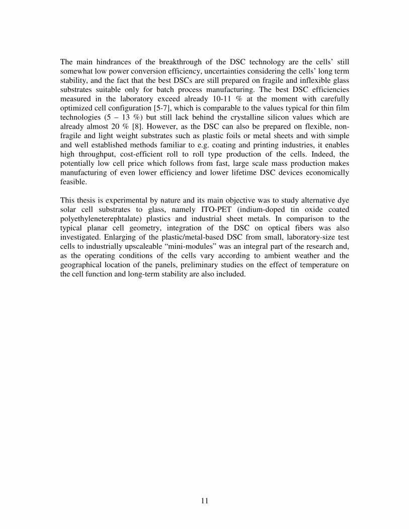
The main hindrances of the breakthrough of the DSC technology are the cells’ still
somewhat low power conversion efficiency, uncertainties considering the cells’ long term
stability, and the fact that the best DSCs are still prepared on fragile and inflexible glass
substrates suitable only for batch process manufacturing. The best DSC efficiencies
measured in the laboratory exceed already 10-11 % at the moment with carefully
optimized cell configuration [5-7], which is comparable to the values typical for thin film
technologies (5 – 13 %) but still lack behind the crystalline silicon values which are
already almost 20 % [8]. However, as the DSC can also be prepared on flexible, non-
fragile and light weight substrates such as plastic foils or metal sheets and with simple
and well established methods familiar to e.g. coating and printing industries, it enables
high throughput, cost-efficient roll to roll type production of the cells. Indeed, the
potentially low cell price which follows from fast, large scale mass production makes
manufacturing of even lower efficiency and lower lifetime DSC devices economically
feasible.
This thesis is experimental by nature and its main objective was to study alternative dye
solar cell substrates to glass, namely ITO-PET (indium-doped tin oxide coated
polyethyleneterephtalate) plastics and industrial sheet metals. In comparison to the
typical planar cell geometry, integration of the DSC on optical fibers was also
investigated. Enlarging of the plastic/metal-based DSC from small, laboratory-size test
cells to industrially upscaleable “mini-modules” was an integral part of the research and,
as the operating conditions of the cells vary according to ambient weather and the
geographical location of the panels, preliminary studies on the effect of temperature on
the cell function and long-term stability are also included.

12
1.3 Thesis outline
The outline of this thesis is as follows:
Chapter 1 presents the background and the main objectives of the study.
Chapter 2 describes the principles behind the operation of PV devices, especially those of
the DSC, and discusses the state-of-the-art in DSC research. DSC materials and
manufacturing methods are introduced and special emphasis is put on alternative
substrates to glass.
Chapter 3 presents the research methods and measurement techniques used in the study.
Chapter 4 describes the experimental part of the study, i.e. cell preparation,
measurements and data analysis.
Chapter 5 gives a summary and overview of the results, reported originally in
Publications I – VIII. The results are discussed and compared to previous scientific
findings in the field.
Chapter 6 consists of more general conclusions and discussion of the topic and Chapter 7
lists the references used in this study.

13
2 Dye-sensitized solar cells (DSC)
2.1 Background, motivation and current status of solar energy utilization
Of all renewable energy sources, solar power is one of the most easily exploitable,
endlessly and constantly abundant, silent, and adaptable to wide variety of applications
from several hundred MW outdoor power plants that produce both heat and electricity [9]
to small off-grid systems that can power areas of rural settlement and dispersed
development. In addition to their basic function which is energy production, the latter
applications can also have big social impact on areas such as Africa, where big parts of
the population still live in primitive conditions and extreme poverty. For example, solar-
powered fridges enable transport and storage of vaccines and drugs in hot climate and
solar cookers can replace open fires that typically consume large amounts of wood which
collection both works in favor of desertification and keeps women tied to household
chores. In houses, solar-powered LED (light-emitting diode) lights can replace inefficient
and toxic kerosene lamps traditionally used for illumination, thus providing properly lit
environment for example for children to study. On even smaller scale and especially with
the new, flexible PV technologies, solar energy can also be used to run low-power
consumer electronics such as laptop computers and mobile phones or it can be integrated
to textiles. These “intelligent”, power-generating garments are an interesting approach
especially from the viewpoint of military and camping equipment manufacturers and can
be utilized in vital function monitoring systems which are used in e.g. hospitals and
geriatric/disabled people care units. Some solar cell types can also be directly integrated
on building materials, thus realizing products such as electricity-generating roofings and
facades, or, due to their transparency, be used as partially shadowing windows that at the
same time produce power to the indoor functions of the house. The constantly expanding
field of printed electronics also benefits from thin, flexible solar cells that can be
manufactured with the same techniques as the main devices.
To private customers, PV’s viability and attractiveness lie in the systems’ low need for
maintenance and silent operation, the constantly increasing lifetime of the PV panels
(current estimate being already 30 years [8]) and at the same time lowering prices, and
the system reliability: the system efficiency stays well within 80 % of the initial value the
whole lifetime of the product, which is why the energy payback time may be as low as
only a few years [8]. As solar energy is produced locally, it also increases energy
independence and creates jobs. Even in countries where sun conditions are not ideal, like
Finland, utilizing solar power works as an energy saving procedure and technological
know-how related to the topic can be an important export product in the future.
The total amount of solar radiation intercepting Earth is approximately 174 PW (Figure
1), which is over 10 000 times the entire global energy consumption [9]. Also, the area
that needs to be covered with solar panels to power the whole Earth is no more than
100 000 km2 – only one third of the land area of Finland. Or, to produce electricity to
whole Europe, only 2 % of the continent’s land area needs to be covered with PV panels

14
[8]. These figures give indication of the enormous potential that lies in the Sun, even if
practical issues such as transporting the power with minimal losses or finding big enough
continuous land areas in climates optimal for solar energy production for large scale
power plants obviously set limitations to its full scale utilization.
Figure 1. Solar energy intercepting Earth [9].
When compared to the traditional, fossil fuel based energy production, solar power is still
somewhat marginal phenomenon, contributing to the global energy usage by only 0.54 %
[9]. Of this, the predominant part is solar heat and only 0.04 % solar electricity, the
cumulative total of installed PV being ca. 9 GW up to this day [8, 9]. However, the
average annual market growth of the photovoltaic industry has been 35 – 40 % for
several years already, and, for example 2007, grid-connected PV was the fastest growing
source of energy with its 83 % increase [9]. The current leaders in photovoltaics are
Spain and Germany which, according to 2008 statistics, contributed to the 6 GW total of
PV installed globally that year with 2.46 GW and 1.86 GW, respectively (Figure 2) [10].
The market growth was impressive especially in Spain: 285 % from the previous year
[10]. These numbers, along with the constantly increasing production capacity of solar
panels (doubling every two years [9]), lowering costs and technological advancements in
panel efficiency and long-term stability, show that despite its reputation of being a niche
energy source, solar power is an attractive and profitable investment which has even been
proposed as the most likely replacement for fossil fuels in the future. Oil, gas, and coal
might never be completely exhausted, but their utilization becomes more and more

15
difficult and expensive in the near future, which has made even the big oil companies
such as Shell and BP to invest large sums in solar energy research [11, 12].
Figure 2. Distribution of PV installed globally in 2008 [10].
Even if the PV technologies are well established and the modern solar power systems are
relatively easy to install it still needs political will to make solar energy profitable to a
common customer. The success of especially Germany in solar energy utilization lies in
its feed-in tariff system, in which the consumers are able to sell the electricity produced
by their PV panels back to the electricity company, and with higher price than the price
of the regular grid electricity, which shortens the PV system payback time considerably.
Similar systems exist also in Spain, Italy, France and Greece [8].
Despite the constantly lowering manufacturing costs of the PV panels, the main problem
in the breakthrough of solar power is its still high price compared to grid electricity – for
example, EPIA (European Photovoltaic Industry Association) predicts that it will take at
least ten years still until PV will become truly economically competitive with
conventional grid power in Europe [8]. One of the reasons for this is the difficult and
energy intensive manufacturing process of silicon solar panels which still contribute to all
installed PV with 90 % [8]. Shortage of ultra-pure solar grade silicon may also loom in
the future, as also the microchip and sensor industries consume large amounts of this raw
material. Traditional silicon PV panels are also heavy, inflexible, suitable for only limited
number of applications and usually protected by glass sheets which may break easily.
New technologies are thus called for to realize more economically feasible, large scale
utilization of solar energy.
16
2.2 Principles of photovoltaic conversion
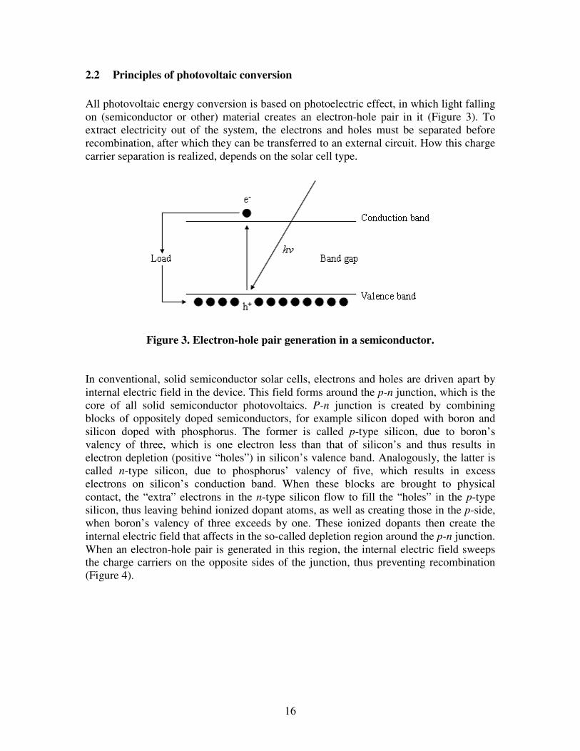
All photovoltaic energy conversion is based on photoelectric effect, in which light falling
on (semiconductor or other) material creates an electron-hole pair in it (Figure 3). To
extract electricity out of the system, the electrons and holes must be separated before
recombination, after which they can be transferred to an external circuit. How this charge
carrier separation is realized, depends on the solar cell type.
Figure 3. Electron-hole pair generation in a semiconductor.
In conventional, solid semiconductor solar cells, electrons and holes are driven apart by
internal electric field in the device. This field forms around the p-n junction, which is the
core of all solid semiconductor photovoltaics. P-n junction is created by combining
blocks of oppositely doped semiconductors, for example silicon doped with boron and
silicon doped with phosphorus. The former is called p-type silicon, due to boron’s
valency of three, which is one electron less than that of silicon’s and thus results in
electron depletion (positive “holes”) in silicon’s valence band. Analogously, the latter is
called n-type silicon, due to phosphorus’ valency of five, which results in excess
electrons on silicon’s conduction band. When these blocks are brought to physical
contact, the “extra” electrons in the n-type silicon flow to fill the “holes” in the p-type
silicon, thus leaving behind ionized dopant atoms, as well as creating those in the p-side,
when boron’s valency of three exceeds by one. These ionized dopants then create the
internal electric field that affects in the so-called depletion region around the p-n junction.
When an electron-hole pair is generated in this region, the internal electric field sweeps
the charge carriers on the opposite sides of the junction, thus preventing recombination
(Figure 4).

17
Figure 4. A p-n junction in dark (left) and in light (right). Eint = internal electric
field. The black circles symbolize net negative charge, the white circles net positive
charge.
Energetically, the same can be understood by “bending” of the valence and conduction
bands. In an undoped semiconductor, the Fermi level is located in the middle of the band
gap. When the semiconductor is doped with atoms with “extra” electrons, the Fermi level
shifts upwards and analogously, when the dopant causes electron depletion, the Fermi
level moves lower. When the oppositely doped blocks are brought to contact, the flow of
electrons from the n-side to the p-side shifts the n-side conduction band lower and
correspondingly, the flow of holes from the p-side to the n-side moves the p-side valence
band higher on electronic energy scale. As a result of this, the Fermi levels match
throughout the junction. Because of this band “bending”, it is energetically favorable for
the photogenerated charge carriers to move across the junction, i.e. electrons created on
the p-side flow “downwards” to the n-side and holes created in the n-side move
“upwards” to the p-side. Typically, either n- or p-side is doped heavier so the depletion
region reaches further in this side and the most of the charge carriers can be collected
there. This offers also the benefit that the junction itself can be brought close to the solar
cell surface, thus maximizing the amount of absorbed photons.
In DSC, the charge carrier separation happens on an interface between electronic and
ionic conductors (Figure 5). The semiconductor typically used in these cells, titanium
dioxide, has band gap too wide for visible light to evoke photoelectric effect, but the
electrons are fed into the material from electronically excited dye molecules adsorbed on
its surface. In this process, the dye gets oxidized, i.e. a positive charge is created. For the
electron injection process to continue the dye needs to be reduced back to its ground
state, which is done by electrolyte which contains a redox couple and is in contact with
the TiO2 layer. Thus, the positive “hole” is transferred into the electrolyte as the oxidized
form of the redox couple and the electrons are fed into the TiO2. Because the holes can

18
not move in the TiO2 and electrons in the electrolyte, charge carrier separation is
achieved. The electron injection from the dye to the TiO2 is energetically favorable
because the excited electronic state of the dye is located slightly higher than the TiO2
conduction band. The injection process is also several decades faster than the competing
reactions, i.e. relaxation of the dye back to the ground state or recombination (the details
of the charge transfer processes in the DSC are discussed in more detail in Chapter 2.3).
Figure 5. Charge carrier separation in the DSC.
2.3 DSC structure and operating principle
The DSC differs from other solar cells types both by its basic construction and the
physical processes behind its operation. Unlike the 1st and 2
nd generation PV devices
based on solid semiconductor materials, the typical DSC configuration combines solid
and liquid phases. Electricity is generated on the photoelectrode, which is a nanoporous
TiO2 film sensitized with a monolayer of visible light absorbing dye and penetrated with
a redox electrolyte. The TiO2-electrolyte network is sandwiched between two conductive
substrates that also work as current collectors. The opposite substrate to the TiO2 layer,
the counter electrode, is coated with a material capable of catalyzing the redox reaction in
the electrolyte. Thus, the DSC resembles more an electrochemical cell than a
conventional p-n junction solar cell.
Research on wide band gap oxide semiconductors sensitized with dyes began already in
the late 1800’s, related to photography. The first studies on dye-sensitized TiO2 and ZnO
photoelectrodes were done in 1960’s and 1970’s, but due to a limited amount of dye that
could be adsorbed on macrocrystalline semiconductors and too narrow spectral
absorbance range of the dyes the photocurrent and cell efficiency stayed on very modest
level [3]. Improvement to this was achieved in the early 1990’s, thanks to
nanotechnology and development of better dyes. Nanocrystalline TiO2 enabled drastic
multiplying of the effective surface area of the photoelectrode for the dye to adsorb, and

19
the new ruthenium bipyridyl organometallic complexes (Figure 6) had absorbance range
from visible to near-infrared wavelengths [3].
Figure 6. Molecular structures of some common dyes, the so-called N-719 and
“black dye” (BD) [3].
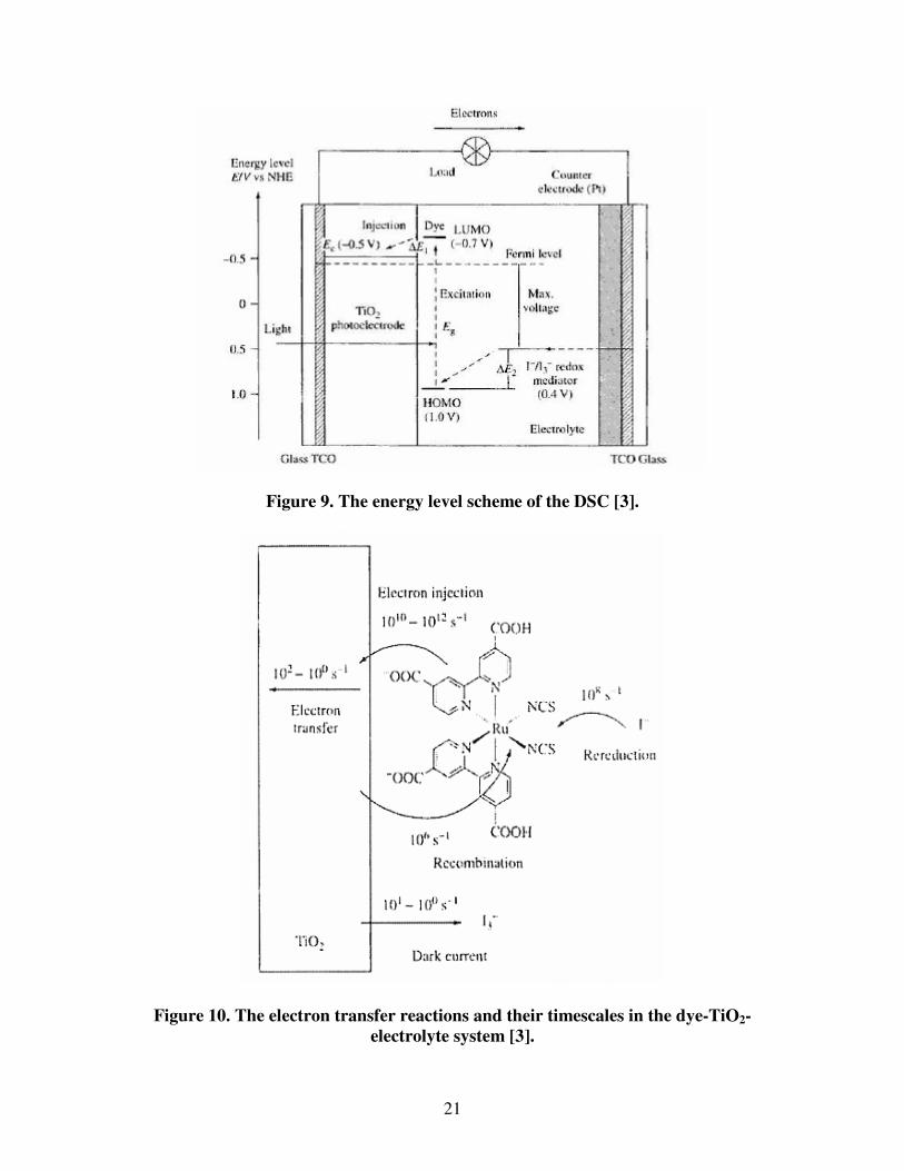
The basic DSC structure and operating principle are presented in Figure 7. Photon
absorption induces a metal-to-ligand type electronic transition between the HOMO
(highest occupied molecular orbital) and LUMO (lowest unoccupied molecular orbital) of
the dye. Since the LUMO is located in the vicinity of the ligands (pyridyl π-orbitals) the
electron injection to the TiO2 is spatially favorable. Efficient electron injection is further
enhanced by the strong electronic interaction that forms when the dye bonds to the TiO2
with the ligand carboxyl groups (Figure 8) and the energetic location of the TiO2
conduction band in relation to the LUMO of the dye (Figure 9). Efficient charge
separation is, on the other hand, achieved because the electrons and holes travel in
different mediums – this prevents bulk recombination which is a problem in conventional
p-n junction cells. The competing reactions, i.e. recombination of the photogenerated
electrons with the oxidized form of the dye or the redox species in the electrolyte (Figure
10; the latter reaction referred to as “dark current” in the picture) proceed also several
decades slower than the electron injection process. In addition to that, the electrolyte
cations and protons released in the dye adsorption process intercalate to the TiO2 surface
and lattice where they, together with the negative species in the electrolyte, form a
Helmholtz dipole layer on the photoelectrode surface. This enhances charge separation
even further.
The amount of current that the cell is able to generate is determined by the energetic
distance of the HOMO and LUMO of the dye, which equals the band gap in inorganic
semiconductors. The maximum voltage, on the other hand, is defined as the difference
between the redox level of the electrolyte and the Fermi level of the TiO2 (Figure 9).
With iodide/triiodide redox couple, this difference is ca. 0.9 V, though slight variation is
caused by the electrolyte composition due to species adsorbed on the TiO2 surface, which

20
may alter the Fermi level position somewhat. Also, there is always some recombination
in the cell which lessens the amount of electrons in the TiO2 film, thus lowering the
Fermi level and decreasing the cell voltage.
Figure 7. The structure and operating principle of the DSC. Modified from the
picture presented in [13].
Figure 8. Dye bonding to the TiO2. Two possible bonding mechanisms (ester
bonding and carboxylate bidentate coordination) presented. Modified from a
picture from [3].
21
Figure 9. The energy level scheme of the DSC [3].
Figure 10. The electron transfer reactions and their timescales in the dye-TiO2-
electrolyte system [3].

22
After injection, electrons diffuse in the nanocrystalline TiO2 network to the conductive
coating of the substrate, from which they can be transferred to an external circuit. There
exist various models for the electron diffusion in the TiO2 film but thermally activated
trapping/detrapping mechanism along localized energy levels below the TiO2 conduction
band edge seems the most realistic one, in the light of experimental evidence [14-17].
The electron injection to the TiO2 leaves the dye molecule on an oxidized state so, in
order for the current generation to continue, the dye must be reduced back to its ground
state. This is done by the redox couple in the electrolyte. The most commonly used redox
couple, and the one that gives the best cell efficiencies when combined with TiO2, is
iodide/triiodide. The oxidized dye gets electrons from the iodide ions which, in turn, get
oxidized to triiodide in the process. The triiodide ions then diffuse to the counter
electrode, where they get reduced back to iodide by the electrons returning from the
external load. Thus, the cell operation is based on consecutive reduction/oxidation cycles
and, in an ideal cell, no chemical substances are permanently transmuted. The most often
used counter electrode catalyst for the triiodide/iodide reduction reaction is platinum,
though also carbon materials and certain conductive polymers have been successfully
employed in this function [18].
The chemical reactions going on in the cell can be summarized as follows:
At the photoelectrode (S0 = the ground state of the dye; S
* = the excited state of the dye;
S+ = the oxidized state of the dye):
• Light absorption: ∗→+ ShS 222 0 ν (1)
• Electron injection: )(222 2TiOeSS −+∗ +→ (2)
• Dye reduction and iodide oxidation: −−+ +→+ 3
0232 ISIS (3)
• Overall: )(223 23 TiOeIhI−−− +→+ ν (4)
At the counter electrode:
• Triiodide reduction: −−− →+ IeI 323 (5)
23
2.4 DSC basic materials and manufacturing methods
2.4.1 Substrates
Requirements for a good DSC substrate are low sheet resistance which should also be
independent of temperature up to 450 – 500 oC (in case when the electrode post-treatment
requires sintering), high transparency, and ability to prevent impurities such as water and
oxygen from entering into the cell. The traditional approach is to build the DSC on
transparent conducting oxide (TCO) coated glass sheets. The most often used TCOs are
fluorine- and indium-doped tin oxides, whose sheet resistances are around 10 Ω/. Whilst
glass is obviously an effective barrier towards water and oxygen penetration into the cell,
its disadvantages are fragility, rigidity, heavy weight and high price. ITO’s sheet
resistance also increases with temperature so ITO-coated glass is not the best option for
cells where high temperature treatments are needed.
Alternative substrate materials such as plastic foils and metal sheets overcome most of
the glass’ problems. Conductive plastics, like ITO-PET and ITO-PEN (indium-doped tin
oxide coated polyethylenenaphtalate), are light weight and flexible, whereas metals are
also mechanically robust, cheap, and their electrical conductivity is superior compared to
all other substrate materials. The last factor plays a crucial role in cell size upscaling,
since the main part of the total ohmic losses in the cell are due to lateral resistance on the
substrate surface. It has also been noticed that substrate-mediated recombination is lower
from stainless steel than from glass [19]. Disadvantages of plastics include low
temperature tolerance, max. 150 – 160 oC, for ITO-PET high sheet resistance, around 60
Ω/, and uncertainties considering the oxygen and water penetration. For metals, the
main problem is the traditionally used, iodine-containing electrolyte. Triiodide ions are
corrosive, and thus far only stainless steel and titanium have shown enough chemical
stability in the iodine electrolyte to be successfully employed as DSC substrates [19-27].
Long-term stability of metal-based cells is still unknown, though, and requires further
studies before this DSC type can be transferred to large scale manufacturing. However,
the main spur behind the alternative substrate research is the flexibility of both the plastic
and metal substrates which enables roll-to-roll type manufacturing of the DSC,
potentially leading to high volume production of low cost solar cells with wide variety of
applications.
2.4.2 Photoelectrode
The semiconductor material that forms the core of the photoelectrode (PE) should be
chemically stable and inert towards the electrolyte species, it should have a lattice
structure suitable for dye bonding, its conduction band should be located slightly below
the LUMO level of the dye in order to facilitate efficient electron injection, and it should
be available in nanostructured form to enable high enough dye loading. Titanium dioxide
fulfills these requirements – in addition to that, it is also cheap and easily available
24
because of mass production. The material is in wide use for example in pigments and
paints and, due to its non-toxicity, even in cosmetic, hygiene and food products. Another
semiconductor oxide that has been employed in the DSC is zinc oxide but there have
been problems for example with the dye desorption [28] which is why TiO2 is still the
most widely used DSC photoelectrode material.
TiO2 exists in three crystalline forms, anatase, rutile, and brookite, of which the anatase
structure is the most suitable for DSC applications. The typical TiO2 nanoparticle size in
the PE film is 10 – 30 nm, though larger particles up to 300 – 400 nm are sometimes
added to the film to increase the path length of the absorbed photons by scattering
(improved light harvesting efficiency). The optimal PE film thickness is 10 – 15 µm – if
the film is very thin the dye loading remains too low whereas with too thick films, the
distance the excited electrons generated on the electrolyte side of the PE film have to
travel before reaching the current collector becomes so long that increased recombination
probability starts to decrease the cell efficiency.
Screen-printing is a typical TiO2 layer deposition method, with which large quantities of
even quality films can be prepared with high speed (on laboratory scale, technique called
“doctor-blading”, in which the TiO2 precursor is applied through a hand-cut tape mask is
often employed). Several research groups prepare their own TiO2 precursor materials but
there exists also commercial titania pastes specifically designed for screen-printing
technique – in addition to the TiO2 nanoparticles they contain some high viscosity
organic solvent, binders, pH-adjusting agents, and morphology controlling agents. After
the film deposition the solvent and other organic ingredients have to be removed, which
is done by sintering the film in 450 – 500 oC for half an hour minimum. In this treatment
the individual TiO2 nanoparticles also “neck” together and adhere more tightly to the
substrate surface which decreases the interparticle resistance, thus facilitating efficient
electron diffusion in the film, and the resistance for the electron transfer from the TiO2
network to the substrate. Unfortunately, this sintering treatment, which drastically
improves the TiO2 film quality and also its mechanical stability can not be employed with
plastic substrates, due to their low temperature tolerance. One promising technique for
low temperature PE film preparation is spraying suspension of TiO2 nanoparticles in high
volatility solvent (e.g. ethanol) on heated substrate and then mechanically compressing
the resulting powder layer. Titania pastes suitable for low temperature sintering have also
been developed but the problem of inadequate interparticle necking and thus lower cell
efficiency, due to slower electron transport in the film and thus higher recombination
probability, still remains with these materials too.
Dye sensitization of the PE is done simply by soaking the TiO2 film in the dye solution
(anhydrous ethanol being the common solvent, though various nitriles have also been
used), the soaking time typically being overnight minimum, though the process can be
sped up by heating the solution. The dye is one of the most expensive components of the
cell, due to the complex structure and demanding, multistep synthesis of the molecule,
but since its amount in the solution is very small, typically of the order 10-4
M, its effect
on the overall manufacturing costs of the cell remains reasonably low. In addition to the
ruthenium organometallic complexes mentioned already in chapter 2.3, other dyes such

25
as coumarins, eosins, perylenes and even natural dyes extracted from berries have been
employed in the DSC, though the highest efficiencies have still been obtained with the
Ru-complexes. As a matter of fact, the molecular structure of the dyes and the electron
transfer processes in the dye excitation resemble those of the chlorophyll molecule in
green plants, which is why the DSC operating principle has sometimes been called
“artificial photosynthesis”.
2.4.3 Electrolyte
In addition to the redox couple – like the most commonly used iodide/triiodide – the
electrolyte usually contains some “blocking agent” that adsorbs on the PE on those
surface sites not occupied by the dye to prevent recombination, i.e. electron leakage from
the TiO2 back to the electrolyte. 4-tert-butylpyridine, guanidinium thiocyanate and 4-
guanidinobutyric acid are some molecules used in this purpose [2, 29]. Due to suppressed
recombination, the cell open circuit voltage increases. The requirements for the
electrolyte solvent are its ability to dissolve the other ingredients and preferably low
volatility combined with high viscosity to facilitate fast ionic diffusion between the
electrodes. Typical solvents used in the DSC electrolyte are various nitriles (aceto-,
methoxypropio-, valero-, butyro-), carbonates (ethyl-, propyl-) and their mixtures. Liquid
electrolyte can also be gelatinized, for example with certain polymers (e.g.
polyvinylidenefluoride-hexafluoropropylene, PVDF-HFP) or silica nanoparticles [30].
While this does not remove the problem of the cell “drying” in case of structural damage
to the substrates, it does prevent electrolyte leakage. Obviously, the liquid electrolyte is
the weak link considering the cells’ long-term stability which is why solid hole
conductors such as copper iodide (CuI), copper thiocyanate (CuSCN), copper bromide
(CuBr) complexes, 2,2′7,7′-tetrakis-(N,N-di-p-methoxyphenyl-amine)-9,9′-spirobifluo-
rene (spiro-MeOTAD), and the conducting polymer poly(3,4-ethylenedioxythiophene)
(PEDOT) have also been studied as its replacement [31-41]. Either the cell efficiency or
its stability have not been satisfactory with these – one reason being the solid material’s
poor penetration into the pores of the TiO2 layer – which is why iodine-based liquid
electrolyte is still the most often used alternative in the DSC. An example of a typical
electrolyte composition is 0.5 M lithium iodide (LiI), 0.05 M iodine (I2), and 0.5 M 4-
tert-butylpyridine in 3-methoxypropionitrile (triiodide ions are generated in a reaction of
molecular iodine with the iodide ions). The amount of iodine may vary according to the
electrolyte layer thickness – in cases where the light enters the cell from the counter
electrode (CE) side, through the CE and electrolyte (e.g. if the PE is deposited on opaque
metal sheet), the shadowing effect of the dark red triiodide ions in the electrolyte reduces
the amount of photons reaching the PE (iodide ions, on the other hand, are transparent).
When the order of the maximum current the cell should be able to generate is known, the
triiodide concentration and electrolyte layer thickness can be minimized using the
definition for the diffusion-limited current density [42]
l
cnFDi II −−= 33
lim
2, (6)
26
where n is the number of electrons transferred in the redox reaction, F the Faraday
constant, DI3- the triiodide diffusion coefficient, cI3- the triiodide concentration, and l the
distance between the electrodes.
There is also an interesting, new group of DSC electrolytes in which so-called ionic
liquids, or room temperature molten salts are utilized [43-45]. Ionic liquids are fluids
with no vapor pressure at all which eliminates the problem of electrolyte drying in case of
fractures on the substrate. Typically, ionic liquids are salts of iodine with a large, often
imidazole-based cation, for example 1-methyl-3-propylimidazolium iodide (PMII) or 1,2-
dimethylimidazolium iodide (DMPII). Thus, ionic liquid works as a source of iodide ions
and also as a solvent, due to its fluidic nature. The problem of these electrolytes is,
however, the high viscosity of many ionic liquids, which slows down the ionic diffusion
and tends to keep cell efficiencies down. Some ionic liquids are also hygroscopic which
means that special conditions, e.g. dry air or nitrogen atmosphere is needed for cell
preparation and storage of materials.
2.4.4 Counter electrode
For DSCs deposited on glass, thermally deposited or sputtered platinum is the most
widely used CE catalyst. The advantages of Pt are its high catalytic activity towards the
iodide/triiodide redox reaction which is why only a few nanometer layer of Pt is required
– this keeps the cell manufacturing costs low even if Pt is an expensive element, and
because the thin Pt layer is almost transparent, platinized counter electrodes can be
employed also in cells which require reverse lighting (i.e. lighting from the CE side).
Platinum is also chemically stable in the electrolyte, i.e. no remarkable dissolution over
time from the CE have been noticed (in case the CE catalyst dissolves and diffuses to the
PE, it may act there as recombination centers, thus decreasing the cell efficiency). In the
thermal method, an alcoholic solution of platinum salt (e.g. PtCl4 or H2PtCl6) is spread on
the substrate and after the solvent evaporation, the substrate is fired in an oven in 385 oC
for ca. 15 minutes. This results in reduction of metallic platinum as tightly adhered
nanoscale clusters on the substrate surface [46]. Due to high temperature involved, this
method is naturally not suitable for plastic substrates but sputtering, which is a well
known and widely applied method for thin film coatings, can be employed for low
temperature tolerance substrates as well.
Since platinum is an expensive catalyst, even if the consumption is relatively low, other
materials such as nanostructured and/or activated carbon and conducting polymers such
as PEDOT or PANI (polyaniline) have been studied as its replacement [18]. The main
problem with these materials is that often rather thick layers of them are needed in order
to reach high enough catalytic activity. This slows down the cell manufacturing process
and, as thick catalyst layers also absorb light, these kind of CEs are not suitable for
reverse lighting cells. Carbon materials are also typically deposited from sprayable
suspensions (cf. the TiO2 suspension spraying technique for plastic substrates), and the
mechanical integrity of the resulting powder film is achieved with simple compressing.
Since in the compressing process no chemical or physical bonds between the powder
27
particles and the substrate are formed the stability this kind of a film has against
mechanical stress is not as good as that of a few nanometer layer of thermally deposited
or sputtered platinum.
2.4.5 Cell assembly
The electrodes are typically laminated together on a hot plate, using a thermoplastic
ionomer resin film (e.g. Surlyn®, Bynel
®) as a sealant and spacer to prevent the cell from
short circuiting. So-called glass frit technique can also be used but since it requires high
temperatures, it is suitable only for glass substrate cells [47]. After this, the electrolyte is
inserted into the cell through special filling channels drilled on either one of the
substrates or cut to the spacer film on the sides of the cell. The filling channels are sealed
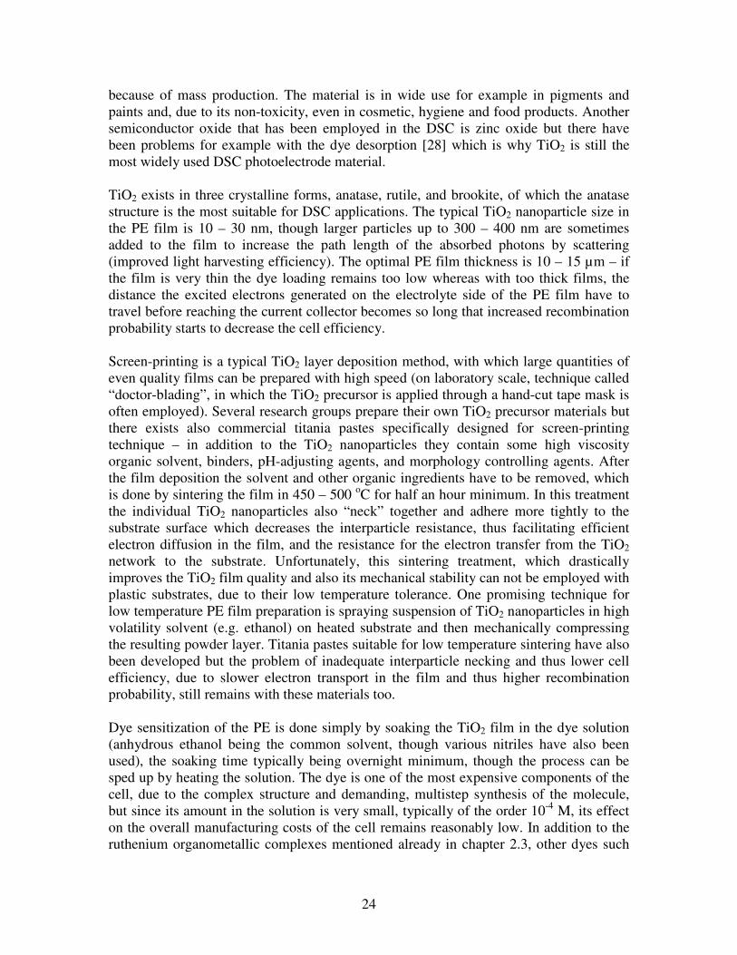
and the external current collectors applied, after which the cells are ready for
encapsulation. Figure 11 presents an example of a manufacturing process of a flexible
and low temperature spray-deposited DSC.
Figure 11. A low-temperature preparation process for flexible DSCs.
2.5 State of the art in DSC on different substrates
The highest reported DSC efficiencies at the moment are around 10-13 % with all-glass
substrates, which is well comparable for example to amorphous silicon solar cells [48].
The highest flexible DSC efficiency is close to that also: 8.6 % with a stainless steel PE
cell [27] (Pt-sputtered ITO-PEN as the CE). With stainless steel CE, even 9.15 % was
achieved, using high active surface area carbon black as a catalyst, though in this case the
PE was deposited on glass, so the cell was not completely flexible [18]. Titanium has also
been successfully used as the PE substrate, giving efficiency of 7.2 % (flexible cell with
platinized ITO-PEN as the CE) [24]. With all-plastic substrates, a promising 7.4 % has
been achieved utilizing, in the deposition of the TiO2 film, the suspension spraying and
compressing technique mentioned earlier [49]. In [49], also the TiO2 nanoparticles were
self-synthesized and very high compressing force was noticed to be the key factor in
improving the compressed PE cell efficiency. Typically, the plastic PE cell efficiencies
have been on the range 5-6 %, using methods such as hydrothermal crystallization [50-
52], chemical vapor deposition of Ti alkoxides [53-55] combined with microwave or UV
treatment [53-56] or laser sintering [57] as a replacement of the high temperature post-
treatment of the TiO2 film.

28
It must be noted here, however, that cell efficiencies are not automatically comparable –
for example, different electrolyte solvent, different manufacturer of the TiO2
paste/particles or different substrate pre-treatment methods may directly affect the
efficiency. In top efficiency cells, also several “efficiency-boosting” means such as anti-
reflectance coatings, large, scattering TiO2 particles in the PE film and additional
recombination blocking layers between the substrate and the TiO2 film may have been
utilized. In addition to this, the top efficiencies are typically obtained with very small
cells (active area < 1 cm2). When the active area size increases the substrate sheet
resistance is bound to cause remarkable ohmic losses unless metal substrates or additional
current collector structures embedded to the substrate material are used. When the cells
are further combined to modules, additional resistance occurs also in the wirings between
the individual cells.
All in all, high efficiencies alone are not enough to make the DSC appealing to
consumers and investors – long-term stability is still a relatively little studied issue,
especially in the case of metal- and plastic-based cells. Stability improvement has been
achieved with development of new dyes, for example with hydrophobic Z-907 less than
10 % drop in efficiency in 1000 hours 80 oC heating test was measured [58]. Also, in
simple light-soaking tests even longer stability times have been reported, like 12 000
hours at one Sun [59] and 8000 hours at 2.5 Sun [60]. However, factors like the chemical
stability of the electrolyte, the chemical stability of the metal substrates, the penetration
of water and oxygen into the cell (especially with plastic substrates) and the effect of
varying environmental conditions during the cell operation are still topics that need more
thorough research to make this technology fully competitive against the traditional
crystalline silicon PV devices. The special treatments that may be needed to increase the
DSC efficiency to maximum also cause additional, possibly expensive steps to the
manufacturing process and thus may increase the cell price too much.
Commercialization-wise, DSC-based PV devices are not yet generally available in the
same way silicon and some types of thin film panels are. There exist several companies
though which are already very close: For example, Australian Dyesol, Inc. is the current
leader in industrial-scale DSC material development and marketing [61]. Their large
scale cooperation with the leading steel industries also indicates that metal-based DSC
looks like a promising route to bring this technology out of laboratory and into public
use. Other companies that already have automated, high throughput DSC production are
G24 Innovations, Inc. in Great Britain [62] and Konarka, Inc. in the USA [63]. Common
to all these companies is roll-to-roll manufacturing of the DSC on flexible, plastic or
metal substrates, products including for example mobile phone chargers and “electric
fabric” (Figure 12). Dyesol also manufactures more conventional, glass-based BIPV
(building integrated photovoltaics) tiles and panels (Figure 13).

29
Figure 12. Examples of flexible DSC products. Pictures © G24 Innovations.
Figure 13. BIPV DSC panels and tiles. Pictures © Dyesol.

30
3 Research methods
Information about a solar cell performance can be obtained with several experimental
methods, including spectroscopical techniques and electron microscopy for materials
characterization. However, since the central results included in this thesis were from
current-voltage curve and electrochemical impedance spectroscopy measurements, only
these two methods are described here more detailedly.
3.1 Current-voltage curve measurements
Current-voltage curve measurements are the most central way to characterize the PV
device performance. In these measurements, the lighted cell is put under a reverse bias
voltage scan and the generated photocurrent recorded (Figure 14). At the point where the
external bias voltage is zero, there is no opposing force to the current flow from the cell
and the maximum current the cell is able to generate, the short circuit current Isc, can be
measured. Accordingly, at the point where the external voltage equals the maximum
voltage of the cell, the open circuit voltage Voc, no current flows. In practice, and to make
the results independent of the cell size, current density, expressed in A/cm2, is used
instead of plain current.
Figure 14. An example of an IV-curve and a power curve of a DSC.
31
From the power curve the maximum power point can be detected and from the current
and voltage at this point, Impp and Vmpp, along with Isc and Voc, the fill factor (FF) of the
cell can be calculated from the equation
scoc
mppmpp
IV
IVFF
⋅
⋅= . (7)
Fill factor measures the “squareness” of the curve. For example, resistive losses in the
cell show directly from the shape of the IV-curve, making it “flatter” and decreasing the
fill factor. The cell efficiency (η) can be calculated using the fill factor, or directly from
the Impp and Vmpp using the equation
AP
IV
AP
FFIV
in
mppmpp
in
scoc
⋅
⋅=
⋅
⋅⋅=η , (8)
where Pin is the power of incident light on the cell and A is the photoactive area of the
cell, i.e. in the case of the DSC, the area of the dye-sensitized TiO2 film.
In practice, the cells are measured under artificial lighting in a solar simulator. To ensure
that the measurement results are comparable even if the used lighting is different, so-
called standard measurement conditions are defined. They are: 25 oC temperature, 1000
W/m2 power of incident light, and AM 1.5 G solar spectrum. Temperature and power of
incident light can be adjusted with technical means, but to adjust the measured
photocurrent to correspond to that obtained with the AM 1.5 G standard spectrum, so-
called spectral mismatch factor M for the used simulator has to be determined [64]. It can
be calculated using a standardized reference cell (for example a monocrystalline silicon
cell characterized in an officially, internationally recognized standardizing laboratory)
with the formula
simref
stdref
stdtest
simtest
I
I
I
IM
,
,
,
,⋅= , (9)
where Itest,std is the current of the measured cell under the standard spectrum, Iref,std the
current of the reference cell under the standard spectrum, i.e. the value which is known
from the standardizing laboratory, Iref,sim the current of the reference cell in the simulator,
and Itest,sim the current of the measured cell in the simulator, after which the corrected
photocurrent for the measured cell is obtained as
M
II
simtest
stdtest
,
, = . (10)
The mismatch factor is obviously valid for only one type of lamps that are used in certain
solar simulator and in certain measurement geometry.
32
3.2 Electrochemical impedance spectroscopy
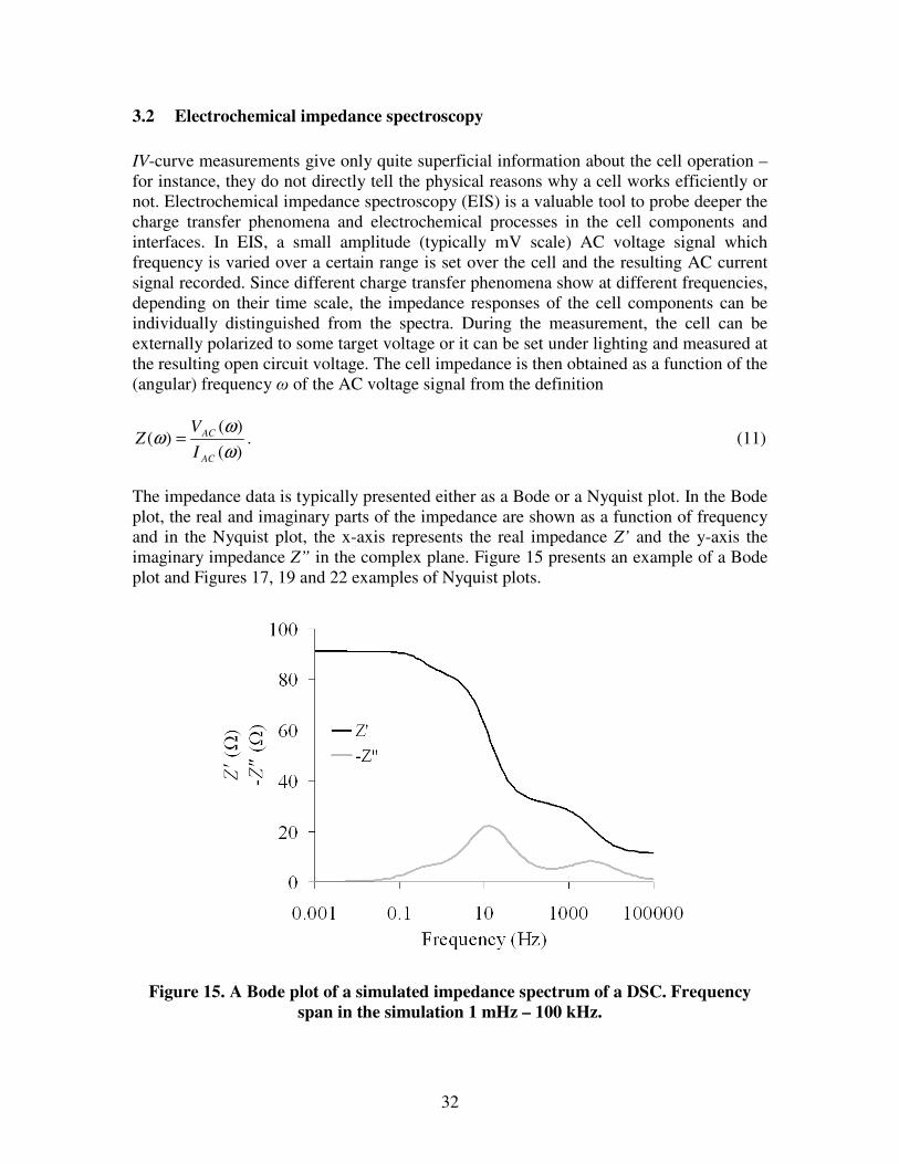
IV-curve measurements give only quite superficial information about the cell operation –
for instance, they do not directly tell the physical reasons why a cell works efficiently or
not. Electrochemical impedance spectroscopy (EIS) is a valuable tool to probe deeper the
charge transfer phenomena and electrochemical processes in the cell components and
interfaces. In EIS, a small amplitude (typically mV scale) AC voltage signal which
frequency is varied over a certain range is set over the cell and the resulting AC current
signal recorded. Since different charge transfer phenomena show at different frequencies,
depending on their time scale, the impedance responses of the cell components can be
individually distinguished from the spectra. During the measurement, the cell can be
externally polarized to some target voltage or it can be set under lighting and measured at
the resulting open circuit voltage. The cell impedance is then obtained as a function of the
(angular) frequency ω of the AC voltage signal from the definition
)(
)()(
ω
ωω
AC
AC
I
VZ = . (11)
The impedance data is typically presented either as a Bode or a Nyquist plot. In the Bode
plot, the real and imaginary parts of the impedance are shown as a function of frequency
and in the Nyquist plot, the x-axis represents the real impedance Z’ and the y-axis the
imaginary impedance Z” in the complex plane. Figure 15 presents an example of a Bode
plot and Figures 17, 19 and 22 examples of Nyquist plots.
Figure 15. A Bode plot of a simulated impedance spectrum of a DSC. Frequency
span in the simulation 1 mHz – 100 kHz.

33
Interpretation of the impedance spectra is done by utilizing so-called equivalent circuits.
In them, the cell components and interfaces are presented as electrical components such
as resistors and capacitors. By fitting the measured impedance spectrum to the equivalent
circuit, numerical values for the parameters such as resistances in the cell components,
capacitances on the electrode surfaces, and diffusion impedance in the electrolyte can be
obtained.
The type of an equivalent circuit used depends on the cell type. The most simple,
symmetrical counter electrode – counter electrode cell can be modeled as an RC-circuit in
series with a resistor, as presented in Figure 16. Also, the Warburg element Ws describing
the impedance for the ionic (Nernstian) diffusion in the electrolyte, Zd, is added. Figure
17 presents a Nyquist plot of a simulated spectrum based on the equivalent circuit in
Figure 16.
Figure 16. A symmetrical CE – CE cell equivalent circuit.
Figure 17. A Nyquist plot for a simulated impedance spectrum for a symmetrical
CE – CE cell. Frequency span in the simulations 1 mHz – 100 kHz.
In Figure 16, the single resistor describes the total ohmic losses in the cell, the cell series
resistance Rs, whereas the RC-circuit the interface between the electrode surface and
electrolyte. Charge transfer resistance Rce measures the activity of the CE catalyst: The
smaller the Rce, more effectively the triiodide reduction reaction proceeds. Electrode
capacitance, on the other hand, originates from the charge accumulation: Accumulation
and orientation of oppositely charged ions from the electrolyte results in formation of a
Helmholtz dipole layer on the electrode surface which works as a miniature capacitor. In
practice, pure capacitance is a valid model only for completely “smooth”, homogenous

34
electrode surface. This is why, in the case of the DSC where surface inhomogenities arise
simply from the fact that the catalyte is not evenly spread or the surface is porous, so-
called constant phase element CPE is used in the equivalent circuits instead of a plain
capacitance. The capacitance of a CPE is defined with the equation
( ) βω
−⋅= i
BZCPE
0
1, (12)
where the pre-factor B0 has units of capacitance and the exponent β is related to the
“flatness” of the semicircle [65]. The more the exponent deviates from one, the farther
the electrode surface is from an ideal capacitor which shows as “flattening” of the
semicircle.
In Figure 17, the larger semicircle on the left, high frequency end of the plot arises from
the Rce – CPEce parallel combination whereas the series resistance can be obtained as the
distance between origin and the start of the Rce – CPEce semicircle. The diffusion
impedance shows as the smaller semicircle on the right, low frequency end of the plot.
Figure 18 presents a “simplified” equivalent circuit for a complete DSC and Figure 19
again a simulated spectrum according to Figure 18. Here, two RC-circuits are used,
another for the photo- and another for the counter electrode. This kind of a simplified
circuit can be used in cases where, in the photoelectrode impedance response, only the
recombination resistance part is shown in the spectrum. In reality, the PE total resistance
Rpe is a combination of the electron transport resistance in the TiO2 film, Rtr, and the
charge transfer resistance for the electron recombination reaction across the TiO2 –
electrolyte interface, Rrec, but the former component typically shows only when the
electron transport in the TiO2 film is somehow “hindered”, i.e. on small external
polarization voltages when the film conductivity is low due to small amount of electrons
in it or in cases where the resistance for the electron transport is high because of poor
film quality. So, in the equivalent circuit in Figure 18, Rpe equals Rrec.
Figure 18. A simplified complete DSC equivalent circuit.
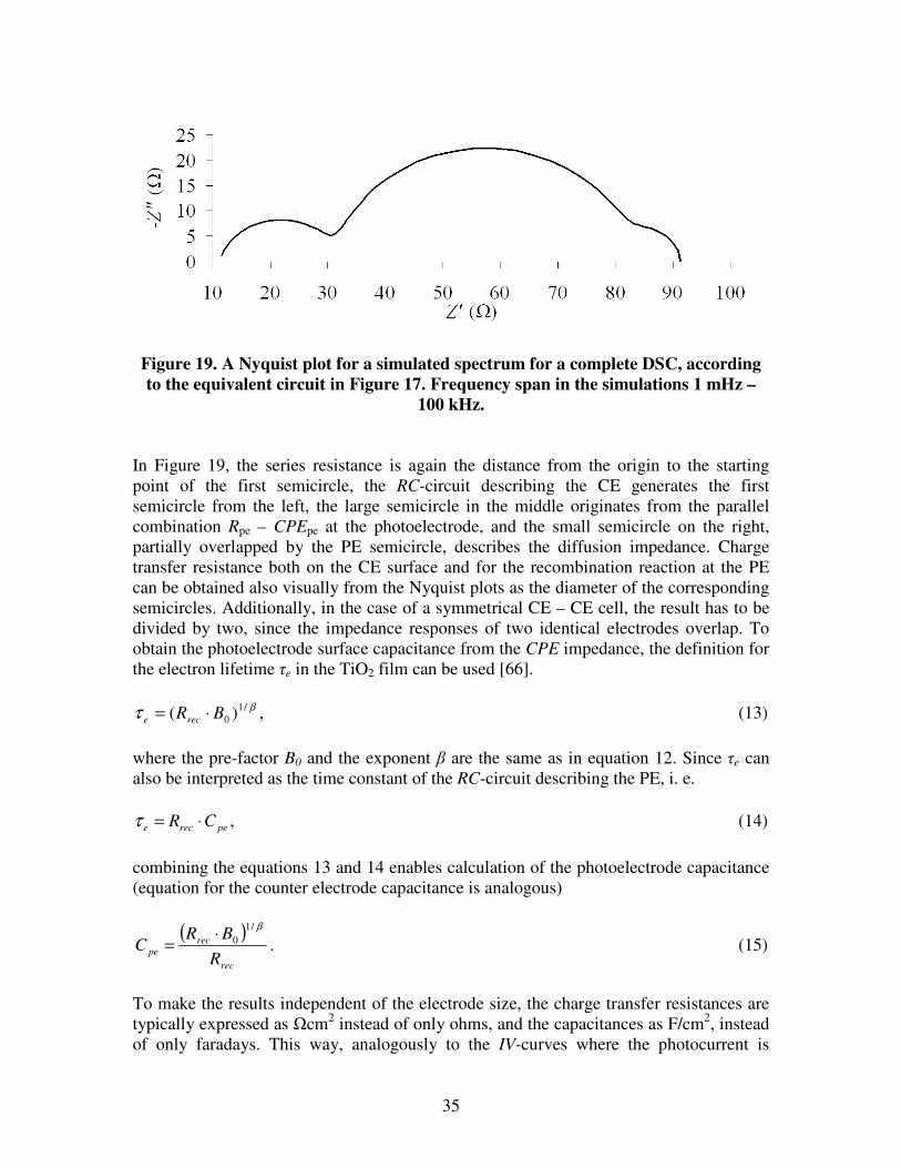
35
Figure 19. A Nyquist plot for a simulated spectrum for a complete DSC, according
to the equivalent circuit in Figure 17. Frequency span in the simulations 1 mHz –
100 kHz.
In Figure 19, the series resistance is again the distance from the origin to the starting
point of the first semicircle, the RC-circuit describing the CE generates the first
semicircle from the left, the large semicircle in the middle originates from the parallel
combination Rpe – CPEpe at the photoelectrode, and the small semicircle on the right,
partially overlapped by the PE semicircle, describes the diffusion impedance. Charge
transfer resistance both on the CE surface and for the recombination reaction at the PE
can be obtained also visually from the Nyquist plots as the diameter of the corresponding
semicircles. Additionally, in the case of a symmetrical CE – CE cell, the result has to be
divided by two, since the impedance responses of two identical electrodes overlap. To
obtain the photoelectrode surface capacitance from the CPE impedance, the definition for
the electron lifetime τe in the TiO2 film can be used [66].
βτ /1
0 )( BRrece ⋅= , (13)
where the pre-factor B0 and the exponent β are the same as in equation 12. Since τe can
also be interpreted as the time constant of the RC-circuit describing the PE, i. e.
perece CR ⋅=τ , (14)
combining the equations 13 and 14 enables calculation of the photoelectrode capacitance
(equation for the counter electrode capacitance is analogous)
( )
rec
rec
peR
BRC
β/1
0⋅= . (15)
To make the results independent of the electrode size, the charge transfer resistances are
typically expressed as Ωcm2 instead of only ohms, and the capacitances as F/cm
2, instead
of only faradays. This way, analogously to the IV-curves where the photocurrent is

36
expressed as A/cm2, the numerical values obtained are characteristic to the material, not
just a single cell.
If the electron transport resistance shows in the PE impedance response, it manifests itself
as a short, straight line of angle 45o between the CE and PE semicircles. In cases where
the transport resistance is so high that the electron diffusion length in the TiO2 film
remains shorter than the film thickness (i.e. high recombination probability and only a
small amount of photogenerated electrons can be collected), the whole PE semicircle
takes the shape characteristic to the Gerischer impedance and it becomes impossible to
define absolute values for either of the PE resistance components [67]. Figure 22 presents
examples of the DSC impedance spectra, where the transport resistance and Gerischer
impedance can be seen. In this kind of cases, where the PE impedance response is not a
“clean” semicircle, fitting the so-called transmission line element [67-69] to the PE
spectrum gives a more accurate result. In the transmission line model the transport
resistance in the TiO2 film, as well as the charge transfer resistance-capacitance
combination on the TiO2-electrolyte interface are modeled as a distribution of
infinitesimally small resistance and capacitance elements instead of one uniform value
describing the whole film or interface. Figure 20 presents a schematic of a pore in the
TiO2 film, modeled with the transmission line and Figure 21 a detailed, complete DSC
equivalent circuit where also the interfaces TiO2-substrate (Rco – CPEco) and electrolyte-
substrate (Rsu – CPEsu) are included. In practice, however, the impedance responses
originating from these interfaces occur on such frequencies that they get overlapped by
the more prominent CE and PE impedance arcs.
Figure 20. A schematic of a pore in the TiO2 film, described with the transmission
line model. rtr, rrec and cpepe are the distributed transport resistance, recombination
resistance and photoelectrode capacitance elements, respectively. Modified from the
picture presented in [67, 68].
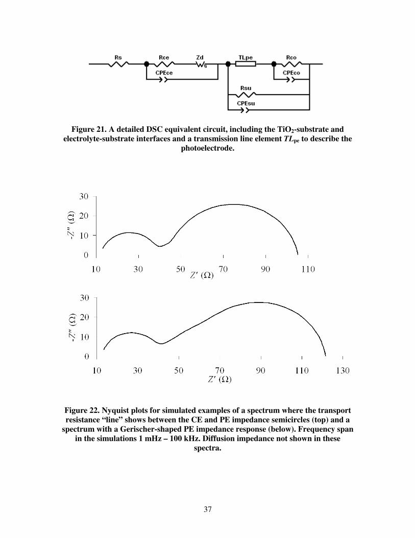
37
Figure 21. A detailed DSC equivalent circuit, including the TiO2-substrate and
electrolyte-substrate interfaces and a transmission line element TLpe to describe the
photoelectrode.
Figure 22. Nyquist plots for simulated examples of a spectrum where the transport
resistance “line” shows between the CE and PE impedance semicircles (top) and a
spectrum with a Gerischer-shaped PE impedance response (below). Frequency span
in the simulations 1 mHz – 100 kHz. Diffusion impedance not shown in these
spectra.

38
4 Experimental work
4.1 DSC materials and preparation
In the course of this thesis, the DSC preparation was investigated on ITO-PET and ITO-
PEN plastics, stainless steel, carbon steel and copper sheets and as a reference, FTO-
coated conducting glass substrates. Also, DSCs of cylindrical geometry were deposited
on glass and PMMA (polymethylmethacrylate) plastic optical fibers. ITO-PET (sheet
resistance 60 Ω/ and thickness 190 µm) was provided by Bekaert, Inc., ITO-PEN (sheet
resistance 15 Ω/) by Peccell, Inc., stainless steel (type 1.4301, thickness 0.8 – 1.25 mm)
by Outokumpu, Inc., carbon steels (both Zn-coated and plain, thickness 1 mm) by
Ruukki, Inc. and copper (thickness 0.63 mm) by Luvata, Inc. Fluorine-doped tin oxide
(FTO) glass (Pilkington TEC-8 with sheet resistance 8 Ω/ and thickness 3 mm and
Pilkington TEC-15 with sheet resistance 15 Ω/ and thickness 2.5 mm) was supplied by
Hartford Glass Company, Inc. Optical fibers were provided by Baltronic, Inc. (PMMA
plastic) and Photonium, Inc. (glass).
The pre-treatment of all substrates was similar: First, they were washed with warm water
and mild detergent, rinsed and let dry, after which the cleaning was finished in an
ultrasonic bath first three minutes in ethanol and then three minutes in acetone. After this,
the substrates were dried with pressurized air. The size of the substrates varied from the
16 mm x 20 mm for the small, laboratory-scaled test cells to 6 cm x 6 cm for the “mini-
modules” with which cell upscaling issues were studied.
Photoelectrodes were deposited both with doctor-blading method using commercial TiO2
paste (Sustainable Technologies International) and with spraying from self-made
suspension of 20 wt% TiO2 nanoparticles (P25 from Degussa) in absolute ethanol.
Doctor-blading was tried also with the suspension and since it worked well, this
deposition technique was adopted for low temperature photoelectrodes too. Since the
commercial paste requires sintering as post-treatment, it was obviously used only on
glass and metal substrates. Two or three layers of paste/suspension was spread through a
mask cut of regular office tape of 60 µm thickness. Between the layers, the substrates
were let to dry on a hot plate (100 – 110 oC) and in the case of the suspension, room
temperature compression in a hydraulic press (pressure 125 – 250 kg/cm2) was applied to
improve the particle adhesion on the substrate. As the final treatment, the glass and metal
photoelectrodes were sintered in 450 – 500 oC for half an hour and for the plastic
photoelectrodes, one final compression in the press was applied. The final thickness of
the TiO2 films was 10 – 15 µm. On the glass optical fibers the TiO2 was applied by
dipping the fibers into diluted TiO2 paste, after which the fibers were sintered
analogously to the glass substrates. On the plastic optical fibers, since compressing
cylindrical samples would have been difficult, the TiO2 layer (50 nm) was coated with
atomic layer deposition (ALD) method. Since the fiber substrates were not conductive as
such, a 130 nm of ZnO:Al was applied with the ALD prior to the TiO2 deposition. The
dye-sensitization of the photoelectrodes was done by soaking them in 0.32 mM
anhydrous ethanol solution of the N-719 dye (cis-bis(isothiocyanato)bis(2,2’-bipyridyl-

39
4,4’-dicarboxylato)-ruthenium(II) bis-tetrabutylammonium, Solaronix SA) for one day
minimum, after which the electrodes were rinsed and stored in absolute ethanol.
Platinized counter electrodes were prepared on glass, plastic and stainless steel substrates,
the glass ones being the reference against which the performance of the other types of
CEs were compared. On glass and steel, platinization was done with the standard thermal
method described in Chapter 2.4.4. Plastic substrates were platinized by sputtering. Since
Pt is an expensive CE catalyst, activated carbon and graphite based powder materials
were investigated as its replacement. Also, a platinized Sb:SnO2 powder was studied
since it is, like the carbon powders, possible to be applied without the high temperature
post-treatment and could thus be suitable also on plastic substrates. The compositions of
the carbon-based and platinized Sb:SnO2 powder materials were based on the literature,
and a modification of the activated carbon and graphite powder was successfully applied
also on the cylindrical DSCs on optical fibers. On planar substrates, the carbon and
Sb:SnO2 powder materials were deposited with the spraying method from ethanol-based
suspensions, analogously to the TiO2 suspensions. The mechanical integrity of the film
and its adherence to the substrate were achieved with room temperature compressing,
again analogously to the TiO2 powder photoelectrodes. The compression pressure for the
CEs was 1000 – 1500 kg/cm2.
The standard iodine electrolyte described in Chapter 2.4.3 was used in all cells prepared
for this study, the only variation being the iodine content which was optimized for the
electrolyte layer thickness. In some cases, the electrolyte was also gelatinized in order to
improve the mechanical strength of the electrolyte layer or its applicability, like in the
case of the optical fiber DSCs where all cell layers had to be deposited by the dipping
method. Before the electrolyte filling, the electrodes were sandwiched together on a hot
plate in 100 – 110 oC using a 25 µm or 45 µm thick Surlyn
® film as a spacer and sealant.
The electrolyte iodine content corresponding to these two spacer thicknesses was either
0.03 M or 0.05 M, respectively.
4.2 Cell characterization – measurements and equipment
The IV-curves were measured with a custom-made solar simulator equipped with ten 150
W halogen lamps as the irradiation source and a temperature-controlled measurement
plate on which the cell temperature could be adjusted to 25 oC. The irradiation intensity
was set to the standard 1000 W/m2 with a calibrated monocrystalline silicon reference
cell equipped with a spectral filter to mimic a typical DSC response. The mismatch factor
of the simulator was used to make the IV-curves correspond to the standard AM 1.5 G
solar spectrum. The optical fiber DSCs were measured either with side lighting in the
solar simulator or by coupling the light into the DSC fiber with a pigtail fiber.
The EIS data was recorded with Zahner Elektrik’s IM6 impedance measurement unit
operated with Thales software and the equivalent circuit fits were done with the ZView
software from Scribner, Inc. The cell lighting for the EIS measurements was provided
with a red LED of wavelength 640 nm and with the irradiation of ca. 8 % of one sun
intensity. To protect the cells from stray light, they and the LED were put inside a black

40
box for the measurements. For the temperature-ramped EIS measurements described in
Publication IV, the cells were put on a Pt-1000 temperature sensor controlled hot plate.
5 Results and discussion
5.1 Low temperature depositable counter electrodes for plastic substrates
(Publication I)
Whilst platinum still remains the most widely used and efficient CE catalyst in the DSC
and can be applied, in addition to the high temperature thermal method [46], also with
sputtering which is a suitable technique also for low temperature tolerance substrates
such as plastics, it is an expensive and, as a rare noble metal, not so abundant catalyst
material. Sputtering is also a technique which is difficult to integrate to continuous
throughput roll-to-roll type manufacturing process, it requires vacuum and wastes quite
much of the sputtered material, considering the sputtered layer forms not only on the
substrate but on the walls of the sputtering chamber as well. This is why, in order to
realize a fully flexible, cost-efficient and industrial-scale producable DSC, it is important
to find catalysts which are low price, easily available and depositable with industrially
upscaleable methods.
Several carbon-based materials have been presented in the literature, for example
activated carbons with different surface areas (carboxymethylcellulose as a binder) [70],
a mixture of carbon black and graphite (TiO2 nanoparticles as the binder) [71], and
single-wall carbon nanotubes [18] which, in addition to being an efficient catalyst for the
triiodide reduction reaction, have also low sheet resistance which could justify their use
not only as the catalyst but a replacement for the TCO coating of the substrate at the same
time. This is an interesting approach because the TCO coatings are expensive and, if the
coating and the catalyst could be deposited at the same manufacturing step, it would also
reduce the overall process time and costs. Carbon blacks have also been mixed into
composites with polymers [18] or used to improve the contact between the CE and the
solid-state DSC electrolyte [72]. The low price and easy availability of the activated
carbons and carbon blacks stems from their use in large production volumes in printing,
paint and pigment industries. Their catalytic efficiency is based on the small, nanoscale
particle size which increases the active surface area, yielding nanoporous electrodes not
quite unlike the nanocrystalline TiO2 on the photoelectrode side, whereas the function of
the graphite powder is to reduce the lateral resistance in the electrode film. However,
relatively thick layers (ten to several tens of µm) of the carbon-based materials are
needed in order to reach large enough active surface areas. This makes the electrode films
opaque (not suitable for cells where the lighting comes from the CE side, due to opaque
PE substrate such as metal sheets) and risks flaking of the electrode material in case the
cell is subject to bending. In addition to carbon materials, platinized Sb:SnO2
nanoparticle powder has also been successfully employed as the CE catalyst in the
literature [71].

41
In Publication I, the carbon black/graphite/TiO2 powder and platinized Sb:SnO2 powder
deposited on ITO-PET plastics were compared against thermally platinized FTO glasses
as DSC counter electrodes. To investigate the repeatability of the spray deposition and
room temperature compression method, large series (up to 200) of electrodes were
prepared and electrochemical impedance spectroscopy was employed as their
characterization method.
The carbon powder suspension for the spray deposition was prepared by grinding the
ingredients in a mortar in small amount of ethanol, after which more ethanol was added
in order to make the suspension fluid enough for spraying. Platinization of the Sb:SnO2
nanoparticles was realized by grinding the particles in a solution of Pt salt (PtCl4 in
isopropanol – the same solution used for the thermal platinization method) and firing the
resulting mixture in an oven in 385 oC for 10-15 minutes to achieve platinum’s reduction
from the solution and adherence to the Sb:SnO2 particles. After this, the resulting powder
was crushed and mixed with ethanol to a sprayable suspension as well. Spraying itself
was performed with an airbrush on heated substrates (ca. 100 oC) to ensure rapid
evaporation of the solvent and formation of even films, after which the films were
compressed in a hydraulic press in room temperature with pressures up to 1000 – 1500
kg/cm2. For the impedance measurements, symmetrical CE-CE cells were prepared
according to Figure 23.
Figure 23. A schematic of a symmetrical CE-CE cell [73].
The benefit of symmetrical CE-CE cells is that no impedance response originating from
the PE needs to be taken into account in the data analysis, i.e. the spectra are simpler,
consisting (ideally) only of one semicircle describing the charge transfer resistance –
capacitance parallel combination on the CE-electrolyte interface. Even the diffusion
impedance in the electrode could be neglected in these measurements, due to the porous
nature of the electrodes. Porosity increases the active surface area and thus the
capacitance of the electrode, which means that the porous electrode’s impedance appears

42
at lower frequencies compared to a planar electrode with the same charge transfer
resistance. This can be seen from the equation describing the characteristic frequency f*
of an RC-circuit
RCf
π2
1* = . (16)
In practice, the diffusion impedance arc got overlapped by the charge transfer impedance
arc in these measurements though on the other hand, an additional, parasitic impedance
arc was noticed (Figure 24).
Figure 24. Nyquist plots of typical impedance spectra of porous, compressed carbon
powder (∆) and platinized Sb:SnO2 powder () CEs [73].
The parasitic impedance arc on the left, high frequency end of the spectra in Figure 24
was deduced to originate from the bare ITO in contact with the electrolyte in the
electrolyte filling channels. At high frequencies, the electrode capacitance hinders the
current flow through the electrode-electrolyte interface but an alternative current pathway
originates from the parallel coupling of a part of the bare ITO’s resistance and the
capacitance on the ITO–electrolyte interface. The equivalent circuits in Figure 25
illustrate the situation: In Figure 25 b the cell series resistance Rs is divided in two parts
of which the component R2 describes the part of the ITO’s resistance which connects to
the ITO capacitance. When this impedance couples with the electrode impedance through
the ITO sheet resistance, it gives rise to the additional impedance arc in the spectra. To be
exact, the ITO resistance, capacitance and the RC-coupling of the electrode charge
transfer resistance and capacitance should be modeled with distributed elements, like in
the photoelectrode transmission line model described in Chapter 3.2 but the simplified
picture in Figure 25 illustrates the situation qualitatively enough. This theoretical
explanation for the additional impedance arc was also verified with tests where the bare
ITO in the electrolyte filling channels was electrically isolated from the ITO under the
electrode. No additional impedance arcs were noticed in these measurements, and the

43
“standard” CE-CE cell equivalent circuit in Figure 25 a could be used for the data fits for
these cells. However, the appearance of the parasitic impedance underlines careful design
of the measurement cells and non-uniform, distributed nature of the cell series resistance.
Figure 25. Equivalent circuits used for the data fits in Publication I. a: the
“standard” CE-CE cell circuit. b: the circuit for the case where the bare ITO
resistance in the electrolyte filling channels couples with the ITO capacitance [73].
The performance of the carbon powder electrodes, characterized with the charge transfer
resistance, was very good. With 10-20 µm thick electrodes, charge transfer resistances of
0.5-2 Ωcm2 were measured, which is even lower than the 4-5 Ωcm
2 obtained with
thermally platinized FTO glasses in this study and well comparable to results reported for
sputtered platinum electrodes in the literature, 0.8-2.1 Ωcm2 [42, 74, 75]. For the
platinized Sb:SnO2, the charge transfer resistances were somewhat higher, 8-13 Ωcm2 for
20-40 µm thick layers, though when proportioned to the Pt loading in these films which
corresponds to 1.1-2.3 nm of planar Pt layer, this result is also well comparable to e.g.
sputtered Pt films [42, 74, 75]. The repeatability of the spray deposition and compression
method was good, yielding large series of even quality electrodes with high speed. The
mechanical stability of the Sb:SnO2 films was better than that of the carbon powder films
– it was noticed that when the film thickness exceeded 40 µm, carbon films tended to
flake off. Also, long enough grinding of the carbon powder suspension ingredients
proved to be crucial for high quality electrodes: Less than 15 minutes grinding yielded
electrodes with charge transfer resistances from 70 Ωcm2 to several hundreds of Ωcm
2
and also poorer adherence to the substrate.
All in all, spray and compression depositable powder materials seemed promising
alternatives to Pt in flexible DSCs manufactured with high throughput roll-to-roll
methods. Mechanical stability and qualitative evenness of the films was satisfactory for
small, laboratory-scale test cells but in order to drastically increase the cell size,

44
additional stability-improving agents such as binders need to be mixed into the material
to improve the interparticle contacts and adherence to the substrate.
5.2 Preliminary tests on industrial sheet metals for DSC substrates (Publication
II)
In addition to plastics, metal materials are another group of substrates that could realize
both flexible and cost-efficient DSC. The underlying motive in Publication II was to
investigate if common industrial sheet metals such as carbon or stainless steels (StS)
could be used as the DSC substrates as such. With this approach, the DSC could work as
a light-active functional coating on top of the metal sheet realizing for example roofing
and façade materials that would produce electricity at the same time. This kind of
building materials would save the costs of additional supporting structures of the PV
panels, thus facilitating easy installation and implementation of solar electricity and also
widen the product variety of metal industries.
Compared to glass and plastics, metals have been studied relatively little as DSC
substrates [e.g. 19-27]. In this study, the suitability of several types of Zn-coated and
plain carbon steels, stainless steel and copper in this function was preliminarily
investigated with soaking and encapsulation tests. In soaking tests, small pieces of the
metal materials were immersed in the standard liquid iodine electrolyte described in
chapter 2.3.3 and in encapsulation tests, a small amount of the electrolyte was sealed
between the metal sheet and glass in order to mimic more closely the situation in the real
cell. The soaking test samples were stored in outdoor light, room light or dark to see if
lighting conditions had any effect on the behavior of the metals in the electrolyte, and
after several weeks the metal ion concentrations in the electrolyte were measured with
atomic absorption spectrometry.
Of the studied metal materials, only stainless steel showed sufficient stability in the
electrolyte to be employed as DSC substrate as such. The main problem concerning metal
substrates in the case of the DSC is the iodine electrolyte since, according to reaction
−+− +→+ IMIM 32
3 , (17)
where M = arbitrary metal atom/ion, triiodide ions are corrosive towards most metals.
Since the triiodide ions give to the electrolyte its distinctive dark reddish color but the
iodide ions are colorless, the reaction shown in (17) turned out to be also an easy visual
way to inspect the stability of metals in the presence of the electrolyte. For example, in
the encapsulation tests, the dark reddish color disappeared in only a few seconds when
the electrolyte was encapsulated against a copper sheet. The Zn-coated carbon steel
samples corroded relatively fast also, in only a few hours. Oxidizing the Zn-coatings in
an oven in 600 oC was tried in order to make the coatings more resistive towards
corrosion (metal oxides are usually more stable than pure metals and ZnO electrodes
have been employed in the DSC [e.g. 76]) but not even this treatment could prolong the
stability to more than one day maximum. Compact, spray-pyrolyzed TiO2 and ITO thin

45
films were also investigated as corrosion protection coatings but obviously the films had
so much microscale porosity that they did not noticeably improve the metal samples’
stability. In the soaking tests, the electrolyte color started to fade in only a few days in the
presence of Zn-coated carbon steels or copper (Figure 26). Surprisingly, plain carbon
steel showed somewhat better stability, the complete disappearance of the electrolyte
color in the encapsulation tests not occurring until after two months. For stainless steel
samples, no visual signs of corrosion or metal ions in the electrolyte could be detected
even after 12 months of exposure to the electrolyte.
Figure 26. The gradual fading of the electrolyte color in the presence of a corroding
metal sample. Left: initial color; right: final color [22].
Based on the soaking and encapsulation tests, stainless steel and carbon steel were chosen
for further studies. The metal sheets were employed as counter electrodes and their
performance characterized with impedance spectroscopy and with IV-curve
measurements from complete DSCs.
Plain metal sheets showed no catalytic activity at all, their charge transfer resistances
being of the order 103 – 10
13 Ωcm
2, which is why they were platinized with the thermal
method analogously to TCO glass substrates. After platinization, charge transfer
resistances around 20 Ωcm2 were achieved, yielding cells with 3.6 % efficiency with a
stainless steel CE and glass PE and 3.1 % with a carbon steel CE and glass PE (cf. 4.6 %
with an all-glass cell in this study). The series resistances of the cells were only 2 Ω (with
glass cells typically around 10 Ω), which is due to the steel substrates’ superior
conductivity (sheet resistances of metal materials are of the order mΩ/). In the literature,
at the time of this research, 4-5 % efficiencies were obtained with platinized stainless
steel and nickel CEs though not all of the results are directly comparable since additional
oxide layers were deposited on top of the steel in some of these studies [20, 21, 77].
Other platinization methods than the thermal deposition were also used which may have
resulted in different quality, microstructure and morphology of the Pt films.
Despite the promising efficiencies, the fill factors of the stainless steel and carbon steel
CE cells were relatively low, ca. 35 %, which indicates high resistive losses somewhere

46
in the cell, even in spite of the metal substrate’s high conductivity. Platinum’s poorer
adhesion to the metals, compared to TCO glass (the platinum layer could be partially
detached from the metal sheet by melting a Surlyn film on top of it and pulling it off)
might give rise to additional contact resistance between the Pt layer and metal substrate
and thus contribute to the overall ohmic losses as well.
Since plain, uncoated carbon steel is not a suitable building material in reality, based on
the results in Publication II stainless steel was chosen as the metal substrate for closer
studies.
5.3 Further studies on the suitability of metal materials for DSC substrates
(Publications V and VII)
Even if promising efficiencies were measured with the stainless steel CE DSCs, the
problem with this cell design is that in order to keep the cell structure completely flexible,
the photoelectrode has to be deposited on plastic. Whilst it is possible to prepare
satisfactory quality cells with plastic PEs, the mechanical stability and electron transport
properties of a compressed-only TiO2 film are not as good as those of a high-temperature
sintered electrode, which is why a reverse design, where the PE is prepared on the steel
sheet and the CE on plastic (as a reference also on glass), was developed. Steel substrate
tolerates high temperatures, which enables sintering of the PE films and due to its
superior electrical conductivity, it is also a promising substrate material for cell size
upscaling. Flexible CEs with high catalytic activity and good mechanical and chemical
stability, on the other hand, are relatively easy to prepare for example with sputtering
platinum on ITO-PET. Figure 27 presents schematics of the stainless steel based DSC
geometries.
Figure 27. StS-based DSC designs. StS as the PE (upper, here with a PEDOT CE)
and as the CE (lower) [78].
The obvious problem in the reverse cell design where light has to enter the photoactive
material through CE and electrolyte layers due to the opaqueness of the steel substrate is
light absorption in these layers. This shadowing effect can be minimized, though, with
optimization of the cell structure.
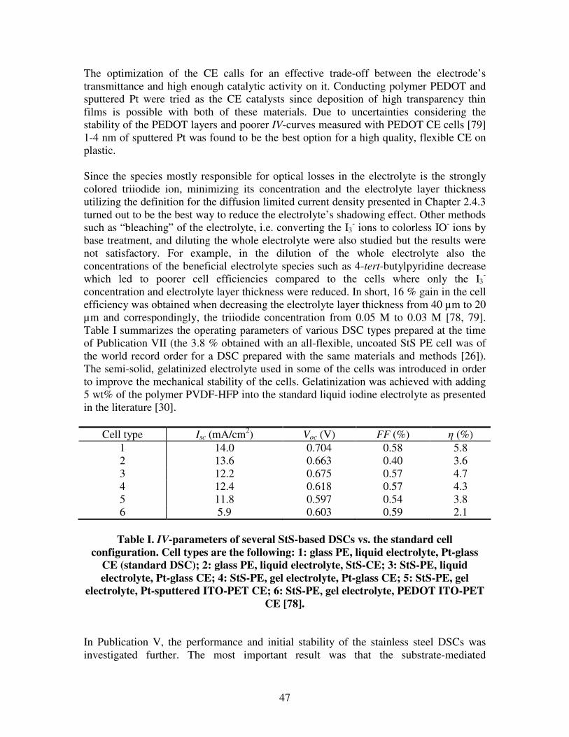
47
The optimization of the CE calls for an effective trade-off between the electrode’s
transmittance and high enough catalytic activity on it. Conducting polymer PEDOT and
sputtered Pt were tried as the CE catalysts since deposition of high transparency thin
films is possible with both of these materials. Due to uncertainties considering the
stability of the PEDOT layers and poorer IV-curves measured with PEDOT CE cells [79]
1-4 nm of sputtered Pt was found to be the best option for a high quality, flexible CE on
plastic.
Since the species mostly responsible for optical losses in the electrolyte is the strongly
colored triiodide ion, minimizing its concentration and the electrolyte layer thickness
utilizing the definition for the diffusion limited current density presented in Chapter 2.4.3
turned out to be the best way to reduce the electrolyte’s shadowing effect. Other methods
such as “bleaching” of the electrolyte, i.e. converting the I3- ions to colorless IO
- ions by
base treatment, and diluting the whole electrolyte were also studied but the results were
not satisfactory. For example, in the dilution of the whole electrolyte also the
concentrations of the beneficial electrolyte species such as 4-tert-butylpyridine decrease
which led to poorer cell efficiencies compared to the cells where only the I3-
concentration and electrolyte layer thickness were reduced. In short, 16 % gain in the cell
efficiency was obtained when decreasing the electrolyte layer thickness from 40 µm to 20
µm and correspondingly, the triiodide concentration from 0.05 M to 0.03 M [78, 79].
Table I summarizes the operating parameters of various DSC types prepared at the time
of Publication VII (the 3.8 % obtained with an all-flexible, uncoated StS PE cell was of
the world record order for a DSC prepared with the same materials and methods [26]).
The semi-solid, gelatinized electrolyte used in some of the cells was introduced in order
to improve the mechanical stability of the cells. Gelatinization was achieved with adding
5 wt% of the polymer PVDF-HFP into the standard liquid iodine electrolyte as presented
in the literature [30].
Cell type Isc (mA/cm2) Voc (V) FF (%) η (%)
1 14.0 0.704 0.58 5.8
2 13.6 0.663 0.40 3.6
3 12.2 0.675 0.57 4.7
4 12.4 0.618 0.57 4.3
5 11.8 0.597 0.54 3.8
6 5.9 0.603 0.59 2.1
Table I. IV-parameters of several StS-based DSCs vs. the standard cell
configuration. Cell types are the following: 1: glass PE, liquid electrolyte, Pt-glass
CE (standard DSC); 2: glass PE, liquid electrolyte, StS-CE; 3: StS-PE, liquid
electrolyte, Pt-glass CE; 4: StS-PE, gel electrolyte, Pt-glass CE; 5: StS-PE, gel
electrolyte, Pt-sputtered ITO-PET CE; 6: StS-PE, gel electrolyte, PEDOT ITO-PET
CE [78].
In Publication V, the performance and initial stability of the stainless steel DSCs was
investigated further. The most important result was that the substrate-mediated
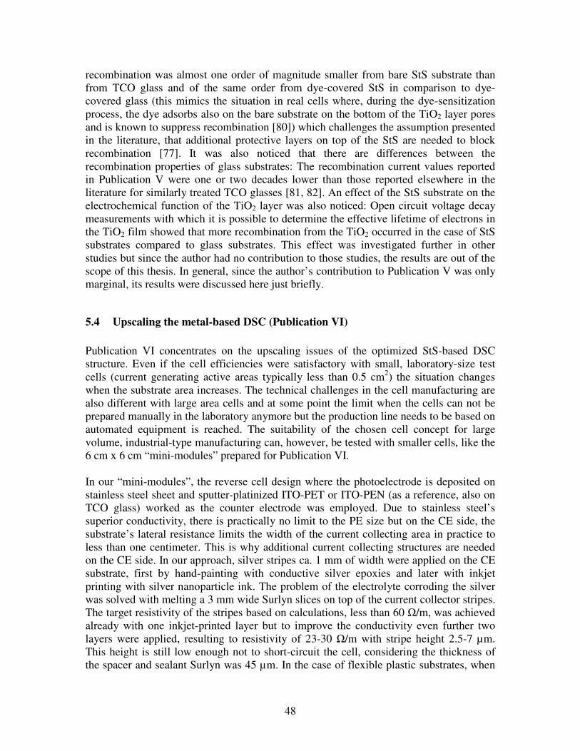
48
recombination was almost one order of magnitude smaller from bare StS substrate than
from TCO glass and of the same order from dye-covered StS in comparison to dye-
covered glass (this mimics the situation in real cells where, during the dye-sensitization
process, the dye adsorbs also on the bare substrate on the bottom of the TiO2 layer pores
and is known to suppress recombination [80]) which challenges the assumption presented
in the literature, that additional protective layers on top of the StS are needed to block
recombination [77]. It was also noticed that there are differences between the
recombination properties of glass substrates: The recombination current values reported
in Publication V were one or two decades lower than those reported elsewhere in the
literature for similarly treated TCO glasses [81, 82]. An effect of the StS substrate on the
electrochemical function of the TiO2 layer was also noticed: Open circuit voltage decay
measurements with which it is possible to determine the effective lifetime of electrons in
the TiO2 film showed that more recombination from the TiO2 occurred in the case of StS
substrates compared to glass substrates. This effect was investigated further in other
studies but since the author had no contribution to those studies, the results are out of the
scope of this thesis. In general, since the author’s contribution to Publication V was only
marginal, its results were discussed here just briefly.
5.4 Upscaling the metal-based DSC (Publication VI)
Publication VI concentrates on the upscaling issues of the optimized StS-based DSC
structure. Even if the cell efficiencies were satisfactory with small, laboratory-size test
cells (current generating active areas typically less than 0.5 cm2) the situation changes
when the substrate area increases. The technical challenges in the cell manufacturing are
also different with large area cells and at some point the limit when the cells can not be
prepared manually in the laboratory anymore but the production line needs to be based on
automated equipment is reached. The suitability of the chosen cell concept for large
volume, industrial-type manufacturing can, however, be tested with smaller cells, like the
6 cm x 6 cm “mini-modules” prepared for Publication VI.
In our “mini-modules”, the reverse cell design where the photoelectrode is deposited on
stainless steel sheet and sputter-platinized ITO-PET or ITO-PEN (as a reference, also on
TCO glass) worked as the counter electrode was employed. Due to stainless steel’s
superior conductivity, there is practically no limit to the PE size but on the CE side, the
substrate’s lateral resistance limits the width of the current collecting area in practice to
less than one centimeter. This is why additional current collecting structures are needed
on the CE side. In our approach, silver stripes ca. 1 mm of width were applied on the CE
substrate, first by hand-painting with conductive silver epoxies and later with inkjet
printing with silver nanoparticle ink. The problem of the electrolyte corroding the silver
was solved with melting a 3 mm wide Surlyn slices on top of the current collector stripes.
The target resistivity of the stripes based on calculations, less than 60 Ω/m, was achieved
already with one inkjet-printed layer but to improve the conductivity even further two
layers were applied, resulting to resistivity of 23-30 Ω/m with stripe height 2.5-7 µm.
This height is still low enough not to short-circuit the cell, considering the thickness of
the spacer and sealant Surlyn was 45 µm. In the case of flexible plastic substrates, when

49
the free area between the Surlyn seals widens to near one cm, the capillary forces tend to
bend the plastic in the middle, thus risking the substrates touching each other which is
why thicker spacer films are needed for larger area cells. Optical losses in a reverse
lighting, thicker spacer cells are also compensated some since the front (plastic)
substrate’s bending diminishes the distance between the electrodes.
To optimize the large cell structure, i.e. the positioning and geometry of the CE current
collector stripes and correspondingly, the width of the TiO2 stripes on the PE side, a
semi-empirical mathematical model was developed [83]. The model was based on partial
differential equations describing the current flow in the cell, special emphasis being put
on the counter electrode – electrolyte interface. The model was constructed and solved
with COMSOL Multiphysics©
software and its input consisted of a measured IV-curve of
a small, laboratory-size test cell and the data about the spatial distribution of the substrate
surface conductivities, depending on the substrate material and the location of the current
collector structures. The current generation on the PE side was modeled with an
“extended” dye solar cell equivalent circuit (Figure 28), as a parallel combination of a
photocurrent source term (Iph) and a diode (Id) describing the recombination current. In
another words, the large cell was treated as an “infinite” number of infinitesimally small
cells in parallel. With the model, the voltage losses in different parts of the large cell
could be calculated (Figure 29) and the structure optimized to minimize those, along with
the active area losses bound to occur because of the current collector positioning and
protection. Figure 30 presents schematics of the two final large cell configurations, one
for cells with TCO glass CE (reference) and another for cells with ITO-PET CE, and
Figure 31 photographs of the real cells. In the ITO-PET CE cells, the silver stripes are
widened slightly near the main current collector to reduce the ohmic losses due to
substrate’s sheet resistance as much as possible.
Figure 28. An “extended” DSC equivalent circuit used to model the current
generation and voltage losses in a large cell [83].

50
Figure 29. Current densities and voltage losses in a 6 cm x 6 cm DSC “mini-
module”. In the picture, the main current collector is located on top of the picture
which is why the current flow is the most efficient there [83].
Figure 30. The final geometries for the large cell. On the left for the glass CE cells,
on the right for the ITO-PET CE cells. Dark red: dyed TiO2; light grey: silver
stripes. Active areas on both cell types ca. 15 cm2 [83].
Figure 31. Photographs of StS-based DSC “mini-modules”, substrate size 6 cm x 6
cm.
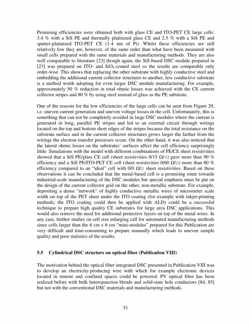
51
Promising efficiencies were obtained both with glass CE and ITO-PET CE large cells:
3.4 % with a StS PE and thermally platinized glass CE and 2.5 % with a StS PE and
sputter-platinized ITO-PET CE (1-4 nm of Pt). Whilst these efficiencies are still
relatively low they are, however, of the same order than what have been measured with
small cells prepared with the same materials and manufacturing methods. They are also
well comparable to literature [23] though again, the StS-based DSC module prepared in
[23] was prepared on ITO- and SiOx-coated steel so the results are comparable only
order-wise. This shows that replacing the other substrate with highly conductive steel and
embedding the additional current collector structures to another, less conductive substrate
is a method worth adopting for even larger DSC module manufacturing. For example,
approximately 50 % reduction in total ohmic losses was achieved with the CE current
collector stripes and 80 % by using steel instead of glass as the PE substrate.
One of the reasons for the low efficiencies of the large cells can be seen from Figure 29,
i.e. uneven current generation and uneven voltage losses in the cell. Unfortunately, this is
something that can not be completely avoided in large DSC modules where the current is
generated in long, parallel PE stripes and led to an external circuit through wirings
located on the top and bottom short edges of the stripes because the total resistance on the
substrate surface and in the current collector structures grows larger the farther from the
wirings the electron transfer processes occur. On the other hand, it was also noticed that
the lateral ohmic losses on the substrates’ surfaces affect the cell efficiency surprisingly
little: Simulations with the model with different combinations of PE/CE sheet resistivities
showed that a StS PE/glass CE cell (sheet resistivities 0/15 Ω/) gave more than 90 %
efficiency and a StS PE/ITO-PET CE cell (sheet resistivities 0/60 Ω/) more than 80 %
efficiency compared to an “ideal” cell with 0/0 Ω/ sheet resistivities. Based on these
observations it can be concluded that the metal-based cell is a promising route towards
industrial-scale manufacturing of the DSC modules but special emphasis must be put on
the design of the current collector grid on the other, non-metallic substrate. For example,
depositing a dense “network” of highly conductive metallic wires of micrometer scale
width on top of the PET sheet under the ITO coating (for example with inkjet-printing
methods; the ITO coating could then be applied with ALD) could be a successful
technique to prepare high quality CE substrates for large area DSC applications. This
would also remove the need for additional protective layers on top of the metal wires. In
any case, further studies on cell size enlarging call for automated manufacturing methods
since cells larger than the 6 cm x 6 cm “mini-modules” prepared for this Publication are
very difficult and time-consuming to prepare manually which leads to uneven sample
quality and poor statistics of the results.
5.5 Cylindrical DSC structure on optical fiber (Publication VIII)
The motivation behind the optical fiber integrated DSC presented in Publication VIII was
to develop an electricity-producing wire with which for example electronic devices
located in remote and confined spaces could be powered. PV optical fiber has been
realized before with bulk heterojunction blends and solid-state hole conductors [84, 85]
but not with the conventional DSC materials and manufacturing methods.

52
Cylindrical geometry and the non-conductive surface of the fibers obviously present
some manufacturing challenges though the latter was easy to overcome with depositing a
conductive oxide coating on the fibers with the ALD method. The same method had to be
applied also when depositing the TiO2 layer on PMMA plastic optical fibers since they
can not tolerate temperatures much higher than 80 oC so sintering as the TiO2 film post-
treatment could not be used. Since the ALD method yields only compact thin films
(several tens of nanometers thick) the ALD-deposited PE could obviously not produce
currents comparable to proper nanoporous, high active surface area TiO2 films. The idea
could be demonstrated even with this thin TiO2 layer, though, and on glass fibers a
“normal”, sintered PE could be prepared with dip-coating from diluted titania paste.
PVDF-HFP gelatinized iodine electrolyte [30] which turns liquid when heated to 130 -
140 oC but solidifies when cooled again to room temperature was a feasible option to coat
the electrolyte layer on top of the dye-sensitized PE and for the counter electrode, a new,
gelatinized carbon material was developed. This material was based on the carbon
black/graphite/TiO2 powder suspension described earlier in chapter 4.1 and Publication I.
To make the material suitable for dip-coating it was gelatinized with PVDF-HFP. To
enable heating of the mixture to 130 – 140 oC needed to liquefy the gel, the normally
used ethanol was replaced with 3-methoxypropionitrile (MePRN) as the suspension
solvent (the boiling point of MePRN is so high that it doesn’t vaporize when the gel is
heated up, in contrast to ethanol which boils already under 100 oC). This gelatinized
carbon powder suspension solidified into hard, sturdy films on top of the fiber which
enabled application of the current collector contacts and handling of the fibers without
risking the counter electrode layer flaking off. Actually, the carbon gel looks like a
promising alternative as a low temperature depositable CE material for planar cells as
well since even plastic substrates can take temperatures up to 130 – 140 oC. The polymer
networks inside the CE film improve the mechanical stability of it, making it more
“flexible” and tolerable to cell bending. They also “bind” the individual particles of the
powder together more efficiently than compressing only, so even thicker CE films with
higher catalytic activity could be prepared. Due to its viscosity, the heated gel is also easy
to apply with doctor-blading/screen-printing method. Figure 32 presents a schematic of
the optical fiber DSC.
Even though the cell manufacturing was possible even on cylindrical substrate such as
the fibers, the photocurrents remained on the nA scale and correspondingly, cell
efficiencies extremely low. With plastic fibers this is easy to understand because only a
very small amount of dye can adsorb on an ALD-coated TiO2 film and with glass fibers,
obviously further optimization of the PE film depositing process is called for to improve
the film structure, morphology and adhesion to the fiber. However, the open circuit
voltages measured from the fiber DSCs were of the same order than those typically
obtained with planar cells: 0.5 V at its best (cf. 0.65 – 0.70 V for planar cells). This
indicates that despite the low efficiencies, this kind of a DSC could work for example as
a photoactive sensor, monitoring the light propagation in an optical fiber. For final
applications, the DSC should also be encapsulated with a film that prevents both moisture
penetration into the structure and drying of the electrolyte solvent. Even if the gelatinized
electrolyte is solid in room temperatures, the polymer forms only a loose network around
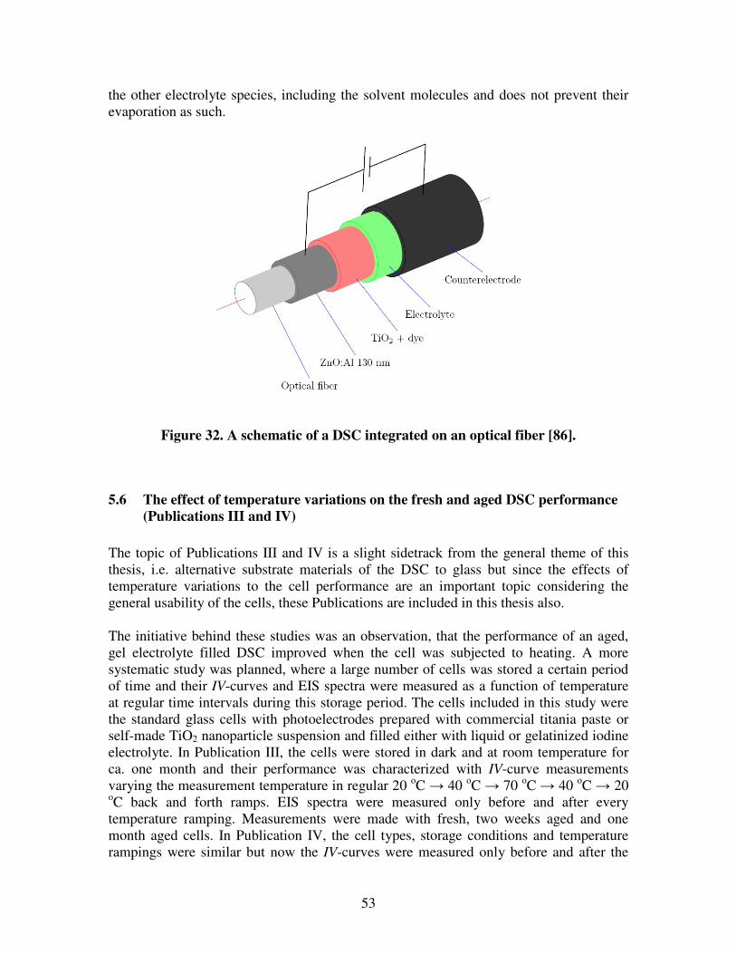
53
the other electrolyte species, including the solvent molecules and does not prevent their
evaporation as such.
Figure 32. A schematic of a DSC integrated on an optical fiber [86].
5.6 The effect of temperature variations on the fresh and aged DSC performance
(Publications III and IV)
The topic of Publications III and IV is a slight sidetrack from the general theme of this
thesis, i.e. alternative substrate materials of the DSC to glass but since the effects of
temperature variations to the cell performance are an important topic considering the
general usability of the cells, these Publications are included in this thesis also.
The initiative behind these studies was an observation, that the performance of an aged,
gel electrolyte filled DSC improved when the cell was subjected to heating. A more
systematic study was planned, where a large number of cells was stored a certain period
of time and their IV-curves and EIS spectra were measured as a function of temperature
at regular time intervals during this storage period. The cells included in this study were
the standard glass cells with photoelectrodes prepared with commercial titania paste or
self-made TiO2 nanoparticle suspension and filled either with liquid or gelatinized iodine
electrolyte. In Publication III, the cells were stored in dark and at room temperature for
ca. one month and their performance was characterized with IV-curve measurements
varying the measurement temperature in regular 20 oC → 40
oC → 70
oC → 40
oC → 20
oC back and forth ramps. EIS spectra were measured only before and after every
temperature ramping. Measurements were made with fresh, two weeks aged and one
month aged cells. In Publication IV, the cell types, storage conditions and temperature
rampings were similar but now the IV-curves were measured only before and after the
54
temperature treatments whereas the EIS spectra were recorded at every ramp temperature
with fresh, ca. two weeks, ca. one month and two and half months aged cells. Also, to
uncouple the effect of temperature on the open circuit voltage another set of impedance
measurements was performed, where the cell voltage was fixed to 0.6 V, 0.65 V, 0.7 V
and 0.75 V with external polarization and the EIS spectra recorded in all those voltages
varying the temperature in every voltage in similar ramps as described before. These
measurements were performed on one day only.
The most important finding in Publication III was that the overall drop in the efficiency
was smaller for temperature-ramped cells than for reference cells that were stored in
similar conditions and for the same time and measured at the same days than the
temperature-ramped cells but only at room temperature. When averaged over the four
different cell types prepared for this study, the efficiency drop was 18 %-unit less for the
temperature-treated cells. The most prominent reason for the efficiency degradation over
time was decrease in short circuit current whereas the open circuit voltage remained
almost the same over the whole observation period. The best cell performance was
obtained at 40 oC though when the temperature was increased to 70
oC, a radical drop
both in Isc and Voc happened. This drop was reversible, though, and when the temperature
was lowered in the downward sweep of the ramp, the currents set on higher level than
what they had been on in the upward sweep. Actually, the currents remained on this
higher level still on the next consecutive measurement day. Figure 33 presents examples
of the IV-curves before and after the temperature treatments for ca. two weeks aged cells.
Figure 33. IV-curves of ca. two weeks aged cell, before and after the temperature
ramping treatment. Left: liquid electrolyte filled cell; right: gel electrolyte filled cell
[87].
From the EIS data it could be detected that the electron lifetimes τel in the TiO2 film were
longer and the charge transfer resistance on the counter electrode lower after the
temperature rampings. This can be seen also from Figure 34, where the CE impedance
arc in the Nyquist plot is clearly smaller after the temperature treatment and the
characteristic frequency of the PE impedance response (i.e. the frequency of the

55
imaginary impedance peak’s maximum) in the Bode plot moves to smaller frequencies f
according to equation [16]
fe
πτ
2
1≈ . (18)
Figure 34. Impedance responses of fresh and ca. one month aged (gel electrolyte
filled) cells, before and after the temperature ramping treatment. Top: Nyquist
plots; bottom: Bode plots. In the Nyquist plots, the semicircle on the left originates
from the CE and the one on the right from the PE. Diffusion impedance arc is halfly
overlapped by the PE arc. In the Bode plots, the imaginary impedance peak and the
sharp rise in the real impedance on the left originate from the PE and the
corresponding characteristics on the right from the CE [87].

56
The effect of temperature on the CE function also showed some permanence, the charge
transfer resistances staying on this lower level even a few hours after the temperature
rampings were made. The improvement in the CE catalyst function in elevated
temperatures is easy to understand because most catalytes work more efficiently in higher
temperatures but the electron lifetime lengthening was a somewhat surprising result. This
indicates that the temperature rampings had a positive effect on the recombination
suppressing properties of the TiO2-electrolyte interface – even though as a function of
time only, the recombination was noticed to increase. The CE charge transfer resistance
increased also as a function of time, indicating deterioration in the CE catalyst. However,
the regenerating effect the temperature rampings had on the overall cell performance
indicates that instead of being detrimental to the cell operation and long term stability,
regularly varying temperature might instead improve those, taken that the temperature
does not exceed ca. 60 oC for extended periods of time. The CE regeneration in the
temperature rampings also agrees with [89], where two days of thermal aging improved
the CE performance.
The results of Publication IV reflected the results obtained in Publication III. i.e. the
aging- and temperature-induced changes in the overall cell performance and the counter
electrode function were similar. Due to more detailed EIS measurements, however, more
data especially about the behavior of the PE resistance and capacitance could be obtained.
For example, it could be detected that the electron transport resistance in the PE film
increased over time which indicates deterioration in the PE quality, most likely in
interparticle contacts, and that this effect was accentuated at elevated temperatures. This
can be seen even visually from Figure 35, where the PE impedance arc of an aged cell
undergoes a gradual change from a “clean” semicircle to the Gerischer-shape when the
temperature is increased from 20 oC to 70
oC. Also, the transport resistance “line”
between the PE and CE arcs can clearly be seen in the aged cell’s spectrum measured at
40 oC. In these measurements it must be noted, however, that because the cell voltage
was not externally controlled, the Voc was free to vary according to temperature. As the
Voc decreases when the temperature increases the increase in Rtr (and also in Rrec) reflects
this. When the Voc is low there are less electrons in the TiO2 film which hinders efficient
charge transport, thus resulting in higher Rtr.
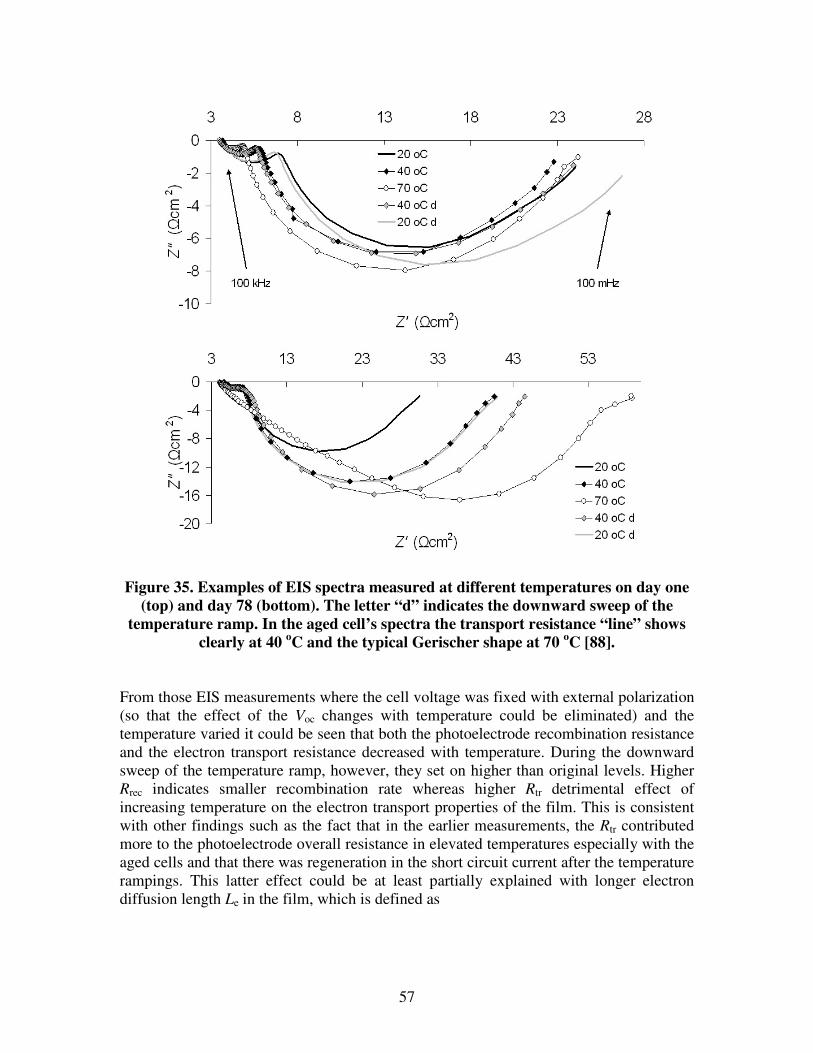
57
Figure 35. Examples of EIS spectra measured at different temperatures on day one
(top) and day 78 (bottom). The letter “d” indicates the downward sweep of the
temperature ramp. In the aged cell’s spectra the transport resistance “line” shows
clearly at 40 oC and the typical Gerischer shape at 70
oC [88].
From those EIS measurements where the cell voltage was fixed with external polarization
(so that the effect of the Voc changes with temperature could be eliminated) and the
temperature varied it could be seen that both the photoelectrode recombination resistance
and the electron transport resistance decreased with temperature. During the downward
sweep of the temperature ramp, however, they set on higher than original levels. Higher
Rrec indicates smaller recombination rate whereas higher Rtr detrimental effect of
increasing temperature on the electron transport properties of the film. This is consistent
with other findings such as the fact that in the earlier measurements, the Rtr contributed
more to the photoelectrode overall resistance in elevated temperatures especially with the
aged cells and that there was regeneration in the short circuit current after the temperature
rampings. This latter effect could be at least partially explained with longer electron
diffusion length Le in the film, which is defined as

58
dR
RL
tr
rec
e ⋅= , (19)
where d is the film thickness. Longer diffusion length improves the probability that the
electrons reach the current collector before recombination, thus increasing the Isc.
However, in general the temperature-induced variation in Le was quite small and irregular
in this study so probably other factors than only that were responsible for the Isc
regeneration. Le’s temperature behavior was also contradictory to what had been
published previously in [68] though it must be noted here that the measurements in [68]
were made in the dark whereas our measurements were performed with lighted cells. The
temperature behavior of PE capacitance contradicted results in [68] also – in [68] the Cpe
was independent of temperature whereas in our experiments, clear (and reversible)
increase as a function of temperature was observed. This is in agreement with other
publications though, namely [14], where the cells were also measured when lighted.
Because the lighting conditions only affect the direction from which the electrons are
injected to the PE film (in dark they come from the external circuit and in light, from the
dye) where their total amount then sets the Voc which directly affects the capacitance the
fact that the capacitance shows temperature dependence only when the electrons come
from the dye indicates temperature-dependent changes in the dye-TiO2 interface or the
structure/properties of the dye itself. Cpe’s temperature behavior at fixed voltages, when
plotted against 1/T, also indicates temperature-induces shifts in the TiO2 conduction band
energy level and/or redox Fermi level which would also agree with [14].
6 Summary and conclusions
In order to utilize solar electricity’s full potential as a clean, renewable energy source
new PV device concepts have to be developed alongside the already established,
traditional silicon and thin film panels. This thesis concentrates on dye solar cells, a still
relatively new type of photovoltaic converter, which promises lie in for the most part
cheap, non-toxic and well abundant materials and simple manufacturing methods.
However, since the common approach has been to prepare dye solar cells on glass
alternative substrate materials need to be found. Whilst glass DSC still gives the highest
efficiencies and best results concerning long term stability of the cells, rigid and fragile
glass substrate is obviously suitable only for batch process type manufacturing, quite like
the silicon and thin film panels as well.
In this thesis alternative substrate materials to glass, namely ITO-PET plastic foils and
stainless steel sheets have been investigated. Preparing the cells on flexible, light weight
substrates such as plastics enables high throughput roll-to-roll type manufacturing of the
cells and widens the variety of applications this cell type could be used in. Plastic-based
DSC could power for example portable electronics or could be integrated to textiles or on
paper. Stainless steel is not necessarily light weight as such but it is still flexible and also
cheap compared to other substrate materials. A very interesting approach would be to
coat the DSC on roofing or façade steels to produce electricity-generating building

59
materials. This would save the additional costs and effort needed in the separate
installation of the PV panels and their supporting structures.
Tests with electrode materials and preparation methods suitable for plastic substrates
showed that it is possible to prepare for example high quality counter electrodes even
without the expensive platinum (the traditionally used CE catalyst) and high temperature
post-treatment steps. Widely available, non-toxic and cheap carbon-based materials
showed as high catalytic activity than platinum, 0.5 – 2 Ωcm2 at their best, and the
preparation method for the carbon CEs – powder suspension spraying and room
temperature compressing – is easily upscaleable to large volume automated
manufacturing as well. The drawback of this method is, however, the relatively thick
catalyst layers needed which yield opaque electrodes and may risk flaking of the material.
This is why long term stability of this kind of CEs is still unsure, especially if the cells
are subjected to heavy bending. A solution to this problem could be found, however,
from the new carbon-based CE material developed during this thesis, where the carbon
powder suspension was made into gel that solidifies in room temperature and yields
flexible but still sturdy CE films with efficient adhesion to the CE substrate. All-plastic
DSC with spray-coated TiO2 photoelectrodes and carbon-based counter electrodes is thus
a potential alternative to traditional glass-based cells, especially considering the plastic
cell efficiencies are already close to 10 % which is not far from the glass cell values
anymore and well comparable to for example amorphous silicon cells [48, 49].
Promising efficiencies close to 5 % have been obtained also with stainless steel based
cells, and the cell type where the PE was deposited on steel and CE on flexible ITO-PET
foil was chosen for cell size upscaling tests as well. Depositing the PE on the steel sheet
enables high temperature sintering as the post-treatment, yielding better quality
electrodes both efficiency- and stability-wise than compressing only. In the upscaling
tests it was also noticed that a significant 80 % decrease in total ohmic losses of the cell
was achieved when the PE’s glass substrate was replaced with steel, due to steel’s
superior conductivity. The largest cells prepared in the course of this thesis were 6 cm x 6
cm but drastic enlargening of the cell size is possible using the steel substrates and
optimizing the counter electrode and electrolyte structure. CE and electrolyte
optimization is needed because, due to steel’s opaqueness, the light has to enter the
photoactive layer through the CE and electrolyte which obviously leads to optical losses.
Also, due to relatively poor lateral conductivity of the ITO-plastic films additional
current collectors have to be integrated on the CE substrate. We achieved good results
with inkjet-printed silver nanoparticle ink with which thin current collector wires were
deposited on the ITO-PET to reduce the distance the electrons had to travel before
reaching the main current collectors on the outer edges of the cell. With this approach,
approximately 50 % reduction in ohmic losses was obtained. The best efficiencies
measured with 6 cm x 6 cm steel cells were around 3 %, which is already on the same
level than what has been obtained with small, laboratory-size test cells prepared with the
same materials and manufacturing methods. Of course, 3 % is still a low efficiency and
room for improvement exists but the possibility to prepare the cells in large volumes still
keeping the manufacturing process cheap, production of even relatively low efficiency
cells becomes economically feasible.

60
Even if the route to transfer the DSC technology from the traditional glass substrates to
cheap and flexible metals and plastics suitable for cost-efficient, high throughput
industrial scale production seems relatively simple, i.e. materials and manufacturing
methods for this do exist and even the cell efficiencies are already on promising level,
there are still several issues that need closer investigation before these kind of cells can
be marketed to regular consumers. For example, during this thesis work stability
problems of the steel-based cells have arisen and research on those is under way at the
moment. As a matter of fact, on the field of DSC research in general, relatively little is
still known about the exact processes that affect the cells’ stability and what should be
done to improve it. One problem is also that, due to the fact that the DSC is still a rather
new concept on the field of PV, no standardized stability characterization tests such as
exist for example for silicon panels have been developed. So, in order to utilize the full
potential of the DSC technology and make this solar cell type truly attractive and
interesting to both industrial quarters and private customers serious and thorough
research effort should be put on identifying the mechanisms that still limit the cells’ long
term stability and ways to properly and reliably overcome those. Obviously, some
efficiency-improvement is also called for – even if the laboratory efficiencies are over
10-11 % already for glass cells the situation changes when the substrate changes, cell size
increases and the cells are combined to modules. An interesting solution to this might
come from the carbon nanotechnology which recent inventions with novel, highly
conductive and catalytic nanoscale materials could potentially improve the DSC
performance as well.

61
References
[1] O’Regan, B.; Grätzel, M., Nature 353, 737-740 (1991).
[2] Grätzel, M., Journal of Photochemistry and Photobiology A: Chemistry 164, pp. 3-14
(2004).
[3] Hara, K.; Arakawa H., Handbook of Photovoltaic Science and Engineering, edited by
Luque, A. and Hegedus, S., pp. 663-700, John Wiley & Sons, Inc., England, 2003.
[4] Tulloch, G., Journal of Photochemistry and Photobiology A: Chemistry 164, pp. 209-
219 (2004).
[5] Grätzel, M., Current Applied Physics 6 (suppl. 1), pp. e2-e7 (2006).
[6] Nazeeruddin, M.; Péchy, P.; Renouard, S.; et al., Journal of the American Chemical
Society 123, pp. 1613-1624 (2001).
[7] Nazeeruddin, M.; Bessho, T.; Cevey, L; et al., Journal of Photochemistry and
Photobiology A: Chemistry 185, pp. 331-337 (2007).
[8] http://www.epia.org/home.html, accessed 27 October, 2009.
[9] http://en.wikipedia.org/wiki/World_energy_resources_and_consumption, accessed 27
October, 2009.
[10] http://www.solarbuzz.com/, accessed 27 October, 2009.
[11] http://www.shell.com/, accessed 27 October, 2009.
[12] http://www.bp.com, accessed 27 October, 2009.
[13] http://en.wikipedia.org/wiki/Dye-sensitized_solar_cell, accessed 27 October, 2009.
[14] O’Regan, B.; Durrant, J.; Journal of Physical Chemistry B 110, pp. 8544-8547
(2006).
[15] Bisquert, J., Journal of Physical Chemistry B 108, pp. 2323-2332 (2004).
[16] Kern, R.; Sastrawan, R.; Ferber, J.; Stangl, R.; Luther, J., Electrochimica Acta 47,
pp. 4213-4225 (2002).
[17] Peter, L.; Duffy, N.; Wang, R.; Wijayantha, K., Journal of Electroanalytical
Chemistry 524-525, pp. 127-136 (2002).
[18] Murakami, T.; Grätzel, M., Inorganica Chimica Acta 361, pp. 572-580 (2008).
[19] Miettunen, K.; Halme, J.; Toivola, M.; Lund, P., Journal of Physical Chemistry C
112, pp. 4011-4017 (2008).
[20] Ma, T.; Fang, X.; Akiyama, M.; Inoue, K.; Noma, H.; Abe, E., Journal of
Electroanalytical Chemistry 574, pp. 77-83 (2004).
[21] Fang, X.; Ma, T.; Akiyama M.; Guan, G.; Tsunematsu S.; Abe, E., Thin Solid Films
472, pp. 242-245 (2005).
[22] Toivola, M.; Ahlskog, F.; Lund, P., Solar Energy Materials and Solar Cells 90, pp.
2881-2893 (2006).
[23] Jun, Y.; Kim, J.; Kang, M., Solar Energy Materials and Solar Cells 91, pp. 779-784
(2007).
[24] Ito, S.; Ha, N-L.; Rothenberger, G.; Liska, P.; Comte, P.; Zakeeruddin, S.; Péchy, P.;
Nazeeruddin, M.; Grätzel, M., Chemical Communications, pp. 4004-4006 (2006).
[25] Onoda, K.; Ngamsinlapasathian, S.; Fujieda, T.; Yoshikawa, S., Solar Energy
Materials and Solar Cells 91, pp. 1176-1181 (2007).

62
[26] Kang, M.; Park, N.; Ryu, K.; Chang, S.; Kim, K., Chemistry Letters 34, pp. 804-805
(2005).
[27] Park, H.; Jun, Y.; Yun, H.; Lee, S.; Kang, M., Journal of the Electrochemical Society
155, pp. F145-F149 (2008).
[28] Ke, L.; Dolmanan, S.; Shen, L.; Pallathadk, P.; Zhang, Z.; Lai, D.; Liu, H., Solar
Energy Materials and Solar Cells 94, pp. 323-326 (2010).
[29] Zhang, Z.; Zakeeruddin, S.; O’Regan, B.; Humphry-Baker, R.; Grätzel, M., Journal
of Physical Chemistry B 109, pp. 21818-21824 (2005).
[30] Wang, P.; Zakeeruddin, S.; Grätzel, M., Journal of Fluorine Chemistry 125, pp.
1241-1245 (2004).
[31] Tennakone, K.; Kumara, G.; Kottegoda, I.; Wijayantha, K.; Perera, V., Journal of
Physics D: Applied Physics 31, pp. 1492-1496 (1998).
[32] Kumara, G.; Konno, A.; Shiratsuchi, K.; Tsukahara, J.; Tennakone, K., Chemistry of
Materials 14, pp. 954-955 (2002).
[33] Konno, A.; Kitagawa, T.; Kida, H.; Kumara, G.; Tennakone, K., Current Applied
Physics 5, pp. 149-151 (2005).
[34] Kumara, G.; Konno, A.; Senadeera, G.; Jayaweera, P.; De Silva, D.; Tennakone, K.,
Solar Energy Materials and Solar Cells 69, pp. 195-199 (2001).
[35] O’Regan, B.; Lenzmann, F.; Muis, R.; Wienke, J., Chemistry of Materials 14, pp.
5023-5029 (2002).
[36] Perera, V.; Senevirathna, M.; Pitigala, P.; Tennakone, K., Solar Energy Materials
and Solar Cells 86, pp. 443-450 (2005).
[37] Tennakone, K.; Senadeera, G.; De Silva, D.; Kottegoda, I., Applied Physics Letters
77, pp. 2367-2369 (2000).
[38] Krüger, J.; Plass, R.; Cevey, L.; Piccirelli, M.; Grätzel, M., Applied Physics Letters
79, pp. 2085-2087 (2001).
[39] Krüger, J.; Plass, R.; Grätzel, M.; Matthieu, H-J., Applied Physics Letters 81, pp.
367-369 (2002).
[40] Schmidt-Mende, L.; Bach, U.; Humphry-Baker, R.; Horiuchi, T.; Miura, H.; Ito, S.;
Uchida, S.; Grätzel, M., Advanced Materials 17, pp. 813-815 (2005).
[41] Saito, Y.; Fukuri, N.; Senadeera, R.; Kitamura, T.; Wada, Y.; Yanagida, S.,
Electrochemistry Communications 6, pp. 71-74 (2004).
[42] Hauch, A.; Georg, A., Electrochimica Acta 46, pp. 3457-3466 (2001).
[43] Gorlov, M.; Kloo, L., Dalton Transactions, pp. 2655-2666 (2008).
[44] Gorlov, M.; Pettersson, H.; Hagfeldt, A.; Kloo, L., Inorganic Chemistry 46, pp.
3566-3575 (2007).
[45] O’Mahony, A.; Silvester, D.; Aldous, L.; Hardacre, C.; Compton, R., Journal of
Chemical and Engineering Data 53, pp. 2884-2891 (2008).
[46] Papageorgiou, N.; Maier, W.; Grätzel, M., Journal of the Electrochemical Society
144, pp. 876-884 (1997).
[47] Sastrawan, R.; Beier, J.; Belledin, U.; et al., Progress in Photovoltaics: Research and
Applications 14, pp. 697-709 (2006).
[48] Green, M.; Emery, K.; Hishikawa, Y.; Warta, W., Progress in Photovoltaics:
Research and Applications 16, pp. 435-440 (2008).
[49] Yamaguchi, T.; Tobe, N.; Matsumoto, D.; Arakawa, H., Chemical Communications,
pp. 4767-4769 (2007).
63
[50] Zhang, D.; Yoshida, T.; Minoura, H.; Chemistry Letters, pp. 874-875 (2002).
[51] Zhang, D.; Yoshida, T.; Minoura, H.; Advanced Materials 15, pp. 814-817 (2003).
[52] Tan, W.; Chen, J.; Zhou, X.; Zhang, J.; Lin, Y.; Li, X.; et al., Journal of Solid State
Electrochemistry 13, pp. 651-656 (2009).
[53] Miyasaka, T.; Kijitori, Y.; Murakami, T.; Kimura, M.; Uegusa, S., Chemistry
Letters, pp. 1250-1251 (2002).
[54] Murakami, T.; Kijitori, Y.; Kawashima, N.; Miyasaka, T., Chemistry Letters 32, pp.
1076-1077 (2003).
[55] Lee, J.; Coia, G.; Lewis, N., Journal of Physical Chemistry B 108, pp. 5282-5293
(2004).
[56] Uchida, S.; Tomiha, M.; Takizawa, H.; Kawaraya M., Journal of Photochemistry and
Photobiology A: Chemistry 164, pp. 93-96 (2004).
[57] Pan, H.; Ko, S.; Misra, N.; Grigoropoulos, C., Applied Physics Letters 94, pp.
071117/1-3 (2009).
[58] Wang, P.; Zakeeruddin, S.; Moser, J.; Nazeeruddin, M.; Sekiguchi, T.; Grätzel, M.,
Nature Materials 2, pp. 402-407 (2003).
[59] Grätzel, M., Chemistry Letters 34, pp. 8-13 (2005).
[60] Hinsch, A.; Kroon, J.; Kern, R.; Uhlendorf, I.; Holzbock, J.; Meyer, A.; Ferber, J.,
Progress in Photovoltaics: Research and Applications 9, pp. 425-438 (2001).
[61] http://www.dyesol.com/, accessed 27 October, 2009.
[62] http://www.g24i.com/, accessed 27 October, 2009.
[63] http://www.konarka.com/, accessed 27 October, 2009.
[64] Emery, K., Handbook of Photovoltaic Science and Engineering, edited by Luque, A.
and Hegedus, S., pp. 701-752, Wiley, England, 2003.
[65] Macdonald, J., Impedance Spectroscopy, Wiley, England, 1987.
[66] Bisquert, J.; Garcia-Belmonte, G.; Fabregat-Santiago, F.; Ferriols, N.; Bogdanoff, P.;
Pereira, E., Journal of Physical Chemistry B 104, pp. 2287-2298 (2000).
[67] Fabregat-Santiago, F.; Bisquert, J.; Garcia-Belmonte, G.; Boschloo, G.; Hagfeldt,
A., Solar Energy Materials and Solar Cells 87, pp. 117-131 (2005).
[68] Wang, Q.; Ito, S.; Grätzel, M.; Fabregat-Santiago, F.; Mora-Seró, I.; Bisquert, J.;
Bessho, T.; Imai, H., Journal of Physical Chemistry B 110, pp. 25210-25221 (2006).
[69] Bisquert, J.; Garcia-Belmonte, G., Fabregat-Santiago, F.; Ferriols, N.; Bogdanoff, P.;
Pereira, E., Journal of Physical Chemistry B 104, pp. 2287-2298 (2000).
[70] Imoto, K.; Takahashi, K.; Yamaguchi, T.; Komura, T.; Nakamura, J.; Murata, K.,
Solar Energy Materials and Solar Cells 79, pp. 459-469 (2003).
[71] Lindström, H.; Holmberg, A.; Magnusson, E.; Lindquist, S.; Malmqvist, L.;
Hagfeldt, A., Nano Letters 1, pp. 97-100 (2001).
[72] Kitamura, T.; Maitani, M.; Matsuda, M.; Wada, Y.; Yanagida, S., Chemistry Letters,
pp. 1054-1055 (2001).
[73] Halme, J.; Toivola, M.; Tolvanen, A.; Lund, P., Solar Energy Materials and Solar
Cells 90, pp. 872-886 (2006).
[74] Fang, X.; Ma, T.; Guan, G.; Akiyama, M.; Kida T.; Abe, E., Journal of
Electroanalytical Chemistry 570, pp. 257-263 (2004).
[75] Saito, Y.; Kubo, W.; Kitamura, T.; Wada Y.; Yanagida, S., Journal of
Photochemistry and Photobiology A: Chemistry 164, pp. 153-157 (2004).
[76] Baxter, J.; Aydil, E., Solar Energy Materials and Solar Cells 90, pp. 607–622 (2006).

64
[77] Kang, M.; Park, N.; Ryu, K.; Chang, S.; Kim, K., Solar Energy Materials and Solar
Cells 90, pp. 574-581 (2006)
[78] Toivola, M.; Miettunen, K.; Halme, J.; Lund, P., NSTI Nanotech - The
Nanotechnology Conference and Trade Show, Boston, U.S.A, June 1-5, 2008, Technical
Proceedings of the CTSI Clean Technology and Sustainable Industries Conference and
Trade Show, pp. 96-99 (2008).
[79] Miettunen, K., Loss mechanisms and optimization of dye-sensitized solar cells
deposited on stainless steel substrates, Master’s Thesis, Helsinki University of
Technology, 2006.
[80] Sastrawan, R.; Renz, J.; Prahl, C.; Beier, J.; Hinsch, A.; Kern, R., Journal of
Photochemistry and Photobiology A: Chemistry 178, pp. 33-40 (2006).
[81] Cameron, P.; Peter, L.; Hore, S., Journal of Physical Chemistry B 109, pp. 930-936
(2005).
[82] Cameron, P.; Peter, L., Journal of Physical Chemistry B 107, pp. 14394-14400
(2003).
[83] Peltola, T., Considerations in designing dye-sensitized solar cell modules, Master’s
Thesis, Helsinki University of Technology, 2009.
[84] Liu, J.; Namboothiry, M.; Carroll, D., Applied Physics Letters 90, 063501 (2007).
[85] Fan, X.; Chu, Z.; Chen, L.; Zhang, C.; Wang, F.; Tang, Y.; Sun, J.; Zou, D., Applied
Physics Letters 92, 113510 (2008).
[86] Toivola, M.; Ferenets, M.; Lund, P.; Harlin, A., Thin Solid Films 517, pp. 2799-
2802 (2009).
[87] Toivola, M.; Peltokorpi, L.; Halme, J.; Lund, P., Solar Energy Materials and Solar
Cells 91, pp. 1733-1742 (2007).
[88] Toivola, M.; Halme, J.; Peltokorpi, L.; Lund, P., International Journal of
Photoenergy 2009, Article ID 786429 (2009).
[89] Wang, Q.; Moser, J.; Grätzel, M., Journal of Physical Chemistry B 109, pp. 14945-
14953 (2005).

ISBN 978-952-60-3069-2ISBN 978-952-60-3070-8 (PDF)ISSN 1795-2239ISSN 1795-4584 (PDF)