![Visual FoxPro¸•ารางสอนครู.pdfµ¦µ ° x y x z µ · ¦µ ¸ª· · £µ Á¦¸¥ ¸É z z ] ^ z æ Á¦¸¥ ³ ¼oª· ¥µ µ¦µ ° x y x y µ § ¥µ Å®¤Â¡](https://static.fdocuments.in/doc/165x107/5e9a602da0a8a60ac52aafce/visual-aaaaaaaaaapdf-x-y-x-z-.jpg)
Ductile Mode Micro -Laser Assisted Machining (µ … · Ductile Mode Micro -Laser Assisted...
36
Ductile Mode Micro-Laser Assisted Machining (μ-LAM) of 4H-SiC ECerS XII (Stockholm, SE) June 19-23, 2011 H. B. Poyraz * , D. Ravindra**, M. Ghantasala*** and J. A. Patten* *Materials Science & Engineering Dept., Anadolu University, Eskisehir, 26555, TURKEY **Manufacturing Research Center, Western Michigan University, Kalamazoo, MI 49008, USA ***Mechanical and Aeronautical Engineering Dept., Western Michigan University, Kalamazoo, MI 49008, USA
Transcript of Ductile Mode Micro -Laser Assisted Machining (µ … · Ductile Mode Micro -Laser Assisted...

Ductile Mode Micro-Laser Assisted Machining (µ-LAM) of4H-SiC
ECerS XII (Stockholm, SE)June 19-23, 2011
H. B. Poyraz* , D. Ravindra**, M. Ghantasala*** and J. A. Patten*
*Materials Science & Engineering Dept., Anadolu University, Eskisehir, 26555, TURKEY**Manufacturing Research Center, Western Michigan University, Kalamazoo, MI 49008, USA
***Mechanical and Aeronautical Engineering Dept., Western Michigan University, Kalamazoo, MI 49008, USA

1. INTRODUCTION-Introduction to Silicon Carbide (SiC) and Applications
2. Research Background-Concept of Ductile Regime Machining-Micro Laser Assisted Machining (µ-LAM)
3. Research Objective4. Experimental Procedure
-Scratch Test Setup-Testing/Experimental Parameters
5. Results & Discussion-Comparing scratch with and without laser-Summary of results
6. Conclusion7. Ongoing & Future Work
1.
PRESENTATION OVERVIEW

SiC is commercially available in various forms/phases (polytypes) such as
single crystal
polycrystalline (sintered and CVD)
amorphous
The most common polytypes of SiC are
2H, 3C, 4H, 6H, and 15R.The numbers refer to the number of layers in the unit cell and the letter designates the crystal structure,
where C=cubic, H=hexagonal, and R=rhombohedral.
Polished single crystal wafers are becoming more common in the high power, high
temperature electronics device industry. In this study the 4H single crystal SiC (from Cree
Inc.) wafer was used.
Silicon Carbide (SiC)1. INTRODUCTON

• Extreme hardness (SiC ≈ 26GPa)
• High wear resistance
• High thermal conductivity (3.4 W/cm K)*
• High Temperature Operation
• Good Optical Properties (large range)
• Wide energy band gap (3.26eV)*
• High electric field breakdown strength (2.22 x 10⁶ V/cm)*
• High maximum current density
• High saturated electron drift velocity (2 x 107 cm/sec)*
*Values for 4H single-crystal
Why Use SiC ?
1. INTRODUCTON

4H-Silicon Carbide (4H-SiC)
1. INTRODUCTON
The 4H single crystal SiC wafer is typically used for:
Optoelectronic Devices
High-Power Devices
High Temperature Devices
High-Frequency Power Devices
III-V Nitride Deposition
Optical Mirrors
LEDs
Wide bandgap and high temperature applications
such as thyristors and IGBTsBoeing 747 Mounted Airborne Laser Weapon
4H-SiC wafers
To be used as optical mirrors in anAirborne Laser (ABL) device

1. INTRODUCTION
many engineering applications products require a high quality surface finish
manufacturing without causing any surface/subsurface damage is challenging
difficult to machine nature of these materials, limits the wider application ofthese hard and brittle materials.
plastic deformation at room temperature is much less or at a smaller sizescale, than in metals prone to fracture during material deformation andremoval processes
surface cracks generated during machining are routinely andsubsequently removed via lapping and polishing, which significantlyincreases the machining cost
Machining Hard & Brittle Materials

1. INTRODUCTION
Tool wear Machining time
Semiconductor/ceramic wafers Optical lens Si wafer w/ mirror finish
Machining Cost
60-90%
Fine GrindingPolishingLapping
Diamond Turning
Reduce the cost in precision machining of hard and brittle materials (semiconductor and ceramic materials)
Motivation
• High tool cost
• Rapid tool wear
• Long machining time
• Low production rate

1. INTRODUCTION
Increasing industrial demand in high quality, mirror-like oroptically smooth surfaces.
High machining cost and long machining time of hard andbrittle materials (semiconductor and ceramics).
Difficulty of machining these brittle materials in traditionalmanufacturing processes
Developing a cost effective method to achieve a fracturefree surface
Motivation

2. RESEARCH BACKGROUND Ductile Regime Machining of Semiconductors and Ceramics
In 1991, Bifano et al.• Fracture-free surfaces were obtained in Ge• Ductile machining of a brittle material demonstrated for the first time
Plastic flow of material in the form of severely sheared machining chips occur
possible due to High Pressure Phase Transformation (HPPT) or direct amorphization
plastic deformation caused from highly localized contact pressure and shear stresses
due to size effect, it happens at a relatively small depth (in nm level)
This new phase physical properties similar to metals plastic deformation (ductile) high electrical conductivity
could be used to improve manufacturing processes and ductile response duringmachining.

2. RESEARCH BACKGROUND
HPPT In Semiconductors and Ceramics
• HPPT crystalline structural change(phase change) in covalent materials
within the contact interface or surfacelayer of the material due to an externallyapplied pressure and in the presence ofan accompanied shear stress (as occursin indenting, scratching, and machining).
A metallic phase area is generated under the pressure of the tool.As the diamond tool going forward, metallic phase changes to amorphous phase.

Micro-Laser Assisted Machining (µ-LAM)2. RESEARCH BACKGROUND
• laser heating is coupled along with a ductile regime material removal process• uses a laser as a heating source to thermally soften nominally hard and brittle
materials (such as semiconductors & ceramics)• the laser source preferentially heats the high pressure zone enhancing the ductile
response of the material
DUCTILE REGIME (MODE) NANOMACHINING
Via HPPT
+LASER HEATING
=µ-LAM

The main objective is to determine the effect of laser heating on the ductile to
brittle transition (DBT) in 4H-SiC
The enhanced ductile response was studied by carrying out scratch tests
with increasing loads (with and without laser heating)
The DBT depths were compared for both conditions
Cutting force data was analyzed for both conditions
3. RESEARCH OBJECTIVE

3. RESEARCH OBJECTIVE
“Preferential heating” is an essential concept in this project
Thermal softened material Reduced hardness Reduced tool wear Improved tool life
IR laser
Diamond tip
Phase Transformed Region
Heating source
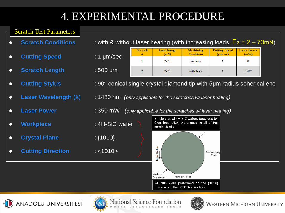
Scratch Conditions : with & without laser heating (with increasing loads, Fz = 2 – 70mN)
Cutting Speed : 1 μm/sec
Scratch Length : 500 μm
Cutting Stylus : 90° conical single crystal diamond tip with 5μm radius spherical end
Laser Wavelength (λ) : 1480 nm (only applicable for the scratches w/ laser heating)
Laser Power : 350 mW (only applicable for the scratches w/ laser heating)
Workpiece : 4H-SiC wafer
Crystal Plane : {1010}
Cutting Direction : <1010>
Scratch Test Parameters
4. EXPERIMENTAL PROCEDURE

Scratching resembles diamond turning machining Similarities in cutting mechanism (stress state)
Scratching is simpler than machining, sliding indentation(ductile scratch with small DoC)
Scratching is slow motion of ductile machining(m/s in machining vs. <1 mm /s in scratching)
4. EXPERIMENTAL PROCEDURE
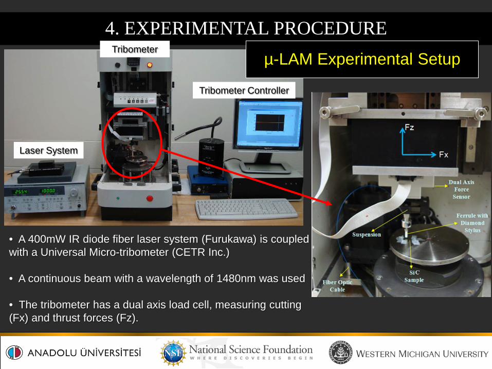
4. EXPERIMENTAL PROCEDURE
• A 400mW IR diode fiber laser system (Furukawa) is coupled with a Universal Micro-tribometer (CETR Inc.)
• A continuous beam with a wavelength of 1480nm was used
• The tribometer has a dual axis load cell, measuring cutting (Fx) and thrust forces (Fz).
Laser System
Tribometer
Tribometer Controller
µ-LAM Experimental Setup

4. EXPERIMENTAL PROCEDURE
The µ-LAM laser heating systemconsists of:
• diamond tip(transparent to that wavelength)
• a fiber-coupled IR diode laser(1480 laser Diode Module, Manufactured by Furukawa)
• a set of laser operation and control devices(LDC-3744B Laser Diode Controller, LDM-4980 Series Laser Diode Mount, ILX Light Wave Inc.)
@x40
Ferrule, 2mm diameter
Diamond tip

4. EXPERIMENTAL PROCEDURE
Diamond tip(5 µm radius)
Ferrule(2.5mm diameter)
(a) 5 µM RADIUS DIAMOND TIP ATTACHED ON THE END OF THE FERRULE USING UV-cured EPOXY
(b) CLOSE UP ON DIAMOND TIP EMBEDDED IN THE SOLIDIFIED EPOXY.
(b) (a)
Diamond Tip Attachment

5. RESULTS & DISCUSSIONS
In both images, it is evident that fracture occurs earlier (at a less load) forthe scratch performed with no leaser heating.
Micrographs showing brittle fracture of SiC along the scratch.

5. RESULTS & DISCUSSIONS
although both scratches are with the same load range, the extent of brittlefracture is much more severe for the scratch performed with no laser heating.
Micrograph showing scratches into brittle region at higher loads

5. RESULTS & DISCUSSIONS
The DBT of the scratch performed without laser heating is identified scratch performed with laser heating (left) exhibits a perfectly ductile behavior whereas
the scratch done without laser heating (right) indicates slight fracture (brittle behavior) ofthe material.
the scratch performed without laser heating is (apparently) deeper (210nm vs. 113nm) asit is difficult to control the DoC when the material removal mechanism is brittle
cross-section of the two scratches taken at an equal thrust force of approximately 35mN
DBT depth: 105nm
Cross-Sectional Evaluation**Cross sections were evaluated using a white light interferometer
(Surface roughness, depth and width of indents & scratches)

5. RESULTS & DISCUSSIONS
Cross-Sectional Evaluation
The DBT of the scratch performed with laser heating is identified At this load, the scratch performed with no laser heating shows signs of severe fracture The DBT depth of the scratch performed with laser heating was greater than the DBT
depth of the scratch performed without laser heating.
cross-section of the same two scratches (at a different point) taken at an equal thrust force of approx. 40mN
DBT depth: 240nm

5. RESULTS & DISCUSSIONS
Initial fracture occurrence No Laser : Fz = 35mN, Fx = 12mN (105nm depth) With Laser : Fz = 40mN, Fx = 14mN (240nm depth)
Force Data

Scratch Test Results comparing with & without laser heating
Machining Condition
Thrust Force
(Fz)
Cutting Force
(Fx)
Depth of Cut,(nm)
ScratchNature
No Laser 30mN 10mN 95nm DuctileWith Laser 30mN 10mN 145nm DuctileNo Laser 35mN 12mN* 105nm* DBT
With Laser 40mN 14mN* 240nm* DBT*Measurement taken just before the DBT occurs.
5. RESULTS & DISCUSSIONS

Scratch Test Results comparing with & without laser heating
5. RESULTS & DISCUSSIONS

µ-LAM scratch tests were successful in demonstrating theenhanced thermal softening of the material, resulting in a greaterDBT depth and an apparent increase in fracture toughness.
Laser heating was successfully demonstrated as evidenced by thesignificant increase in the ductile response of 4H-SiC in the{1010} plane along the <1010> direction.
Laser assisted (heating, thermal softening and reduced brittleness)material removal resulted in greater depths of cuts at less appliedthrust forces, smaller cutting forces and a larger critical DoC.
6. CONCLUSION
6. CONCLUSION
The enhanced ductile response is promising to increase thematerial removal rate in machining processes such as single pointdiamond turning.
Lesser tool wear is predicted due to the enhanced thermalsoftening of the material and lower cutting forces during thematerial removal process.
Better product quality (improved surface finish) and lessermachining time is anticipated due to the decrease in brittleresponse in the material.

5. ONGOING/FUTURE WORK
Medium power laser (Visotek Fiber Laser System,
976nm wavelength and 10W max. laser power) will
be coupled using optical components to a variety of
diamond tools seen below.
(multiple tool vendors are used such as Chardon Tool & Supply Inc., Ohio, USAand K&Y Diamond, Canada).
Various types of diamond tools will be
used in μ-LAM.
Mid-power Visotek laser system (976 nm, 10 W).

To further study the effects of high power laser heating on Si and SiC, an IPG fiber lasersystem (IPG Photonics Co., USA) (maximum power = 100W and wavelength, λ =1070nm) will be tested with a 1 mm nose radius diamond cutting tool.
High power IPG laser system (1070 nm, 100 W).
Diamond Tool X and Y
adjusments
Z adjustment
Laser mechanisms head with a beam delivery optics.
5. ONGOING/FUTURE WORK

Laser Head
UMT TribometerLaser Cable
and BDO
Diamond Cutting Tool
UMT Controller
IPG Laser system coupled with a laser beam delivery optics unit.
5. ONGOING/FUTURE WORK

Initial Results:
• The phase change in 4H-SiC was seen over a pressure range of 66 GPa• The phase change in 6H-SiC was seen over a pressure range of 88 GPaat 1500 - 1600 K (226 - 326 oC).
It is believed (from preliminary results) that all three polytypes appear to form adense cubic phase (3C) at these conditions. The data from these experiments isstill being analyzed to determine the characteristics of the newly formed highpressure phase, such as optical absorption over the wide range of wavelengths(UV through IR).
High pressure and temperature tests wereconducted at Argonne National Laboratory (ANL),Advanced Photon Source (APS) to determine thephase transition conditions and parameters of 4H,6H and 3C SiC.
5. ONGOING/FUTURE WORK

TEM of the cross-section of IR laser heated scratches on Si and SiC willhave been also performed to corroborate with the micro-Raman analysis.
The study will be extended to industrial end users and technologyproviders (such as TWS, MLPC and Adamant Kogyo Co. Ltd.) topursue applications of the technology, such as in virtual manufacturing(machining simulations) and manufacturing of advanced components(semiconductor, optical and structural ceramics).
Industries are interested in using the µ-LAM technology Electric Power Research Institute (EPRI)(using µ-LAM technology in the renewable energy generation especially in wind turbines) Adamant Kogyo Co. Ltd. (from Japan)(pursuing to develop manufacturing semiconductors based on µ-LAM technology)
5. ONGOING/FUTURE WORK

The effects of laser heating on the DBT µ-LAM of the following materials: Silicon Carbide (4H, 6H and 3C - SiC) Quartz (Fused Silica) Spinel (MgAl2O4)AlTiC Sapphire (synthetic) ZirconiaAlON
µ-LAM coupled with Single Point Diamond Turning (SPDT) Study the effect of laser heating/softening of material when combined with SPDT Evaluate fracture toughness and brittleness due to DBT as a result of thermal softening Improve surface finish of ceramics & semiconductors via ductile mode machining Minimize diamond tool wear as hardness of material is reduced
The novel µ-LAM prototype system can be used on precision machining of seminconductor and ceramicsto improve the machinability and enhance the overall manufacturing process.
Results obtained from this study are promising to further implement µ-LAM in operations such as SPDT.
5. ONGOING/FUTURE WORK

USA Department of Energy (DoE) National Science Foundation (NSF)[Grant#: CMMI-0757339]
Michigan Universities Commercialization Initiative (MUCI)
Adamant Kogyo Co. Ltd., Japan (Fiber Optic Components, LCDs, PrecisionProcessing Components, MEMS, Optical Fiber Current Sensors etc.)
Chardon Tool Co. , OHIO, USA
Argonne National Laboratory (ANL)
- Center for Nanoscale Materials (CNM)
- Advance Photon Source (APS)
ACKNOWLEDGEMENTS

Questions
thank you !

ADDITIONAL SLIDES


![µ ] µ o µ u d l ] v P Z © W l l µ ] µ o µ u l ] v P X µ ...](https://static.fdocuments.in/doc/165x107/6212ad0e8cd8cf34006f2a56/-o-u-d-l-v-p-z-w-l-l-o-.jpg)


![BKM INDUSTRIES LIMITED€¦ · 13. dZ }u vÇ] }v v }µ Z vÀ] }vu v v µ o]Ì v µ o }µ ]v µ ]v o ÁÇXt µ Ç}µ } µ Ç}µ u]o Á] ZÇ}µ } ] } ÇW ] v } v o µ } v Ç}µ Z vvµoZ](https://static.fdocuments.in/doc/165x107/5f7aa2ab21740547403de5fd/bkm-industries-limited-13-dz-u-v-v-v-z-v-vu-v-v-ooe-v-o-.jpg)


![CX Playbook (final) - actiac.org Playbook.pdf · ^ À ] µ µ µ µ ...](https://static.fdocuments.in/doc/165x107/5f9654b19de95b57da28eea5/cx-playbook-final-playbookpdf-.jpg)

