Dual J-K Flip-Flops With Preset And Clear datasheet
12
SN5476, SN54LS76A SN7476, SN74LS76A DUAL J-K FLIP-FLOPS WITH PRESET AND CLEAR SDLS121 – DECEMBER 1983 – REVISED MARCH 1988 1 POST OFFICE BOX 655303 • DALLAS, TEXAS 75265 Copyright 1988, Texas Instruments Incorporated PRODUCTION DATA information is current as of publication date. Products conform to specifications per the terms of Texas Instruments standard warranty. Production processing does not necessarily include testing of all parameters.
Transcript of Dual J-K Flip-Flops With Preset And Clear datasheet
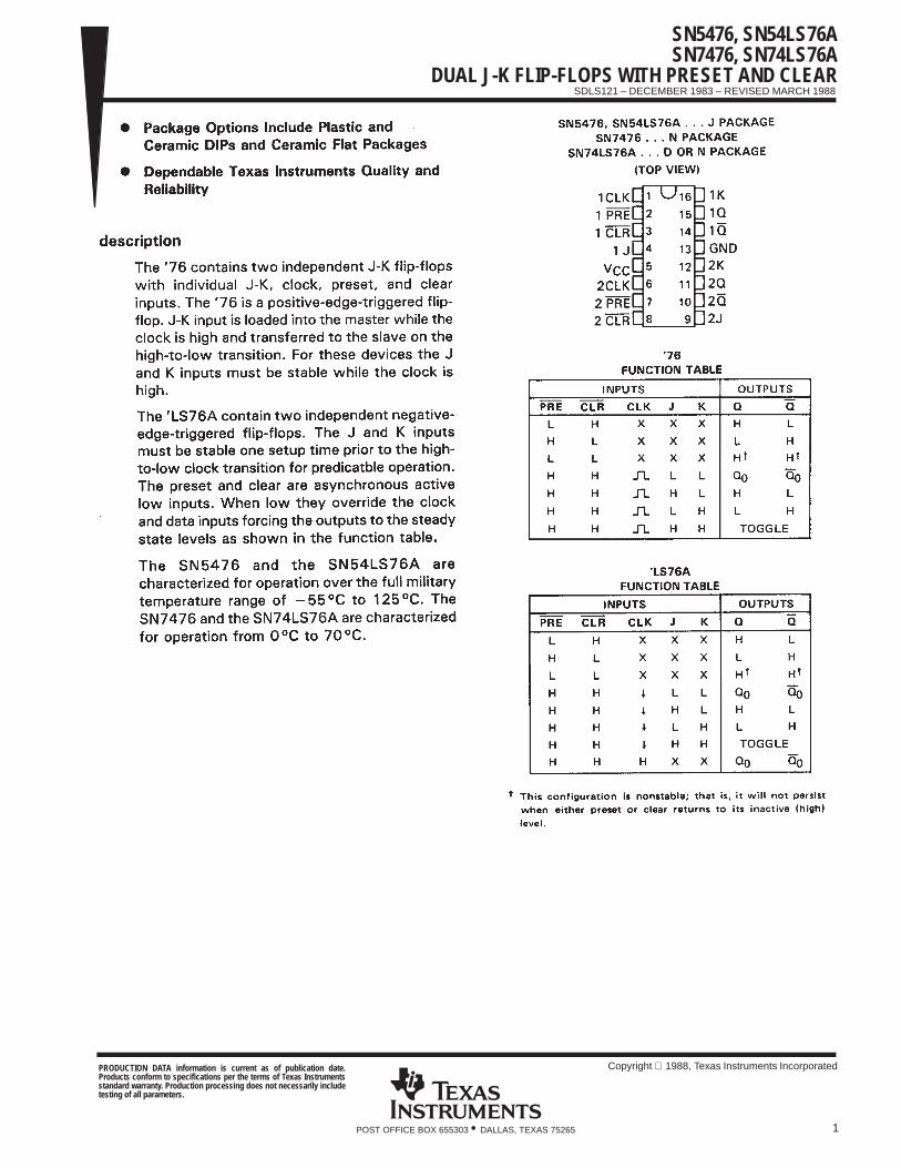
SN5476, SN54LS76ASN7476, SN74LS76A
DUAL J-K FLIP-FLOPS WITH PRESET AND CLEAR
SDLS121 – DECEMBER 1983 – REVISED MARCH 1988
1POST OFFICE BOX 655303 • DALLAS, TEXAS 75265
Copyright 1988, Texas Instruments IncorporatedPRODUCTION DATA information is current as of publication date.Products conform to specifications per the terms of Texas Instrumentsstandard warranty. Production processing does not necessarily includetesting of all parameters.

SN5476, SN54LS76ASN7476, SN74LS76ADUAL J-K FLIP-FLOPS WITH PRESET AND CLEAR
SDLS121 – DECEMBER 1983 – REVISED MARCH 1988
2 POST OFFICE BOX 655303 • DALLAS, TEXAS 75265

SN5476, SN54LS76ASN7476, SN74LS76A
DUAL J-K FLIP-FLOPS WITH PRESET AND CLEAR
SDLS121 – DECEMBER 1983 – REVISED MARCH 1988
3POST OFFICE BOX 655303 • DALLAS, TEXAS 75265

SN5476, SN54LS76ASN7476, SN74LS76ADUAL J-K FLIP-FLOPS WITH PRESET AND CLEAR
SDLS121 – DECEMBER 1983 – REVISED MARCH 1988
4 POST OFFICE BOX 655303 • DALLAS, TEXAS 75265

SN5476, SN54LS76ASN7476, SN74LS76A
DUAL J-K FLIP-FLOPS WITH PRESET AND CLEAR
SDLS121 – DECEMBER 1983 – REVISED MARCH 1988
5POST OFFICE BOX 655303 • DALLAS, TEXAS 75265

SN5476, SN54LS76ASN7476, SN74LS76ADUAL J-K FLIP-FLOPS WITH PRESET AND CLEAR
SDLS121 – DECEMBER 1983 – REVISED MARCH 1988
6 POST OFFICE BOX 655303 • DALLAS, TEXAS 75265

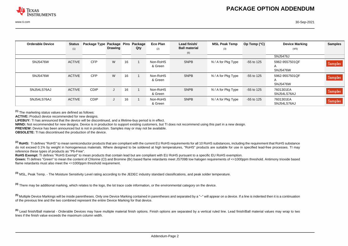
PACKAGE OPTION ADDENDUM
www.ti.com 30-Sep-2021
Addendum-Page 1
PACKAGING INFORMATION
Orderable Device Status(1)
Package Type PackageDrawing
Pins PackageQty
Eco Plan(2)
Lead finish/Ball material
(6)
MSL Peak Temp(3)
Op Temp (°C) Device Marking(4/5)
Samples
5962-9557501QEA ACTIVE CDIP J 16 1 Non-RoHS& Green
SNPB N / A for Pkg Type -55 to 125 5962-9557501QEASNJ5476J
5962-9557501QFA ACTIVE CFP W 16 1 Non-RoHS& Green
SNPB N / A for Pkg Type -55 to 125 5962-9557501QFASNJ5476W
5962-9557501QFA ACTIVE CFP W 16 1 Non-RoHS& Green
SNPB N / A for Pkg Type -55 to 125 5962-9557501QFASNJ5476W
7601301EA ACTIVE CDIP J 16 1 Non-RoHS& Green
SNPB N / A for Pkg Type -55 to 125 7601301EASNJ54LS76AJ
7601301EA ACTIVE CDIP J 16 1 Non-RoHS& Green
SNPB N / A for Pkg Type -55 to 125 7601301EASNJ54LS76AJ
JM38510/00204BEA ACTIVE CDIP J 16 1 Non-RoHS& Green
SNPB N / A for Pkg Type -55 to 125 JM38510/00204BEA
JM38510/00204BEA ACTIVE CDIP J 16 1 Non-RoHS& Green
SNPB N / A for Pkg Type -55 to 125 JM38510/00204BEA
M38510/00204BEA ACTIVE CDIP J 16 1 Non-RoHS& Green
SNPB N / A for Pkg Type -55 to 125 JM38510/00204BEA
M38510/00204BEA ACTIVE CDIP J 16 1 Non-RoHS& Green
SNPB N / A for Pkg Type -55 to 125 JM38510/00204BEA
SN5476J ACTIVE CDIP J 16 1 Non-RoHS& Green
SNPB N / A for Pkg Type -55 to 125 SN5476J
SN5476J ACTIVE CDIP J 16 1 Non-RoHS& Green
SNPB N / A for Pkg Type -55 to 125 SN5476J
SN54LS76AJ ACTIVE CDIP J 16 1 Non-RoHS& Green
SNPB N / A for Pkg Type -55 to 125 SN54LS76AJ
SN54LS76AJ ACTIVE CDIP J 16 1 Non-RoHS& Green
SNPB N / A for Pkg Type -55 to 125 SN54LS76AJ
SNJ5476J ACTIVE CDIP J 16 1 Non-RoHS& Green
SNPB N / A for Pkg Type -55 to 125 5962-9557501QEASNJ5476J
SNJ5476J ACTIVE CDIP J 16 1 Non-RoHS& Green
SNPB N / A for Pkg Type -55 to 125 5962-9557501QEA
PACKAGE OPTION ADDENDUM
www.ti.com 30-Sep-2021
Addendum-Page 2
Orderable Device Status(1)
Package Type PackageDrawing
Pins PackageQty
Eco Plan(2)
Lead finish/Ball material
(6)
MSL Peak Temp(3)
Op Temp (°C) Device Marking(4/5)
Samples
SNJ5476J
SNJ5476W ACTIVE CFP W 16 1 Non-RoHS& Green
SNPB N / A for Pkg Type -55 to 125 5962-9557501QFASNJ5476W
SNJ5476W ACTIVE CFP W 16 1 Non-RoHS& Green
SNPB N / A for Pkg Type -55 to 125 5962-9557501QFASNJ5476W
SNJ54LS76AJ ACTIVE CDIP J 16 1 Non-RoHS& Green
SNPB N / A for Pkg Type -55 to 125 7601301EASNJ54LS76AJ
SNJ54LS76AJ ACTIVE CDIP J 16 1 Non-RoHS& Green
SNPB N / A for Pkg Type -55 to 125 7601301EASNJ54LS76AJ
(1) The marketing status values are defined as follows:ACTIVE: Product device recommended for new designs.LIFEBUY: TI has announced that the device will be discontinued, and a lifetime-buy period is in effect.NRND: Not recommended for new designs. Device is in production to support existing customers, but TI does not recommend using this part in a new design.PREVIEW: Device has been announced but is not in production. Samples may or may not be available.OBSOLETE: TI has discontinued the production of the device.
(2) RoHS: TI defines "RoHS" to mean semiconductor products that are compliant with the current EU RoHS requirements for all 10 RoHS substances, including the requirement that RoHS substancedo not exceed 0.1% by weight in homogeneous materials. Where designed to be soldered at high temperatures, "RoHS" products are suitable for use in specified lead-free processes. TI mayreference these types of products as "Pb-Free".RoHS Exempt: TI defines "RoHS Exempt" to mean products that contain lead but are compliant with EU RoHS pursuant to a specific EU RoHS exemption.Green: TI defines "Green" to mean the content of Chlorine (Cl) and Bromine (Br) based flame retardants meet JS709B low halogen requirements of <=1000ppm threshold. Antimony trioxide basedflame retardants must also meet the <=1000ppm threshold requirement.
(3) MSL, Peak Temp. - The Moisture Sensitivity Level rating according to the JEDEC industry standard classifications, and peak solder temperature.
(4) There may be additional marking, which relates to the logo, the lot trace code information, or the environmental category on the device.
(5) Multiple Device Markings will be inside parentheses. Only one Device Marking contained in parentheses and separated by a "~" will appear on a device. If a line is indented then it is a continuationof the previous line and the two combined represent the entire Device Marking for that device.
(6) Lead finish/Ball material - Orderable Devices may have multiple material finish options. Finish options are separated by a vertical ruled line. Lead finish/Ball material values may wrap to twolines if the finish value exceeds the maximum column width.

PACKAGE OPTION ADDENDUM
www.ti.com 30-Sep-2021
Addendum-Page 3
Important Information and Disclaimer:The information provided on this page represents TI's knowledge and belief as of the date that it is provided. TI bases its knowledge and belief on informationprovided by third parties, and makes no representation or warranty as to the accuracy of such information. Efforts are underway to better integrate information from third parties. TI has taken andcontinues to take reasonable steps to provide representative and accurate information but may not have conducted destructive testing or chemical analysis on incoming materials and chemicals.TI and TI suppliers consider certain information to be proprietary, and thus CAS numbers and other limited information may not be available for release.
In no event shall TI's liability arising out of such information exceed the total purchase price of the TI part(s) at issue in this document sold by TI to Customer on an annual basis.


IMPORTANT NOTICE AND DISCLAIMERTI PROVIDES TECHNICAL AND RELIABILITY DATA (INCLUDING DATASHEETS), DESIGN RESOURCES (INCLUDING REFERENCEDESIGNS), APPLICATION OR OTHER DESIGN ADVICE, WEB TOOLS, SAFETY INFORMATION, AND OTHER RESOURCES “AS IS”AND WITH ALL FAULTS, AND DISCLAIMS ALL WARRANTIES, EXPRESS AND IMPLIED, INCLUDING WITHOUT LIMITATION ANYIMPLIED WARRANTIES OF MERCHANTABILITY, FITNESS FOR A PARTICULAR PURPOSE OR NON-INFRINGEMENT OF THIRDPARTY INTELLECTUAL PROPERTY RIGHTS.These resources are intended for skilled developers designing with TI products. You are solely responsible for (1) selecting the appropriateTI products for your application, (2) designing, validating and testing your application, and (3) ensuring your application meets applicablestandards, and any other safety, security, or other requirements. These resources are subject to change without notice. TI grants youpermission to use these resources only for development of an application that uses the TI products described in the resource. Otherreproduction and display of these resources is prohibited. No license is granted to any other TI intellectual property right or to any third partyintellectual property right. TI disclaims responsibility for, and you will fully indemnify TI and its representatives against, any claims, damages,costs, losses, and liabilities arising out of your use of these resources.TI’s products are provided subject to TI’s Terms of Sale (https:www.ti.com/legal/termsofsale.html) or other applicable terms available eitheron ti.com or provided in conjunction with such TI products. TI’s provision of these resources does not expand or otherwise alter TI’sapplicable warranties or warranty disclaimers for TI products.IMPORTANT NOTICE
Mailing Address: Texas Instruments, Post Office Box 655303, Dallas, Texas 75265Copyright © 2021, Texas Instruments Incorporated