
DUAL CHANNEL, 14-BIT,125/105/80/65 MSPS ADC WITH … · 1features applications description ads6245,...
76
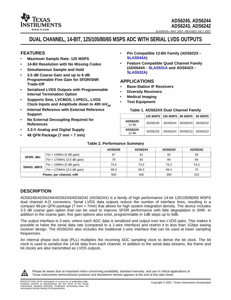
1FEATURES APPLICATIONS DESCRIPTION ADS6245, ADS6244 ADS6243, ADS6242 SLAS542A–MAY 2007–REVISED JULY 2007 www.ti.com DUAL CHANNEL, 14-BIT, 125/105/80/65 MSPS ADC WITH SERIAL LVDS OUTPUTS • Pin Compatible 12-Bit Family (ADS622X - SLAS543A) • Maximum Sample Rate: 125 MSPS • Feature Compatible Quad Channel Family • 14-Bit Resolution with No Missing Codes (ADS644X - SLAS531A and ADS642X - • Simultaneous Sample and Hold SLAS532A) • 3.5 dB Coarse Gain and up to 6 dB Programmable Fine Gain for SFDR/SNR Trade-Off • Base-Station IF Receivers • Serialized LVDS Outputs with Programmable • Diversity Receivers Internal Termination Option • Medical Imaging • Supports Sine, LVCMOS, LVPECL, LVDS • Test Equipment Clock Inputs and Amplitude down to 400 mV pp • Internal Reference with External Reference Table 1. ADS62XX Dual Channel Family Support 125 MSPS 105 MSPS 80 MSPS 65 MSPS • No External Decoupling Required for ADS624X ADS6245 ADS6244 ADS6243 ADS6242 References 14 Bit ADS622X • 3.3-V Analog and Digital Supply ADS6225 ADS6224 ADS6223 ADS6222 12 Bit • 48 QFN Package (7 mm × 7 mm) Table 2. Performance Summary ADS6245 ADS6244 ADS6243 ADS6242 Fin = 10MHz (0 dB gain) 87 91 92 93 SFDR, dBc Fin = 170MHz (3.5 dB gain) 79 83 84 84 Fin = 10MHz (0 dB gain) 73.4 73.4 74.2 74.3 SINAD, dBFS Fin = 170MHz (3.5 dB gain) 68.3 69.3 69.4 70 Power, per channel, mW 500 405 350 315 ADS6245/ADS6244/ADS6243/ADS6242 (ADS624X) is a family of high performance 14-bit 125/105/80/65 MSPS dual channel A-D converters. Serial LVDS data outputs reduce the number of interface lines, resulting in a compact 48-pin QFN package (7 mm × 7mm) that allows for high system integration density. The device includes 3.5 dB coarse gain option that can be used to improve SFDR performance with little degradation in SNR. In addition to the coarse gain, fine gain options also exist, programmable in 1dB steps up to 6dB. The output interface is 2-wire, where each ADC data is serialized and output over two LVDS pairs. This makes it possible to halve the serial data rate (compared to a 1-wire interface) and restrict it to less than 1Gbps easing receiver design. The ADS624X also includes the traditional 1-wire interface that can be used at lower sampling frequencies. An internal phase lock loop (PLL) multiplies the incoming ADC sampling clock to derive the bit clock. The bit clock is used to serialize the 14-bit data from each channel. In addition to the serial data streams, the frame and bit clocks are also transmitted as LVDS outputs. 1 Please be aware that an important notice concerning availability, standard warranty, and use in critical applications of Texas Instruments semiconductor products and disclaimers thereto appears at the end of this data sheet. PRODUCTION DATA information is current as of publication date. Copyright © 2007, Texas Instruments Incorporated Products conform to specifications per the terms of the Texas Instruments standard warranty. Production processing does not necessarily include testing of all parameters.
Transcript of DUAL CHANNEL, 14-BIT,125/105/80/65 MSPS ADC WITH … · 1features applications description ads6245,...
1FEATURES
APPLICATIONS
DESCRIPTION
ADS6245, ADS6244ADS6243, ADS6242
SLAS542A–MAY 2007–REVISED JULY 2007www.ti.com
DUAL CHANNEL, 14-BIT, 125/105/80/65 MSPS ADC WITH SERIAL LVDS OUTPUTS
• Pin Compatible 12-Bit Family (ADS622X -SLAS543A)• Maximum Sample Rate: 125 MSPS
• Feature Compatible Quad Channel Family• 14-Bit Resolution with No Missing Codes(ADS644X - SLAS531A and ADS642X -• Simultaneous Sample and HoldSLAS532A)
• 3.5 dB Coarse Gain and up to 6 dBProgrammable Fine Gain for SFDR/SNRTrade-Off • Base-Station IF Receivers
• Serialized LVDS Outputs with Programmable • Diversity ReceiversInternal Termination Option
• Medical Imaging• Supports Sine, LVCMOS, LVPECL, LVDS • Test Equipment
Clock Inputs and Amplitude down to 400 mVpp
• Internal Reference with External Reference Table 1. ADS62XX Dual Channel FamilySupport
125 MSPS 105 MSPS 80 MSPS 65 MSPS• No External Decoupling Required for ADS624X ADS6245 ADS6244 ADS6243 ADS6242References 14 Bit
ADS622X• 3.3-V Analog and Digital Supply ADS6225 ADS6224 ADS6223 ADS622212 Bit• 48 QFN Package (7 mm × 7 mm)
Table 2. Performance Summary
ADS6245 ADS6244 ADS6243 ADS6242
Fin = 10MHz (0 dB gain) 87 91 92 93SFDR, dBc
Fin = 170MHz (3.5 dB gain) 79 83 84 84
Fin = 10MHz (0 dB gain) 73.4 73.4 74.2 74.3SINAD, dBFS
Fin = 170MHz (3.5 dB gain) 68.3 69.3 69.4 70
Power, per channel, mW 500 405 350 315
ADS6245/ADS6244/ADS6243/ADS6242 (ADS624X) is a family of high performance 14-bit 125/105/80/65 MSPSdual channel A-D converters. Serial LVDS data outputs reduce the number of interface lines, resulting in acompact 48-pin QFN package (7 mm × 7mm) that allows for high system integration density. The device includes3.5 dB coarse gain option that can be used to improve SFDR performance with little degradation in SNR. Inaddition to the coarse gain, fine gain options also exist, programmable in 1dB steps up to 6dB.
The output interface is 2-wire, where each ADC data is serialized and output over two LVDS pairs. This makes itpossible to halve the serial data rate (compared to a 1-wire interface) and restrict it to less than 1Gbps easingreceiver design. The ADS624X also includes the traditional 1-wire interface that can be used at lower samplingfrequencies.
An internal phase lock loop (PLL) multiplies the incoming ADC sampling clock to derive the bit clock. The bitclock is used to serialize the 14-bit data from each channel. In addition to the serial data streams, the frame andbit clocks are also transmitted as LVDS outputs.
1
Please be aware that an important notice concerning availability, standard warranty, and use in critical applications ofTexas Instruments semiconductor products and disclaimers thereto appears at the end of this data sheet.
PRODUCTION DATA information is current as of publication date. Copyright © 2007, Texas Instruments IncorporatedProducts conform to specifications per the terms of the TexasInstruments standard warranty. Production processing does notnecessarily include testing of all parameters.
www.ti.com
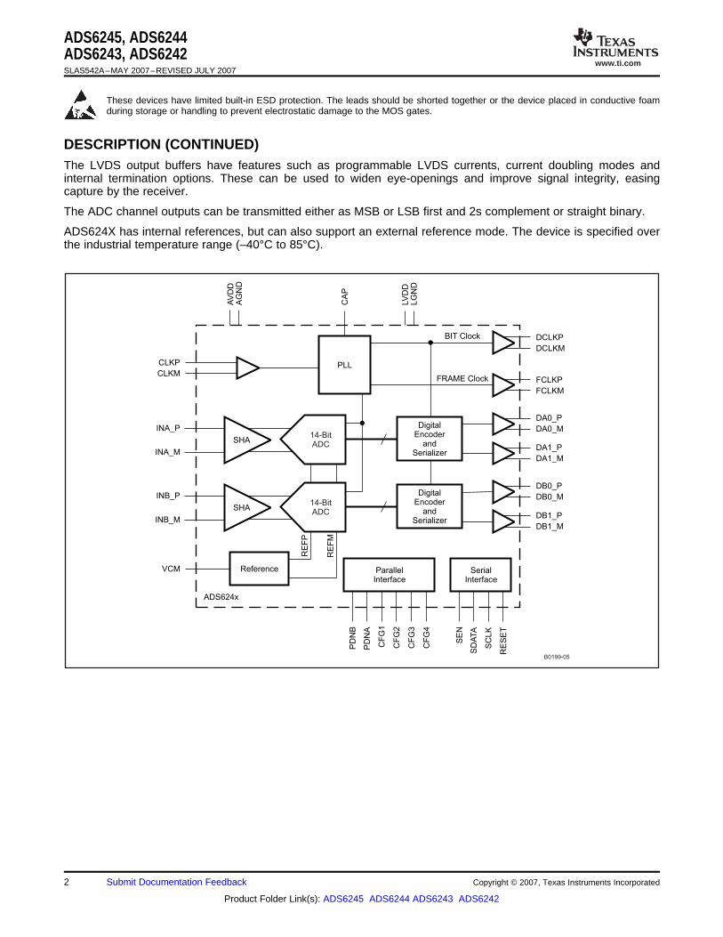
DESCRIPTION (CONTINUED)
Reference
INA_P
INA_M
CLKP
CLKM
VCM
SE
N
PD
NB
SD
ATA
PD
NA
SC
LK
CF
G1
RE
SE
T
CF
G2
CF
G3
CF
G4
DCLKP
DCLKM
ADS624x
SHA
FCLKP
FCLKM
INB_P
INB_M
SHA
RE
FP
RE
FM
PLL
BIT Clock
FRAME Clock
DA0_P
DA1_P
DA0_M
DA1_M
DB0_P
DB1_P
DB0_M
DB1_M
AV
DD
AG
ND
LV
DD
CA
P
LG
ND
SerialInterface
ParallelInterface
14-BitADC
14-BitADC
DigitalEncoder
andSerializer
DigitalEncoder
andSerializer
B0199-05
ADS6245, ADS6244ADS6243, ADS6242SLAS542A–MAY 2007–REVISED JULY 2007
These devices have limited built-in ESD protection. The leads should be shorted together or the device placed in conductive foamduring storage or handling to prevent electrostatic damage to the MOS gates.
The LVDS output buffers have features such as programmable LVDS currents, current doubling modes andinternal termination options. These can be used to widen eye-openings and improve signal integrity, easingcapture by the receiver.
The ADC channel outputs can be transmitted either as MSB or LSB first and 2s complement or straight binary.
ADS624X has internal references, but can also support an external reference mode. The device is specified overthe industrial temperature range (–40°C to 85°C).
2 Submit Documentation Feedback Copyright © 2007, Texas Instruments Incorporated
Product Folder Link(s): ADS6245 ADS6244 ADS6243 ADS6242
www.ti.com
ABSOLUTE MAXIMUM RATINGS (1)
ADS6245, ADS6244ADS6243, ADS6242
SLAS542A–MAY 2007–REVISED JULY 2007
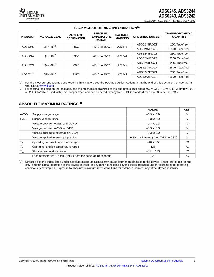
PACKAGE/ORDERING INFORMATION (1)
SPECIFIED TRANSPORT MEDIA,PACKAGE PACKAGEPRODUCT PACKAGE-LEAD TEMPERATURE ORDERING NUMBER QUANTITYDESIGNATOR MARKINGRANGE
ADS6245IRGZT 250, Tape/reelADS6245 QFN-48 (2) RGZ –40°C to 85°C AZ6245
ADS6245IRGZR 2500, Tape/reel
ADS6244IRGZT 250, Tape/reelADS6244 QFN-48 (2) RGZ –40°C to 85°C AZ6244
ADS6244IRGZR 2500, Tape/reel
ADS6243IRGZT 250, Tape/reelADS6243 QFN-48 (2) RGZ –40°C to 85°C AZ6243
ADS6243IRGZR 2500, Tape/reel
ADS6242IRGZT 250, Tape/reelADS6242 QFN-48 (2) RGZ –40°C to 85°C AZ6242
ADS6242IRGZR 2500, Tape/reel
(1) For the most current package and ordering information, see the Package Option Addendum at the end of this document, or see the TIweb site at www.ti.com.
(2) For thermal pad size on the package, see the mechanical drawings at the end of this data sheet. θJA = 23.17 °C/W (0 LFM air flow), θJC= 22.1 °C/W when used with 2 oz. copper trace and pad soldered directly to a JEDEC standard four layer 3 in. x 3 in. PCB.
VALUE UNIT
AVDD Supply voltage range –0.3 to 3.9 V
LVDD Supply voltage range –0.3 to 3.9 V
Voltage between AGND and DGND –0.3 to 0.3 V
Voltage between AVDD to LVDD –0.3 to 3.3 V
Voltage applied to external pin, VCM –0.3 to 2.0 V
Voltage applied to analog input pins –0.3V to minimum ( 3.6, AVDD + 0.3V) V
TA Operating free-air temperature range –40 to 85 °C
TJ Operating junction temperature range 125 °C
Tstg Storage temperature range –65 to 150 °C
Lead temperature 1,6 mm (1/16") from the case for 10 seconds 220 °C
(1) Stresses beyond those listed under absolute maximum ratings may cause permanent damage to the device. These are stress ratingsonly, and functional operation of the device at these or any other conditions beyond those indicated under recommended operatingconditions is not implied. Exposure to absolute-maximum-rated conditions for extended periods may affect device reliability.
Copyright © 2007, Texas Instruments Incorporated Submit Documentation Feedback 3
Product Folder Link(s): ADS6245 ADS6244 ADS6243 ADS6242
www.ti.com
RECOMMENDED OPERATING CONDITIONS
ELECTRICAL CHARACTERISTICS
ADS6245, ADS6244ADS6243, ADS6242SLAS542A–MAY 2007–REVISED JULY 2007
over operating free-air temperature range (unless otherwise noted)
MIN NOM MAX UNIT
SUPPLIES
AVDD Analog supply voltage 3.0 3.3 3.6 V
LVDD LVDS Buffer supply voltage 3.0 3.3 3.6 V
ANALOG INPUTS
Differential input voltage range 2 Vpp
1.5Input common-mode voltage V±0.1
Voltage applied on VCM in external reference mode 1.45 1.50 1.55 V
CLOCK INPUT
ADS6245 5 125
ADS6244 5 105Input clock sample rate, Fs MSPS
ADS6243 5 80
ADS6242 5 65
Sine wave, ac-coupled 0.4 1.5
LVPECL, ac-coupled ± 0.8Input clock amplitude differential (VCLKP – VCLKM) Vpp
LVDS, ac-coupled ± 0.35
LVCMOS, ac-coupled 3.3
Input Clock duty cycle 35% 50% 65%
DIGITAL OUTPUTS
Without internal termination 5Maximum external load capacitance from eachCLOAD pFoutput pin to DGND With internal termination 10
RLOAD Differential load resistance (external) between the LVDS output pairs 100 ΩTA Operating free-air temperature –40 85 °C
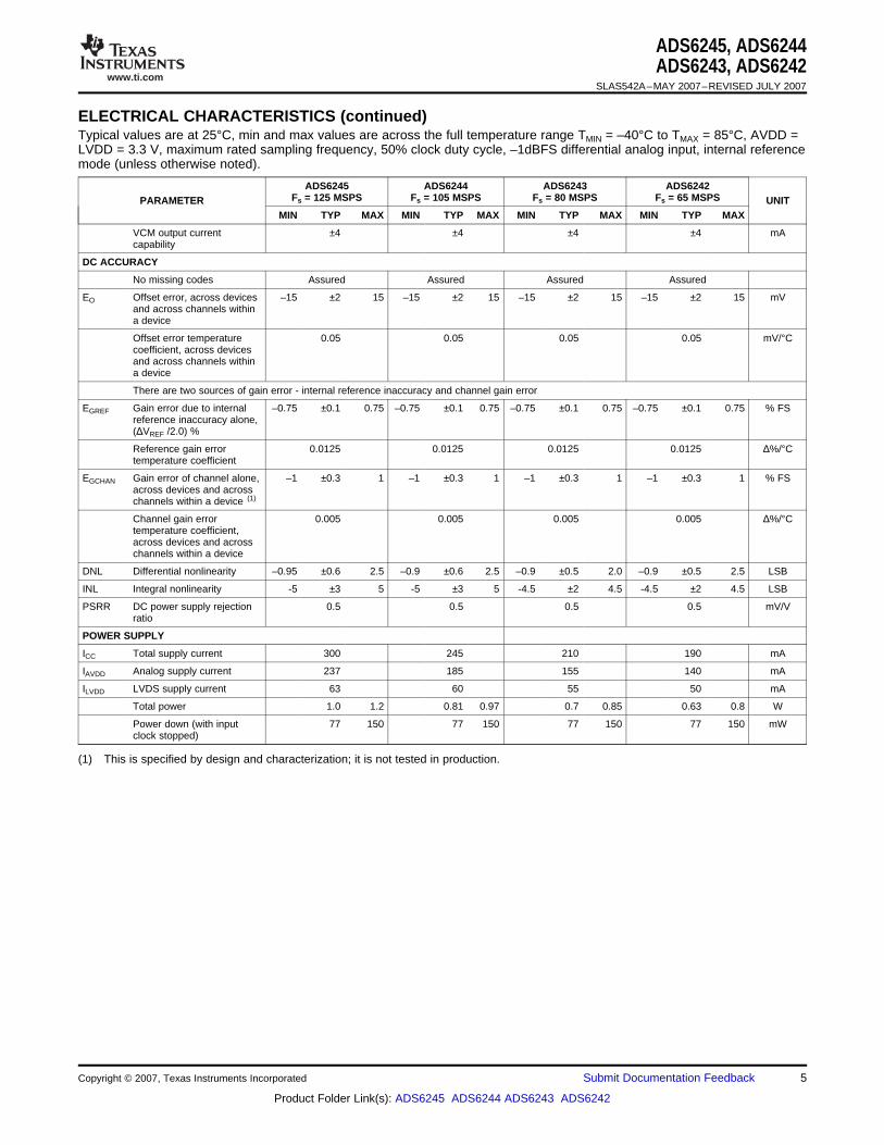
Typical values are at 25°C, min and max values are across the full temperature range TMIN = –40°C to TMAX = 85°C, AVDD =LVDD = 3.3 V, maximum rated sampling frequency, 50% clock duty cycle, –1dBFS differential analog input, internal referencemode (unless otherwise noted).
ADS6245 ADS6244 ADS6243 ADS6242Fs = 125 MSPS Fs = 105 MSPS Fs = 80 MSPS Fs = 65 MSPSPARAMETER UNIT
MIN TYP MAX MIN TYP MAX MIN TYP MAX MIN TYP MAX
RESOLUTION 14 14 14 14 Bits
ANALOG INPUT
Differential input voltage 2.0 2.0 2.0 2.0 VPPrange
Differential input 7 7 7 7 pFcapacitance
Analog input bandwidth 500 500 500 500 MHz
Analog input common mode 155 130 100 81 μAcurrent (per input pin ofeach ADC)
REFERENCE VOLTAGES
VREFB Internal reference bottom 1.0 1.0 1.0 1.0 Vvoltage
VREFT Internal reference top 2.0 2.0 2.0 2.0 Vvoltage
ΔVREF Internal reference error, –15 ±2 15 –15 ±2 15 –15 ±2 15 –15 ±2 15 mV(VREFT–VREFB)
VCM Common mode output 1.5 1.5 1.5 1.5 Vvoltage
4 Submit Documentation Feedback Copyright © 2007, Texas Instruments Incorporated
Product Folder Link(s): ADS6245 ADS6244 ADS6243 ADS6242
www.ti.com
ADS6245, ADS6244ADS6243, ADS6242
SLAS542A–MAY 2007–REVISED JULY 2007
ELECTRICAL CHARACTERISTICS (continued)Typical values are at 25°C, min and max values are across the full temperature range TMIN = –40°C to TMAX = 85°C, AVDD =LVDD = 3.3 V, maximum rated sampling frequency, 50% clock duty cycle, –1dBFS differential analog input, internal referencemode (unless otherwise noted).
ADS6245 ADS6244 ADS6243 ADS6242Fs = 125 MSPS Fs = 105 MSPS Fs = 80 MSPS Fs = 65 MSPSPARAMETER UNIT
MIN TYP MAX MIN TYP MAX MIN TYP MAX MIN TYP MAX
VCM output current ±4 ±4 ±4 ±4 mAcapability
DC ACCURACY
No missing codes Assured Assured Assured Assured
EO Offset error, across devices –15 ±2 15 –15 ±2 15 –15 ±2 15 –15 ±2 15 mVand across channels withina device
Offset error temperature 0.05 0.05 0.05 0.05 mV/°Ccoefficient, across devicesand across channels withina device
There are two sources of gain error - internal reference inaccuracy and channel gain error
EGREF Gain error due to internal –0.75 ±0.1 0.75 –0.75 ±0.1 0.75 –0.75 ±0.1 0.75 –0.75 ±0.1 0.75 % FSreference inaccuracy alone,(ΔVREF /2.0) %
Reference gain error 0.0125 0.0125 0.0125 0.0125 Δ%/°Ctemperature coefficient
EGCHAN Gain error of channel alone, –1 ±0.3 1 –1 ±0.3 1 –1 ±0.3 1 –1 ±0.3 1 % FSacross devices and acrosschannels within a device (1)
Channel gain error 0.005 0.005 0.005 0.005 Δ%/°Ctemperature coefficient,across devices and acrosschannels within a device
DNL Differential nonlinearity –0.95 ±0.6 2.5 –0.9 ±0.6 2.5 –0.9 ±0.5 2.0 –0.9 ±0.5 2.5 LSB
INL Integral nonlinearity -5 ±3 5 -5 ±3 5 -4.5 ±2 4.5 -4.5 ±2 4.5 LSB
PSRR DC power supply rejection 0.5 0.5 0.5 0.5 mV/Vratio
POWER SUPPLY
ICC Total supply current 300 245 210 190 mA
IAVDD Analog supply current 237 185 155 140 mA
ILVDD LVDS supply current 63 60 55 50 mA
Total power 1.0 1.2 0.81 0.97 0.7 0.85 0.63 0.8 W
Power down (with input 77 150 77 150 77 150 77 150 mWclock stopped)
(1) This is specified by design and characterization; it is not tested in production.
Copyright © 2007, Texas Instruments Incorporated Submit Documentation Feedback 5
Product Folder Link(s): ADS6245 ADS6244 ADS6243 ADS6242
www.ti.com
ELECTRICAL CHARACTERISTICS
ADS6245, ADS6244ADS6243, ADS6242SLAS542A–MAY 2007–REVISED JULY 2007
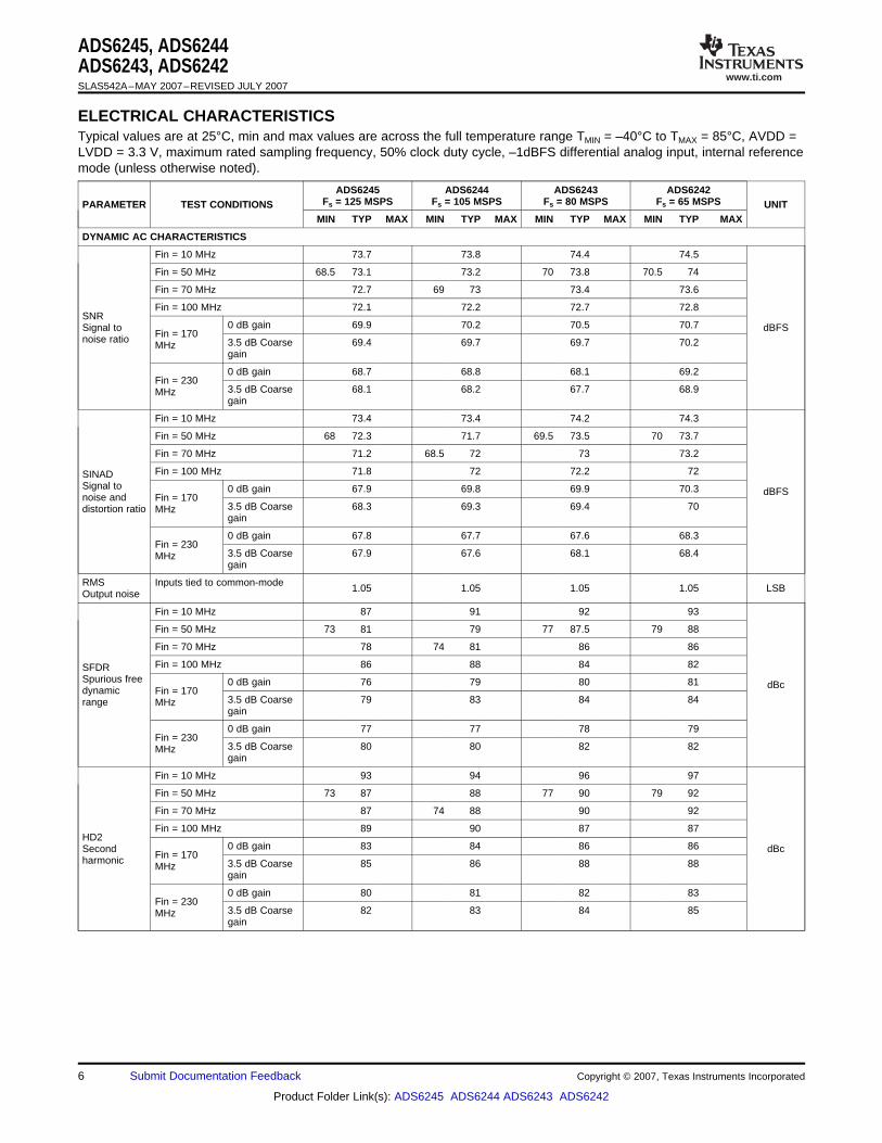
Typical values are at 25°C, min and max values are across the full temperature range TMIN = –40°C to TMAX = 85°C, AVDD =LVDD = 3.3 V, maximum rated sampling frequency, 50% clock duty cycle, –1dBFS differential analog input, internal referencemode (unless otherwise noted).
ADS6245 ADS6244 ADS6243 ADS6242Fs = 125 MSPS Fs = 105 MSPS Fs = 80 MSPS Fs = 65 MSPSPARAMETER TEST CONDITIONS UNIT
MIN TYP MAX MIN TYP MAX MIN TYP MAX MIN TYP MAX
DYNAMIC AC CHARACTERISTICS
Fin = 10 MHz 73.7 73.8 74.4 74.5
Fin = 50 MHz 68.5 73.1 73.2 70 73.8 70.5 74
Fin = 70 MHz 72.7 69 73 73.4 73.6
Fin = 100 MHz 72.1 72.2 72.7 72.8SNR
0 dB gain 69.9 70.2 70.5 70.7Signal to dBFSFin = 170noise ratio 3.5 dB Coarse 69.4 69.7 69.7 70.2MHz
gain
0 dB gain 68.7 68.8 68.1 69.2Fin = 230
3.5 dB Coarse 68.1 68.2 67.7 68.9MHzgain
Fin = 10 MHz 73.4 73.4 74.2 74.3
Fin = 50 MHz 68 72.3 71.7 69.5 73.5 70 73.7
Fin = 70 MHz 71.2 68.5 72 73 73.2
Fin = 100 MHz 71.8 72 72.2 72SINADSignal to 0 dB gain 67.9 69.8 69.9 70.3 dBFSnoise and Fin = 170
3.5 dB Coarse 68.3 69.3 69.4 70distortion ratio MHzgain
0 dB gain 67.8 67.7 67.6 68.3Fin = 230
3.5 dB Coarse 67.9 67.6 68.1 68.4MHzgain
RMS Inputs tied to common-mode 1.05 1.05 1.05 1.05 LSBOutput noise
Fin = 10 MHz 87 91 92 93
Fin = 50 MHz 73 81 79 77 87.5 79 88
Fin = 70 MHz 78 74 81 86 86
Fin = 100 MHz 86 88 84 82SFDRSpurious free 0 dB gain 76 79 80 81 dBcdynamic Fin = 170
3.5 dB Coarse 79 83 84 84range MHzgain
0 dB gain 77 77 78 79Fin = 230
3.5 dB Coarse 80 80 82 82MHzgain
Fin = 10 MHz 93 94 96 97
Fin = 50 MHz 73 87 88 77 90 79 92
Fin = 70 MHz 87 74 88 90 92
Fin = 100 MHz 89 90 87 87HD2
0 dB gain 83 84 86 86Second dBcFin = 170harmonic 3.5 dB Coarse 85 86 88 88MHz
gain
0 dB gain 80 81 82 83Fin = 230
3.5 dB Coarse 82 83 84 85MHzgain
6 Submit Documentation Feedback Copyright © 2007, Texas Instruments Incorporated
Product Folder Link(s): ADS6245 ADS6244 ADS6243 ADS6242
www.ti.com
ADS6245, ADS6244ADS6243, ADS6242
SLAS542A–MAY 2007–REVISED JULY 2007
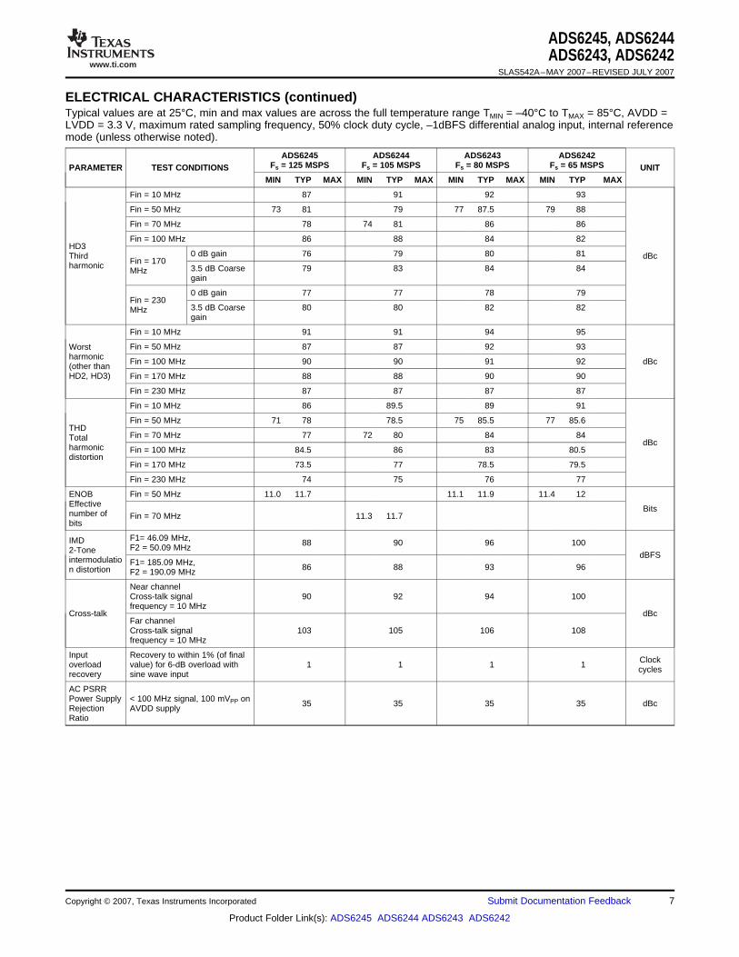
ELECTRICAL CHARACTERISTICS (continued)Typical values are at 25°C, min and max values are across the full temperature range TMIN = –40°C to TMAX = 85°C, AVDD =LVDD = 3.3 V, maximum rated sampling frequency, 50% clock duty cycle, –1dBFS differential analog input, internal referencemode (unless otherwise noted).
ADS6245 ADS6244 ADS6243 ADS6242Fs = 125 MSPS Fs = 105 MSPS Fs = 80 MSPS Fs = 65 MSPSPARAMETER TEST CONDITIONS UNIT
MIN TYP MAX MIN TYP MAX MIN TYP MAX MIN TYP MAX
Fin = 10 MHz 87 91 92 93
Fin = 50 MHz 73 81 79 77 87.5 79 88
Fin = 70 MHz 78 74 81 86 86
Fin = 100 MHz 86 88 84 82HD3
0 dB gain 76 79 80 81Third dBcFin = 170harmonic 3.5 dB Coarse 79 83 84 84MHz
gain
0 dB gain 77 77 78 79Fin = 230
3.5 dB Coarse 80 80 82 82MHzgain
Fin = 10 MHz 91 91 94 95
Fin = 50 MHz 87 87 92 93Worstharmonic Fin = 100 MHz 90 90 91 92 dBc(other thanHD2, HD3) Fin = 170 MHz 88 88 90 90
Fin = 230 MHz 87 87 87 87
Fin = 10 MHz 86 89.5 89 91
Fin = 50 MHz 71 78 78.5 75 85.5 77 85.6THD
Fin = 70 MHz 77 72 80 84 84Total dBcharmonic Fin = 100 MHz 84.5 86 83 80.5distortion
Fin = 170 MHz 73.5 77 78.5 79.5
Fin = 230 MHz 74 75 76 77
ENOB Fin = 50 MHz 11.0 11.7 11.1 11.9 11.4 12Effective Bitsnumber of Fin = 70 MHz 11.3 11.7bits
F1= 46.09 MHz,IMD 88 90 96 100F2 = 50.09 MHz2-Tone dBFSintermodulatio F1= 185.09 MHz, 86 88 93 96n distortion F2 = 190.09 MHz
Near channelCross-talk signal 90 92 94 100frequency = 10 MHz
Cross-talk dBcFar channelCross-talk signal 103 105 106 108frequency = 10 MHz
Input Recovery to within 1% (of final Clockoverload value) for 6-dB overload with 1 1 1 1 cyclesrecovery sine wave input
AC PSRRPower Supply < 100 MHz signal, 100 mVPP on 35 35 35 35 dBcRejection AVDD supplyRatio
Copyright © 2007, Texas Instruments Incorporated Submit Documentation Feedback 7
Product Folder Link(s): ADS6245 ADS6244 ADS6243 ADS6242
www.ti.com
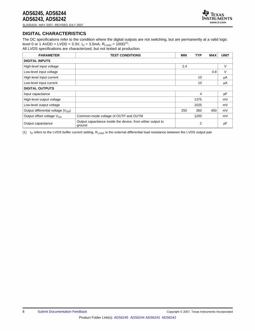
DIGITAL CHARACTERISTICS
ADS6245, ADS6244ADS6243, ADS6242SLAS542A–MAY 2007–REVISED JULY 2007
The DC specifications refer to the condition where the digital outputs are not switching, but are permanently at a valid logiclevel 0 or 1 AVDD = LVDD = 3.3V, IO = 3.5mA, RLOAD = 100Ω (1).All LVDS specifications are characterized, but not tested at production.
PARAMETER TEST CONDITIONS MIN TYP MAX UNIT
DIGITAL INPUTS
High-level input voltage 2.4 V
Low-level input voltage 0.8 V
High-level input current 10 μA
Low-level input current 10 μA
DIGITAL OUTPUTS
Input capacitance 4 pF
High-level output voltage 1375 mV
Low-level output voltage 1025 mV
Output differential voltage |VOD| 250 350 450 mV
Output offset voltage VOS Common-mode voltage of OUTP and OUTM 1200 mV
Output capacitance inside the device, from either output toOutput capacitance 2 pFground
(1) IO refers to the LVDS buffer current setting, RLOAD is the external differential load resistance between the LVDS output pair
8 Submit Documentation Feedback Copyright © 2007, Texas Instruments Incorporated
Product Folder Link(s): ADS6245 ADS6244 ADS6243 ADS6242
www.ti.com
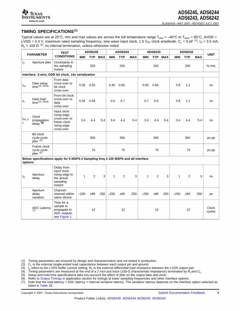
TIMING SPECIFICATIONS (1)
ADS6245, ADS6244ADS6243, ADS6242
SLAS542A–MAY 2007–REVISED JULY 2007
Typical values are at 25°C, min and max values are across the full temperature range TMIN = –40°C to TMAX = 85°C, AVDD =LVDD = 3.3 V, maximum rated sampling frequency, sine wave input clock, 1.5 VPP clock amplitude, CL = 5 pF (2), IO = 3.5 mA,RL = 100 Ω (3), no internal termination, unless otherwise noted.
ADS6245 ADS6244 ADS6243 ADS6242TESTPARAMETER UNITCONDITIONS MIN TYP MAX MIN TYP MAX MIN TYP MAX MIN TYP MAX
tJ Aperture jitter Uncertainty inthe sampling 250 250 250 250 fs rmsinstant
Interface: 2-wire, DDR bit clock, 14x serialization
From dataData setup cross-over totsu 0.35 0.55 0.45 0.65 0.65 0.85 0.8 1.1 nstime (4) (5) (6) bit clock
cross-over
From bit clockData hold cross-over toth 0.35 0.58 0.5 0.7 0.7 0.9 0.8 1.1 nstime (4) (5) (6) data
cross-over
Input clockrising edgeClocktpd_cl cross-over topropagation 3.4 4.4 5.4 3.4 4.4 5.4 3.4 4.4 5.4 3.4 4.4 5.4 ns
k frame clockdelay (6)rising edgecross-over
Bit clockcycle-cycle 350 350 350 350 ps ppjitter (5)
Frame clockcycle-cycle 75 75 75 75 ps ppjitter (5)
Below specifications apply for 5 MSPS ≤ Sampling freq ≤ 125 MSPS and all interfaceoptions
Delay frominput clock
Aperture rising edge totA 1 2 3 1 2 3 1 2 3 1 2 3 nsdelay the actualsamplinginstant
Aperture Channel-delay channel within –250 ±80 250 –250 ±80 250 –250 ±80 250 –250 ±80 250 psvariation same device
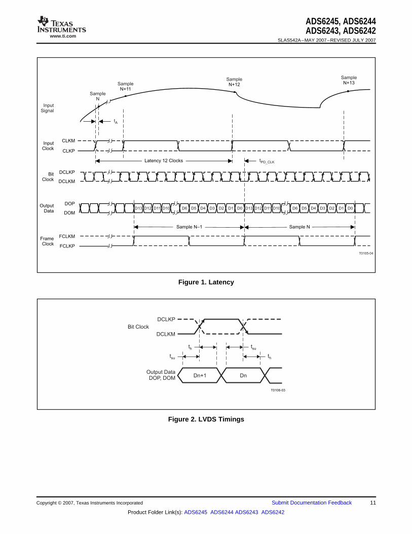
Time for asample toADC Latency Clockpropagate to 12 12 12 12(7) cyclesADC outputs,see Figure 1
(1) Timing parameters are ensured by design and characterization and not tested in production.(2) CL is the external single-ended load capacitance between each output pin and ground.(3) Io refers to the LVDS buffer current setting; RL is the external differential load resistance between the LVDS output pair.(4) Timing parameters are measured at the end of a 2 inch pcb trace (100-Ω characteristic impedance) terminated by RLand CL.(5) Setup and hold time specifications take into account the effect of jitter on the output data and clock.(6) Refer to Output Timings in application section for timings at lower sampling frequencies and other interface options.(7) Note that the total latency = ADC latency + internal serializer latency. The serializer latency depends on the interface option selected as
listed in Table 28.
Copyright © 2007, Texas Instruments Incorporated Submit Documentation Feedback 9
Product Folder Link(s): ADS6245 ADS6244 ADS6243 ADS6242
www.ti.com
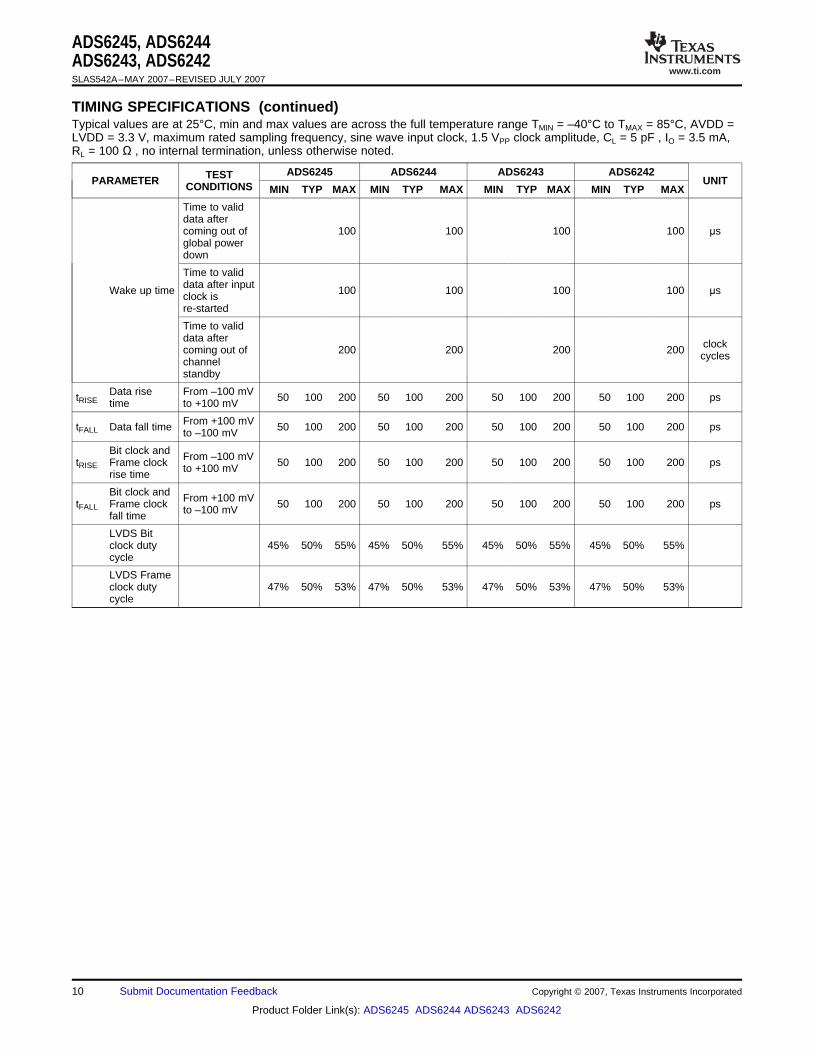
ADS6245, ADS6244ADS6243, ADS6242SLAS542A–MAY 2007–REVISED JULY 2007
TIMING SPECIFICATIONS (continued)Typical values are at 25°C, min and max values are across the full temperature range TMIN = –40°C to TMAX = 85°C, AVDD =LVDD = 3.3 V, maximum rated sampling frequency, sine wave input clock, 1.5 VPP clock amplitude, CL = 5 pF , IO = 3.5 mA,RL = 100 Ω , no internal termination, unless otherwise noted.
ADS6245 ADS6244 ADS6243 ADS6242TESTPARAMETER UNITCONDITIONS MIN TYP MAX MIN TYP MAX MIN TYP MAX MIN TYP MAX
Time to validdata aftercoming out of 100 100 100 100 μsglobal powerdown
Time to validdata after inputWake up time 100 100 100 100 μsclock isre-started
Time to validdata after clockcoming out of 200 200 200 200 cycleschannelstandby
Data rise From –100 mVtRISE 50 100 200 50 100 200 50 100 200 50 100 200 pstime to +100 mV
From +100 mVtFALL Data fall time 50 100 200 50 100 200 50 100 200 50 100 200 psto –100 mV
Bit clock and From –100 mVtRISE Frame clock 50 100 200 50 100 200 50 100 200 50 100 200 psto +100 mVrise time
Bit clock and From +100 mVtFALL Frame clock 50 100 200 50 100 200 50 100 200 50 100 200 psto –100 mVfall time
LVDS Bitclock duty 45% 50% 55% 45% 50% 55% 45% 50% 55% 45% 50% 55%cycle
LVDS Frameclock duty 47% 50% 53% 47% 50% 53% 47% 50% 53% 47% 50% 53%cycle
10 Submit Documentation Feedback Copyright © 2007, Texas Instruments Incorporated
Product Folder Link(s): ADS6245 ADS6244 ADS6243 ADS6242
www.ti.com
DCLKP
DCLKM
CLKM
CLKP
FCLKM
FCLKP
DOP
DOM
Sample N–1
tA
tPD_CLK
SampleN
SampleN+11
SampleN+12
SampleN+13
InputSignal
InputClock
BitClock
OutputData
FrameClock
D13 D13D3 D3D11 D11D5 D5D1 D1D12 D12D6 D6D2 D2D10 D10D4 D4D0 D0
Latency 12 Clocks
Sample N
T0105-04
T0106-03
Bit Clock
DCLKP
Output DataDOP, DOM
tsu th
th tsu
DCLKM
Dn+1 Dn
ADS6245, ADS6244ADS6243, ADS6242
SLAS542A–MAY 2007–REVISED JULY 2007
Figure 1. Latency
Figure 2. LVDS Timings
Copyright © 2007, Texas Instruments Incorporated Submit Documentation Feedback 11
Product Folder Link(s): ADS6245 ADS6244 ADS6243 ADS6242
www.ti.com
DEVICE PROGRAMMING MODES
USING PARALLEL INTERFACE CONTROL ONLY
USING SERIAL INTERFACE PROGRAMMING ONLY
USING BOTH THE SERIAL INTERFACE AND PARALLEL CONTROLS
ADS6245, ADS6244ADS6243, ADS6242SLAS542A–MAY 2007–REVISED JULY 2007
ADS624X offers flexibility with several programmable features that are easily configured.
The device can be configured independently using either parallel interface control or serial interfaceprogramming.
In addition, the device supports a third configuration mode, where both the parallel interface and the serial controlregisters are used. In this mode, the priority between the parallel and serial interfaces is determined by a prioritytable (Table 4). If this additional level of flexibility is not required, the user can select either the serial interfaceprogramming or the parallel interface control.
To control the device using parallel interface, keep RESET tied to high (LVDD). Pins CFG1, CFG2, CFG3,CFG4, PDNA, PDNB, SEN, SCLK, and SDATA are used to directly control certain functions of the ADC. Afterpower-up, the device will automatically get configured as per the parallel pin voltage settings (Table 5 to Table 9)and no reset is required. In this mode, SEN, SCLK, and SDATA function as parallel interface control pins.
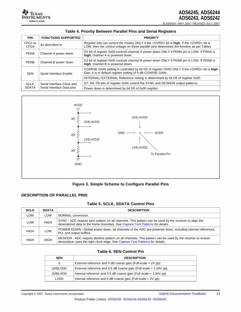
Frequently used functions are controlled in this mode—output data interface and format, power down modes,coarse gain and internal/external reference. The parallel pins can be configured using a simple resistor string asillustrated in Figure 3.
Table 3 has a description of the modes controlled by the parallel pins.
Table 3. Parallel Pin Definition
PIN CONTROL FUNCTIONS
SEN Coarse gain and internal/external reference.
SCLK, SDATA Sync, deskew patterns and global power down.
PDNA, PDNB Dedicated pins for individual channel power down
CFG1 1-wire/2-wire and DDR/SDR bit clock
CFG2 14x/16x serialization and SDR bit clock capture edge
CFG3 Reserved function. Tie CFG3 to Ground.
CFG4 MSB/LSB First and data format.
In this mode, SEN, SDATA, and SCLK function as serial interface pins and are used to access the internalregisters of ADC. The registers must first be reset to their default values either by applying a pulse on RESETpin or by a high setting on the <RST> bit (in register ). After reset, the RESET pin must be kept low.
The serial interface section describes the register programming and register reset in more detail.
Since the parallel pins (CFG1-4, PDNA and PDNB) are not used in this mode, they must be tied to ground. Theregister override bit <OVRD> - D10 in register 0x0D has to be set high to disable the control of parallel interfacepins in this serial interface control ONLY mode.
For increased flexibility, a combination of serial interface registers and parallel pin controls (CFG1-4, PDNA andPDNB) can also be used to configure the device.
The parallel interface control pins CFG1 to CFG4 and PDNA, PDNB are available. After power-up, the device willautomatically get configured as per the parallel pin voltage settings (Table 5 to Table 12) and no reset isrequired. A simple resistor string can be used as illustrated in Figure 3.
SEN, SDATA, and SCLK function as serial interface pins and are used to access the internal registers of ADC.The registers must first be reset to their default values either by applying a pulse on RESET pin or by a highsetting on the <RST> bit (in register ). After reset, the RESET pin must be kept low.
The serial interface section describes the register programming and register reset in more detail.
Since some functions are controlled using both the parallel pins and serial registers, the priority between the twois determined by a priority table (Table 4).
12 Submit Documentation Feedback Copyright © 2007, Texas Instruments Incorporated
Product Folder Link(s): ADS6245 ADS6244 ADS6243 ADS6242
www.ti.com
(3/8) AVDD
(3/8) AVDD
To Parallel Pin3R
AVDD
AVDDGND
GND
3R
2R
(5/8) AVDD
(5/8) AVDD
DESCRIPTION OF PARALLEL PINS
ADS6245, ADS6244ADS6243, ADS6242
SLAS542A–MAY 2007–REVISED JULY 2007
Table 4. Priority Between Parallel Pins and Serial Registers
PIN FUNCTIONS SUPPORTED PRIORITY
CFG1 to Register bits can control the modes ONLY if the <OVRD> bit is high. If the <OVRD> bit isAs described inCFG4 LOW, then the control voltage on these parallel pins determines the function as per Tables
D2 bit of register 0x00 controls channel A power down ONLY if PDNA pin is LOW. If PDNA isPDNA Channel A power down high, channel A is powered down.
D3 bit of register 0x00 controls channel B power down ONLY if PDNB pin is LOW. If PDNB isPDNB Channel B power down high, channel B is powered down.
COARSE GAIN setting is controlled by bit D5 of register 0X0D ONLY if the <OVRD> bit is high.Else, it is in default register setting of 0 dB COARSE GAIN.SEN Serial Interface EnableINTERNAL/ EXTERNAL Reference setting is determined by bit D6 of register 0x00.
D7, D6, D5 bits of register 0x0A control the SYNC and DESKEW output patterns.SCLK, Serial Interface Clock andSDATA Serial Interface Data pins Power down is determined by bit D0 of 0x00 register.
Figure 3. Simple Scheme to Configure Parallel Pins
Table 5. SCLK, SDATA Control Pins
SCLK SDATA DESCRIPTION
LOW LOW NORMAL conversion.
SYNC - ADC outputs sync pattern on all channels. This pattern can be used by the receiver to align theLOW HIGH deserialized data to the frame boundary. See Capture Test Patterns for details.
POWER DOWN –Global power down, all channels of the ADC are powered down, including internal references,HIGH LOW PLL and output buffers.
DESKEW - ADC outputs deskew pattern on all channels. This pattern can be used by the receiver to ensureHIGH HIGH deserializer uses the right clock edge. See Capture Test Patterns for details.
Table 6. SEN Control Pin
SEN DESCRIPTION
0 External reference and 0 dB coarse gain (Full-scale = 2V pp)
(3/8)LVDD External reference and 3.5 dB coarse gain (Full-scale = 1.34V pp)
(5/8)LVDD Internal reference and 3.5 dB coarse gain (Full-scale = 1.34V pp)
LVDD Internal reference and 0 dB coarse gain (Full-scale = 2V pp)
Copyright © 2007, Texas Instruments Incorporated Submit Documentation Feedback 13
Product Folder Link(s): ADS6245 ADS6244 ADS6243 ADS6242
www.ti.com
ADS6245, ADS6244ADS6243, ADS6242SLAS542A–MAY 2007–REVISED JULY 2007
Independent of the programming mode used, after power-up the parallel pins PDNA, PDNB, CFG1 to CFG4 willautomatically configure the device as per the voltage applied (Table 7 to Table 12).
Table 7. PDNA Control Pin
PDNA DESCRIPTION
0 Normal operation
AVDD Channel A ADC Power down
Table 8. PDNB Control Pin
PDNB DESCRIPTION
0 Normal operation
AVDD Channel B ADC Power down
Table 9. CFG1 Control Pin
CFG1 DESCRIPTION
0 DDR bit clock and 1-wire interface
(3/8)LVDD Not used
(5/8)LVDD SDR bit clock and 2-wire interface
LVDD DDR bit clock and 2-wire interface
Table 10. CFG2 Control Pin
CFG2 DESCRIPTION
0 14x serialization and capture at falling edge of bit clock (only in 2-wire SDR bit clockmode)
(3/8)LVDD 16x serialization and capture at falling edge of bit clock (only in 2-wire SDR bit clockmode)
(5/8)LVDD 16x serialization and capture at rising edge of bit clock (only in 2-wire SDR bit clockmode)
LVDD 14x serialization and capture at rising edge of bit clock (only in 2-wire SDR bit clockmode)
Table 11. CFG3 Control Pin
CFG3 RESERVED - TIE TO GROUND
Table 12. CFG4 Control Pin
CFG4 DESCRIPTION
0 MSB First and 2s complement
(3/8)LVDD MSB First and Offset binary
(5/8)LVDD LSB First and Offset binary
LVDD LSB First and 2s complement
14 Submit Documentation Feedback Copyright © 2007, Texas Instruments Incorporated
Product Folder Link(s): ADS6245 ADS6244 ADS6243 ADS6242
www.ti.com
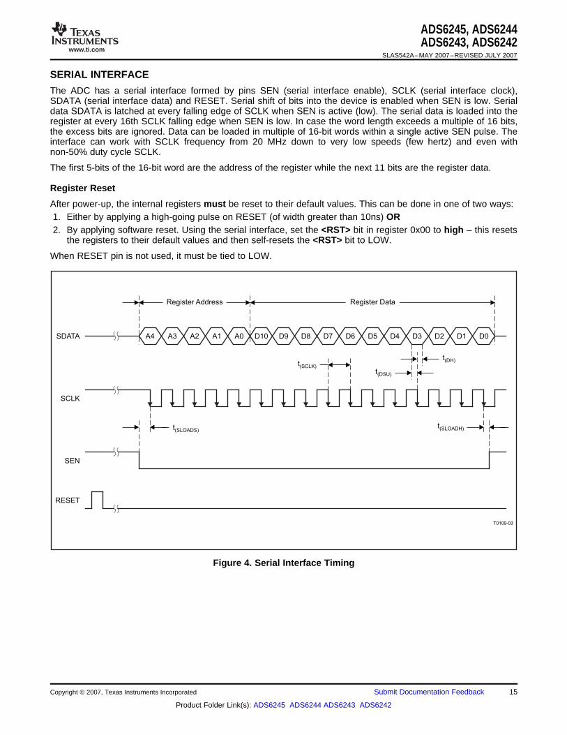
SERIAL INTERFACE
Register Reset
T0109-03
t(SCLK)t(DSU)
t(DH)
t(SLOADS)
D7A4 D3A0 D5A2 D1D9 D6A3 D2D10 D4A1 D0D8SDATA
SCLK
SEN
RESET
t(SLOADH)
Register Address Register Data
ADS6245, ADS6244ADS6243, ADS6242
SLAS542A–MAY 2007–REVISED JULY 2007
The ADC has a serial interface formed by pins SEN (serial interface enable), SCLK (serial interface clock),SDATA (serial interface data) and RESET. Serial shift of bits into the device is enabled when SEN is low. Serialdata SDATA is latched at every falling edge of SCLK when SEN is active (low). The serial data is loaded into theregister at every 16th SCLK falling edge when SEN is low. In case the word length exceeds a multiple of 16 bits,the excess bits are ignored. Data can be loaded in multiple of 16-bit words within a single active SEN pulse. Theinterface can work with SCLK frequency from 20 MHz down to very low speeds (few hertz) and even withnon-50% duty cycle SCLK.
The first 5-bits of the 16-bit word are the address of the register while the next 11 bits are the register data.
After power-up, the internal registers must be reset to their default values. This can be done in one of two ways:1. Either by applying a high-going pulse on RESET (of width greater than 10ns) OR2. By applying software reset. Using the serial interface, set the <RST> bit in register 0x00 to high – this resets
the registers to their default values and then self-resets the <RST> bit to LOW.
When RESET pin is not used, it must be tied to LOW.
Figure 4. Serial Interface Timing
Copyright © 2007, Texas Instruments Incorporated Submit Documentation Feedback 15
Product Folder Link(s): ADS6245 ADS6244 ADS6243 ADS6242
www.ti.com
SERIAL INTERFACE TIMING CHARACTERISTICS
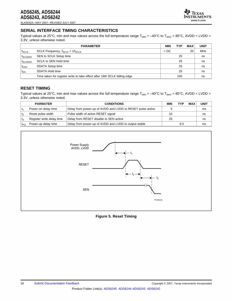
RESET TIMING
T0108-03
t1
t3
t2
Power SupplyAVDD, LVDD
RESET
SEN
ADS6245, ADS6244ADS6243, ADS6242SLAS542A–MAY 2007–REVISED JULY 2007
Typical values at 25°C, min and max values across the full temperature range TMIN = –40°C to TMAX = 85°C, AVDD = LVDD =3.3V, unless otherwise noted.
PARAMETER MIN TYP MAX UNIT
fSCLK SCLK Frequency, fSCLK = 1/tSCLK > DC 20 MHz
tSLOADS SEN to SCLK Setup time 25 ns
tSLOADH SCLK to SEN Hold time 25 ns
tDSU SDATA Setup time 25 ns
tDH SDATA Hold time 25 ns
Time taken for register write to take effect after 16th SCLK falling edge 100 ns
Typical values at 25°C, min and max values across the full temperature range TMIN = –40°C to TMAX = 85°C, AVDD = LVDD =3.3V, unless otherwise noted.
PARMATER CONDITIONS MIN TYP MAX UNIT
t1 Power-on delay time Delay from power-up of AVDD and LVDD to RESET pulse active 5 ms
t2 Reset pulse width Pulse width of active RESET signal 10 ns
t3 Register write delay time Delay from RESET disable to SEN active 25 ns
tPO Power-up delay time Delay from power-up of AVDD and LVDD to output stable 6.5 ms
Figure 5. Reset Timing
16 Submit Documentation Feedback Copyright © 2007, Texas Instruments Incorporated
Product Folder Link(s): ADS6245 ADS6244 ADS6243 ADS6242
www.ti.com
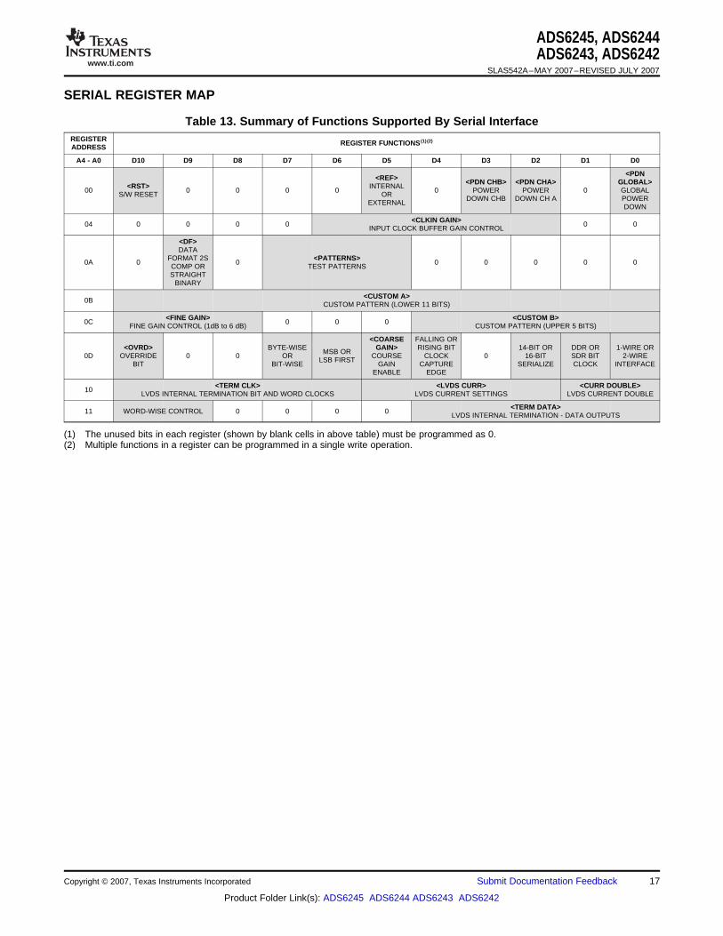
SERIAL REGISTER MAP
ADS6245, ADS6244ADS6243, ADS6242
SLAS542A–MAY 2007–REVISED JULY 2007
Table 13. Summary of Functions Supported By Serial InterfaceREGISTER REGISTER FUNCTIONS (1)(2)ADDRESS
A4 - A0 D10 D9 D8 D7 D6 D5 D4 D3 D2 D1 D0
<PDN<REF> <PDN CHB> <PDN CHA> GLOBAL><RST> INTERNAL00 0 0 0 0 0 POWER POWER 0 GLOBAL
S/W RESET ORDOWN CHB DOWN CH A POWER
EXTERNALDOWN
<CLKIN GAIN>04 0 0 0 0 0 0
INPUT CLOCK BUFFER GAIN CONTROL
<DF>DATA
FORMAT 2S <PATTERNS>0A 0 0 0 0 0 0 0
COMP OR TEST PATTERNSSTRAIGHT
BINARY
<CUSTOM A>0B
CUSTOM PATTERN (LOWER 11 BITS)
<FINE GAIN> <CUSTOM B>0C 0 0 0
FINE GAIN CONTROL (1dB to 6 dB) CUSTOM PATTERN (UPPER 5 BITS)
<COARSE FALLING OR<OVRD> BYTE-WISE GAIN> RISING BIT 14-BIT OR DDR OR 1-WIRE OR
MSB OR0D OVERRIDE 0 0 OR COURSE CLOCK 0 16-BIT SDR BIT 2-WIRE
LSB FIRSTBIT BIT-WISE GAIN CAPTURE SERIALIZE CLOCK INTERFACE
ENABLE EDGE
<TERM CLK> <LVDS CURR> <CURR DOUBLE>10
LVDS INTERNAL TERMINATION BIT AND WORD CLOCKS LVDS CURRENT SETTINGS LVDS CURRENT DOUBLE
<TERM DATA>11 WORD-WISE CONTROL 0 0 0 0
LVDS INTERNAL TERMINATION - DATA OUTPUTS
(1) The unused bits in each register (shown by blank cells in above table) must be programmed as 0.(2) Multiple functions in a register can be programmed in a single write operation.
Copyright © 2007, Texas Instruments Incorporated Submit Documentation Feedback 17
Product Folder Link(s): ADS6245 ADS6244 ADS6243 ADS6242
www.ti.com
DESCRIPTION OF SERIAL REGISTERS
ADS6245, ADS6244ADS6243, ADS6242SLAS542A–MAY 2007–REVISED JULY 2007
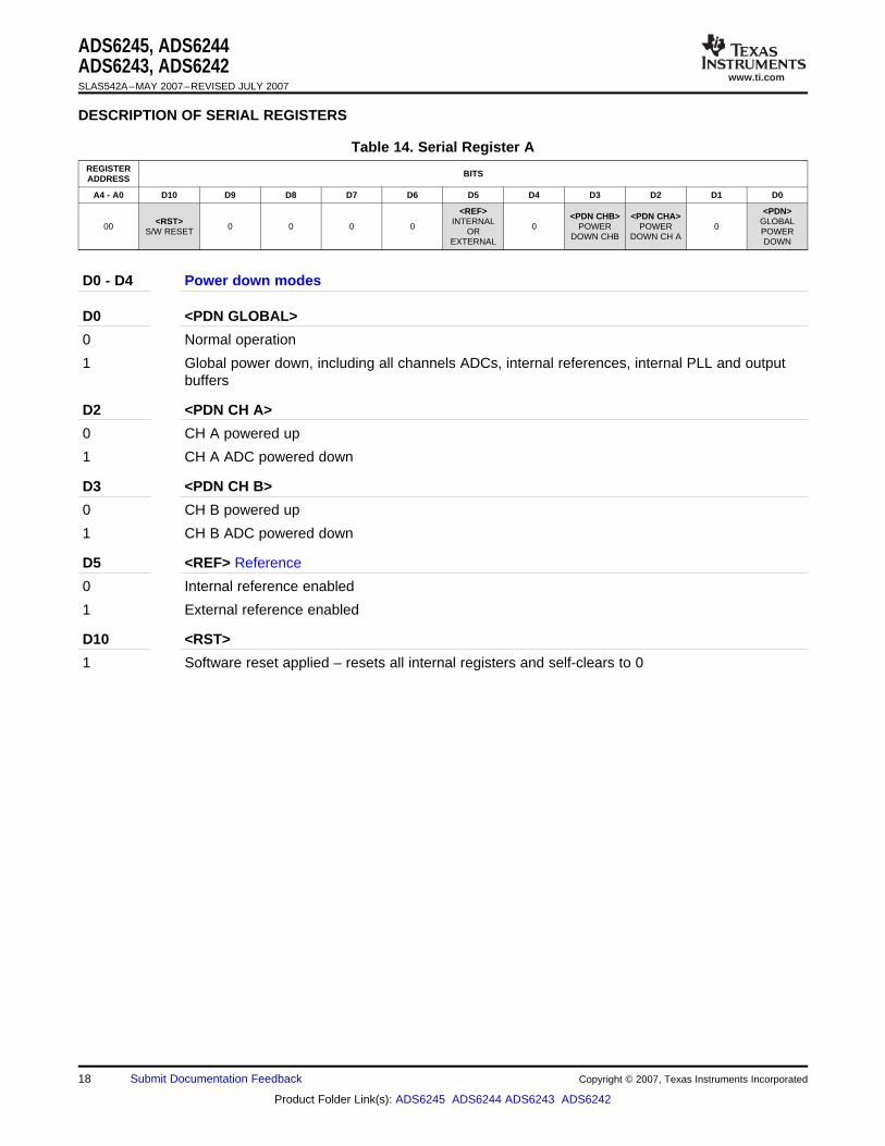
Table 14. Serial Register AREGISTER BITSADDRESS
A4 - A0 D10 D9 D8 D7 D6 D5 D4 D3 D2 D1 D0
<REF> <PDN><PDN CHB> <PDN CHA><RST> INTERNAL GLOBAL00 0 0 0 0 0 POWER POWER 0
S/W RESET OR POWERDOWN CHB DOWN CH A
EXTERNAL DOWN
D0 - D4 Power down modes
D0 <PDN GLOBAL>
0 Normal operation
1 Global power down, including all channels ADCs, internal references, internal PLL and outputbuffers
D2 <PDN CH A>
0 CH A powered up
1 CH A ADC powered down
D3 <PDN CH B>
0 CH B powered up
1 CH B ADC powered down
D5 <REF> Reference
0 Internal reference enabled
1 External reference enabled
D10 <RST>
1 Software reset applied – resets all internal registers and self-clears to 0
18 Submit Documentation Feedback Copyright © 2007, Texas Instruments Incorporated
Product Folder Link(s): ADS6245 ADS6244 ADS6243 ADS6242
www.ti.com
ADS6245, ADS6244ADS6243, ADS6242
SLAS542A–MAY 2007–REVISED JULY 2007
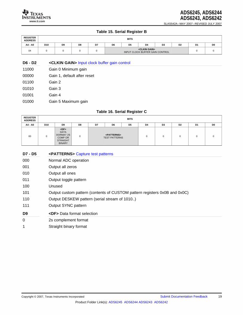
Table 15. Serial Register BREGISTER BITSADDRESS
A4 - A0 D10 D9 D8 D7 D6 D5 D4 D3 D2 D1 D0
<CLKIN GAIN>04 0 0 0 0 0 0
INPUT CLOCK BUFFER GAIN CONTROL
D6 - D2 <CLKIN GAIN> Input clock buffer gain control
11000 Gain 0 Minimum gain
00000 Gain 1, default after reset
01100 Gain 2
01010 Gain 3
01001 Gain 4
01000 Gain 5 Maximum gain
Table 16. Serial Register CREGISTER BITSADDRESS
A4 - A0 D10 D9 D8 D7 D6 D5 D4 D3 D2 D1 D0
<DF>DATA
DORMAT 2S <PATTERNS>00 0 0 0 0 0 0 0
COMP OR TEST PATTERNSSTRAIGHT
BINARY
D7 - D5 <PATTERNS> Capture test patterns
000 Normal ADC operation
001 Output all zeros
010 Output all ones
011 Output toggle pattern
100 Unused
101 Output custom pattern (contents of CUSTOM pattern registers 0x0B and 0x0C)
110 Output DESKEW pattern (serial stream of 1010..)
111 Output SYNC pattern
D9 <DF> Data format selection
0 2s complement format
1 Straight binary format
Copyright © 2007, Texas Instruments Incorporated Submit Documentation Feedback 19
Product Folder Link(s): ADS6245 ADS6244 ADS6243 ADS6242
www.ti.com
ADS6245, ADS6244ADS6243, ADS6242SLAS542A–MAY 2007–REVISED JULY 2007
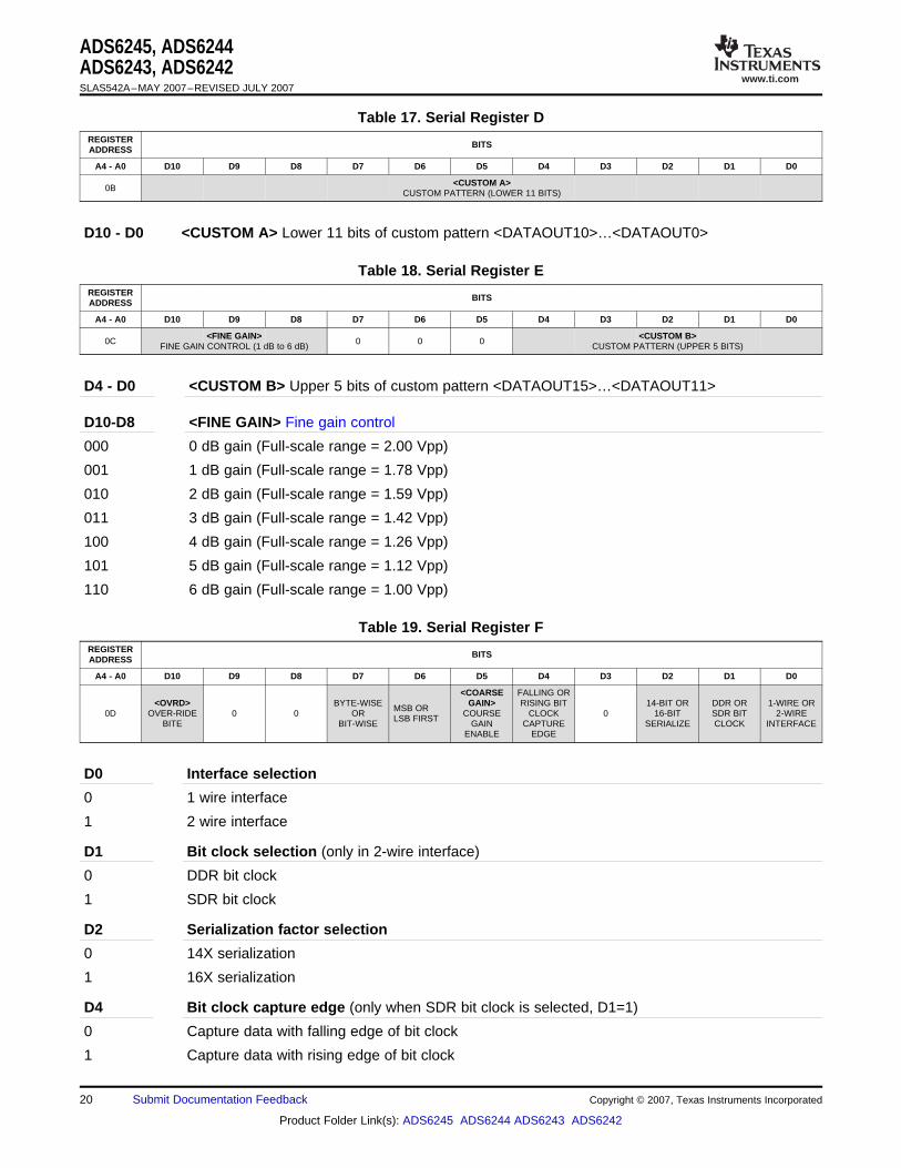
Table 17. Serial Register DREGISTER BITSADDRESS
A4 - A0 D10 D9 D8 D7 D6 D5 D4 D3 D2 D1 D0
<CUSTOM A>0B
CUSTOM PATTERN (LOWER 11 BITS)
D10 - D0 <CUSTOM A> Lower 11 bits of custom pattern <DATAOUT10>…<DATAOUT0>
Table 18. Serial Register EREGISTER BITSADDRESS
A4 - A0 D10 D9 D8 D7 D6 D5 D4 D3 D2 D1 D0
<FINE GAIN> <CUSTOM B>0C 0 0 0
FINE GAIN CONTROL (1 dB to 6 dB) CUSTOM PATTERN (UPPER 5 BITS)
D4 - D0 <CUSTOM B> Upper 5 bits of custom pattern <DATAOUT15>…<DATAOUT11>
D10-D8 <FINE GAIN> Fine gain control
000 0 dB gain (Full-scale range = 2.00 Vpp)
001 1 dB gain (Full-scale range = 1.78 Vpp)
010 2 dB gain (Full-scale range = 1.59 Vpp)
011 3 dB gain (Full-scale range = 1.42 Vpp)
100 4 dB gain (Full-scale range = 1.26 Vpp)
101 5 dB gain (Full-scale range = 1.12 Vpp)
110 6 dB gain (Full-scale range = 1.00 Vpp)
Table 19. Serial Register FREGISTER BITSADDRESS
A4 - A0 D10 D9 D8 D7 D6 D5 D4 D3 D2 D1 D0
<COARSE FALLING OR<OVRD> BYTE-WISE GAIN> RISING BIT 14-BIT OR DDR OR 1-WIRE OR
MSB OR0D OVER-RIDE 0 0 OR COURSE CLOCK 0 16-BIT SDR BIT 2-WIRE
LSB FIRSTBITE BIT-WISE GAIN CAPTURE SERIALIZE CLOCK INTERFACE
ENABLE EDGE
D0 Interface selection
0 1 wire interface
1 2 wire interface
D1 Bit clock selection (only in 2-wire interface)
0 DDR bit clock
1 SDR bit clock
D2 Serialization factor selection
0 14X serialization
1 16X serialization
D4 Bit clock capture edge (only when SDR bit clock is selected, D1=1)
0 Capture data with falling edge of bit clock
1 Capture data with rising edge of bit clock
20 Submit Documentation Feedback Copyright © 2007, Texas Instruments Incorporated
Product Folder Link(s): ADS6245 ADS6244 ADS6243 ADS6242
www.ti.com
ADS6245, ADS6244ADS6243, ADS6242
SLAS542A–MAY 2007–REVISED JULY 2007
D5 <COARSE GAIN>Coarse gain control
0 0 dB coarse gain
1 3.5dB coarse gain (Full-scale range = 1.34 Vpp)
D6 MSB or LSB first selection
0 MSB First
1 LSB First
D7 Byte/bit wise outputs (only when 2-wire is selected)
0 Byte wise
1 Bit wise
D10 <OVRD> Over-ride bit. All the functions in register 0x0D can also be controlled using theparallel control pins. By setting bit <OVRD> =1, the contents of register 0x0D will over-ride thesettings of the parallel pins.
0 Disable over-ride
1 Enable over-ride
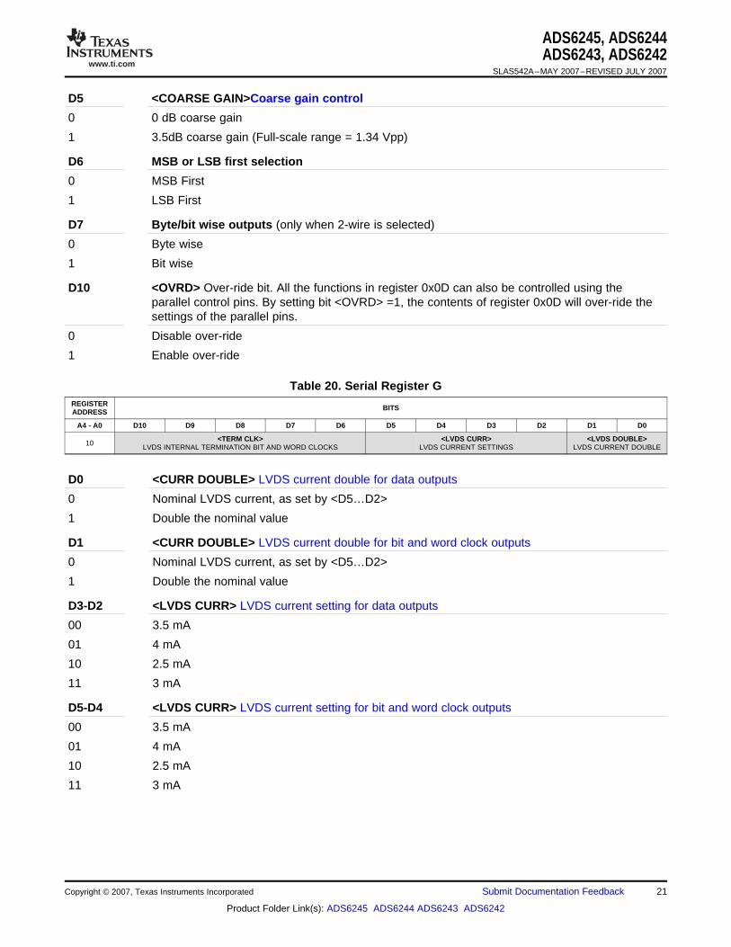
Table 20. Serial Register GREGISTER BITSADDRESS
A4 - A0 D10 D9 D8 D7 D6 D5 D4 D3 D2 D1 D0
<TERM CLK> <LVDS CURR> <LVDS DOUBLE>10
LVDS INTERNAL TERMINATION BIT AND WORD CLOCKS LVDS CURRENT SETTINGS LVDS CURRENT DOUBLE
D0 <CURR DOUBLE> LVDS current double for data outputs
0 Nominal LVDS current, as set by <D5…D2>
1 Double the nominal value
D1 <CURR DOUBLE> LVDS current double for bit and word clock outputs
0 Nominal LVDS current, as set by <D5…D2>
1 Double the nominal value
D3-D2 <LVDS CURR> LVDS current setting for data outputs
00 3.5 mA
01 4 mA
10 2.5 mA
11 3 mA
D5-D4 <LVDS CURR> LVDS current setting for bit and word clock outputs
00 3.5 mA
01 4 mA
10 2.5 mA
11 3 mA
Copyright © 2007, Texas Instruments Incorporated Submit Documentation Feedback 21
Product Folder Link(s): ADS6245 ADS6244 ADS6243 ADS6242

www.ti.com
ADS6245, ADS6244ADS6243, ADS6242SLAS542A–MAY 2007–REVISED JULY 2007
D10-D6 <TERM CLK> LVDS internal termination for bit and word clock outputs
00000 No internal termination
00001 166 Ω00010 200 Ω00100 250 Ω01000 333 Ω10000 500 Ω
Any combination of above bits can also be programmed, resulting in a parallel combination ofthe selected values. For example, 00101 is the parallel combination of 166||250 = 100 Ω
00101 100 Ω
Table 21. Serial Register HREGISTER BITSADDRESS
A4 - A0 D10 D9 D8 D7 D6 D5 D4 D3 D2 D1 D0
<TERM DATA>11 WORD-WISE CONTROL 0 0 0 0
LVDS INTERNAL TERMINATION - DATA OUTPUTS
D4-D0 <TERM DATA> LVDS internal termination for data outputs
00000 No internal termination
00001 166 Ω00010 200 Ω00100 250 Ω01000 333 Ω10000 500 Ω
Any combination of above bits can also be programmed, resulting in a parallel combination ofthe selected values. For example, 00101 is the parallel combination of 166||250 = 100 Ω
00101 100 Ω
D10-D9 Only when 2-wire interface is selected
00 Byte-wise or bit-wise output, 1x frame clock
11 Word-wise output enabled, 0.5x frame clock
01,10 Do not use
22 Submit Documentation Feedback Copyright © 2007, Texas Instruments Incorporated
Product Folder Link(s): ADS6245 ADS6244 ADS6243 ADS6242
www.ti.com
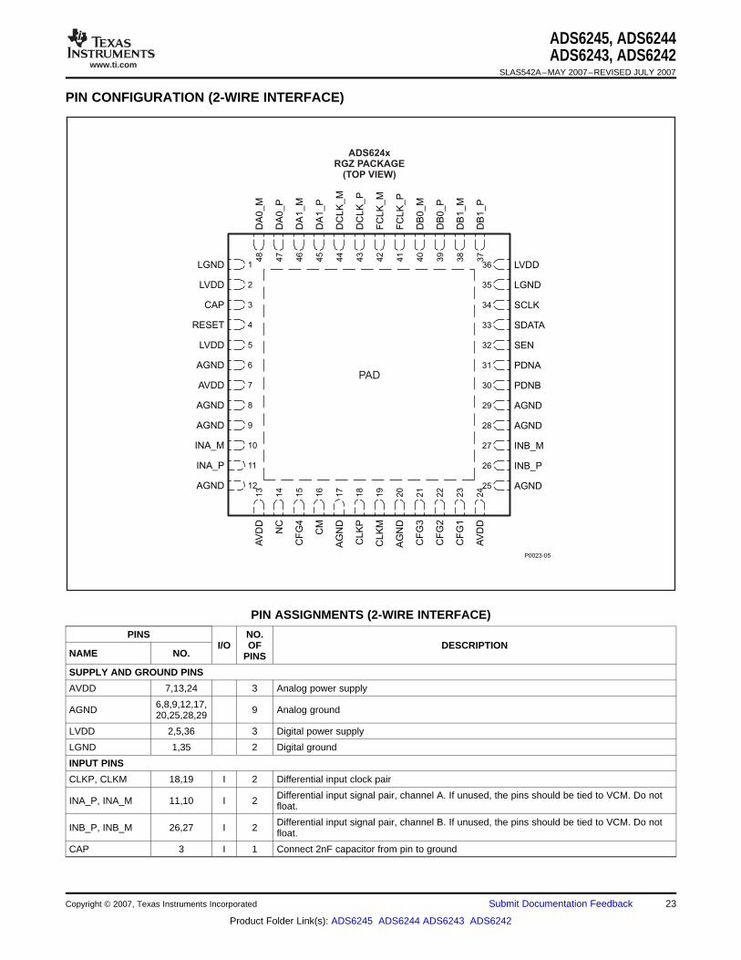
PIN CONFIGURATION (2-WIRE INTERFACE)
P0023-05
ADS624xRGZ PACKAGE
(TOP VIEW)
LGNDA
VD
D
LVDDN
C
CAPC
FG
4
RESETC
M
LVDDA
GN
D
AGNDC
LK
P
AVDDC
LK
M
AGNDA
GN
D
AGNDC
FG
3
INA_MC
FG
2
INA_PC
FG
1
AGNDA
VD
D
1
2
3
4
5
6
7
8
9
10
11
12
13
14
15
16
17
18
19
20
21
22
23
24
LVDDD
A0
_M
LGNDD
A0_P
SCLKD
A1_M
SDATAD
A1
_P
SEND
CL
K_
M
PDNAD
CL
K_
P
PDNBF
CL
K_
M
AGNDF
CLK
_P
AGNDD
B0
_M
INB_MD
B0_P
INB_PD
B1_M
AGNDD
B1_P
36
35
34
33
32
31
30
29
28
27
26
25
48
47
46
45
44
43
42
41
40
39
38
37
PAD
ADS6245, ADS6244ADS6243, ADS6242
SLAS542A–MAY 2007–REVISED JULY 2007
PIN ASSIGNMENTS (2-WIRE INTERFACE)
PINS NO.I/O OF DESCRIPTION
NAME NO. PINS
SUPPLY AND GROUND PINS
AVDD 7,13,24 3 Analog power supply
6,8,9,12,17,AGND 9 Analog ground20,25,28,29
LVDD 2,5,36 3 Digital power supply
LGND 1,35 2 Digital ground
INPUT PINS
CLKP, CLKM 18,19 I 2 Differential input clock pair
Differential input signal pair, channel A. If unused, the pins should be tied to VCM. Do notINA_P, INA_M 11,10 I 2 float.
Differential input signal pair, channel B. If unused, the pins should be tied to VCM. Do notINB_P, INB_M 26,27 I 2 float.
CAP 3 I 1 Connect 2nF capacitor from pin to ground
Copyright © 2007, Texas Instruments Incorporated Submit Documentation Feedback 23
Product Folder Link(s): ADS6245 ADS6244 ADS6243 ADS6242

www.ti.com
ADS6245, ADS6244ADS6243, ADS6242SLAS542A–MAY 2007–REVISED JULY 2007
PIN ASSIGNMENTS (2-WIRE INTERFACE) (continued)
PINS NO.I/O OF DESCRIPTION
NAME NO. PINS
This pin functions as serial interface clock input when RESET is low.When RESET is high, it controls DESKEW, SYNC and global POWER DOWN modesSCLK 34 I 1 (along with SDATA). See Table 5 for description.This pin has an internal pull-down resistor.
This pin functions as serial interface data input when RESET is low.When RESET is high, it controls DESKEW, SYNC and global POWER DOWN modesSDATA 33 I 1 (along with SCLK). See Table 5 for description.This pin has an internal pull-down resistor.
This pin functions as serial interface enable input when RESET is low.When RESET is high, it controls coarse gain and internal/external reference modes. SeeSEN 32 I 1 Table 6 for description.This pin has an internal pull-up resistor.
Serial interface reset input.
When using the serial interface mode, the user MUST initialize internal registers throughhardware RESET by applying a high-going pulse on this pin or by using software resetRESET 4 I 1 option. Refer to the Serial Interface section. In parallel interface mode, tie RESETpermanently high. (SCLK, SDATA and SEN function as parallel control pins in this mode).
The pin has an internal pull-down resistor to ground.
PDNA 31 I 1 Channel A ADC power down control pin.
PDNB 30 I 1 Channel B ADC power down control pin.
Parallel input pin. It controls 1-wire or 2-wire interface and DDR or SDR bit clock selection.CFG1 23 I 1 See Table 9 for description.
Tie to AVDD for 2-wire interface with DDR bit clock.
Parallel input pin. It controls 12x or 14x serialization and SDR bit clock capture edge. SeeCFG2 22 I 1 Table 10 for description.
For 12x serialization with DDR bit clock, tie to ground or AVDD.
CFG3 21 I 1 RESERVED pin - Tie to ground.
Parallel input pin. It controls data format and MSB or LSB first modes. See Table 12 forCFG4 15 I 1 description.
Internal reference mode – common-mode voltage outputVCM 16 IO 1 External reference mode – reference input. The voltage forced on this pin sets the internal
reference.
OUTPUT PINS
DA0_P,DA0_M 47,48 O 2 Channel A differential LVDS data output pair, wire 0
DA1_P,DA1_M 45,46 O 2 Channel A differential LVDS data output pair, wire 1
DB0_P,DB0_M 39,40 O 2 Channel B differential LVDS data output pair, wire 0
DB1_P,DB1_M 37,38 O 2 Channel B differential LVDS data output pair, wire 1
DCLKP,DCLKM 43,44 O 2 Differential bit clock output pair
FCLKP,FCLKM 41,42 O 2 Differential frame clock output pair
NC 14 1 Do Not Connect
Connect to ground using multiple vias. Refer to Board Design Considerations in applicationPAD 0 1 section.
24 Submit Documentation Feedback Copyright © 2007, Texas Instruments Incorporated
Product Folder Link(s): ADS6245 ADS6244 ADS6243 ADS6242
www.ti.com
PIN CONFIGURATION (1-WIRE INTERFACE)
P0023-06
ADS624xRGZ PACKAGE
(TOP VIEW)
LGNDA
VD
D
LVDDN
C
CAPC
FG
4
RESETC
M
LVDDA
GN
D
AGNDC
LK
P
AVDDC
LK
M
AGNDA
GN
D
AGNDC
FG
3
INA_MC
FG
2
INA_PC
FG
1
AGNDA
VD
D
1
2
3
4
5
6
7
8
9
10
11
12
13
14
15
16
17
18
19
20
21
22
23
24
LVDDU
NU
SE
D
LGNDU
NU
SE
D
SCLKD
A_M
SDATAD
A_
P
SEND
CL
K_
M
PDNAD
CL
K_
P
PDNBF
CL
K_
M
AGNDF
CLK
_P
AGNDD
B_
M
INB_MD
B_P
INB_PU
NU
SE
D
AGNDU
NU
SE
D
36
35
34
33
32
31
30
29
28
27
26
25
48
47
46
45
44
43
42
41
40
39
38
37
PAD
ADS6245, ADS6244ADS6243, ADS6242
SLAS542A–MAY 2007–REVISED JULY 2007
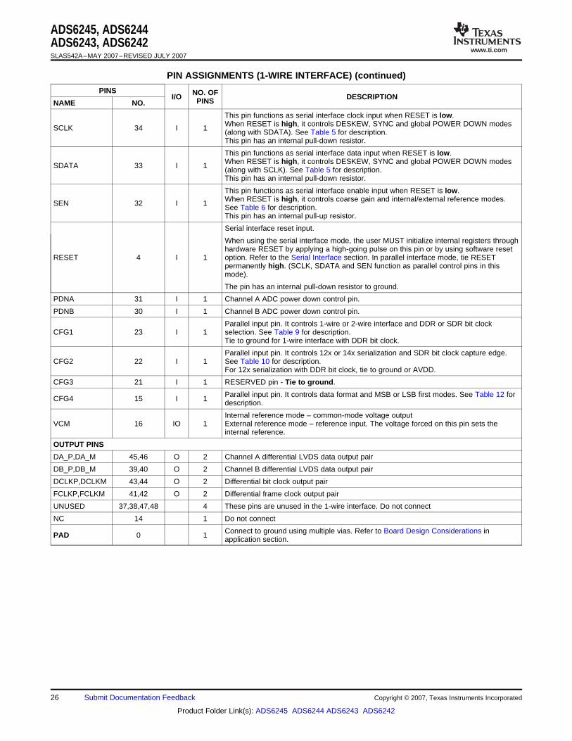
PIN ASSIGNMENTS (1-WIRE INTERFACE)
PINS NO. OFI/O DESCRIPTIONPINSNAME NO.
SUPPLY AND GROUND PINS
AVDD 7,13,24 3 Analog power supply
6,8,9,12,17,AGND 9 Analog ground20,25,28,29
LVDD 2,5,36 3 Digital power supply
LGND 1,35 2 Digital ground
INPUT PINS
CLKP, CLKM 18,19 I 2 Differential input clock pair
Differential input signal pair, channel A. If unused, the pins should be tied to VCM. DoINA_P, INA_M 11,10 I 2 not float.
Differential input signal pair, channel B. If unused, the pins should be tied to VCM. DoIND_P, IND_M 26,27 I I2 not float.
CAP 3 I 1 Connect 2nF capacitance from pin to ground
Copyright © 2007, Texas Instruments Incorporated Submit Documentation Feedback 25
Product Folder Link(s): ADS6245 ADS6244 ADS6243 ADS6242
www.ti.com
ADS6245, ADS6244ADS6243, ADS6242SLAS542A–MAY 2007–REVISED JULY 2007
PIN ASSIGNMENTS (1-WIRE INTERFACE) (continued)
PINS NO. OFI/O DESCRIPTIONPINSNAME NO.
This pin functions as serial interface clock input when RESET is low.When RESET is high, it controls DESKEW, SYNC and global POWER DOWN modesSCLK 34 I 1 (along with SDATA). See Table 5 for description.This pin has an internal pull-down resistor.
This pin functions as serial interface data input when RESET is low.When RESET is high, it controls DESKEW, SYNC and global POWER DOWN modesSDATA 33 I 1 (along with SCLK). See Table 5 for description.This pin has an internal pull-down resistor.
This pin functions as serial interface enable input when RESET is low.When RESET is high, it controls coarse gain and internal/external reference modes.SEN 32 I 1 See Table 6 for description.This pin has an internal pull-up resistor.
Serial interface reset input.
When using the serial interface mode, the user MUST initialize internal registers throughhardware RESET by applying a high-going pulse on this pin or by using software reset
RESET 4 I 1 option. Refer to the Serial Interface section. In parallel interface mode, tie RESETpermanently high. (SCLK, SDATA and SEN function as parallel control pins in thismode).
The pin has an internal pull-down resistor to ground.
PDNA 31 I 1 Channel A ADC power down control pin.
PDNB 30 I 1 Channel B ADC power down control pin.
Parallel input pin. It controls 1-wire or 2-wire interface and DDR or SDR bit clockCFG1 23 I 1 selection. See Table 9 for description.
Tie to ground for 1-wire interface with DDR bit clock.
Parallel input pin. It controls 12x or 14x serialization and SDR bit clock capture edge.CFG2 22 I 1 See Table 10 for description.
For 12x serialization with DDR bit clock, tie to ground or AVDD.
CFG3 21 I 1 RESERVED pin - Tie to ground.
Parallel input pin. It controls data format and MSB or LSB first modes. See Table 12 forCFG4 15 I 1 description.
Internal reference mode – common-mode voltage outputVCM 16 IO 1 External reference mode – reference input. The voltage forced on this pin sets the
internal reference.
OUTPUT PINS
DA_P,DA_M 45,46 O 2 Channel A differential LVDS data output pair
DB_P,DB_M 39,40 O 2 Channel B differential LVDS data output pair
DCLKP,DCLKM 43,44 O 2 Differential bit clock output pair
FCLKP,FCLKM 41,42 O 2 Differential frame clock output pair
UNUSED 37,38,47,48 4 These pins are unused in the 1-wire interface. Do not connect
NC 14 1 Do not connect
Connect to ground using multiple vias. Refer to Board Design Considerations inPAD 0 1 application section.
26 Submit Documentation Feedback Copyright © 2007, Texas Instruments Incorporated
Product Folder Link(s): ADS6245 ADS6244 ADS6243 ADS6242
www.ti.com
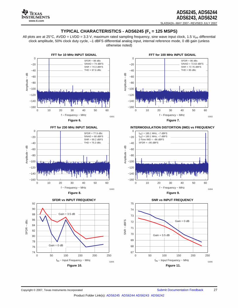
TYPICAL CHARACTERISTICS - ADS6245 (Fs = 125 MSPS)
f − Frequency − MHz
−160
−140
−120
−100
−80
−60
−40
−20
0
0 10 20 30 40 50 60
Am
plitu
de −
dB
G001
SFDR = 88 dBcSINAD = 74 dBFSSNR = 74.3 dBFSTHD = 87.6 dBc
f − Frequency − MHz
−160
−140
−120
−100
−80
−60
−40
−20
0
0 10 20 30 40 50 60
Am
plitu
de −
dB
G002
SFDR = 86 dBcSINAD = 72.63 dBFSSNR = 72.76 dBFSTHD = 85 dBc
f − Frequency − MHz
−160
−140
−120
−100
−80
−60
−40
−20
0
0 10 20 30 40 50 60
Am
plitu
de −
dB
G003
SFDR = 77.9 dBcSINAD = 68 dBFSSNR = 69.2 dBFSTHD = 75.3 dBc
f − Frequency − MHz
−160
−140
−120
−100
−80
−60
−40
−20
0
0 10 20 30 40 50 60
Am
plitu
de −
dB
G004
fIN1 = 185.1 MHz, –7 dBFSfIN2 = 190.1 MHz, –7 dBFS2-Tone IMD = –86 dBFSSFDR = –95 dBFS
fIN − Input Frequency − MHz
74
76
78
80
82
84
86
88
90
92
0 50 100 150 200 250
SF
DR
− d
Bc
G005
Gain = 0 dB
Gain = 3.5 dB
fIN − Input Frequency − MHz
67
68
69
70
71
72
73
74
75
0 50 100 150 200 250
SN
R −
dB
FS
G006
Gain = 0 dB
Gain = 3.5 dB
ADS6245, ADS6244ADS6243, ADS6242
SLAS542A–MAY 2007–REVISED JULY 2007
All plots are at 25°C, AVDD = LVDD = 3.3 V, maximum rated sampling frequency, sine wave input clock, 1.5 VPP differentialclock amplitude, 50% clock duty cycle, –1 dBFS differential analog input, internal reference mode, 0 dB gain (unless
otherwise noted)
FFT for 10 MHz INPUT SIGNAL FFT for 100 MHz INPUT SIGNAL
Figure 6. Figure 7.
FFT for 230 MHz INPUT SIGNAL INTERMODULATION DISTORTION (IMD) vs FREQUENCY
Figure 8. Figure 9.
SFDR vs INPUT FREQUENCY SNR vs INPUT FREQUENCY
Figure 10. Figure 11.
Copyright © 2007, Texas Instruments Incorporated Submit Documentation Feedback 27
Product Folder Link(s): ADS6245 ADS6244 ADS6243 ADS6242

www.ti.com
fIN − Input Frequency − MHz
74
76
78
80
82
84
86
88
90
92
10 30 50 70 90 110 130 150 170 190 210 230
SF
DR
− d
Bc
G007
Input adjusted to get −1dBFS input
1 dB0 dB
2 dB
4 dB
5 dB
6 dB
3 dB
fIN − Input Frequency − MHz
65
66
67
68
69
70
71
72
73
74
75
20 40 60 80 100 120 140 160 180 200 220
SIN
AD
− d
BF
S
G008
2 dB
5 dB
1 dB
0 dB
3 dB
3.5 dB
4 dB
6 dB
SN
R −
dB
FS
70
71
72
73
74
75
76
77
78
AVDD − Supply Voltage − V
72
74
76
78
80
82
84
86
88
3.0 3.1 3.2 3.3 3.4 3.5 3.6
SF
DR
− d
Bc
G009
SNR
SFDRfIN = 50.1 MHzLVDD = 3.3 V
SN
R −
dB
FS
70
71
72
73
74
75
LVDD − Supply Voltage − V
78
82
86
90
94
98
3.0 3.1 3.2 3.3 3.4 3.5 3.6
SF
DR
− d
Bc
G010
fIN = 50.1 MHzAVDD = 3.3 V
SNR
SFDR
70
71
72
73
74
75
76
77
78
Input Amplitude − dBFS
30
40
50
60
70
80
90
100
110
−60 −50 −40 −30 −20 −10 0
fIN = 20 MHz
SF
DR
− d
Bc,
dB
FS
G012
SN
R −
dB
FS
SFDR (dBc)
SFDR (dBFS)
SNR (dBFS)
SN
R −
dB
FS
71
72
73
74
75
76
77
T − Temperature − °C
74
76
78
80
82
84
86
−40 −20 0 20 40 60 80
SF
DR
− d
Bc
G011
fIN = 50.1 MHz
SNR
SFDR
ADS6245, ADS6244ADS6243, ADS6242SLAS542A–MAY 2007–REVISED JULY 2007
TYPICAL CHARACTERISTICS - ADS6245 (Fs = 125 MSPS) (continued)All plots are at 25°C, AVDD = LVDD = 3.3 V, maximum rated sampling frequency, sine wave input clock, 1.5 VPP differentialclock amplitude, 50% clock duty cycle, –1 dBFS differential analog input, internal reference mode, 0 dB gain (unlessotherwise noted)
SFDR vs INPUT FREQUENCY ACROSS GAINS SINAD vs INPUT FREQUENCY ACROSS GAINS
Figure 12. Figure 13.
PERFORMANCE vs AVDD PERFORMANCE vs LVDD
Figure 14. Figure 15.
PERFORMANCE vs TEMPERATURE PERFORMANCE vs INPUT AMPLITUDE
Figure 16. Figure 17.
28 Submit Documentation Feedback Copyright © 2007, Texas Instruments Incorporated
Product Folder Link(s): ADS6245 ADS6244 ADS6243 ADS6242

www.ti.com
SN
R −
dB
FS
70
71
72
73
74
75
76
77
72
74
76
78
80
82
84
86
0.5 1.0 1.5 2.0 2.5 3.0
SF
DR
− d
Bc
Input Clock Amplitude − VPP G013
SNR
SFDR
fIN = 50.1 MHz
SN
R −
dB
FS
72
73
74
75
76
77
78
Input Clock Duty Cycle − %
84
85
86
87
88
89
90
35 40 45 50 55 60 65
SF
DR
− d
Bc
G014
SNR
SFDR
fIN = 20.1 MHz
fS − Sampling Frequency − MSPS
0.0
0.1
0.2
0.3
0.4
0.5
0.6
0.7
0.8
0.9
1.0
0 25 50 75 100 125
PD
− P
ower
Dis
sipa
tion
− W
G015
LVDD
AVDD
Output Code
0
5
10
15
20
25
30
35
40
8187 8188 8189 8190 8191 8192 8193 8194 8195 8196
Occ
uren
ce −
%
G016
RMS (LSB) = 1.064
f − Frequency − MHz
−100
−90
−80
−70
−60
−50
−40
−30
−20
−10
0
0 50 100 150 200 250 300
CM
RR
− C
omm
on-M
ode
Rej
ectio
n R
atio
− d
Bc
G018
SN
R −
dB
FS
68
70
72
74
76
78
VVCM − VCM Voltage − V
84
86
88
90
92
94
1.30 1.35 1.40 1.45 1.50 1.55 1.60 1.65 1.70
fIN = 50.1 MHzExternal Reference Mode
SF
DR
− d
Bc
G017
SNR
SFDR
ADS6245, ADS6244ADS6243, ADS6242
SLAS542A–MAY 2007–REVISED JULY 2007
TYPICAL CHARACTERISTICS - ADS6245 (Fs = 125 MSPS) (continued)All plots are at 25°C, AVDD = LVDD = 3.3 V, maximum rated sampling frequency, sine wave input clock, 1.5 VPP differentialclock amplitude, 50% clock duty cycle, –1 dBFS differential analog input, internal reference mode, 0 dB gain (unlessotherwise noted)
PERFORMANCE vs CLOCK AMPLITUDE PERFORMANCE vs CLOCK DUTY CYCLE
Figure 18. Figure 19.
OUTPUT NOISE HISTOGRAM WITHPOWER DISSIPATION vs SAMPLING FREQUENCY INPUTS TIED TO COMMON-MODE
Figure 20. Figure 21.
PERFORMANCE IN EXTERNAL REFERENCE MODE CMRR vs FREQUENCY
Figure 22. Figure 23.
Copyright © 2007, Texas Instruments Incorporated Submit Documentation Feedback 29
Product Folder Link(s): ADS6245 ADS6244 ADS6243 ADS6242
www.ti.com
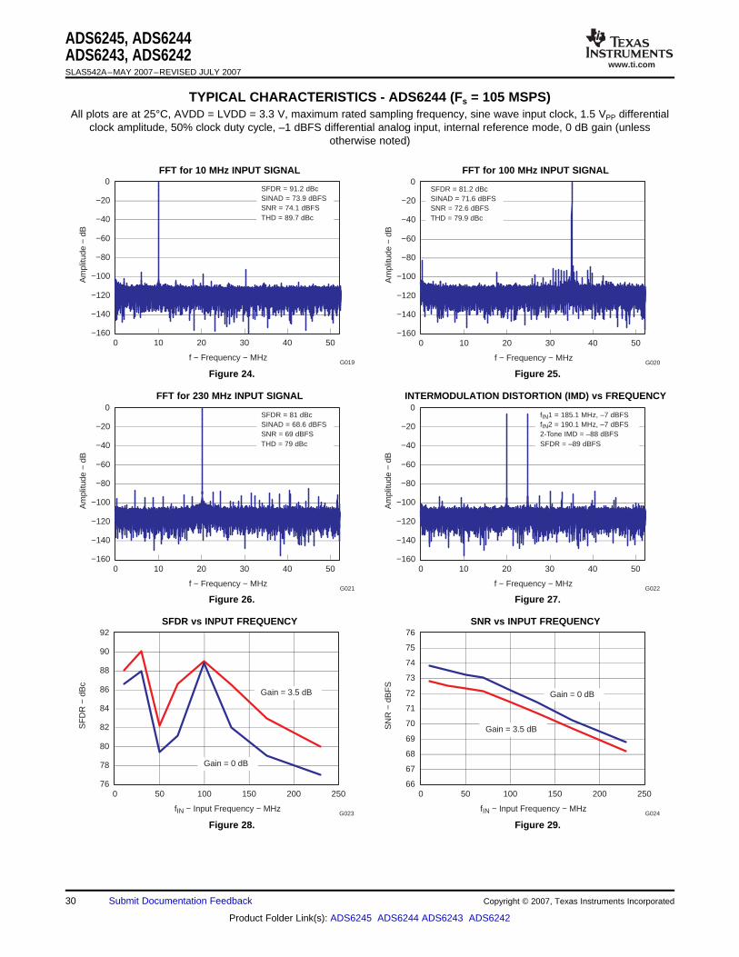
TYPICAL CHARACTERISTICS - ADS6244 (Fs = 105 MSPS)
f − Frequency − MHz
−160
−140
−120
−100
−80
−60
−40
−20
0
0 10 20 30 40 50
Am
plitu
de −
dB
G019
SFDR = 91.2 dBcSINAD = 73.9 dBFSSNR = 74.1 dBFSTHD = 89.7 dBc
f − Frequency − MHz
−160
−140
−120
−100
−80
−60
−40
−20
0
0 10 20 30 40 50
Am
plitu
de −
dB
G020
SFDR = 81.2 dBcSINAD = 71.6 dBFSSNR = 72.6 dBFSTHD = 79.9 dBc
f − Frequency − MHz
−160
−140
−120
−100
−80
−60
−40
−20
0
0 10 20 30 40 50
Am
plitu
de −
dB
G021
SFDR = 81 dBcSINAD = 68.6 dBFSSNR = 69 dBFSTHD = 79 dBc
f − Frequency − MHz
−160
−140
−120
−100
−80
−60
−40
−20
0
0 10 20 30 40 50
Am
plitu
de −
dB
G022
fIN1 = 185.1 MHz, –7 dBFSfIN2 = 190.1 MHz, –7 dBFS2-Tone IMD = –88 dBFSSFDR = –89 dBFS
fIN − Input Frequency − MHz
76
78
80
82
84
86
88
90
92
0 50 100 150 200 250
SF
DR
− d
Bc
G023
Gain = 0 dB
Gain = 3.5 dB
fIN − Input Frequency − MHz
66
67
68
69
70
71
72
73
74
75
76
0 50 100 150 200 250
SN
R −
dB
FS
G024
Gain = 0 dB
Gain = 3.5 dB
ADS6245, ADS6244ADS6243, ADS6242SLAS542A–MAY 2007–REVISED JULY 2007
All plots are at 25°C, AVDD = LVDD = 3.3 V, maximum rated sampling frequency, sine wave input clock, 1.5 VPP differentialclock amplitude, 50% clock duty cycle, –1 dBFS differential analog input, internal reference mode, 0 dB gain (unless
otherwise noted)
FFT for 10 MHz INPUT SIGNAL FFT for 100 MHz INPUT SIGNAL
Figure 24. Figure 25.
FFT for 230 MHz INPUT SIGNAL INTERMODULATION DISTORTION (IMD) vs FREQUENCY
Figure 26. Figure 27.
SFDR vs INPUT FREQUENCY SNR vs INPUT FREQUENCY
Figure 28. Figure 29.
30 Submit Documentation Feedback Copyright © 2007, Texas Instruments Incorporated
Product Folder Link(s): ADS6245 ADS6244 ADS6243 ADS6242
www.ti.com
fIN − Input Frequency − MHz
74
76
78
80
82
84
86
88
90
92
10 30 50 70 90 110 130 150 170 190 210 230
SF
DR
− d
Bc
G025
Input adjusted to get −1dBFS input
1 dB
6 dB
0 dB
2 dB
4 dB
3 dB
5 dB
fIN − Input Frequency − MHz
65
66
67
68
69
70
71
72
73
74
75
20 40 60 80 100 120 140 160 180 200 220
SIN
AD
− d
BF
S
G026
2 dB
5 dB
1 dB
0 dB
3 dB
3.5 dB
4 dB6 dB
SN
R −
dB
FS
70
71
72
73
74
75
LVDD − Supply Voltage − V
78
82
86
90
94
98
3.0 3.1 3.2 3.3 3.4 3.5 3.6
SF
DR
− d
Bc
G028
fIN = 70.1 MHzAVDD = 3.3 V
SNR
SFDR
SN
R −
dB
FS
70
71
72
73
74
75
76
77
78
AVDD − Supply Voltage − V
72
74
76
78
80
82
84
86
88
3.0 3.1 3.2 3.3 3.4 3.5 3.6
SF
DR
− d
Bc
G027
SNR
SFDR
fIN = 70.1 MHzLVDD = 3.3 V
SN
R −
dB
FS
71
72
73
74
75
76
77
T − Temperature − °C
74
76
78
80
82
84
86
−40 −20 0 20 40 60 80
SF
DR
− d
Bc
G029
fIN = 70.1 MHz
SNR
SFDR
50
55
60
65
70
75
80
85
90
Input Amplitude − dBFS
30
40
50
60
70
80
90
100
110
−60 −50 −40 −30 −20 −10 0
fIN = 20 MHz
SF
DR
− d
Bc,
dB
FS
G030
SN
R −
dB
FS
SFDR (dBc)
SFDR (dBFS)
SNR (dBFS)
ADS6245, ADS6244ADS6243, ADS6242
SLAS542A–MAY 2007–REVISED JULY 2007
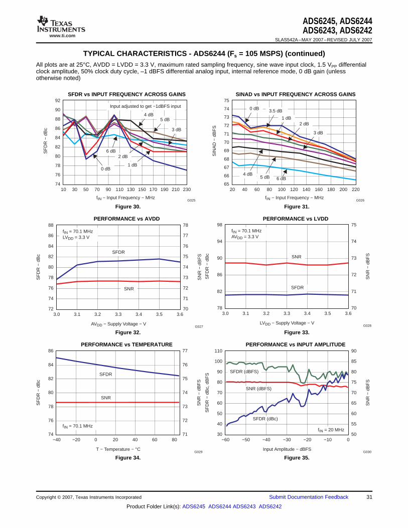
TYPICAL CHARACTERISTICS - ADS6244 (Fs = 105 MSPS) (continued)All plots are at 25°C, AVDD = LVDD = 3.3 V, maximum rated sampling frequency, sine wave input clock, 1.5 VPP differentialclock amplitude, 50% clock duty cycle, –1 dBFS differential analog input, internal reference mode, 0 dB gain (unlessotherwise noted)
SFDR vs INPUT FREQUENCY ACROSS GAINS SINAD vs INPUT FREQUENCY ACROSS GAINS
Figure 30. Figure 31.
PERFORMANCE vs AVDD PERFORMANCE vs LVDD
Figure 32. Figure 33.
PERFORMANCE vs TEMPERATURE PERFORMANCE vs INPUT AMPLITUDE
Figure 34. Figure 35.
Copyright © 2007, Texas Instruments Incorporated Submit Documentation Feedback 31
Product Folder Link(s): ADS6245 ADS6244 ADS6243 ADS6242

www.ti.com
SN
R −
dB
FS
71
72
73
74
75
76
Input Clock Duty Cycle − %
83
85
87
89
91
93
35 40 45 50 55 60 65
SF
DR
− d
Bc
G032
SNR
SFDR
fIN = 20.1 MHz
76
78
80
82
84
86
88
90
92
0.5 1.0 1.5 2.0 2.5 3.0
SF
DR
− d
Bc
SN
R −
dB
FS
68
69
70
71
72
73
74
75
76
Input Clock Amplitude − VPP G031
SNR
SFDR
fIN = 70.1 MHz
fS − Sampling Frequency − MSPS
0.0
0.1
0.2
0.3
0.4
0.5
0.6
0.7
0.8
0.9
1.0
0 20 40 60 80 100
PD
− P
ower
Dis
sipa
tion
− W
G033
LVDD
AVDD
Output Code
0
5
10
15
20
25
30
35
40
8179 8180 8181 8182 8183 8184 8185 8186 8187 8188
Occ
uren
ce −
%
G034
RMS (LSB) = 1.054
f − Frequency − MHz
−100
−90
−80
−70
−60
−50
−40
−30
−20
−10
0
0 50 100 150 200 250 300
CM
RR
− C
omm
on-M
ode
Rej
ectio
n R
atio
− d
Bc
G018
SN
R −
dB
FS
66
68
70
72
74
76
VVCM − VCM Voltage − V
80
81
82
83
84
85
1.30 1.35 1.40 1.45 1.50 1.55 1.60 1.65 1.70
fIN = 70.1 MHzExternal Reference Mode
SF
DR
− d
Bc
G035
SNR
SFDR
ADS6245, ADS6244ADS6243, ADS6242SLAS542A–MAY 2007–REVISED JULY 2007
TYPICAL CHARACTERISTICS - ADS6244 (Fs = 105 MSPS) (continued)All plots are at 25°C, AVDD = LVDD = 3.3 V, maximum rated sampling frequency, sine wave input clock, 1.5 VPP differentialclock amplitude, 50% clock duty cycle, –1 dBFS differential analog input, internal reference mode, 0 dB gain (unlessotherwise noted)
PERFORMANCE vs CLOCK AMPLITUDE PERFORMANCE vs CLOCK DUTY CYCLE
Figure 36. Figure 37.
OUTPUT NOISE HISTOGRAM WITHPOWER DISSIPATION vs SAMPLING FREQUENCY INPUTS TIED TO COMMON-MODE
Figure 38. Figure 39.
PERFORMANCE IN EXTERNAL REFERENCE MODE CMRR vs FREQUENCY
Figure 40. Figure 41.
32 Submit Documentation Feedback Copyright © 2007, Texas Instruments Incorporated
Product Folder Link(s): ADS6245 ADS6244 ADS6243 ADS6242
www.ti.com
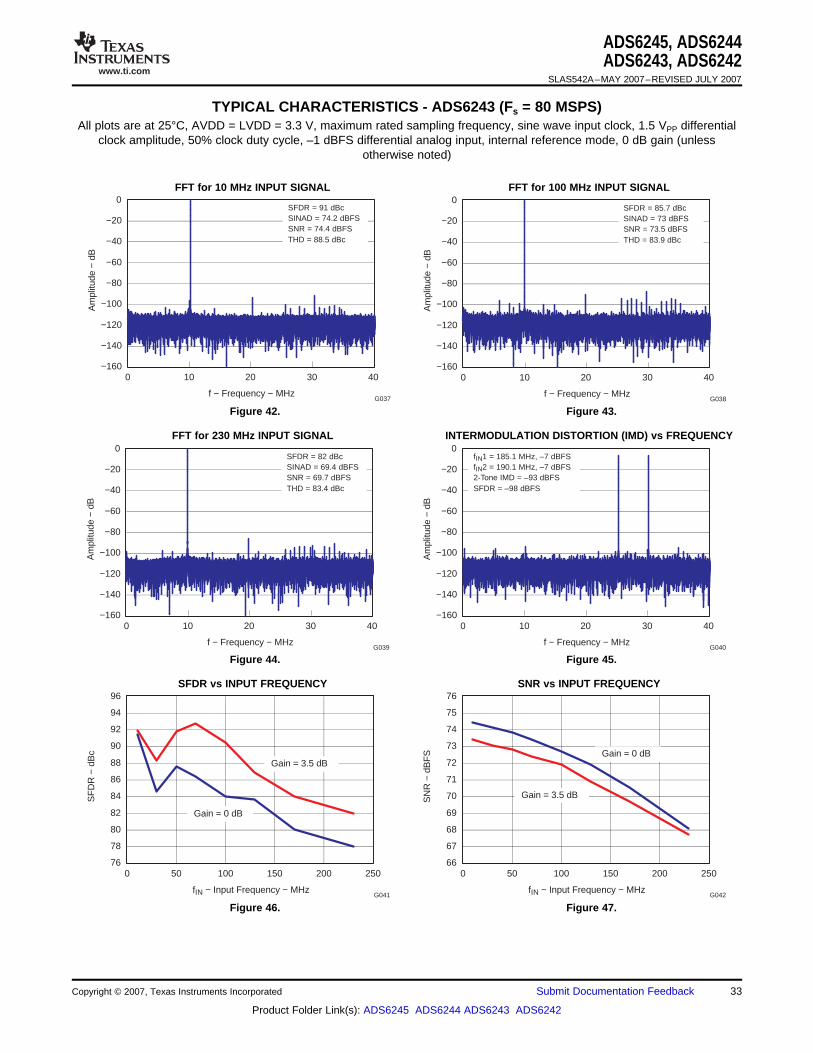
TYPICAL CHARACTERISTICS - ADS6243 (Fs = 80 MSPS)
f − Frequency − MHz
−160
−140
−120
−100
−80
−60
−40
−20
0
0 10 20 30 40
Am
plitu
de −
dB
G037
SFDR = 91 dBcSINAD = 74.2 dBFSSNR = 74.4 dBFSTHD = 88.5 dBc
f − Frequency − MHz
−160
−140
−120
−100
−80
−60
−40
−20
0
0 10 20 30 40
Am
plitu
de −
dB
G038
SFDR = 85.7 dBcSINAD = 73 dBFSSNR = 73.5 dBFSTHD = 83.9 dBc
f − Frequency − MHz
−160
−140
−120
−100
−80
−60
−40
−20
0
0 10 20 30 40
Am
plitu
de −
dB
G039
SFDR = 82 dBcSINAD = 69.4 dBFSSNR = 69.7 dBFSTHD = 83.4 dBc
f − Frequency − MHz
−160
−140
−120
−100
−80
−60
−40
−20
0
0 10 20 30 40
Am
plitu
de −
dB
G040
fIN1 = 185.1 MHz, –7 dBFSfIN2 = 190.1 MHz, –7 dBFS2-Tone IMD = –93 dBFSSFDR = –98 dBFS
fIN − Input Frequency − MHz
76
78
80
82
84
86
88
90
92
94
96
0 50 100 150 200 250
SF
DR
− d
Bc
G041
Gain = 0 dB
Gain = 3.5 dB
fIN − Input Frequency − MHz
66
67
68
69
70
71
72
73
74
75
76
0 50 100 150 200 250
SN
R −
dB
FS
G042
Gain = 0 dB
Gain = 3.5 dB
ADS6245, ADS6244ADS6243, ADS6242
SLAS542A–MAY 2007–REVISED JULY 2007
All plots are at 25°C, AVDD = LVDD = 3.3 V, maximum rated sampling frequency, sine wave input clock, 1.5 VPP differentialclock amplitude, 50% clock duty cycle, –1 dBFS differential analog input, internal reference mode, 0 dB gain (unless
otherwise noted)
FFT for 10 MHz INPUT SIGNAL FFT for 100 MHz INPUT SIGNAL
Figure 42. Figure 43.
FFT for 230 MHz INPUT SIGNAL INTERMODULATION DISTORTION (IMD) vs FREQUENCY
Figure 44. Figure 45.
SFDR vs INPUT FREQUENCY SNR vs INPUT FREQUENCY
Figure 46. Figure 47.
Copyright © 2007, Texas Instruments Incorporated Submit Documentation Feedback 33
Product Folder Link(s): ADS6245 ADS6244 ADS6243 ADS6242
www.ti.com
fIN − Input Frequency − MHz
76
78
80
82
84
86
88
90
92
94
10 30 50 70 90 110 130 150 170 190 210 230
SF
DR
− d
Bc
G043
Input adjusted to get −1dBFS input
1 dB
6 dB2 dB
4 dB
3 dB5 dB
0 dB
fIN − Input Frequency − MHz
65
66
67
68
69
70
71
72
73
74
75
20 40 60 80 100 120 140 160 180 200 220
SIN
AD
− d
BF
S
G044
2 dB
5 dB
1 dB
0 dB
3 dB 3.5 dB
4 dB
6 dB
SN
R −
dB
FS
72
73
74
75
76
77
78
AVDD − Supply Voltage − V
82
84
86
88
90
92
94
3.0 3.1 3.2 3.3 3.4 3.5 3.6
SF
DR
− d
Bc
G045
SNR
SFDR
fIN = 50.1 MHzLVDD = 3.3 V
SN
R −
dB
FS
70
71
72
73
74
75
76
LVDD − Supply Voltage − V
86
87
88
89
90
91
92
3.0 3.1 3.2 3.3 3.4 3.5 3.6
SF
DR
− d
Bc
G046
fIN = 50.1 MHzAVDD = 3.3 V
SNR
SFDR
50
55
60
65
70
75
80
85
90
Input Amplitude − dBFS
30
40
50
60
70
80
90
100
110
−60 −50 −40 −30 −20 −10 0
fIN = 20 MHz
SF
DR
− d
Bc,
dB
FS
G048
SN
R −
dB
FS
SFDR (dBc)
SFDR (dBFS)
SNR (dBFS)
SN
R −
dB
FS
73
74
75
76
77
78
T − Temperature − °C
82
84
86
88
90
92
−40 −20 0 20 40 60 80
SF
DR
− d
Bc
G047
fIN = 50.1 MHz
SNR
SFDR
ADS6245, ADS6244ADS6243, ADS6242SLAS542A–MAY 2007–REVISED JULY 2007
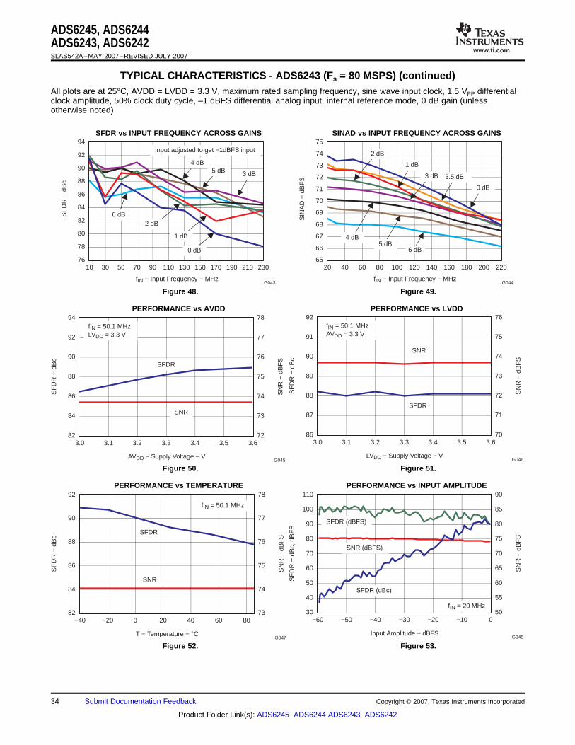
TYPICAL CHARACTERISTICS - ADS6243 (Fs = 80 MSPS) (continued)All plots are at 25°C, AVDD = LVDD = 3.3 V, maximum rated sampling frequency, sine wave input clock, 1.5 VPP differentialclock amplitude, 50% clock duty cycle, –1 dBFS differential analog input, internal reference mode, 0 dB gain (unlessotherwise noted)
SFDR vs INPUT FREQUENCY ACROSS GAINS SINAD vs INPUT FREQUENCY ACROSS GAINS
Figure 48. Figure 49.
PERFORMANCE vs AVDD PERFORMANCE vs LVDD
Figure 50. Figure 51.
PERFORMANCE vs TEMPERATURE PERFORMANCE vs INPUT AMPLITUDE
Figure 52. Figure 53.
34 Submit Documentation Feedback Copyright © 2007, Texas Instruments Incorporated
Product Folder Link(s): ADS6245 ADS6244 ADS6243 ADS6242

www.ti.com
SN
R −
dB
FS
70
71
72
73
74
75
76
77
78
76
78
80
82
84
86
88
90
92
0.5 1.0 1.5 2.0 2.5 3.0
SF
DR
− d
Bc
Input Clock Amplitude − VPP G049
SNR
SFDR
fIN = 50.1 MHz
SN
R −
dB
FS
71
72
73
74
75
76
Input Clock Duty Cycle − %
82
84
86
88
90
92
35 40 45 50 55 60 65
SF
DR
− d
Bc
G050
SNR
SFDR
fIN = 20.1 MHz
fS − Sampling Frequency − MSPS
0.0
0.1
0.2
0.3
0.4
0.5
0.6
0.7
0.8
0.9
1.0
0 20 40 60 80
PD
− P
ower
Dis
sipa
tion
− W
G051
LVDD
AVDD
Output Code
0
5
10
15
20
25
30
35
40
8180 8181 8182 8183 8184 8185 8186 8187 8188 8189
Occ
uren
ce −
%
G052
RMS (LSB) = 1.016
f − Frequency − MHz
−100
−90
−80
−70
−60
−50
−40
−30
−20
−10
0
0 50 100 150 200 250 300
CM
RR
− C
omm
on-M
ode
Rej
ectio
n R
atio
− d
Bc
G018
SN
R −
dB
FS
66
68
70
72
74
76
VVCM − VCM Voltage − V
86
88
90
92
94
96
1.30 1.35 1.40 1.45 1.50 1.55 1.60 1.65 1.70
fIN = 50.1 MHzExternal Reference Mode
SF
DR
− d
Bc
G053
SNR
SFDR
ADS6245, ADS6244ADS6243, ADS6242
SLAS542A–MAY 2007–REVISED JULY 2007
TYPICAL CHARACTERISTICS - ADS6243 (Fs = 80 MSPS) (continued)All plots are at 25°C, AVDD = LVDD = 3.3 V, maximum rated sampling frequency, sine wave input clock, 1.5 VPP differentialclock amplitude, 50% clock duty cycle, –1 dBFS differential analog input, internal reference mode, 0 dB gain (unlessotherwise noted)
PERFORMANCE vs CLOCK AMPLITUDE PERFORMANCE vs CLOCK DUTY CYCLE
Figure 54. Figure 55.
OUTPUT NOISE HISTOGRAM WITHPOWER DISSIPATION vs SAMPLING FREQUENCY INPUTS TIED TO COMMON-MODE
Figure 56. Figure 57.
PERFORMANCE IN EXTERNAL REFERENCE MODE CMRR vs FREQUENCY
Figure 58. Figure 59.
Copyright © 2007, Texas Instruments Incorporated Submit Documentation Feedback 35
Product Folder Link(s): ADS6245 ADS6244 ADS6243 ADS6242
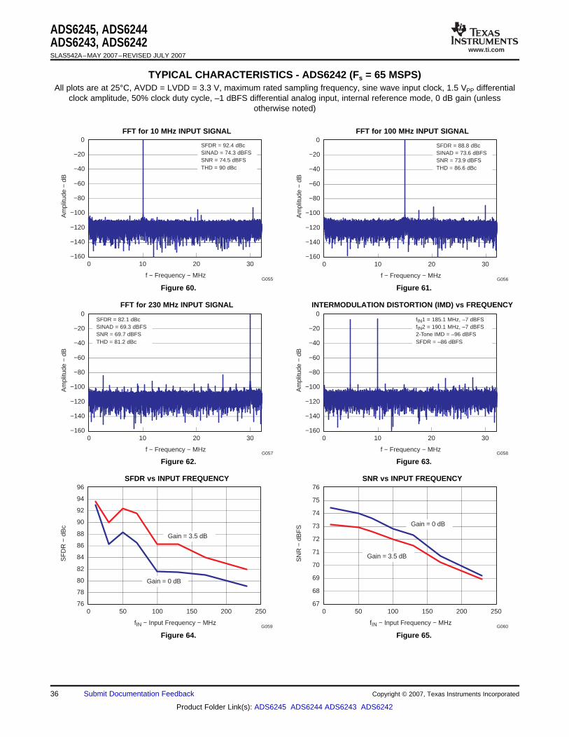
www.ti.com
TYPICAL CHARACTERISTICS - ADS6242 (Fs = 65 MSPS)
f − Frequency − MHz
−160
−140
−120
−100
−80
−60
−40
−20
0
0 10 20 30
Am
plitu
de −
dB
G055
SFDR = 92.4 dBcSINAD = 74.3 dBFSSNR = 74.5 dBFSTHD = 90 dBc
f − Frequency − MHz
−160
−140
−120
−100
−80
−60
−40
−20
0
0 10 20 30
Am
plitu
de −
dB
G056
SFDR = 88.8 dBcSINAD = 73.6 dBFSSNR = 73.9 dBFSTHD = 86.6 dBc
f − Frequency − MHz
−160
−140
−120
−100
−80
−60
−40
−20
0
0 10 20 30
Am
plitu
de −
dB
G057
SFDR = 82.1 dBcSINAD = 69.3 dBFSSNR = 69.7 dBFSTHD = 81.2 dBc
f − Frequency − MHz
−160
−140
−120
−100
−80
−60
−40
−20
0
0 10 20 30
Am
plitu
de −
dB
G058
fIN1 = 185.1 MHz, –7 dBFSfIN2 = 190.1 MHz, –7 dBFS2-Tone IMD = –96 dBFSSFDR = –86 dBFS
fIN − Input Frequency − MHz
76
78
80
82
84
86
88
90
92
94
96
0 50 100 150 200 250
SF
DR
− d
Bc
G059
Gain = 0 dB
Gain = 3.5 dB
fIN − Input Frequency − MHz
67
68
69
70
71
72
73
74
75
76
0 50 100 150 200 250
SN
R −
dB
FS
G060
Gain = 0 dB
Gain = 3.5 dB
ADS6245, ADS6244ADS6243, ADS6242SLAS542A–MAY 2007–REVISED JULY 2007
All plots are at 25°C, AVDD = LVDD = 3.3 V, maximum rated sampling frequency, sine wave input clock, 1.5 VPP differentialclock amplitude, 50% clock duty cycle, –1 dBFS differential analog input, internal reference mode, 0 dB gain (unless
otherwise noted)
FFT for 10 MHz INPUT SIGNAL FFT for 100 MHz INPUT SIGNAL
Figure 60. Figure 61.
FFT for 230 MHz INPUT SIGNAL INTERMODULATION DISTORTION (IMD) vs FREQUENCY
Figure 62. Figure 63.
SFDR vs INPUT FREQUENCY SNR vs INPUT FREQUENCY
Figure 64. Figure 65.
36 Submit Documentation Feedback Copyright © 2007, Texas Instruments Incorporated
Product Folder Link(s): ADS6245 ADS6244 ADS6243 ADS6242

www.ti.com
fIN − Input Frequency − MHz
76
78
80
82
84
86
88
90
92
94
96
10 30 50 70 90 110 130 150 170 190 210 230
SF
DR
− d
Bc
G061
Input adjusted to get −1dBFS input
6 dB
2 dB
4 dB3 dB
5 dB
0 dB
1 dB
fIN − Input Frequency − MHz
65
66
67
68
69
70
71
72
73
74
75
20 40 60 80 100 120 140 160 180 200 220
SIN
AD
− d
BF
S
G062
2 dB
5 dB
1 dB
0 dB3 dB
3.5 dB
4 dB6 dB
SN
R −
dB
FS
72
73
74
75
76
77
78
AVDD − Supply Voltage − V
82
84
86
88
90
92
94
3.0 3.1 3.2 3.3 3.4 3.5 3.6
SF
DR
− d
Bc
G063
SNR
SFDR
fIN = 50.1 MHzLVDD = 3.3 V
SN
R −
dB
FS
70
71
72
73
74
75
76
LVDD − Supply Voltage − V
86
87
88
89
90
91
92
3.0 3.1 3.2 3.3 3.4 3.5 3.6
SF
DR
− d
Bc
G064
fIN = 50.1 MHzAVDD = 3.3 V
SNR
SFDR
SN
R −
dB
FS
73
74
75
76
77
78
79
T − Temperature − °C
84
86
88
90
92
94
96
−40 −20 0 20 40 60 80
SF
DR
− d
Bc
G065
fIN = 50.1 MHz
SNR
SFDR
50
55
60
65
70
75
80
85
90
Input Amplitude − dBFS
30
40
50
60
70
80
90
100
110
−60 −50 −40 −30 −20 −10 0
fIN = 20 MHz
SF
DR
− d
Bc,
dB
FS
G066
SN
R −
dB
FS
SFDR (dBc)
SFDR (dBFS)
SNR (dBFS)
ADS6245, ADS6244ADS6243, ADS6242
SLAS542A–MAY 2007–REVISED JULY 2007
TYPICAL CHARACTERISTICS - ADS6242 (Fs = 65 MSPS) (continued)All plots are at 25°C, AVDD = LVDD = 3.3 V, maximum rated sampling frequency, sine wave input clock, 1.5 VPP differentialclock amplitude, 50% clock duty cycle, –1 dBFS differential analog input, internal reference mode, 0 dB gain (unlessotherwise noted)
SFDR vs INPUT FREQUENCY ACROSS GAINS SINAD vs INPUT FREQUENCY ACROSS GAINS
Figure 66. Figure 67.
PERFORMANCE vs AVDD PERFORMANCE vs LVDD
Figure 68. Figure 69.
PERFORMANCE vs TEMPERATURE PERFORMANCE vs INPUT AMPLITUDE
Figure 70. Figure 71.
Copyright © 2007, Texas Instruments Incorporated Submit Documentation Feedback 37
Product Folder Link(s): ADS6245 ADS6244 ADS6243 ADS6242

www.ti.com
SN
R −
dB
FS
71
72
73
74
75
76
Input Clock Duty Cycle − %
85
87
89
91
93
95
35 40 45 50 55 60 65
SF
DR
− d
Bc
G068
SNR
SFDR
fIN = 20.1 MHz
SN
R −
dB
FS
72
73
74
75
76
77
78
79
80
80
82
84
86
88
90
92
94
96
0.5 1.0 1.5 2.0 2.5 3.0
SF
DR
− d
Bc
Input Clock Amplitude − VPP G067
SNR
SFDR
fIN = 50.1 MHz
fS − Sampling Frequency − MSPS
0.0
0.1
0.2
0.3
0.4
0.5
0.6
0.7
0.8
0.9
1.0
0 10 20 30 40 50 60
PD
− P
ower
Dis
sipa
tion
− W
G069
LVDD
AVDD
Output Code
0
5
10
15
20
25
30
35
40
8189 8190 8191 8192 8193 8194 8195 8196 8197
Occ
uren
ce −
%
G070
RMS (LSB) = 1.027
f − Frequency − MHz
−100
−90
−80
−70
−60
−50
−40
−30
−20
−10
0
0 50 100 150 200 250 300
CM
RR
− C
omm
on-M
ode
Rej
ectio
n R
atio
− d
Bc
G018
SN
R −
dB
FS
66
68
70
72
74
76
VVCM − VCM Voltage − V
86
88
90
92
94
96
1.30 1.35 1.40 1.45 1.50 1.55 1.60 1.65 1.70
fIN = 50.1 MHzExternal Reference Mode
SF
DR
− d
Bc
G071
SNR
SFDR
ADS6245, ADS6244ADS6243, ADS6242SLAS542A–MAY 2007–REVISED JULY 2007
TYPICAL CHARACTERISTICS - ADS6242 (Fs = 65 MSPS) (continued)All plots are at 25°C, AVDD = LVDD = 3.3 V, maximum rated sampling frequency, sine wave input clock, 1.5 VPP differentialclock amplitude, 50% clock duty cycle, –1 dBFS differential analog input, internal reference mode, 0 dB gain (unlessotherwise noted)
PERFORMANCE vs CLOCK AMPLITUDE PERFORMANCE vs CLOCK DUTY CYCLE
Figure 72. Figure 73.
OUTPUT NOISE HISTOGRAM WITHPOWER DISSIPATION vs SAMPLING FREQUENCY INPUTS TIED TO COMMON-MODE
Figure 74. Figure 75.
PERFORMANCE IN EXTERNAL REFERENCE MODE CMRR vs FREQUENCY
Figure 76. Figure 77.
38 Submit Documentation Feedback Copyright © 2007, Texas Instruments Incorporated
Product Folder Link(s): ADS6245 ADS6244 ADS6243 ADS6242

www.ti.com
Contour Plots across Input and Sampling Frequencies
10 50 100 150
f - Input Frequency - MHzIN
f-
Sam
plin
g F
req
uen
cy -
MS
PS
S
SFDR - dBc
200 250 300 400 450350 50030
40
50
100
60
70
80
90
110
120
125
65 70 8075 85 90
M0049-13
8383
83
86
86
86
86
83
80
80
80
80
77
77
77
74
74
74 71
71
71
68
68
68
65
65
65
86
83
83
89
89
89
89
92
8086
10 50 100 150
f - Input Frequency - MHzIN
f-
Sam
plin
g F
req
uen
cy -
MS
PS
S
SFDR - dBc
200 250 300 400 450350 50030
40
50
100
60
70
80
90
110
120
125
65 70 8075 85 90
M0049-14
88
85
88
88
88
85
82
82
82
79
82
91
79
79
7976
76
76
76
73
73
73
70
70
70
67
94
91
91
88
85
85
91
ADS6245, ADS6244ADS6243, ADS6242
SLAS542A–MAY 2007–REVISED JULY 2007
Figure 78. SFDR Contour (no gain)
Figure 79. SFDR Contour (3.5 dB coarse gain)
Copyright © 2007, Texas Instruments Incorporated Submit Documentation Feedback 39
Product Folder Link(s): ADS6245 ADS6244 ADS6243 ADS6242
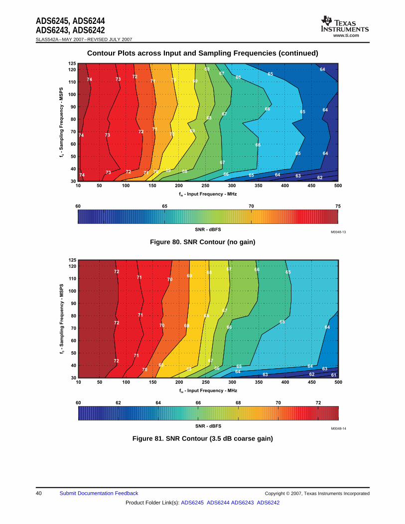
www.ti.com
10 50 100 150
f - Input Frequency - MHzIN
f-
Sam
plin
g F
req
uen
cy -
MS
PS
S
SNR - dBFS
200 250 300 400 450350 50030
40
50
100
60
70
80
90
110
120
125
60 65 7570
M0048-13
73
73
73
71
71
71
72
72
72
70
70
70
69
69
69
68
68
68
67
67
67
66
66
66
66
65
65
65
65
64
64
64
64 63 62
74
74
74
10 50 100 150
f - Input Frequency - MHzIN
f-
Sam
plin
g F
req
uen
cy -
MS
PS
S
SNR - dBFS
200 250 300 400 450350 50030
40
50
100
60
70
80
90
110
120
125
60 6462 66 68 70 72
M0048-14
71
71
71
72
72
72
70
70
70
69
69
69
68
68
68
67
67
67
66
66
66
65
65
65
64
64
6463
63
62 61
ADS6245, ADS6244ADS6243, ADS6242SLAS542A–MAY 2007–REVISED JULY 2007
Contour Plots across Input and Sampling Frequencies (continued)
Figure 80. SNR Contour (no gain)
Figure 81. SNR Contour (3.5 dB coarse gain)
40 Submit Documentation Feedback Copyright © 2007, Texas Instruments Incorporated
Product Folder Link(s): ADS6245 ADS6244 ADS6243 ADS6242
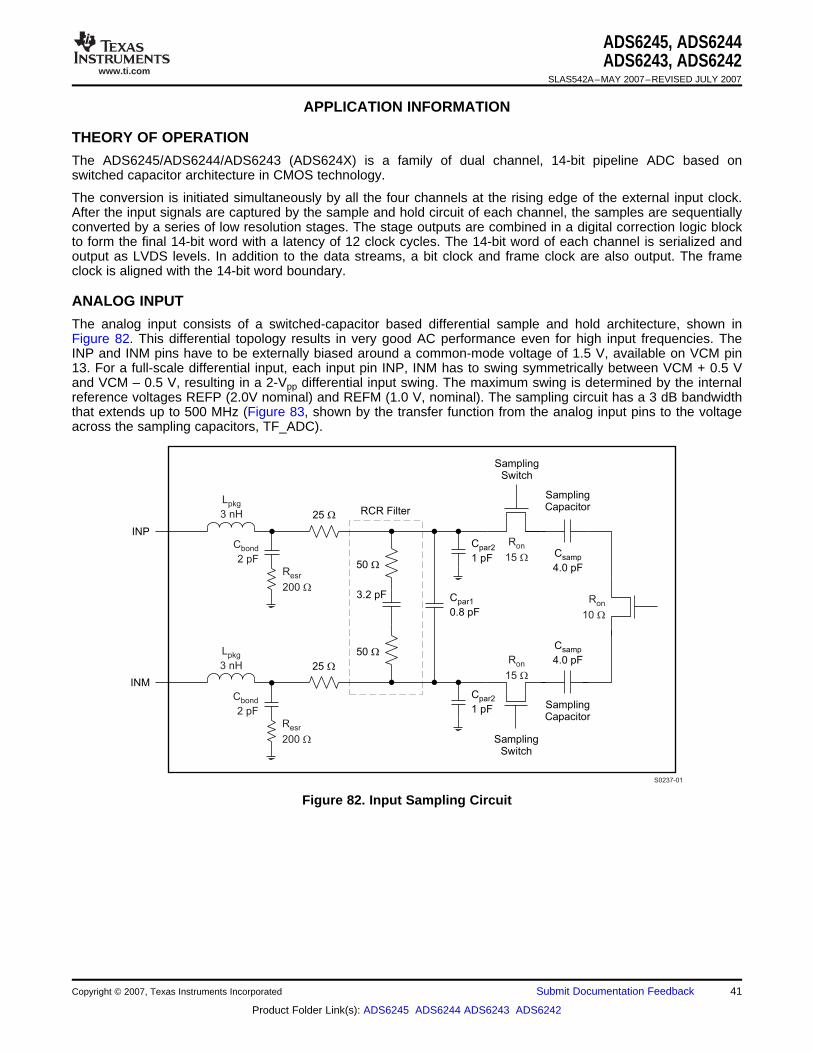
www.ti.com
APPLICATION INFORMATION
THEORY OF OPERATION
ANALOG INPUT
INP
INM
25 W
25 W
RCR Filter
50 W
50 W
3.2 pF
C
1 pFpar2
C
1 pFpar2
L
3 nHpkg
L
3 nHpkg
C
2 pFbond
C
2 pFbond
R
200esr
W
R
200esr
W
C
0.8 pFpar1
SamplingSwitch
SamplingSwitch
SamplingCapacitor
SamplingCapacitor
R
15on
W
R
15on
W
R
10on
W
C
4.0 pFsamp
C
4.0 pFsamp
S0237-01
ADS6245, ADS6244ADS6243, ADS6242
SLAS542A–MAY 2007–REVISED JULY 2007
The ADS6245/ADS6244/ADS6243 (ADS624X) is a family of dual channel, 14-bit pipeline ADC based onswitched capacitor architecture in CMOS technology.
The conversion is initiated simultaneously by all the four channels at the rising edge of the external input clock.After the input signals are captured by the sample and hold circuit of each channel, the samples are sequentiallyconverted by a series of low resolution stages. The stage outputs are combined in a digital correction logic blockto form the final 14-bit word with a latency of 12 clock cycles. The 14-bit word of each channel is serialized andoutput as LVDS levels. In addition to the data streams, a bit clock and frame clock are also output. The frameclock is aligned with the 14-bit word boundary.
The analog input consists of a switched-capacitor based differential sample and hold architecture, shown inFigure 82. This differential topology results in very good AC performance even for high input frequencies. TheINP and INM pins have to be externally biased around a common-mode voltage of 1.5 V, available on VCM pin13. For a full-scale differential input, each input pin INP, INM has to swing symmetrically between VCM + 0.5 Vand VCM – 0.5 V, resulting in a 2-Vpp differential input swing. The maximum swing is determined by the internalreference voltages REFP (2.0V nominal) and REFM (1.0 V, nominal). The sampling circuit has a 3 dB bandwidththat extends up to 500 MHz (Figure 83, shown by the transfer function from the analog input pins to the voltageacross the sampling capacitors, TF_ADC).
Figure 82. Input Sampling Circuit
Copyright © 2007, Texas Instruments Incorporated Submit Documentation Feedback 41
Product Folder Link(s): ADS6245 ADS6244 ADS6243 ADS6242
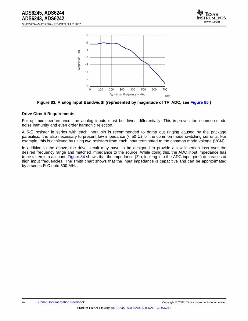
www.ti.com
fIN − Input Frequency − MHz
−6
−5
−4
−3
−2
−1
0
1
0 100 200 300 400 500 600 700
Mag
nitu
de −
dB
G073
Drive Circuit Requirements
ADS6245, ADS6244ADS6243, ADS6242SLAS542A–MAY 2007–REVISED JULY 2007
Figure 83. Analog Input Bandwidth (represented by magnitude of TF_ADC, see Figure 85 )
For optimum performance, the analog inputs must be driven differentially. This improves the common-modenoise immunity and even order harmonic rejection.
A 5-Ω resistor in series with each input pin is recommended to damp out ringing caused by the packageparasitics. It is also necessary to present low impedance (< 50 Ω) for the common mode switching currents. Forexample, this is achieved by using two resistors from each input terminated to the common mode voltage (VCM).
In addition to the above, the drive circuit may have to be designed to provide a low insertion loss over thedesired frequency range and matched impedance to the source. While doing this, the ADC input impedance hasto be taken into account. Figure 84 shows that the impedance (Zin, looking into the ADC input pins) decreases athigh input frequencies. The smith chart shows that the input impedance is capacitive and can be approximatedby a series R-C upto 500 MHz.
42 Submit Documentation Feedback Copyright © 2007, Texas Instruments Incorporated
Product Folder Link(s): ADS6245 ADS6244 ADS6243 ADS6242
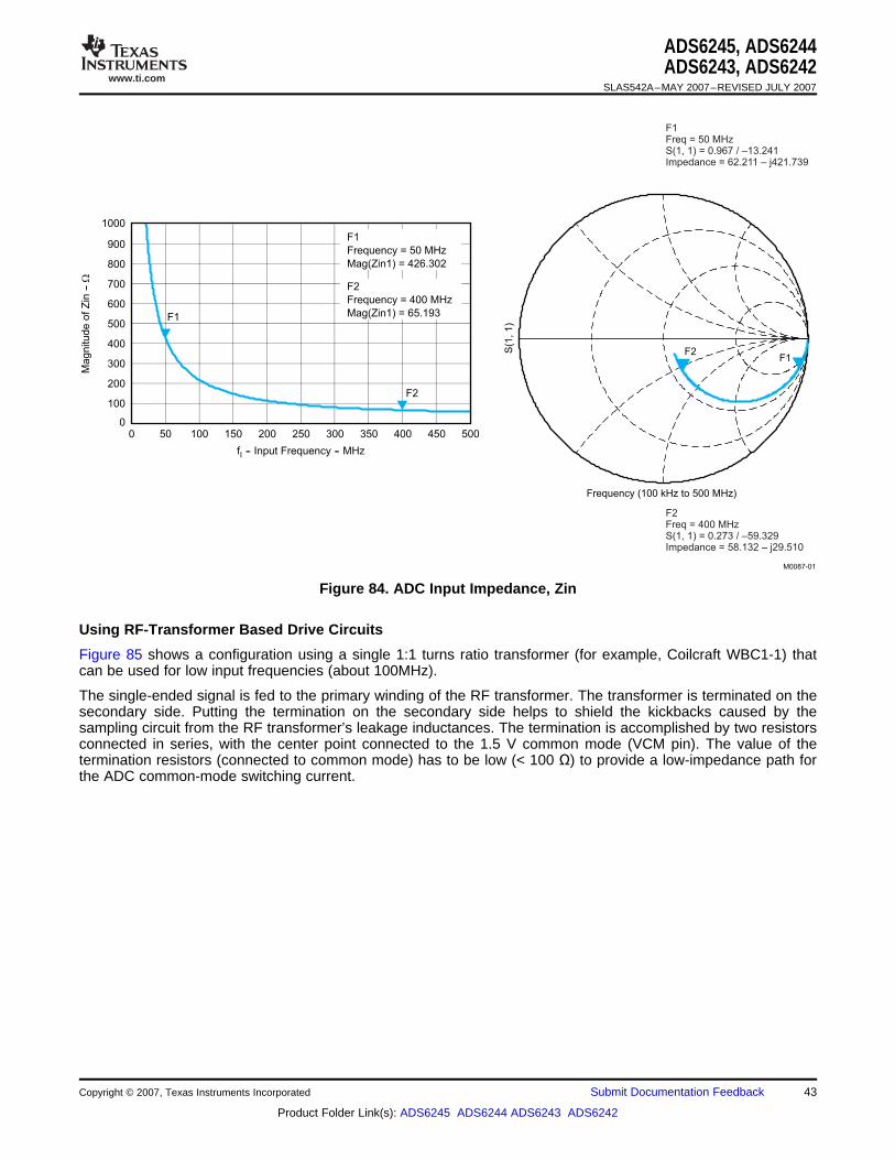
www.ti.com
M0087-01
S(1
, 1
)
Frequency (100 kHz to 500 MHz)
F2F1
F1Freq = 50 MHzS(1, 1) = 0.967 / –13.241Impedance = 62.211 – j421.739
F2Freq = 400 MHzS(1, 1) = 0.273 / –59.329Impedance = 58.132 – j29.510
0
100
200
300
400
500
600
700
800
900
1000
0 50 100 150 200 250 300 350 400 450 500
Ma
gn
itu
de
of
Zin
--W
f -- Input Frequency -- MHzI
F1
F1
Frequency = 50 MHz
Mag(Zin1) = 426.302
F2
F2
Frequency = 400 MHz
Mag(Zin1) = 65.193
Using RF-Transformer Based Drive Circuits
ADS6245, ADS6244ADS6243, ADS6242
SLAS542A–MAY 2007–REVISED JULY 2007
Figure 84. ADC Input Impedance, Zin
Figure 85 shows a configuration using a single 1:1 turns ratio transformer (for example, Coilcraft WBC1-1) thatcan be used for low input frequencies (about 100MHz).
The single-ended signal is fed to the primary winding of the RF transformer. The transformer is terminated on thesecondary side. Putting the termination on the secondary side helps to shield the kickbacks caused by thesampling circuit from the RF transformer’s leakage inductances. The termination is accomplished by two resistorsconnected in series, with the center point connected to the 1.5 V common mode (VCM pin). The value of thetermination resistors (connected to common mode) has to be low (< 100 Ω) to provide a low-impedance path forthe ADC common-mode switching current.
Copyright © 2007, Texas Instruments Incorporated Submit Documentation Feedback 43
Product Folder Link(s): ADS6245 ADS6244 ADS6243 ADS6242
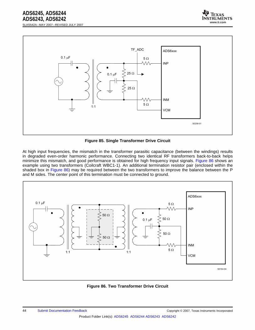
www.ti.com
INP
INM
VCM1:1
5 W
25 W
25 W
5 W
0.1 Fm
0.1 Fm
TF_ADC
S0256-01
ADS6xxx
INP
INM
VCM
1:1 1:1
5 W
50 W50 W
50 W
50 W
5 W
0.1 Fm
0.1 Fm
S0164-04
ADS6xxx
ADS6245, ADS6244ADS6243, ADS6242SLAS542A–MAY 2007–REVISED JULY 2007
Figure 85. Single Transformer Drive Circuit
At high input frequencies, the mismatch in the transformer parasitic capacitance (between the windings) resultsin degraded even-order harmonic performance. Connecting two identical RF transformers back-to-back helpsminimize this mismatch, and good performance is obtained for high frequency input signals. Figure 86 shows anexample using two transformers (Coilcraft WBC1-1). An additional termination resistor pair (enclosed within theshaded box in Figure 86) may be required between the two transformers to improve the balance between the Pand M sides. The center point of this termination must be connected to ground.
Figure 86. Two Transformer Drive Circuit
44 Submit Documentation Feedback Copyright © 2007, Texas Instruments Incorporated
Product Folder Link(s): ADS6245 ADS6244 ADS6243 ADS6242
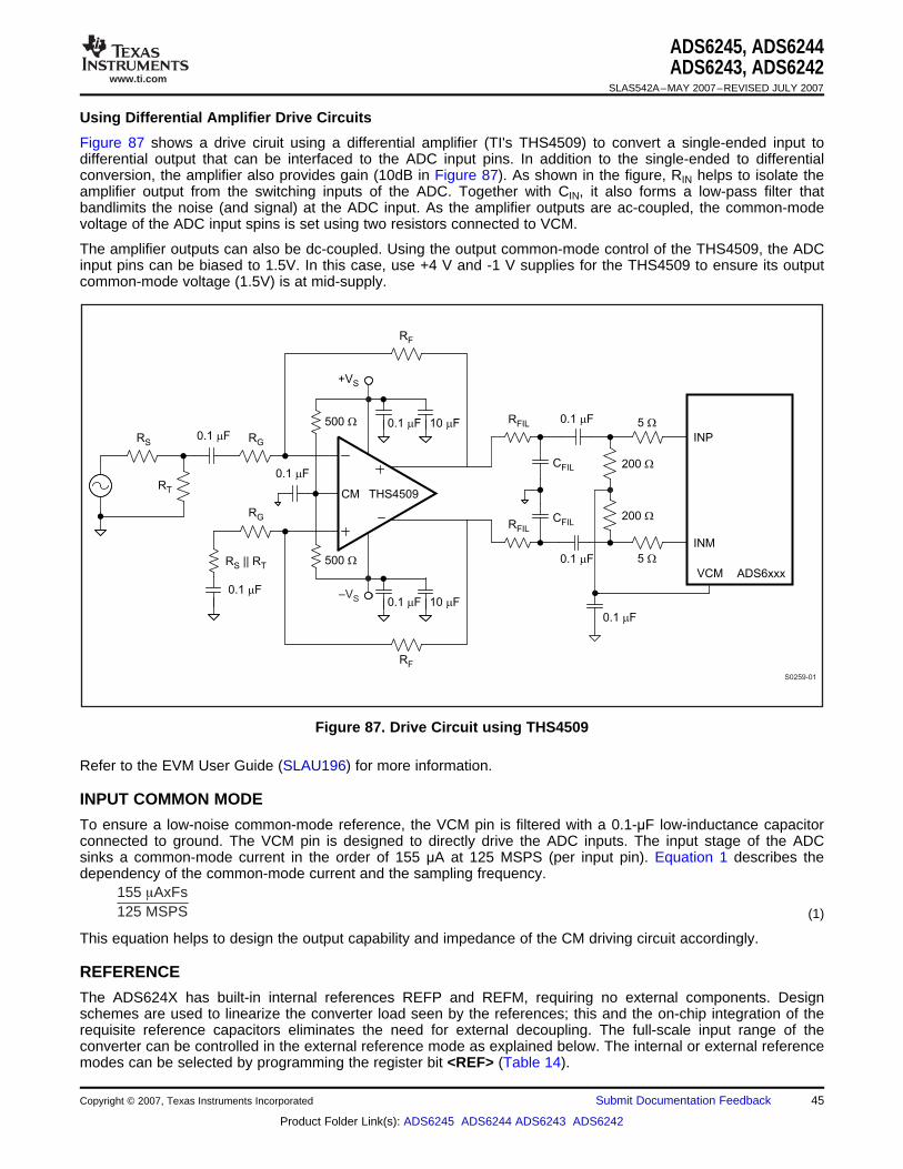
www.ti.com
Using Differential Amplifier Drive Circuits
RG
RF
RF
RFIL
RFIL
CFIL
CFILRG
0.1 Fm
0.1 Fm
0.1 Fm
0.1 Fm
0.1 Fm
0.1 Fm
0.1 Fm
10 Fm
10 Fm
RS
RS T|| R
RT
+VS
CM
INP
INM
ADS6xxx
THS4509
VCM
500 W
200 W
200 W
5 W
5 W500 W
0.1 Fm
–VS
S0259-01
INPUT COMMON MODE
155 AxFs125 MSPS (1)
REFERENCE
ADS6245, ADS6244ADS6243, ADS6242
SLAS542A–MAY 2007–REVISED JULY 2007
Figure 87 shows a drive ciruit using a differential amplifier (TI's THS4509) to convert a single-ended input todifferential output that can be interfaced to the ADC input pins. In addition to the single-ended to differentialconversion, the amplifier also provides gain (10dB in Figure 87). As shown in the figure, RIN helps to isolate theamplifier output from the switching inputs of the ADC. Together with CIN, it also forms a low-pass filter thatbandlimits the noise (and signal) at the ADC input. As the amplifier outputs are ac-coupled, the common-modevoltage of the ADC input spins is set using two resistors connected to VCM.
The amplifier outputs can also be dc-coupled. Using the output common-mode control of the THS4509, the ADCinput pins can be biased to 1.5V. In this case, use +4 V and -1 V supplies for the THS4509 to ensure its outputcommon-mode voltage (1.5V) is at mid-supply.
Figure 87. Drive Circuit using THS4509
Refer to the EVM User Guide (SLAU196) for more information.
To ensure a low-noise common-mode reference, the VCM pin is filtered with a 0.1-μF low-inductance capacitorconnected to ground. The VCM pin is designed to directly drive the ADC inputs. The input stage of the ADCsinks a common-mode current in the order of 155 μA at 125 MSPS (per input pin). Equation 1 describes thedependency of the common-mode current and the sampling frequency.
This equation helps to design the output capability and impedance of the CM driving circuit accordingly.
The ADS624X has built-in internal references REFP and REFM, requiring no external components. Designschemes are used to linearize the converter load seen by the references; this and the on-chip integration of therequisite reference capacitors eliminates the need for external decoupling. The full-scale input range of theconverter can be controlled in the external reference mode as explained below. The internal or external referencemodes can be selected by programming the register bit <REF> (Table 14).
Copyright © 2007, Texas Instruments Incorporated Submit Documentation Feedback 45
Product Folder Link(s): ADS6245 ADS6244 ADS6243 ADS6242
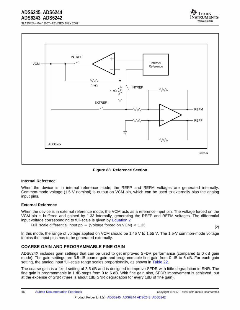
www.ti.com
S0165-04
VCM
REFM
REFP
INTREF
INTREF
EXTREF
4 kW
1 kW
Internal
Reference
ADS6xxx
Internal Reference
External Reference
Full−scale differential input pp (Voltage forced on VCM) 1.33 (2)
COARSE GAIN AND PROGRAMMABLE FINE GAIN
ADS6245, ADS6244ADS6243, ADS6242SLAS542A–MAY 2007–REVISED JULY 2007
Figure 88. Reference Section
When the device is in internal reference mode, the REFP and REFM voltages are generated internally.Common-mode voltage (1.5 V nominal) is output on VCM pin, which can be used to externally bias the analoginput pins.
When the device is in external reference mode, the VCM acts as a reference input pin. The voltage forced on theVCM pin is buffered and gained by 1.33 internally, generating the REFP and REFM voltages. The differentialinput voltage corresponding to full-scale is given by Equation 2.
In this mode, the range of voltage applied on VCM should be 1.45 V to 1.55 V. The 1.5-V common-mode voltageto bias the input pins has to be generated externally.
ADS624X includes gain settings that can be used to get improved SFDR performance (compared to 0 dB gainmode). The gain settings are 3.5 dB coarse gain and programmable fine gain from 0 dB to 6 dB. For each gainsetting, the analog input full-scale range scales proportionally, as shown in Table 22.
The coarse gain is a fixed setting of 3.5 dB and is designed to improve SFDR with little degradation in SNR. Thefine gain is programmable in 1 dB steps from 0 to 6 dB. With fine gain also, SFDR improvement is achieved, butat the expense of SNR (there is about 1dB SNR degradation for every 1dB of fine gain).
46 Submit Documentation Feedback Copyright © 2007, Texas Instruments Incorporated
Product Folder Link(s): ADS6245 ADS6244 ADS6243 ADS6242
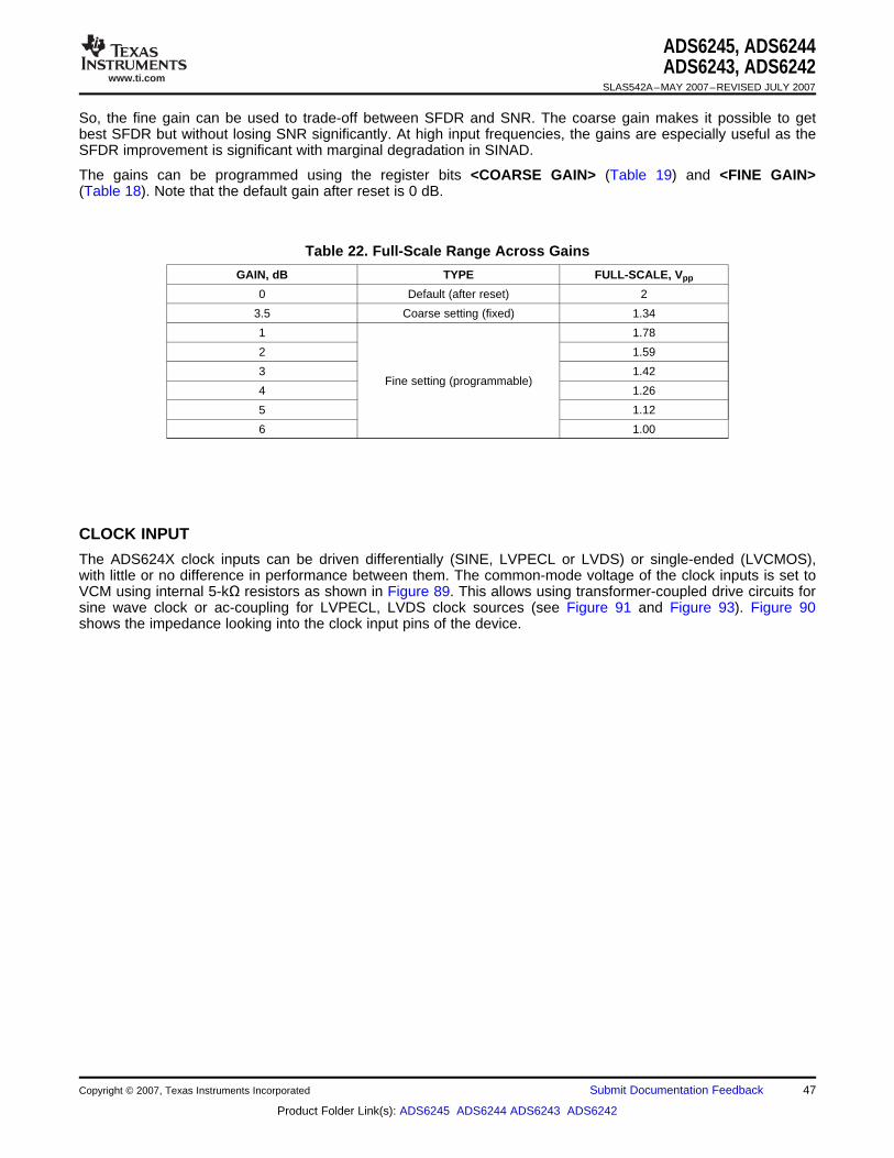
www.ti.com
CLOCK INPUT
ADS6245, ADS6244ADS6243, ADS6242
SLAS542A–MAY 2007–REVISED JULY 2007
So, the fine gain can be used to trade-off between SFDR and SNR. The coarse gain makes it possible to getbest SFDR but without losing SNR significantly. At high input frequencies, the gains are especially useful as theSFDR improvement is significant with marginal degradation in SINAD.
The gains can be programmed using the register bits <COARSE GAIN> (Table 19) and <FINE GAIN>(Table 18). Note that the default gain after reset is 0 dB.
Table 22. Full-Scale Range Across Gains
GAIN, dB TYPE FULL-SCALE, Vpp
0 Default (after reset) 2
3.5 Coarse setting (fixed) 1.34
1 1.78
2 1.59
3 1.42Fine setting (programmable)
4 1.26
5 1.12
6 1.00
The ADS624X clock inputs can be driven differentially (SINE, LVPECL or LVDS) or single-ended (LVCMOS),with little or no difference in performance between them. The common-mode voltage of the clock inputs is set toVCM using internal 5-kΩ resistors as shown in Figure 89. This allows using transformer-coupled drive circuits forsine wave clock or ac-coupling for LVPECL, LVDS clock sources (see Figure 91 and Figure 93). Figure 90shows the impedance looking into the clock input pins of the device.
Copyright © 2007, Texas Instruments Incorporated Submit Documentation Feedback 47
Product Folder Link(s): ADS6245 ADS6244 ADS6243 ADS6242
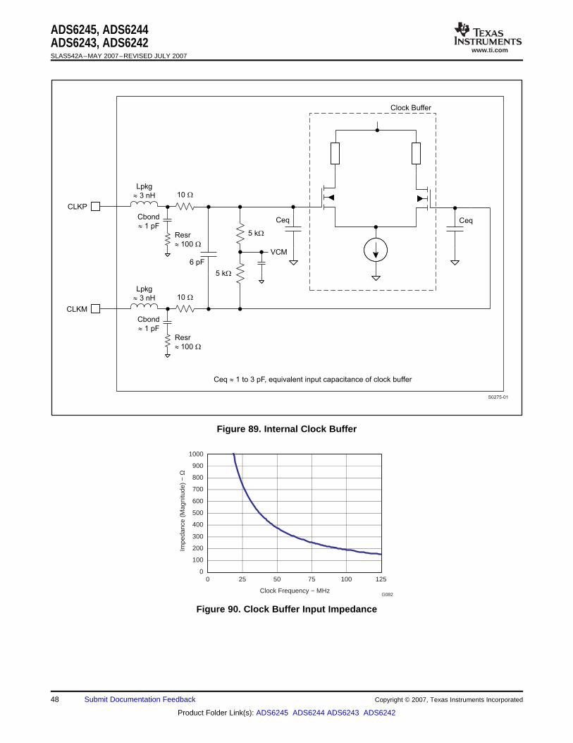
www.ti.com
CLKP
5 kW
VCM
5 kW
6 pF
10 W
10 W
CLKM
Clock Buffer
Ceq Ceq
Ceq 1 to 3 pF, equivalent input capacitance of clock buffer»
Lpkg
3 nH»
Lpkg
3 nH»
Cbond
1 pF»
Cbond
1 pF»
Resr
100» W
Resr
100» W
S0275-01
Clock Frequency − MHz
0
100
200
300
400
500
600
700
800
900
1000
0 25 50 75 100 125
Impe
danc
e (M
agni
tude
) −
Ω
G082
ADS6245, ADS6244ADS6243, ADS6242SLAS542A–MAY 2007–REVISED JULY 2007
Figure 89. Internal Clock Buffer
Figure 90. Clock Buffer Input Impedance
48 Submit Documentation Feedback Copyright © 2007, Texas Instruments Incorporated
Product Folder Link(s): ADS6245 ADS6244 ADS6243 ADS6242
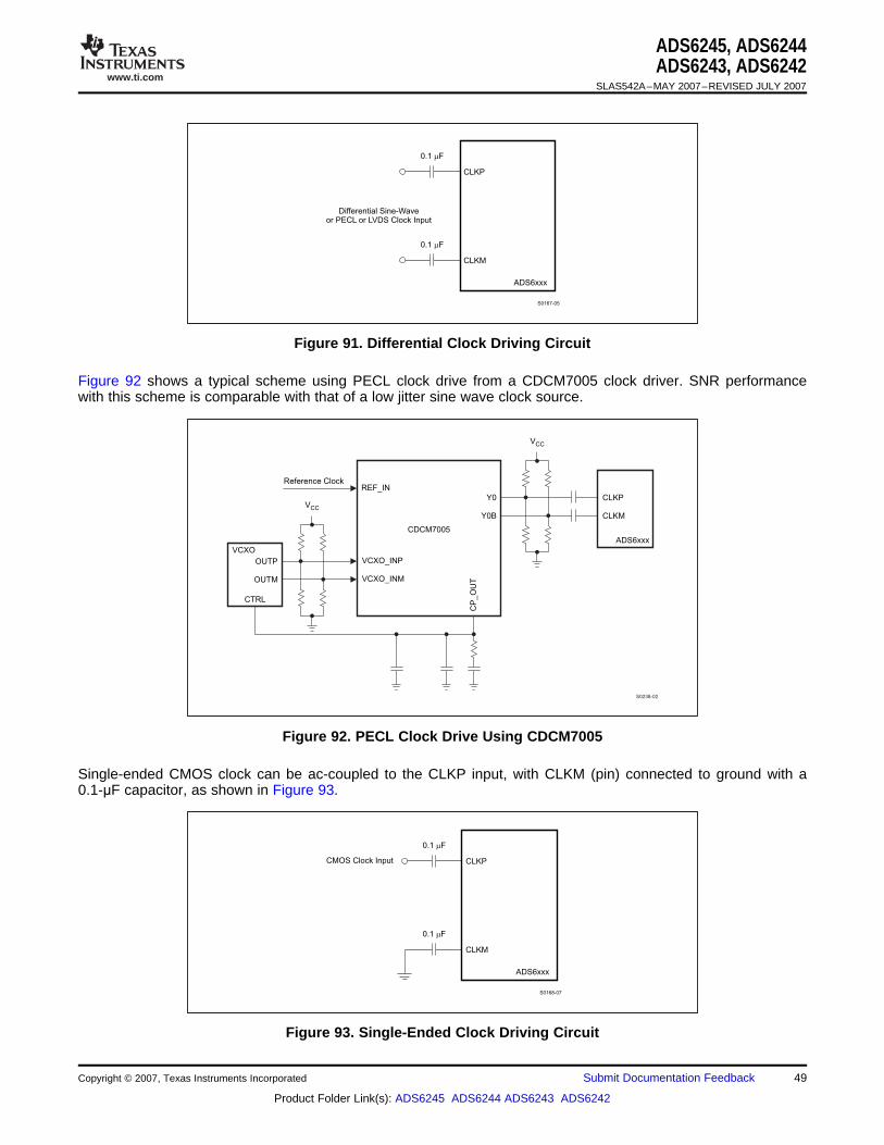
www.ti.com
S0167-05
CLKP
CLKM
Differential Sine-Waveor PECL or LVDS Clock Input
ADS6xxx
0.1 Fm
0.1 Fm
VCC
VCC
REF_IN
VCXO_INM
CP
_O
UT
CTRL
OUTP
OUTM
Y0B
Y0
ADS6xxx
CLKM
CLKP
VCXO
CDCM7005
VCXO_INP
Reference Clock
S0238-02
S0168-07
CLKP
CLKM
CMOS Clock Input
ADS6xxx
0.1 Fm
0.1 Fm
ADS6245, ADS6244ADS6243, ADS6242
SLAS542A–MAY 2007–REVISED JULY 2007
Figure 91. Differential Clock Driving Circuit
Figure 92 shows a typical scheme using PECL clock drive from a CDCM7005 clock driver. SNR performancewith this scheme is comparable with that of a low jitter sine wave clock source.
Figure 92. PECL Clock Drive Using CDCM7005
Single-ended CMOS clock can be ac-coupled to the CLKP input, with CLKM (pin) connected to ground with a0.1-μF capacitor, as shown in Figure 93.
Figure 93. Single-Ended Clock Driving Circuit
Copyright © 2007, Texas Instruments Incorporated Submit Documentation Feedback 49
Product Folder Link(s): ADS6245 ADS6244 ADS6243 ADS6242
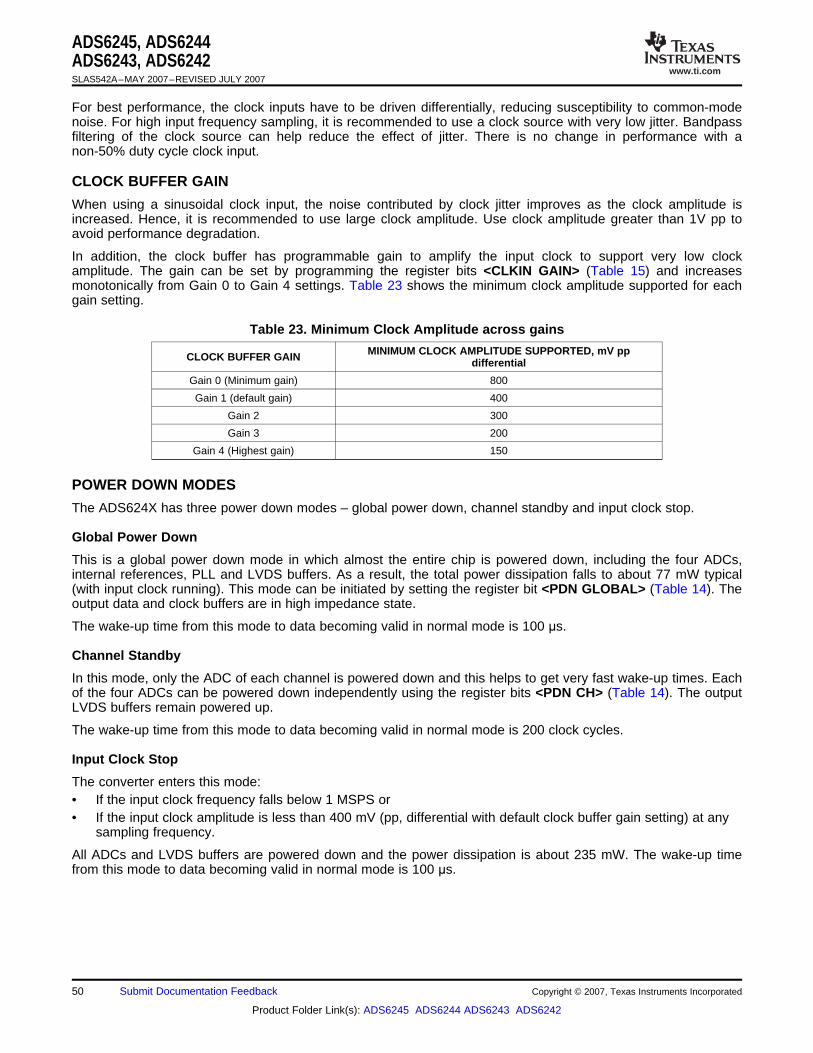
www.ti.com
CLOCK BUFFER GAIN
POWER DOWN MODES
Global Power Down
Channel Standby
Input Clock Stop
ADS6245, ADS6244ADS6243, ADS6242SLAS542A–MAY 2007–REVISED JULY 2007
For best performance, the clock inputs have to be driven differentially, reducing susceptibility to common-modenoise. For high input frequency sampling, it is recommended to use a clock source with very low jitter. Bandpassfiltering of the clock source can help reduce the effect of jitter. There is no change in performance with anon-50% duty cycle clock input.
When using a sinusoidal clock input, the noise contributed by clock jitter improves as the clock amplitude isincreased. Hence, it is recommended to use large clock amplitude. Use clock amplitude greater than 1V pp toavoid performance degradation.
In addition, the clock buffer has programmable gain to amplify the input clock to support very low clockamplitude. The gain can be set by programming the register bits <CLKIN GAIN> (Table 15) and increasesmonotonically from Gain 0 to Gain 4 settings. Table 23 shows the minimum clock amplitude supported for eachgain setting.
Table 23. Minimum Clock Amplitude across gains
MINIMUM CLOCK AMPLITUDE SUPPORTED, mV ppCLOCK BUFFER GAIN differential
Gain 0 (Minimum gain) 800
Gain 1 (default gain) 400
Gain 2 300
Gain 3 200
Gain 4 (Highest gain) 150
The ADS624X has three power down modes – global power down, channel standby and input clock stop.
This is a global power down mode in which almost the entire chip is powered down, including the four ADCs,internal references, PLL and LVDS buffers. As a result, the total power dissipation falls to about 77 mW typical(with input clock running). This mode can be initiated by setting the register bit <PDN GLOBAL> (Table 14). Theoutput data and clock buffers are in high impedance state.
The wake-up time from this mode to data becoming valid in normal mode is 100 μs.
In this mode, only the ADC of each channel is powered down and this helps to get very fast wake-up times. Eachof the four ADCs can be powered down independently using the register bits <PDN CH> (Table 14). The outputLVDS buffers remain powered up.
The wake-up time from this mode to data becoming valid in normal mode is 200 clock cycles.
The converter enters this mode:• If the input clock frequency falls below 1 MSPS or• If the input clock amplitude is less than 400 mV (pp, differential with default clock buffer gain setting) at any
sampling frequency.
All ADCs and LVDS buffers are powered down and the power dissipation is about 235 mW. The wake-up timefrom this mode to data becoming valid in normal mode is 100 μs.
50 Submit Documentation Feedback Copyright © 2007, Texas Instruments Incorporated
Product Folder Link(s): ADS6245 ADS6244 ADS6243 ADS6242

www.ti.com
POWER SUPPLY SEQUENCING
ADS6245, ADS6244ADS6243, ADS6242
SLAS542A–MAY 2007–REVISED JULY 2007
Table 24. Power Down Modes Summary (1)
AVDD POWER LVDD POWERPOWER DOWN MODE WAKE UP TIME(mW) (mW)
In power-up 782 208 –
Global power down 65 12 100 μs
1 Channel in standby 510 208 200 Clocks
2 Channels in standby 235 208 200 Clocks
Input clock stop 200 35 100 μs
(1) Sampling frequency = 125 MSPS.
During power-up, the AVDD and LVDD supplies can come up in any sequence. The two supplies are separatedinside the device. Externally, they can be driven from separate supplies or from a single supply.
Copyright © 2007, Texas Instruments Incorporated Submit Documentation Feedback 51
Product Folder Link(s): ADS6245 ADS6244 ADS6243 ADS6242

www.ti.com
DIGITAL OUTPUT INTERFACE
1-WIRE INTERFACE – 14× AND 16× SERIALIZATION WITH DDR BIT CLOCK
ADS6245, ADS6244ADS6243, ADS6242SLAS542A–MAY 2007–REVISED JULY 2007
The ADS624X offers several flexible output options making it easy to interface to an ASIC or an FPGA. Each ofthese options can be easily programmed using either parallel pins or the serial interface.
The output interface options are:
• 1-wire, 1× frame clock, 14× and 16× serialization with DDR bit clock
• 2-wire, 1× frame clock, 16× serialization, with DDR and SDR bit clock, byte wise/bit wise/word wise
• 2-wire, 1× frame clock, 14× serialization, with SDR bit clock, byte wise/bit wise/word wise
• 2-wire, (0.5 x) frame clock, 14× serialization, with DDR bit clock, byte wise/bit wise/word wise.
The maximum sampling frequency, bit clock frequency and output data rate will vary depending on the interfaceoptions selected (refer to Table 12).
Table 25. Maximum Recommended Sampling Frequency for Different Output Interface Options
MAXIMUMRECOMMENDED BIT CLOCK FRAME CLOCK SERIAL DATA RATE,INTERFACE OPTIONS SAMPLING FREQUENCY, FREQUENCY, MHZ MbpsFREQUENCY, MHZ
MSPS
14× Serialization 65 455 65 910DDR Bit1-Wire clock 16× Serialization 65 520 65 1040
14× Serialization 125 437.5 62.5 875DDR Bit2-Wire clock 16× Serialization 125 500 125 1000
14× Serialization 65 455 65 910SDR Bit2-Wire clock 16× Serialization 65 520 65 1040
Each interface option is described in detail below.
Here the device outputs the data of each ADC serially on a single LVDS pair (1-wire). The data is available at therising and falling edges of the bit clock (DDR bit clock). The ADC outputs a new word at the rising edge of everyframe clock, starting with the MSB. Optionally, it can also be programmed to output the LSB first. The data rate is14 × Sample frequency (14× serialization) and 16 × Sample frequency (16× serialization).
52 Submit Documentation Feedback Copyright © 2007, Texas Instruments Incorporated
Product Folder Link(s): ADS6245 ADS6244 ADS6243 ADS6242
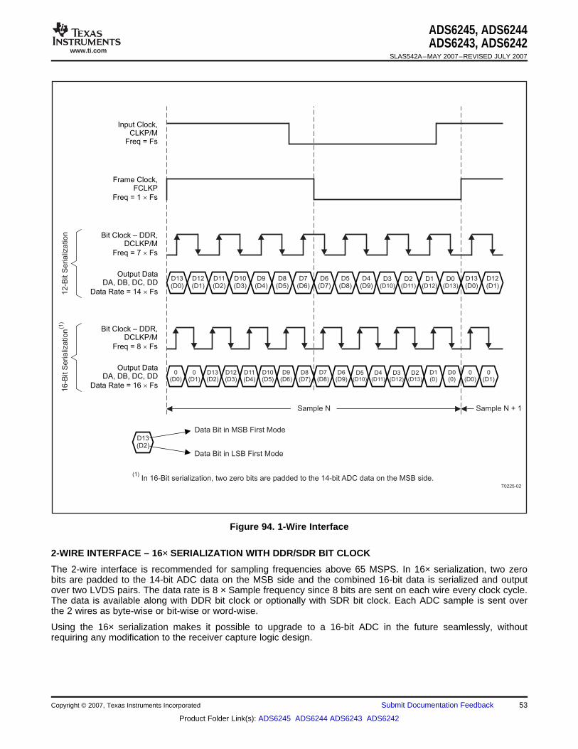
www.ti.com
D13(D0)
0(D0)
D1(0)
0(D0)
0(D1)
D0(0)
0(D1)
D13(D2)
D12(D3)
D11(D4)
D10(D5)
D9(D6)
D7(D8)
D8(D7)
D6(D9)
D5(D10)
D4(D11)
D3(D12)
D2(D13)
D13(D2)
D6(D7)
D10(D3)
D3(D10)
D7(D6)
D0(D13)
D12(D1)
D12(D1)
D5(D8)
D9(D4)
D2(D11)
D11(D2)
D4(D9)
D8(D5)
D1(D12)
D13(D0)
Data Bit in LSB First Mode
Data Bit in MSB First Mode
(1)In 16-Bit serialization, two zero bits are padded to the 14-bit ADC data on the MSB side.
Output DataDA, DB, DC, DD
Data Rate = 16 Fs´
16-B
it S
erializ
ation
(1)
Input Clock,CLKP/M
Freq = Fs
Frame Clock,FCLKP
Freq = 1 Fs´
Bit Clock – DDR,DCLKP/M
Freq = 8 Fs´
T0225-02
Output DataDA, DB, DC, DD
Data Rate = 14 Fs´12-B
it S
erializ
ation Bit Clock – DDR,
DCLKP/M
Freq = 7 Fs´
Sample N Sample N + 1
2-WIRE INTERFACE – 16× SERIALIZATION WITH DDR/SDR BIT CLOCK
ADS6245, ADS6244ADS6243, ADS6242
SLAS542A–MAY 2007–REVISED JULY 2007
Figure 94. 1-Wire Interface
The 2-wire interface is recommended for sampling frequencies above 65 MSPS. In 16× serialization, two zerobits are padded to the 14-bit ADC data on the MSB side and the combined 16-bit data is serialized and outputover two LVDS pairs. The data rate is 8 × Sample frequency since 8 bits are sent on each wire every clock cycle.The data is available along with DDR bit clock or optionally with SDR bit clock. Each ADC sample is sent overthe 2 wires as byte-wise or bit-wise or word-wise.
Using the 16× serialization makes it possible to upgrade to a 16-bit ADC in the future seamlessly, withoutrequiring any modification to the receiver capture logic design.
Copyright © 2007, Texas Instruments Incorporated Submit Documentation Feedback 53
Product Folder Link(s): ADS6245 ADS6244 ADS6243 ADS6242
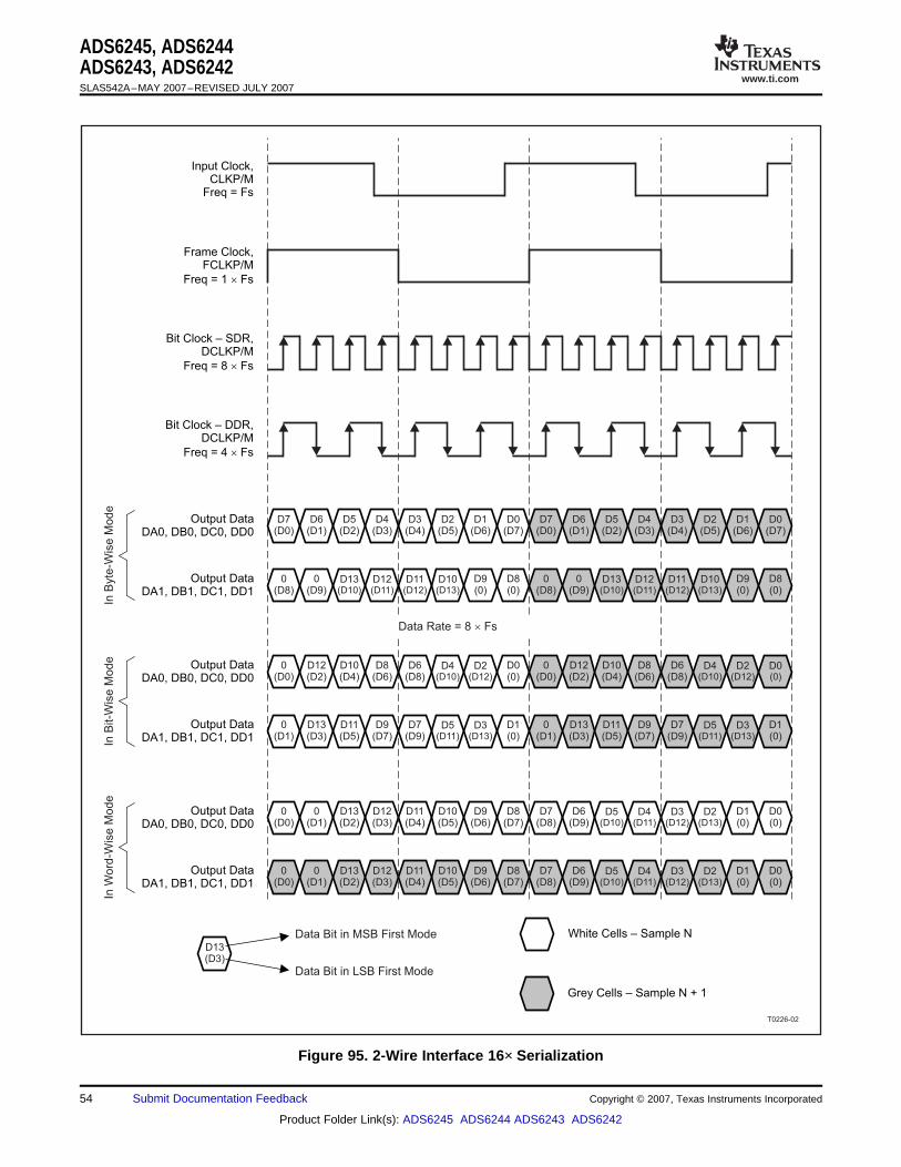
www.ti.com
White Cells – Sample N
Grey Cells – Sample N + 1
0(D0)
0(D0)
D13(D3)
D6(D9)
D6(D9)
D11(D4)
D11(D4)
D2(D13)
D2(D13)
D7(D8)
D7(D8)
0(D1)
0(D1)
D5(D10)
D4(D11)
D5(D10)
D4(D11)
D10(D5)
D10(D5)
D1(0)
D0(0)
D1(0)
D0(0)
D13(D2)
D12(D3)
D13(D2)
D12(D3)
D3(D12)
D3(D12)
D9(D6)
D8(D7)
D9(D6)
D8(D7)
Data Bit in LSB First Mode
Data Bit in MSB First Mode
Output DataDA0, DB0, DC0, DD0
Output DataDA1, DB1, DC1, DD1
In W
ord
-Wis
e M
ode
0(D0)
0(D1)
D12(D2)
D13(D3)
D6(D8)
D7(D9)
D5(D11)
0(D0)
0(D1)
D12(D2)
D13(D3)
D10(D4)
D8(D6)
D11(D5)
D9(D7)
D4(D10)
D4(D10)
D5(D11)
D2(D12)
D0(0)
D10(D4)
D8(D6)
D11(D5)
D9(D7)
D6(D8)
D7(D9)
D2(D12)
D0(0)
D3(D13)
D1(0)
D3(D13)
D1(0)
Output DataDA0, DB0, DC0, DD0
Output DataDA1, DB1, DC1, DD1In
Bit-W
ise M
ode
D7(D0)
D7(D0)
0(D8)
0(D8)
D3(D4)
D3(D4)
D11(D12)
D11(D12)
D6(D1)
D6(D1)
0(D9)
0(D9)
D2(D5)
D2(D5)
D10(D13)
D10(D13)
D5(D2)
D4(D3)
D5(D2)
D4(D3)
D13(D10)
D12(D11)
D13(D10)
D12(D11)
D1(D6)
D0(D7)
D1(D6)
D0(D7)
D9(0)
D8(0)
D9(0)
D8(0)
Output DataDA0, DB0, DC0, DD0
Output DataDA1, DB1, DC1, DD1
In B
yte
-Wis
e M
ode
Data Rate = 8 Fs´
Input Clock,CLKP/M
Freq = Fs
Frame Clock,FCLKP/M
Freq = 1 Fs´
Bit Clock SDR,DCLKP/M
Freq = 8 Fs´
–
Bit Clock DDR,DCLKP/M
Freq = 4 Fs´
–
T0226-02
ADS6245, ADS6244ADS6243, ADS6242SLAS542A–MAY 2007–REVISED JULY 2007
Figure 95. 2-Wire Interface 16× Serialization
54 Submit Documentation Feedback Copyright © 2007, Texas Instruments Incorporated
Product Folder Link(s): ADS6245 ADS6244 ADS6243 ADS6242

www.ti.com
2-WIRE INTERFACE - 14× SERIALIZATION
ADS6245, ADS6244ADS6243, ADS6242
SLAS542A–MAY 2007–REVISED JULY 2007
The 14-bit ADC data is serialized and output over two LVDS pairs. A frame clock at 1× sample frequency is alsoavailable with an SDR bit clock. With DDR bit clock option, the frame clock frequency is 0.5× sample frequency.
The output data rate will be 7 × Sample frequency as 7 data bits are output every clock cycle on each wire. EachADC sample is sent over the 2 wires as byte-wise or bit-wise or word-wise.
Copyright © 2007, Texas Instruments Incorporated Submit Documentation Feedback 55
Product Folder Link(s): ADS6245 ADS6244 ADS6243 ADS6242
www.ti.com
White Cells – Sample N
Grey Cells – Sample N + 1
D13(D0)
D13(D0)
D6(D7)
D6(D7)
D6(D0)
D10(D3)
D10(D3)
D3(D10)
D3(D10)
D7(D6)
D7(D6)
D0(D13)
D0(D13)
D12(D1)
D12(D1)
D12(D1)
D12(D1)
D5(D8)
D5(D8)
D9(D4)
D9(D4)
D2(D11)
D2(D11)
D11(D2)
D11(D2)
D4(D9)
D4(D9)
D8(D5)
D8(D5)
D1(D12)
D1(D12)
D13(D0)
D13(D0)
Data Bit in LSB First Mode
Data Bit in MSB First Mode
Output DataDA0, DB0, DC0, DD0
Output DataDA1, DB1, DC1, DD1
In W
ord
-Wis
e M
od
e
D12(D0)
D13(D1)
D12(D0)
D13(D1)
D6(D6)
D7(D7)
D6(D6)
D7(D7)
D0(D12)
D1(D13)
D0(D12)
D1(D13)
D10(D2)
D11(D3)
D10(D2)
D11(D3)
D10(D2)
D11(D3)
D4(D8)
D5(D9)
D4(D8)
D5(D9)
D8(D4)
D9(D5)
D8(D4)
D9(D5)
D2(D10)
D3(D11)
D2(D10)
D3(D11)
D12(D0)
D13(D1)
Output DataDA0, DB0, DC0, DD0
Output DataDA1, DB1, DC1, DD1In
Bit-W
ise
Mo
de
D6(D0)
D13(D7)
D6(D0)
D13(D7)
D3(D3)
D10(D10)
D3(D3)
D10(D10)
D0(D6)
D7(D13)
D0(D6)
D7(0)
D5(D1)
D12(D8)
D5(D1)
D12(D8)
D5(D1)
D12(D8)
D2(D4)
D9(D11)
D2(D4)
D9(D11)
D4(D2)
D11(D9)
D4(D2)
D11(D9)
D1(D5)
D8(D12)
D1(D5)
D8(0)
D6(D0)
D13(D7)
Output DataDA0, DB0, DC0, DD0
Output DataDA1, DB1, DC1, DD1
In B
yte
-Wis
e M
od
e
Data Rate = 7 Fs´
Input Clock,CLK
Freq = Fs
Frame Clock,FCLK
Freq = 1 Fs´
Bit Clock – SDR,DCLK
Freq = 7 Fs´
T0227-02
ADS6245, ADS6244ADS6243, ADS6242SLAS542A–MAY 2007–REVISED JULY 2007
Figure 96. 2-Wire Interface 14× Serialization - SDR Bit Clock
56 Submit Documentation Feedback Copyright © 2007, Texas Instruments Incorporated
Product Folder Link(s): ADS6245 ADS6244 ADS6243 ADS6242
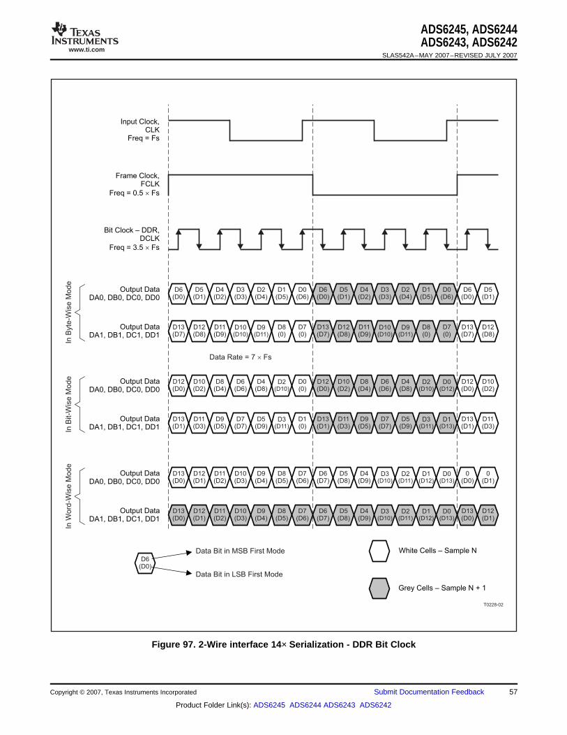
www.ti.com
White Cells – Sample N
Grey Cells – Sample N + 1
D13(D0)
D13(D0)
D6(D7)
D6(D0)
D6(D7)
D10(D3)
D10(D3)
D3(D10)
D3(D10)
D7(D6)
D7(D6)
D0(D13)
D0(D13)
0(D1)
D12(D1)
D12(D1)
D12(D1)
D5(D8)
D5(D8)
D9(D4)
D9(D4)
D2(D11)
D2(D11)
D11(D2)
D11(D2)
D4(D9)
D4(D9)
D8(D5)
D8(D5)
D1(D12)
D1(D12)
0(D0)
D13(D0)
Data Bit in LSB First Mode
Data Bit in MSB First Mode
Output DataDA0, DB0, DC0, DD0
Output DataDA1, DB1, DC1, DD1
In W
ord
-Wis
e M
od
e
D12(D0)
D13(D1)
D12(D0)
D13(D1)
D6(D6)
D7(D7)
D6(D6)
D7(D7)
D0(0)
D1(0)
D0(D12)
D1(D13)
D10(D2)
D11(D3)
D10(D2)
D11(D3)
D10(D2)
D11(D3)
D4(D8)
D5(D9)
D4(D8)
D5(D9)
D8(D4)
D9(D5)
D8(D4)
D9(D5)
D2(D10)
D3(D11)
D2(D10)
D3(D11)
D12(D0)
D13(D1)
Output DataDA0, DB0, DC0, DD0
Output DataDA1, DB1, DC1, DD1In
Bit-W
ise
Mo
de
D6(D0)
D13(D7)
D6(D0)
D13(D7)
D3(D3)
D10(D10)
D3(D3)
D10(D10)
D0(D6)
D7(0)
D0(D6)
D7(0)
D5(D1)
D12(D8)
D5(D1)
D12(D8)
D5(D1)
D12(D8)
D2(D4)
D9(D11)
D2(D4)
D9(D11)
D4(D2)
D11(D9)
D4(D2)
D11(D9)
D1(D5)
D8(0)
D1(D5)
D8(0)
D6(D0)
D13(D7)
Output DataDA0, DB0, DC0, DD0
Output DataDA1, DB1, DC1, DD1
In B
yte
-Wis
e M
od
e
Data Rate = 7 Fs´
Input Clock,CLK
Freq = Fs
Frame Clock,FCLK
Freq = 0.5 Fs´
Bit Clock – DDR,DCLK
Freq = 3.5 Fs´
T0228-02
ADS6245, ADS6244ADS6243, ADS6242
SLAS542A–MAY 2007–REVISED JULY 2007
Figure 97. 2-Wire interface 14× Serialization - DDR Bit Clock
Copyright © 2007, Texas Instruments Incorporated Submit Documentation Feedback 57
Product Folder Link(s): ADS6245 ADS6244 ADS6243 ADS6242
www.ti.com
OUTPUT BIT ORDER
MSB/LSB FIRST
OUTPUT DATA FORMATS
LVDS CURRENT CONTROL
LVDS INTERNAL TERMINATION
ADS6245, ADS6244ADS6243, ADS6242SLAS542A–MAY 2007–REVISED JULY 2007
In the 2-wire interface, three types of bit order are supported - byte-wise, bit-wise and word-wise.
Byte-wise: Each 14-bit sample is split across the 2 wires. Wires DA0 and DB0 carry the 7 LSB bits D6-D0 andwires DA1 and DB1 carry the 7 MSB bits.
Bit-wise: Each 14-bit sample is split across the 2 wires. Wires DA0 and DB0 carry the 7 even bits (D0,D2,D4..)and wires DA1 and DB1 carry the 7 odd bits (D1,D3,D5...).
Word-wise: In this case, all 14-bits of a sample are sent over a single wire. Successive samples are sent overthe 2 wires. For example sample N is sent on wires DA0 and DB0 while sample N+1 is sent over wires DA1 andDB1. The frame clock frequency is 0.5x sampling frequency, with the rising edge aligned with the start of eachword.
By default after reset, the 14-bit ADC data is output serially with the MSB first (D13, D12, D11,...D1,D0). Thedata can be output LSB first also by programming the register bit <MSB_LSB_First>. In the 2-wire mode, the bitorder in each wire is flipped in the LSB first mode.
Two output data formats are supported – 2s complement (default after reset) and offset binary. They can beselected using the serial interface register bit <DF>. In the event of an input voltage overdrive, the digital outputsgo to the appropriate full-scale level. For a positive overdrive, the output code is 0x3FFF in offset binary outputformat, and 0x1FFF in 2s complement output format. For a negative input overdrive, the output code is 0x0000 inoffset binary output format and 0x2000 in 2s complement output format.
The default LVDS buffer current is 3.5 mA. With an external 100-Ω termination resistance, this develops±350-mV logic levels at the receiver. The LVDS buffer currents can also be programmed to 2.5 mA, 3.0 mA and4.5 mA using the register bits <LVDS CURR>. In addition, there exists a current double mode, where the LVDSnominal current is doubled (register bits <CURR DOUBLE>, Table 20).
An internal termination option is available (using the serial interface), by which the LVDS buffers are differentiallyterminated inside the device. Five termination resistances are available – 166, 200, 250, 333, and 500 Ω(nominal with ±20% variation). Any combination of these terminations can be programmed; the effectivetermination will be the parallel combination of the selected resistances. The terminations can be programmedseparately for the clock and data buffers (bits <TERM CLK> and <TERM DATA>, Table 21).
The internal termination helps to absorb any reflections from the receiver end, improving the signal integrity. Thismakes it possible to drive up to 10 pF of load capacitance, compared to only 5 pF without the internaltermination.Figure 98 and Figure 99 show the eye diagram with 5 pF and 10 pF load capacitors (connected fromeach output pin to ground).
With 100-Ω internal and 100-Ω external termination, the voltage swing at the receiver end will be halved(compared to no internal termination). The voltage swing can be restored by using the LVDS current doublemode (bits <CURR DOUBLE>, Table 20).
58 Submit Documentation Feedback Copyright © 2007, Texas Instruments Incorporated
Product Folder Link(s): ADS6245 ADS6244 ADS6243 ADS6242
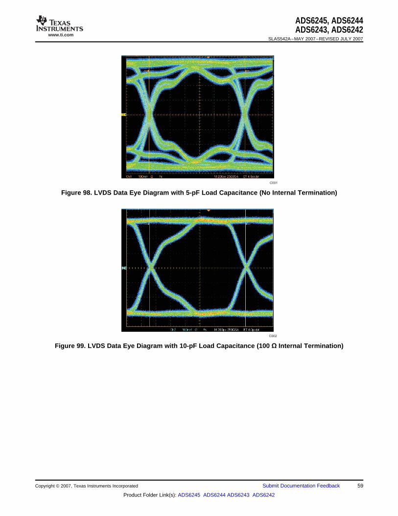
www.ti.com
C001
C002
ADS6245, ADS6244ADS6243, ADS6242
SLAS542A–MAY 2007–REVISED JULY 2007
Figure 98. LVDS Data Eye Diagram with 5-pF Load Capacitance (No Internal Termination)
Figure 99. LVDS Data Eye Diagram with 10-pF Load Capacitance (100 Ω Internal Termination)
Copyright © 2007, Texas Instruments Incorporated Submit Documentation Feedback 59
Product Folder Link(s): ADS6245 ADS6244 ADS6243 ADS6242
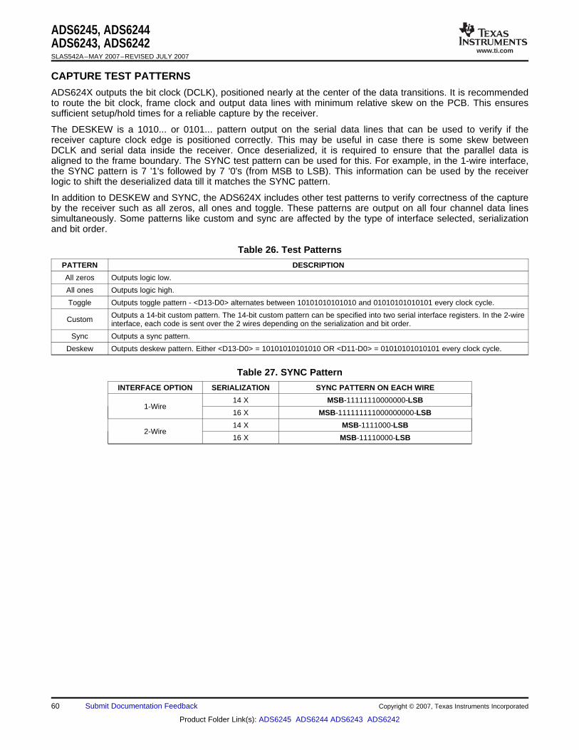
www.ti.com
CAPTURE TEST PATTERNS
ADS6245, ADS6244ADS6243, ADS6242SLAS542A–MAY 2007–REVISED JULY 2007
ADS624X outputs the bit clock (DCLK), positioned nearly at the center of the data transitions. It is recommendedto route the bit clock, frame clock and output data lines with minimum relative skew on the PCB. This ensuressufficient setup/hold times for a reliable capture by the receiver.
The DESKEW is a 1010... or 0101... pattern output on the serial data lines that can be used to verify if thereceiver capture clock edge is positioned correctly. This may be useful in case there is some skew betweenDCLK and serial data inside the receiver. Once deserialized, it is required to ensure that the parallel data isaligned to the frame boundary. The SYNC test pattern can be used for this. For example, in the 1-wire interface,the SYNC pattern is 7 '1's followed by 7 '0's (from MSB to LSB). This information can be used by the receiverlogic to shift the deserialized data till it matches the SYNC pattern.
In addition to DESKEW and SYNC, the ADS624X includes other test patterns to verify correctness of the captureby the receiver such as all zeros, all ones and toggle. These patterns are output on all four channel data linessimultaneously. Some patterns like custom and sync are affected by the type of interface selected, serializationand bit order.
Table 26. Test Patterns
PATTERN DESCRIPTION
All zeros Outputs logic low.
All ones Outputs logic high.
Toggle Outputs toggle pattern - <D13-D0> alternates between 10101010101010 and 01010101010101 every clock cycle.
Outputs a 14-bit custom pattern. The 14-bit custom pattern can be specified into two serial interface registers. In the 2-wireCustom interface, each code is sent over the 2 wires depending on the serialization and bit order.
Sync Outputs a sync pattern.
Deskew Outputs deskew pattern. Either <D13-D0> = 10101010101010 OR <D11-D0> = 01010101010101 every clock cycle.
Table 27. SYNC Pattern
INTERFACE OPTION SERIALIZATION SYNC PATTERN ON EACH WIRE
14 X MSB-11111110000000-LSB1-Wire
16 X MSB-111111111000000000-LSB
14 X MSB-1111000-LSB2-Wire
16 X MSB-11110000-LSB
60 Submit Documentation Feedback Copyright © 2007, Texas Instruments Incorporated
Product Folder Link(s): ADS6245 ADS6244 ADS6243 ADS6242
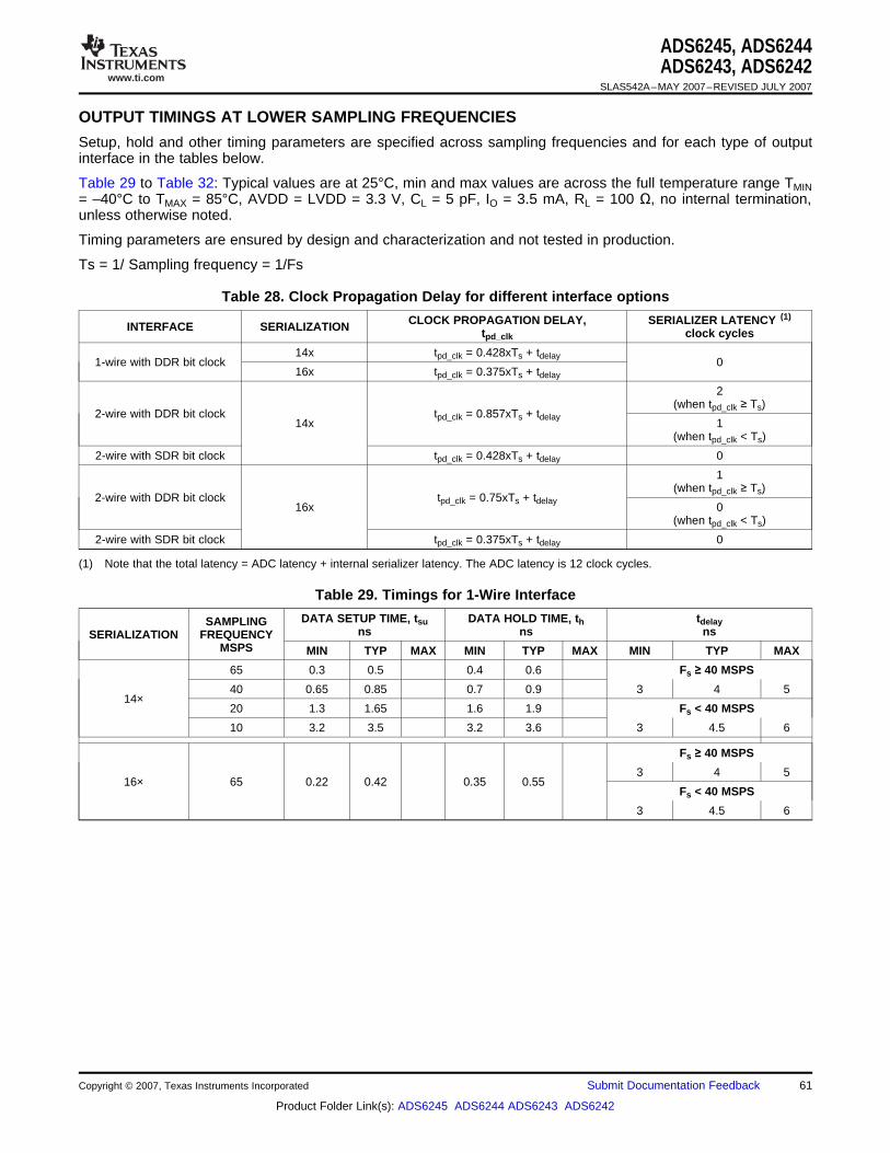
www.ti.com
OUTPUT TIMINGS AT LOWER SAMPLING FREQUENCIES
ADS6245, ADS6244ADS6243, ADS6242
SLAS542A–MAY 2007–REVISED JULY 2007
Setup, hold and other timing parameters are specified across sampling frequencies and for each type of outputinterface in the tables below.
Table 29 to Table 32: Typical values are at 25°C, min and max values are across the full temperature range TMIN= –40°C to TMAX = 85°C, AVDD = LVDD = 3.3 V, CL = 5 pF, IO = 3.5 mA, RL = 100 Ω, no internal termination,unless otherwise noted.
Timing parameters are ensured by design and characterization and not tested in production.
Ts = 1/ Sampling frequency = 1/Fs
Table 28. Clock Propagation Delay for different interface options
CLOCK PROPAGATION DELAY, SERIALIZER LATENCY (1)INTERFACE SERIALIZATION tpd_clk clock cycles
14x tpd_clk = 0.428xTs + tdelay1-wire with DDR bit clock 0
16x tpd_clk = 0.375xTs + tdelay
2(when tpd_clk ≥ Ts)
2-wire with DDR bit clock tpd_clk = 0.857xTs + tdelay14x 1
(when tpd_clk < Ts)
2-wire with SDR bit clock tpd_clk = 0.428xTs + tdelay 0
1(when tpd_clk ≥ Ts)
2-wire with DDR bit clock tpd_clk = 0.75xTs + tdelay16x 0
(when tpd_clk < Ts)
2-wire with SDR bit clock tpd_clk = 0.375xTs + tdelay 0
(1) Note that the total latency = ADC latency + internal serializer latency. The ADC latency is 12 clock cycles.
Table 29. Timings for 1-Wire Interface
DATA SETUP TIME, tsu DATA HOLD TIME, th tdelaySAMPLINGns ns nsSERIALIZATION FREQUENCY
MSPS MIN TYP MAX MIN TYP MAX MIN TYP MAX
65 0.3 0.5 0.4 0.6 Fs ≥ 40 MSPS
40 0.65 0.85 0.7 0.9 3 4 514×
20 1.3 1.65 1.6 1.9 Fs < 40 MSPS
10 3.2 3.5 3.2 3.6 3 4.5 6
Fs ≥ 40 MSPS
3 4 516× 65 0.22 0.42 0.35 0.55
Fs < 40 MSPS
3 4.5 6
Copyright © 2007, Texas Instruments Incorporated Submit Documentation Feedback 61
Product Folder Link(s): ADS6245 ADS6244 ADS6243 ADS6242
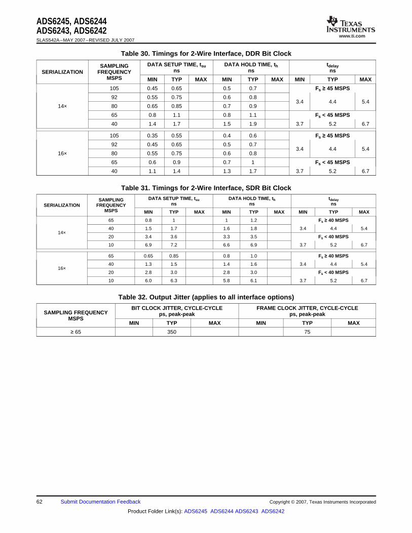
www.ti.com
ADS6245, ADS6244ADS6243, ADS6242SLAS542A–MAY 2007–REVISED JULY 2007
Table 30. Timings for 2-Wire Interface, DDR Bit Clock
DATA SETUP TIME, tsu DATA HOLD TIME, th tdelaySAMPLINGns ns nsSERIALIZATION FREQUENCY
MSPS MIN TYP MAX MIN TYP MAX MIN TYP MAX
105 0.45 0.65 0.5 0.7 Fs ≥ 45 MSPS
92 0.55 0.75 0.6 0.83.4 4.4 5.4
14× 80 0.65 0.85 0.7 0.9
65 0.8 1.1 0.8 1.1 Fs < 45 MSPS
40 1.4 1.7 1.5 1.9 3.7 5.2 6.7
105 0.35 0.55 0.4 0.6 Fs ≥ 45 MSPS
92 0.45 0.65 0.5 0.73.4 4.4 5.4
16× 80 0.55 0.75 0.6 0.8
65 0.6 0.9 0.7 1 Fs < 45 MSPS
40 1.1 1.4 1.3 1.7 3.7 5.2 6.7
Table 31. Timings for 2-Wire Interface, SDR Bit ClockDATA SETUP TIME, tsu DATA HOLD TIME, th tdelaySAMPLING
ns ns nsSERIALIZATION FREQUENCYMSPS MIN TYP MAX MIN TYP MAX MIN TYP MAX
65 0.8 1 1 1.2 Fs ≥ 40 MSPS
40 1.5 1.7 1.6 1.8 3.4 4.4 5.414×
20 3.4 3.6 3.3 3.5 Fs < 40 MSPS
10 6.9 7.2 6.6 6.9 3.7 5.2 6.7
65 0.65 0.85 0.8 1.0 Fs ≥ 40 MSPS
40 1.3 1.5 1.4 1.6 3.4 4.4 5.416×
20 2.8 3.0 2.8 3.0 Fs < 40 MSPS
10 6.0 6.3 5.8 6.1 3.7 5.2 6.7
Table 32. Output Jitter (applies to all interface options)
BIT CLOCK JITTER, CYCLE-CYCLE FRAME CLOCK JITTER, CYCLE-CYCLESAMPLING FREQUENCY ps, peak-peak ps, peak-peak
MSPSMIN TYP MAX MIN TYP MAX
≥ 65 350 75
62 Submit Documentation Feedback Copyright © 2007, Texas Instruments Incorporated
Product Folder Link(s): ADS6245 ADS6244 ADS6243 ADS6242

www.ti.com
BOARD DESIGN CONSIDERATIONS
Grounding
Supply Decoupling
Exposed Thermal Pad
ADS6245, ADS6244ADS6243, ADS6242
SLAS542A–MAY 2007–REVISED JULY 2007
A single ground plane is sufficient to give optimum performance, provided the analog, digital and clock sectionsof the board are cleanly partitioned. Refer to the EVM User Guide (SLAU196) for more layout details.
As the ADS624X already includes internal decoupling, minimal external decoupling can be used without loss inperformance. Note that the decoupling capacitors can help to filter external power supply noise, so the optimumnumber of decoupling capacitors would depend on actual application.
It is recommended to use separate supplies for the analog and digital supply pins to isolate digital switchingnoise from sensitive analog circuitry. In case only a single 3.3V supply is available, it should be routed first toAVDD. It can then be tapped and isolated with a ferrite bead (or inductor) with decoupling capacitor, before beingrouted to LVDD.
For best thermal performance, it is necessary to solder the exposed pad at the bottom of the package to aground plane using multiple vias. For detailed information, see application notes QFN Layout Guidelines(SLOA122A) and QFN/SON PCB Attachment (SLUA271A).
Copyright © 2007, Texas Instruments Incorporated Submit Documentation Feedback 63
Product Folder Link(s): ADS6245 ADS6244 ADS6243 ADS6242
www.ti.com
DEFINITION OF SPECIFICATIONS
SNR 10Log10PSPN (3)
SINAD 10Log10PS
PN PD (4)
ENOB SINAD 1.766.02 (5)
THD 10Log10PSPD (6)
ADS6245, ADS6244ADS6243, ADS6242SLAS542A–MAY 2007–REVISED JULY 2007
Analog Bandwidth – The analog input frequency at which the power of the fundamental is reduced by 3 dB withrespect to the low frequency value.
Aperture Delay – The delay in time between the rising edge of the input sampling clock and the actual time atwhich the sampling occurs.
Aperture Uncertainty (Jitter) – The sample-to-sample variation in aperture delay.
Clock Pulse Width/Duty Cycle – The duty cycle of a clock signal is the ratio of the time the clock signal remainsat a logic high (clock pulse width) to the period of the clock signal. Duty cycle is typically expressed as apercentage. A perfect differential sine-wave clock results in a 50% duty cycle.
Maximum Conversion Rate – The maximum sampling rate at which certified operation is given. All parametrictesting is performed at this sampling rate unless otherwise noted.
Minimum Conversion Rate – The minimum sampling rate at which the ADC functions.
Differential Nonlinearity (DNL) – An ideal ADC exhibits code transitions at analog input values spaced exactly1 LSB apart. The DNL is the deviation of any single step from this ideal value, measured in units of LSBs.
Integral Nonlinearity (INL) – The INL is the deviation of the ADC's transfer function from a best fit linedetermined by a least squares curve fit of that transfer function, measured in units of LSBs.
Gain Error – The gain error is the deviation of the ADC's actual input full-scale range from its ideal value. Thegain error is given as a percentage of the ideal input full-scale range.
Offset Error – The offset error is the difference, given in number of LSBs, between the ADC's actual averageidle channel output code and the ideal average idle channel output code. This quantity is often mapped into mV.
Temperature Drift – The temperature drift coefficient (with respect to gain error and offset error) specifies thechange per degree Celsius of the parameter from TMIN to TMAX. It is calculated by dividing the maximum deviationof the parameter across the TMIN to TMAX range by the difference TMAX–TMIN.
Signal-to-Noise Ratio – SNR is the ratio of the power of the fundamental (PS) to the noise floor power (PN),excluding the power at DC and the first nine harmonics.
SNR is either given in units of dBc (dB to carrier) when the absolute power of the fundamental is used as thereference, or dBFS (dB to full scale) when the power of the fundamental is extrapolated to the converter’sfull-scale range.
Signal-to-Noise and Distortion (SINAD) – SINAD is the ratio of the power of the fundamental (PS) to the powerof all the other spectral components including noise (PN) and distortion (PD), but excluding dc.
SINAD is either given in units of dBc (dB to carrier) when the absolute power of the fundamental is used as thereference, or dBFS (dB to full scale) when the power of the fundamental is extrapolated to the converter'sfull-scale range.
Effective Number of Bits (ENOB) – The ENOB is a measure of a converter’s performance as compared to thetheoretical limit based on quantization noise.
Total Harmonic Distortion (THD) – THD is the ratio of the power of the fundamental (PS) to the power of thefirst nine harmonics (PD).
THD is typically given in units of dBc (dB to carrier).
64 Submit Documentation Feedback Copyright © 2007, Texas Instruments Incorporated
Product Folder Link(s): ADS6245 ADS6244 ADS6243 ADS6242
www.ti.com
PSRR 20Log10 VoutVsup
, expressed in dBc(7)
CMRR 20Log10 VoutVcm_in
, expressed in dBc(8)
ADS6245, ADS6244ADS6243, ADS6242
SLAS542A–MAY 2007–REVISED JULY 2007
Spurious-Free Dynamic Range (SFDR) – The ratio of the power of the fundamental to the highest otherspectral component (either spur or harmonic). SFDR is typically given in units of dBc (dB to carrier).
Two-Tone Intermodulation Distortion – IMD3 is the ratio of the power of the fundamental (at frequencies f1and f2) to the power of the worst spectral component at either frequency 2f1–f2 or 2f2–f1. IMD3 is either given inunits of dBc (dB to carrier) when the absolute power of the fundamental is used as the reference, or dBFS (dB tofull scale) when the power of the fundamental is extrapolated to the converter’s full-scale range.
DC Power Supply Rejection Ratio (DC PSRR) – The DC PSSR is the ratio of the change in offset error to achange in analog supply voltage. The DC PSRR is typically given in units of mV/V.
AC Power Supply Rejection Ratio (AC PSRR) – AC PSRR is the measure of rejection of variations in thesupply voltage by the ADC. If ΔVsup is the change in supply voltage and ΔVout is the resultant change of theADC output code (referred to the input), then
Voltage Overload Recovery – The number of clock cycles taken to recover to less than 1% error after anoverload on the analog inputs. This is tested by separately applying a sine wave signal with 6dB positive andnegative overload. The deviation of the first few samples after the overload (from their expected values) is noted.
Common Mode Rejection Ratio (CMRR) – CMRR is the measure of rejection of variations in the analog inputcommon-mode by the ADC. If ΔVcm_in is the change in the common-mode voltage of the input pins and ΔVoutis the resultant change of the ADC output code (referred to the input), then
Cross-Talk (only for multi-channel ADC)– This is a measure of the internal coupling of a signal from adjacentchannel into the channel of interest. It is specified separately for coupling from the immediate neighbouringchannel (near-channel) and for coupling from channel across the package (far-channel). It is usually measuredby applying a full-scale signal in the adjacent channel. Cross-talk is the ratio of the power of the coupling signal(as measured at the output of the channel of interest) to the power of the signal applied at the adjacent channelinput. It is typically expressed in dBc.
Copyright © 2007, Texas Instruments Incorporated Submit Documentation Feedback 65
Product Folder Link(s): ADS6245 ADS6244 ADS6243 ADS6242


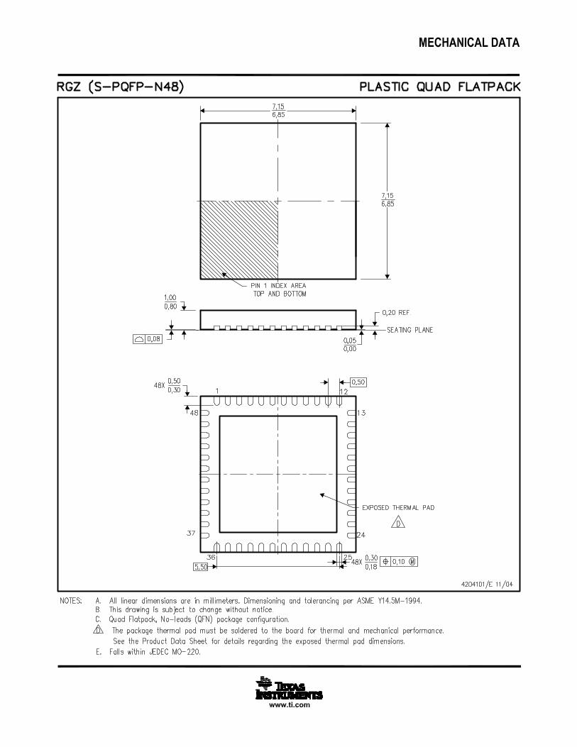
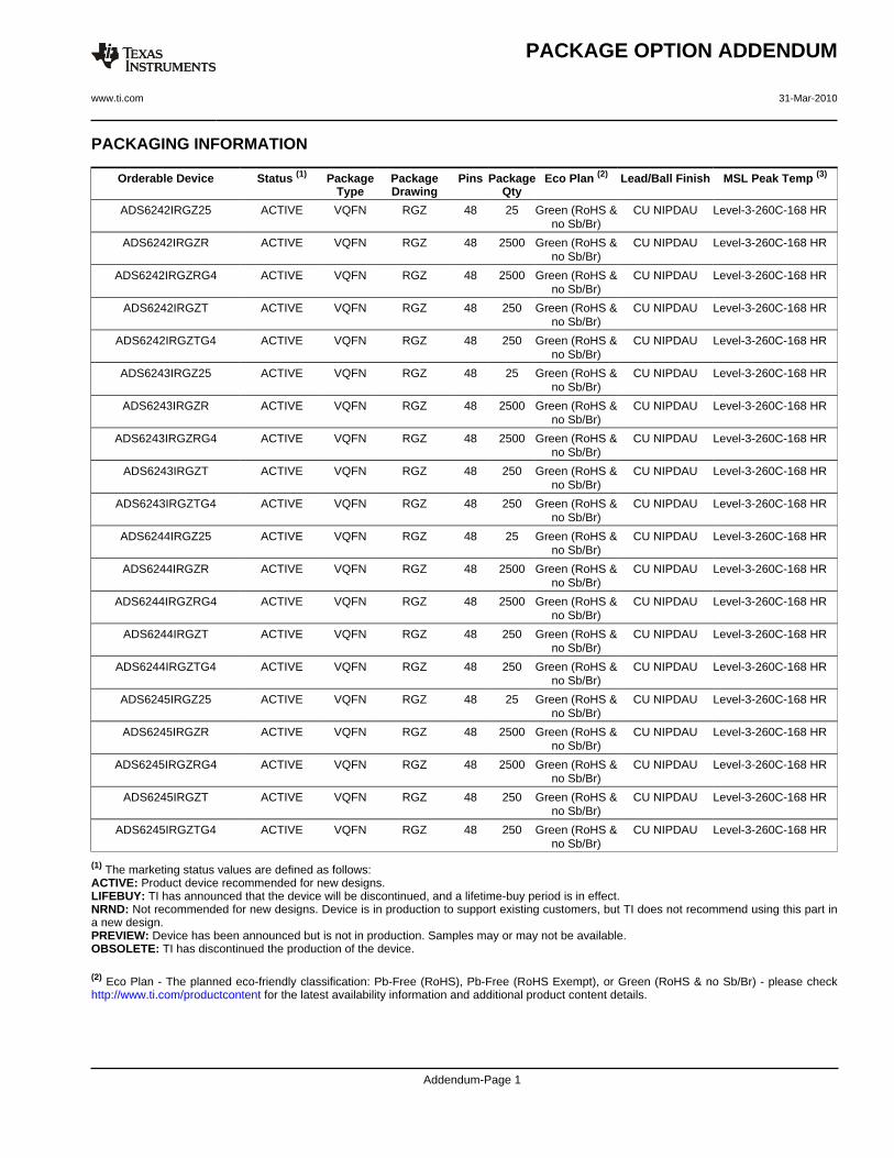
PACKAGING INFORMATION
Orderable Device Status (1) PackageType
PackageDrawing
Pins PackageQty
Eco Plan (2) Lead/Ball Finish MSL Peak Temp (3)
ADS6242IRGZ25 ACTIVE VQFN RGZ 48 25 Green (RoHS &no Sb/Br)
CU NIPDAU Level-3-260C-168 HR
ADS6242IRGZR ACTIVE VQFN RGZ 48 2500 Green (RoHS &no Sb/Br)
CU NIPDAU Level-3-260C-168 HR
ADS6242IRGZRG4 ACTIVE VQFN RGZ 48 2500 Green (RoHS &no Sb/Br)
CU NIPDAU Level-3-260C-168 HR
ADS6242IRGZT ACTIVE VQFN RGZ 48 250 Green (RoHS &no Sb/Br)
CU NIPDAU Level-3-260C-168 HR
ADS6242IRGZTG4 ACTIVE VQFN RGZ 48 250 Green (RoHS &no Sb/Br)
CU NIPDAU Level-3-260C-168 HR
ADS6243IRGZ25 ACTIVE VQFN RGZ 48 25 Green (RoHS &no Sb/Br)
CU NIPDAU Level-3-260C-168 HR
ADS6243IRGZR ACTIVE VQFN RGZ 48 2500 Green (RoHS &no Sb/Br)
CU NIPDAU Level-3-260C-168 HR
ADS6243IRGZRG4 ACTIVE VQFN RGZ 48 2500 Green (RoHS &no Sb/Br)
CU NIPDAU Level-3-260C-168 HR
ADS6243IRGZT ACTIVE VQFN RGZ 48 250 Green (RoHS &no Sb/Br)
CU NIPDAU Level-3-260C-168 HR
ADS6243IRGZTG4 ACTIVE VQFN RGZ 48 250 Green (RoHS &no Sb/Br)
CU NIPDAU Level-3-260C-168 HR
ADS6244IRGZ25 ACTIVE VQFN RGZ 48 25 Green (RoHS &no Sb/Br)
CU NIPDAU Level-3-260C-168 HR
ADS6244IRGZR ACTIVE VQFN RGZ 48 2500 Green (RoHS &no Sb/Br)
CU NIPDAU Level-3-260C-168 HR
ADS6244IRGZRG4 ACTIVE VQFN RGZ 48 2500 Green (RoHS &no Sb/Br)
CU NIPDAU Level-3-260C-168 HR
ADS6244IRGZT ACTIVE VQFN RGZ 48 250 Green (RoHS &no Sb/Br)
CU NIPDAU Level-3-260C-168 HR
ADS6244IRGZTG4 ACTIVE VQFN RGZ 48 250 Green (RoHS &no Sb/Br)
CU NIPDAU Level-3-260C-168 HR
ADS6245IRGZ25 ACTIVE VQFN RGZ 48 25 Green (RoHS &no Sb/Br)
CU NIPDAU Level-3-260C-168 HR
ADS6245IRGZR ACTIVE VQFN RGZ 48 2500 Green (RoHS &no Sb/Br)
CU NIPDAU Level-3-260C-168 HR
ADS6245IRGZRG4 ACTIVE VQFN RGZ 48 2500 Green (RoHS &no Sb/Br)
CU NIPDAU Level-3-260C-168 HR
ADS6245IRGZT ACTIVE VQFN RGZ 48 250 Green (RoHS &no Sb/Br)
CU NIPDAU Level-3-260C-168 HR
ADS6245IRGZTG4 ACTIVE VQFN RGZ 48 250 Green (RoHS &no Sb/Br)
CU NIPDAU Level-3-260C-168 HR
(1) The marketing status values are defined as follows:ACTIVE: Product device recommended for new designs.LIFEBUY: TI has announced that the device will be discontinued, and a lifetime-buy period is in effect.NRND: Not recommended for new designs. Device is in production to support existing customers, but TI does not recommend using this part ina new design.PREVIEW: Device has been announced but is not in production. Samples may or may not be available.OBSOLETE: TI has discontinued the production of the device.
(2) Eco Plan - The planned eco-friendly classification: Pb-Free (RoHS), Pb-Free (RoHS Exempt), or Green (RoHS & no Sb/Br) - please checkhttp://www.ti.com/productcontent for the latest availability information and additional product content details.
PACKAGE OPTION ADDENDUM
www.ti.com 31-Mar-2010
Addendum-Page 1
TBD: The Pb-Free/Green conversion plan has not been defined.Pb-Free (RoHS): TI's terms "Lead-Free" or "Pb-Free" mean semiconductor products that are compatible with the current RoHS requirementsfor all 6 substances, including the requirement that lead not exceed 0.1% by weight in homogeneous materials. Where designed to be solderedat high temperatures, TI Pb-Free products are suitable for use in specified lead-free processes.Pb-Free (RoHS Exempt): This component has a RoHS exemption for either 1) lead-based flip-chip solder bumps used between the die andpackage, or 2) lead-based die adhesive used between the die and leadframe. The component is otherwise considered Pb-Free (RoHScompatible) as defined above.Green (RoHS & no Sb/Br): TI defines "Green" to mean Pb-Free (RoHS compatible), and free of Bromine (Br) and Antimony (Sb) based flameretardants (Br or Sb do not exceed 0.1% by weight in homogeneous material)
(3) MSL, Peak Temp. -- The Moisture Sensitivity Level rating according to the JEDEC industry standard classifications, and peak soldertemperature.
Important Information and Disclaimer:The information provided on this page represents TI's knowledge and belief as of the date that it isprovided. TI bases its knowledge and belief on information provided by third parties, and makes no representation or warranty as to theaccuracy of such information. Efforts are underway to better integrate information from third parties. TI has taken and continues to takereasonable steps to provide representative and accurate information but may not have conducted destructive testing or chemical analysis onincoming materials and chemicals. TI and TI suppliers consider certain information to be proprietary, and thus CAS numbers and other limitedinformation may not be available for release.
In no event shall TI's liability arising out of such information exceed the total purchase price of the TI part(s) at issue in this document sold by TIto Customer on an annual basis.
PACKAGE OPTION ADDENDUM
www.ti.com 31-Mar-2010
Addendum-Page 2
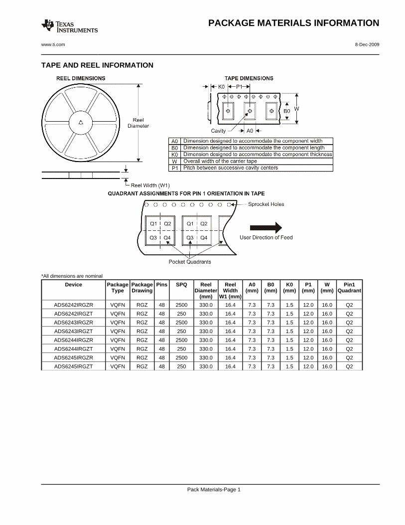
TAPE AND REEL INFORMATION
*All dimensions are nominal
Device PackageType
PackageDrawing
Pins SPQ ReelDiameter
(mm)
ReelWidth
W1 (mm)
A0(mm)
B0(mm)
K0(mm)
P1(mm)
W(mm)
Pin1Quadrant
ADS6242IRGZR VQFN RGZ 48 2500 330.0 16.4 7.3 7.3 1.5 12.0 16.0 Q2
ADS6242IRGZT VQFN RGZ 48 250 330.0 16.4 7.3 7.3 1.5 12.0 16.0 Q2
ADS6243IRGZR VQFN RGZ 48 2500 330.0 16.4 7.3 7.3 1.5 12.0 16.0 Q2
ADS6243IRGZT VQFN RGZ 48 250 330.0 16.4 7.3 7.3 1.5 12.0 16.0 Q2
ADS6244IRGZR VQFN RGZ 48 2500 330.0 16.4 7.3 7.3 1.5 12.0 16.0 Q2
ADS6244IRGZT VQFN RGZ 48 250 330.0 16.4 7.3 7.3 1.5 12.0 16.0 Q2
ADS6245IRGZR VQFN RGZ 48 2500 330.0 16.4 7.3 7.3 1.5 12.0 16.0 Q2
ADS6245IRGZT VQFN RGZ 48 250 330.0 16.4 7.3 7.3 1.5 12.0 16.0 Q2
PACKAGE MATERIALS INFORMATION
www.ti.com 8-Dec-2009
Pack Materials-Page 1
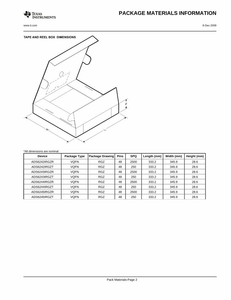
*All dimensions are nominal
Device Package Type Package Drawing Pins SPQ Length (mm) Width (mm) Height (mm)
ADS6242IRGZR VQFN RGZ 48 2500 333.2 345.9 28.6
ADS6242IRGZT VQFN RGZ 48 250 333.2 345.9 28.6
ADS6243IRGZR VQFN RGZ 48 2500 333.2 345.9 28.6
ADS6243IRGZT VQFN RGZ 48 250 333.2 345.9 28.6
ADS6244IRGZR VQFN RGZ 48 2500 333.2 345.9 28.6
ADS6244IRGZT VQFN RGZ 48 250 333.2 345.9 28.6
ADS6245IRGZR VQFN RGZ 48 2500 333.2 345.9 28.6
ADS6245IRGZT VQFN RGZ 48 250 333.2 345.9 28.6
PACKAGE MATERIALS INFORMATION
www.ti.com 8-Dec-2009
Pack Materials-Page 2
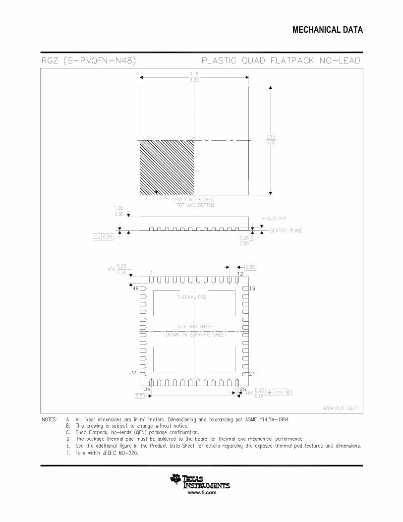
IMPORTANT NOTICE
Texas Instruments Incorporated and its subsidiaries (TI) reserve the right to make corrections, modifications, enhancements, improvements,and other changes to its products and services at any time and to discontinue any product or service without notice. Customers shouldobtain the latest relevant information before placing orders and should verify that such information is current and complete. All products aresold subject to TI’s terms and conditions of sale supplied at the time of order acknowledgment.
TI warrants performance of its hardware products to the specifications applicable at the time of sale in accordance with TI’s standardwarranty. Testing and other quality control techniques are used to the extent TI deems necessary to support this warranty. Except wheremandated by government requirements, testing of all parameters of each product is not necessarily performed.
TI assumes no liability for applications assistance or customer product design. Customers are responsible for their products andapplications using TI components. To minimize the risks associated with customer products and applications, customers should provideadequate design and operating safeguards.
TI does not warrant or represent that any license, either express or implied, is granted under any TI patent right, copyright, mask work right,or other TI intellectual property right relating to any combination, machine, or process in which TI products or services are used. Informationpublished by TI regarding third-party products or services does not constitute a license from TI to use such products or services or awarranty or endorsement thereof. Use of such information may require a license from a third party under the patents or other intellectualproperty of the third party, or a license from TI under the patents or other intellectual property of TI.
Reproduction of TI information in TI data books or data sheets is permissible only if reproduction is without alteration and is accompaniedby all associated warranties, conditions, limitations, and notices. Reproduction of this information with alteration is an unfair and deceptivebusiness practice. TI is not responsible or liable for such altered documentation. Information of third parties may be subject to additionalrestrictions.
Resale of TI products or services with statements different from or beyond the parameters stated by TI for that product or service voids allexpress and any implied warranties for the associated TI product or service and is an unfair and deceptive business practice. TI is notresponsible or liable for any such statements.
TI products are not authorized for use in safety-critical applications (such as life support) where a failure of the TI product would reasonablybe expected to cause severe personal injury or death, unless officers of the parties have executed an agreement specifically governingsuch use. Buyers represent that they have all necessary expertise in the safety and regulatory ramifications of their applications, andacknowledge and agree that they are solely responsible for all legal, regulatory and safety-related requirements concerning their productsand any use of TI products in such safety-critical applications, notwithstanding any applications-related information or support that may beprovided by TI. Further, Buyers must fully indemnify TI and its representatives against any damages arising out of the use of TI products insuch safety-critical applications.
TI products are neither designed nor intended for use in military/aerospace applications or environments unless the TI products arespecifically designated by TI as military-grade or "enhanced plastic." Only products designated by TI as military-grade meet militaryspecifications. Buyers acknowledge and agree that any such use of TI products which TI has not designated as military-grade is solely atthe Buyer's risk, and that they are solely responsible for compliance with all legal and regulatory requirements in connection with such use.
TI products are neither designed nor intended for use in automotive applications or environments unless the specific TI products aredesignated by TI as compliant with ISO/TS 16949 requirements. Buyers acknowledge and agree that, if they use any non-designatedproducts in automotive applications, TI will not be responsible for any failure to meet such requirements.
Following are URLs where you can obtain information on other Texas Instruments products and application solutions:
Products Applications
Audio www.ti.com/audio Communications and Telecom www.ti.com/communications
Amplifiers amplifier.ti.com Computers and Peripherals www.ti.com/computers
Data Converters dataconverter.ti.com Consumer Electronics www.ti.com/consumer-apps
DLP® Products www.dlp.com Energy and Lighting www.ti.com/energy
DSP dsp.ti.com Industrial www.ti.com/industrial
Clocks and Timers www.ti.com/clocks Medical www.ti.com/medical
Interface interface.ti.com Security www.ti.com/security
Logic logic.ti.com Space, Avionics and Defense www.ti.com/space-avionics-defense
Power Mgmt power.ti.com Transportation and www.ti.com/automotiveAutomotive
Microcontrollers microcontroller.ti.com Video and Imaging www.ti.com/video
RFID www.ti-rfid.com Wireless www.ti.com/wireless-apps
RF/IF and ZigBee® Solutions www.ti.com/lprf
TI E2E Community Home Page e2e.ti.com
Mailing Address: Texas Instruments, Post Office Box 655303, Dallas, Texas 75265Copyright © 2011, Texas Instruments Incorporated