dsPIC33EPXXXGP50X, dsPIC33EPXXXMC20X/50X and PIC24EPXXXGP...
36
2011-2017 Microchip Technology Inc. DS80000533M-page 1 dsPIC33EPXXXGP50X, dsPIC33EPXXXMC20X/50X and PIC24EPXXXGP/MC20X The dsPIC33EPXXXGP50X, dsPIC33EPXXXMC20X/50X and PIC24EPXXXGP/MC20X family devices that you have received conform functionally to the current Device Data Sheet (DS70000657H), except for the anomalies described in this document. The silicon issues discussed in the following pages are for silicon revisions with the Device and Revision IDs listed in Table 1. The silicon issues are summarized in Table 2. The errata described in this document will be addressed in future revisions of dsPIC33EPXXXGP50X, dsPIC33EPXXXMC20X/50X and PIC24EPXXXGP/MC20X silicon. Data Sheet clarifications and corrections start on Page 27, following the discussion of silicon issues. The silicon revision level can be identified using the current version of MPLAB ® IDE and Microchip’s programmers, debuggers and emulation tools, which are available at the Microchip corporate web site (www.microchip.com). For example, to identify the silicon revision level using MPLAB IDE in conjunction with MPLAB ICD 3 or PICkit™ 3: 1. Using the appropriate interface, connect the device to the MPLAB ICD 3 programmer/debugger or PICkit 3. 2. From the main menu in MPLAB IDE, select Configure>Select Device , and then select the target part number in the dialog box. 3. Select the MPLAB hardware tool (Debugger>Select Tool ). 4. Perform a “Connect” operation to the device (Debugger>Connect ). Depending on the devel- opment tool used, the part number and Device Revision ID value appear in the Output window. The Device and Revision ID values for the various silicon revisions are shown in Table 1. Note: This document summarizes all silicon errata issues from all revisions of silicon, previous as well as current. The current silicon revision levels are: dsPIC33/PIC24EP32: A3, A8 dsPIC33/PIC24EP64: A2, A3, A8 dsPIC33/PIC24EP128: A3, A8 dsPIC33/PIC24EP256: A3, A8, A9 dsPIC33/PIC24EP512: A7 “N/A” indicates that the device family is not released, or that the particular silicon issue does not apply to this family. Note: If you are unable to extract the silicon revision level, please contact your local Microchip sales office for assistance. dsPIC33EPXXXGP50X, dsPIC33EPXXXMC20X/50X and PIC24EPXXXGP/MC20X Family Silicon Errata and Data Sheet Clarification
Transcript of dsPIC33EPXXXGP50X, dsPIC33EPXXXMC20X/50X and PIC24EPXXXGP...

dsPIC33EPXXXGP50X, dsPIC33EPXXXMC20X/50X
and PIC24EPXXXGP/MC20X
dsPIC33EPXXXGP50X, dsPIC33EPXXXMC20X/50X and PIC24EPXXXGP/MC20X Family Silicon Errata and Data Sheet Clarification
The dsPIC33EPXXXGP50X, dsPIC33EPXXXMC20X/50X and PIC24EPXXXGP/MC20X family devices that you have received conform functionally to the current Device Data Sheet (DS70000657H), except for the anomalies described in this document.
The silicon issues discussed in the following pages are for silicon revisions with the Device and Revision IDs listed in Table 1. The silicon issues are summarized in Table 2.
The errata described in this document will be addressed in future revisions ofdsPIC33EPXXXGP50X, dsPIC33EPXXXMC20X/50X and PIC24EPXXXGP/MC20X silicon.
Data Sheet clarifications and corrections start on Page 27, following the discussion of silicon issues.
The silicon revision level can be identified using the current version of MPLAB® IDE and Microchip’s programmers, debuggers and emulation tools, which are available at the Microchip corporate web site (www.microchip.com).
For example, to identify the silicon revision level using MPLAB IDE in conjunction with MPLAB ICD 3 or PICkit™ 3:
1. Using the appropriate interface, connect the device to the MPLAB ICD 3 programmer/debugger or PICkit 3.
2. From the main menu in MPLAB IDE, select Configure>Select Device, and then select the target part number in the dialog box.
3. Select the MPLAB hardware tool (Debugger>Select Tool).
4. Perform a “Connect” operation to the device (Debugger>Connect). Depending on the devel-opment tool used, the part number and Device Revision ID value appear in the Output window.
The Device and Revision ID values for the various silicon revisions are shown in Table 1.
Note: This document summarizes all silicon errata issues from all revisions of silicon, previous as well as current. The current silicon revision levels are:dsPIC33/PIC24EP32: A3, A8dsPIC33/PIC24EP64: A2, A3, A8dsPIC33/PIC24EP128: A3, A8dsPIC33/PIC24EP256: A3, A8, A9dsPIC33/PIC24EP512: A7“N/A” indicates that the device family is not released, or that the particular silicon issue does not apply to this family.
Note: If you are unable to extract the silicon revision level, please contact your local Microchip sales office for assistance.
2011-2017 Microchip Technology Inc. DS80000533M-page 1

dsPIC33EPXXXGP50X, dsPIC33EPXXXMC20X/50X and PIC24EPXXXGP/MC20X
TABLE 1: SILICON DEVREV VALUES
Part Number Device ID(1) Silicon Revision/Device ID(2)
PIC24EP32GP202 0x1C19
—A3
0x4003A8
0x4008—
PIC24EP32GP203 0x1C1A
PIC24EP32GP204 0x1C18
dsPIC33EP32GP502 0x1C0D
dsPIC33EP32GP503 0x1C0E
dsPIC33EP32GP504 0x1C0C
PIC24EP32MC202 0x1C11
PIC24EP32MC203 0x1C12
PIC24EP32MC204 0x1C10
dsPIC33EP32MC202 0x1C01
dsPIC33EP32MC203 0x1C02
dsPIC33EP32MC204 0x1C00
dsPIC33EP32MC502 0x1C05
dsPIC33EP32MC503 0x1C06
dsPIC33EP32MC504 0x1C04
dsPIC33EP32MC506 0x1D27
PIC24EP64GP202 0x1D39
A20x4002
A30x4003
A80x4008
—
PIC24EP64GP203 0x1D3A
PIC24EP64GP204 0x1D38
PIC24EP64GP206 0x1D3B
dsPIC33EP64GP502 0x1D2D
dsPIC33EP64GP503 0x1D2E
dsPIC33EP64GP504 0x1D2C
dsPIC33EP64GP506 0x1D2F
PIC24EP64MC202 0x1D31
PIC24EP64MC203 0x1D32
PIC24EP64MC204 0x1D30
PIC24EP64MC206 0x1D33
dsPIC33EP64MC202 0x1D21
dsPIC33EP64MC203 0x1D22
dsPIC33EP64MC204 0x1D20
dsPIC33EP64MC206 0x1D23
dsPIC33EP64MC502 0x1D25
dsPIC33EP64MC503 0x1D26
dsPIC33EP64MC504 0x1D24
dsPIC33EP64MC506 0x1D27
Note 1: The Device and Revision IDs (DEVID and DEVREV) are located at the last two implemented addresses in program memory.
2: Refer to the “dsPIC33E/PIC24E Flash Programming Specification for Devices with Volatile Configuration Bits” (DS70663) for detailed information on Device and Revision IDs for your specific device.
DS80000533M-page 2 2011-2017 Microchip Technology Inc.

dsPIC33EPXXXGP50X, dsPIC33EPXXXMC20X/50X and PIC24EPXXXGP/MC20X
PIC24EP128GP202 0x1E59
—A3
0x4003A8
0x4008—
PIC24EP128GP204 0x1E58
PIC24EP128GP206 0x1E5B
dsPIC33EP128GP502 0x1E4D
dsPIC33EP128GP504 0x1E4C
dsPIC33EP128GP506 0x1E4F
PIC24EP128MC202 0x1E51
PIC24EP128MC204 0x1E50
PIC24EP128MC206 0x1E53
dsPIC33EP128MC202 0x1E41
dsPIC33EP128MC204 0x1E40
dsPIC33EP128MC206 0x1E43
dsPIC33EP128MC502 0x1E45
dsPIC33EP128MC504 0x1E44
dsPIC33EP128MC506 0x1E47
PIC24EP256GP202 0x1F79
—A3
0x4003A8
0x4008A9
0x4009
PIC24EP256GP204 0x1F78
PIC24EP256GP206 0x1F7B
dsPIC33EP256GP502 0x1F6D
dsPIC33EP256GP504 0x1F6C
dsPIC33EP256GP506 0x1F6F
PIC24EP256MC202 0x1F71
PIC24EP256MC204 0x1F70
PIC24EP256MC206 0x1F73
dsPIC33EP256MC202 0x1F61
dsPIC33EP256MC204 0x1F60
dsPIC33EP256MC206 0x1F63
dsPIC33EP256MC502 0x1F65
dsPIC33EP256MC504 0x1F64
dsPIC33EP256MC506 0x1F67
TABLE 1: SILICON DEVREV VALUES (CONTINUED)
Part Number Device ID(1) Silicon Revision/Device ID(2)
Note 1: The Device and Revision IDs (DEVID and DEVREV) are located at the last two implemented addresses in program memory.
2: Refer to the “dsPIC33E/PIC24E Flash Programming Specification for Devices with Volatile Configuration Bits” (DS70663) for detailed information on Device and Revision IDs for your specific device.
2011-2017 Microchip Technology Inc. DS80000533M-page 3

dsPIC33EPXXXGP50X, dsPIC33EPXXXMC20X/50X and PIC24EPXXXGP/MC20X
PIC24EP512GP202 0x1799
—A7
0x4007— —
PIC24EP512GP204 0x1798
PIC24EP512GP206 0x179B
dsPIC33EP512GP502 0x178D
dsPIC33EP512GP504 0x178C
dsPIC33EP512GP506 0x178F
PIC24EP512MC202 0x1791
PIC24EP512MC204 0x1790
PIC24EP512MC206 0x1793
dsPIC33EP512MC202 0x1781
dsPIC33EP512MC204 0x1780
dsPIC33EP512MC206 0x1783
dsPIC33EP512MC502 0x1785
dsPIC33EP512MC504 0x1784
dsPIC33EP512MC506 0x1787
TABLE 1: SILICON DEVREV VALUES (CONTINUED)
Part Number Device ID(1) Silicon Revision/Device ID(2)
Note 1: The Device and Revision IDs (DEVID and DEVREV) are located at the last two implemented addresses in program memory.
2: Refer to the “dsPIC33E/PIC24E Flash Programming Specification for Devices with Volatile Configuration Bits” (DS70663) for detailed information on Device and Revision IDs for your specific device.
DS80000533M-page 4 2011-2017 Microchip Technology Inc.

dsPIC33EPXXXGP50X, dsPIC33EPXXXMC20X/50X and PIC24EPXXXGP/MC20X
TABLE 2: SILICON ISSUE SUMMARY
Module FeatureItem
NumberIssue Summary
CPU div.sd 1. When using the div.sd instruction, the Overflow bit is not getting set when an overflow occurs.
CPU DO Loop 2. PSV access, including Table Reads or Writes in the first or last instruction of a DO loop, is not allowed.
SPI Frame Sync Pulse 3. Frame Sync pulse is not generated in Master mode when FRMPOL = 0.
SPI Frame Sync Pulse 4. When in SPI Slave mode, with the Frame Sync pulse set as an input, FRMDLY must be set to ‘0’.
UART TX Interrupt 5. A Transmit (TX) interrupt may occur before the data transmission is complete.
Power System Flash Regulator 6. The VREGSF (RCON<11>) bit always reads back as ‘0’.
ADC DONE bit 7. The ADC Conversion Status bit (DONE) does not work when an external interrupt is selected as the ADC trigger source.
PTG Strobe Output 8. Strobe output pulse width is incorrectly dependent on the PTGPWD<3:0> (PTGCON<7:4>) bits setting.
Op Amp Enabling Op Amp mode
9. When using any of these op amp modules, or Analog Channels AN0, AN3 or AN6, to sample external signals, bit 11 of the CMxCON register must be set to ‘1’.
Op Amp AC/DC Electrical Characteristics
10. The AC/DC electrical characteristics for the op amp module (and the related ADC specifications) are not within the specifications published in the current data sheet.
PWM Dead-Time Compensation
11. Dead-time compensation is not enabled for Center-Aligned PWM mode.
Flash Flash Programming 12. The Stall mechanism may not function properly when erasing or programming Flash memory.
QEI Index Counter 13. The QEI Index Counter does not count correctly in Quadrature Detector mode.
QEI Modulo Mode 14. Modulo mode functionality is incorrect when the count polarity bit is set.
PWM Master Time Base Mode
15. In Master Time Base mode, writing to the period register and any other timing parameter of the PWMx module, will cause the update of the other timing parameter to take effect one PWM cycle after the period update is effective.
ADC 1.1 Msps Sampling 16. Selecting the same ANx input (AN0 or AN3) for CH0 and CH1 to achieve a 1.1 Msps sampling rate results in erroneous readings for CH1.
ADC Channel Scan 17. Channel scanning is limited to AN0 through AN15.
Output Compare Interrupt 18. Under certain circumstances, an output compare match may cause the Output Compare x Interrupt Flag (OCxIF) bit to become set prior to the Change-of-State (COS) of the OCx pin.
CAN DMA 19. Write collisions on a DMA-enabled CAN module does not generate DMAC error traps.
PWM Immediate Update 20. Dead time is not asserted when PDCx is updated to cause an immediate transition on the PWMxH and PWMxL outputs.
PWM Center-Aligned Mode
21. PWMxH is asserted for 100% of the PWM period in Complementary mode under certain circumstances.
PWM Complementary Mode
22. With dead time greater than zero, 0% and 100% duty cycle cannot be obtained on PWMxL and PWMxH outputs.
2011-2017 Microchip Technology Inc. DS80000533M-page 5

dsPIC33EPXXXGP50X, dsPIC33EPXXXMC20X/50X and PIC24EPXXXGP/MC20X
CPU Program Memory 23. Address error trap may occur while accessing certain program memory locations.
PWM Center-Aligned Mode
24. Updates to active MDC/PDCx/ALTDTRx/PHASEx registers occur only once every two PWM periods.
PWM Independent Time Base Mode
25. Under certain circumstances, updates to the OVRENH and OVRENL bits may be ignored by the PWMx module.
PWM Center-Aligned Mode
26. PHASEx register updates are delayed.
CTMU ADC Operation 27. CTMU does not work with the ADC Converter in 12-bit mode.
Input Capture External Synchronization
28. Input capture and output compare modules cannot be synchronized.
JTAG I/O 29. MCLR pin operation may be disabled.
I/O Pin Functions that are Not 5V Tolerant
30. Select pins are not 5V tolerant.
JTAG I/O 31. Active-high logic pulse on the I/O pin with TMS function at POR.
QEI Velocity Counter 32. Under certain circumstances, the Velocity Counter 1 register (VEL1CNT) misses count pulses.
QEI Position Capture 33. Under certain conditions, the captured position may be off by ±1 count.
QEI Position Capture 34. Position count captured at the rising edge of the HOME signal and not the INDEX signal.
PWM Center-Aligned Mode
35. Under certain conditions, PWMxH and PWMxL are deasserted.
PWM Current Reset Mode
36. When the PWM generator is configured to operate in Current Reset mode, the PWM Reset will happen only in every alternate PWM cycle.
Op Amp/Comparator
External Reference 37. Op Amp/Comparator Voltage Reference fails when the voltage on VREF+ is less than 1.33V.
PWM PWM Override 38. Glitch on PWMxH or PWMxL pins when override is turned off.
PWM PWM SWAP 39. When in Complementary mode, PWM SWAP feature does not function properly.
PWM PWM Override 40. PWM override feature is not functional.
CAN Receive Buffer 41. Read-Modify-Write operation on a CxRXFULx register may not update it correctly.
PWM Edge-Aligned Mode
42. Missing dead time under certain conditions.
PWM Output Modes 43. Output glitch pulse.
PWM Complementary Output Mode
44. Missing dead time between complementary outputs under certain conditions.
PWM PWM SWAP 45. In Center-Aligned mode, there is missing dead time when SWAP is disabled.
PWM Center-Aligned Mode
46. Updates to the PHASEx registers occur only at the middle of the Center-Aligned PWM cycle.
CPU Data Flash Reads 47. Given a specific set of preconditions, when two or more data Flash read instructions (via Program Space Visibility (PSV) read or Table Read) are executed back-to-back, one or more subsequent instructions will be misexecuted.
TABLE 2: SILICON ISSUE SUMMARY (CONTINUED)
Module FeatureItem
NumberIssue Summary
DS80000533M-page 6 2011-2017 Microchip Technology Inc.

dsPIC33EPXXXGP50X, dsPIC33EPXXXMC20X/50X and PIC24EPXXXGP/MC20X
Silicon Errata Issues
1. Module: CPU
When using the Signed 32-by-16-bit Division instruction, div.sd, the overflow bit does not always get set when an overflow occurs.
Work around
Test for and handle overflow conditions outside of the div.sd instruction.
Affected Families and Silicon Revisions
2. Module: CPU
Table Write (TBLWTx), Table Read (TBLRDx) and PSV Flash read instructions should not be used in the first or last instruction locations of a DO loop.
Work around
None.
Affected Families and Silicon Revisions
3. Module: SPI
When using the Frame Sync pulse output feature (FRMEN bit (SPIxCON2<15>) = 1) in Master mode (SPIFSD bit (SPIxCON2<14>) = 0), the Frame Sync pulse is not being generated with an active-low pulse (FRMPOL bit (SPIxCON2<13>) = 0).
Work around
The SSx pin is used as the Frame Sync pulse when the Frame Sync pulse output feature is used. Mapping the SSx input function and output function to the same pad, by using the Peripheral Pin Select (PPS) feature, resolves this issue.
Affected Families and Silicon Revisions
4. Module: SPI
When in SPI Slave mode (MSTEN bit (SPIxCON1<5>) = 0) and using the Frame Sync pulse output feature (FRMEN bit (SPIxCON2<15>) = 1) in Slave mode (SPIFSD bit (SPIxCON2<14>) = 1), the Frame Sync Pulse Edge Select bit must be set to ‘0’ (FRMDLY bit (SPIxCON2<1>) = 0).
Work around
There is no work around. The Frame Sync Pulse Edge Select bit, FRMDLY, cannot be set to produce a Frame Sync pulse that coincides with the first bit clock.
Affected Families and Silicon Revisions
Note: This document summarizes all silicon errata issues from all revisions of silicon, previous as well as current.
dsPIC33/PIC24EP32 devices A3, A8
dsPIC33/PIC24EP64 devices A2, A3, A8
dsPIC33/PIC24EP128 devices A3, A8
dsPIC33/PIC24EP256 devices A3, A8, A9
dsPIC33/PIC24EP512 devices A7
dsPIC33/PIC24EP32 devices A3, A8
dsPIC33/PIC24EP64 devices A2, A3, A8
dsPIC33/PIC24EP128 devices A3, A8
dsPIC33/PIC24EP256 devices A3, A8, A9
dsPIC33/PIC24EP512 devices A7
dsPIC33/PIC24EP32 devices A3, A8
dsPIC33/PIC24EP64 devices A2, A3, A8
dsPIC33/PIC24EP128 devices A3, A8
dsPIC33/PIC24EP256 devices A3, A8, A9
dsPIC33/PIC24EP512 devices A7
dsPIC33/PIC24EP32 devices A3, A8
dsPIC33/PIC24EP64 devices A2, A3, A8
dsPIC33/PIC24EP128 devices A3, A8
dsPIC33/PIC24EP256 devices A3, A8, A9
dsPIC33/PIC24EP512 devices A7
2011-2017 Microchip Technology Inc. DS80000533M-page 7

dsPIC33EPXXXGP50X, dsPIC33EPXXXMC20X/50X and PIC24EPXXXGP/MC20X
5. Module: UART
When using UTXISEL<1:0> = 01 (interrupt when last character is shifted out of the Transmit Shift Register) and the final character is being shifted out through the Transmit Shift Register (TSR), the Transmit (TX) interrupt may occur before the final bit is shifted out.
Work around
If it is critical that the interrupt processing occurs only when all transmit operations are complete. Hold off the interrupt routine processing by adding a loop at the beginning of the routine that polls the Transmit Shift Register Empty bit (TRMT) before processing the rest of the interrupt.
Affected Families and Silicon Revisions
6. Module: Power System
The VREGSF bit functions as documented, but will always read back as ‘0’. Because of the Read-Modify-Write process, any BSET or BCLRinstruction of the RCON register will also write a ‘0’ to the VREGSF bit.
Work around
If the VREGSF bit is intended to be set to ‘1’, the user software must also write a ‘1’ to the VREGSF bit when setting or clearing any other bit in the RCON register.
Affected Families and Silicon Revisions
7. Module: ADC
The ADC Conversion Status (DONE) bit (ADxCON1<0>) does not indicate completion of conversion when an external interrupt is selected as the ADC trigger source (SSRC<2:0> bits (AD1CON1<7:5>) = 0x1).
Work around
Use an ADC interrupt or poll the ADxIF bit in the IFSx registers to determine the completion of conversion.
Affected Families and Silicon Revisions
8. Module: PTG
When using the strobe output step commands (‘PTGCTRL 0b1110’, ‘PTGCTRL 0b1100’ and ‘PTGCTRL 0b1101’) to write to the AD1CHS0 register, the PTGPWD<3:0> bits (PTGCON<7:4>) determine the number of times the PTG module will write to the AD1CHS0 register.
Work around
Set the PTGPWD<3:0> bits to ‘0000’ so that the PTG module does not write to the AD1CHS0 register multiple times.
Affected Families and Silicon Revisions
dsPIC33/PIC24EP32 devices A3, A8
dsPIC33/PIC24EP64 devices A2, A3, A8
dsPIC33/PIC24EP128 devices A3, A8
dsPIC33/PIC24EP256 devices A3, A8, A9
dsPIC33/PIC24EP512 devices A7
dsPIC33/PIC24EP32 devices A3, A8
dsPIC33/PIC24EP64 devices A2, A3, A8
dsPIC33/PIC24EP128 devices A3, A8
dsPIC33/PIC24EP256 devices A3, A8, A9
dsPIC33/PIC24EP512 devices A7
dsPIC33/PIC24EP32 devices A3, A8
dsPIC33/PIC24EP64 devices A2, A3, A8
dsPIC33/PIC24EP128 devices A3, A8
dsPIC33/PIC24EP256 devices A3, A8, A9
dsPIC33/PIC24EP512 devices A7
dsPIC33/PIC24EP32 devices A3, A8
dsPIC33/PIC24EP64 devices A2, A3, A8
dsPIC33/PIC24EP128 devices A3, A8
dsPIC33/PIC24EP256 devices A3, A8, A9
dsPIC33/PIC24EP512 devices A7
DS80000533M-page 8 2011-2017 Microchip Technology Inc.

dsPIC33EPXXXGP50X, dsPIC33EPXXXMC20X/50X and PIC24EPXXXGP/MC20X
9. Module: Op Amp
When using any of these op amp modules or Analog Channels, AN0, AN3 or AN6, to sample external signals, bit 11 of the CMxCON register must be set to ‘1’.
Work around
None.
Affected Families and Silicon Revisions
10. Module: Op Amp
The AC/DC electrical characteristics for the op amp module (and the related ADC module specifications) differ from the specifications in the published data sheet. Refer to Table 3 and Table 4 (below) for the A2 revision silicon specifications.
Work around
None.
Affected Families and Silicon Revisions
TABLE 3: AC/DC CHARACTERISTICS: OP AMP
TABLE 4: AC/DC CHARACTERISTICS: ADC
If Using This
Feature:
These Conditions Must be Met:
OPMODE (CMxCON<10>)
CMxCON<11>
AN0 CM2CON.OPMODE = 0 CM2CON<11> = 1
AN3 CM1CON.OPMODE = 0 CM1CON<11> = 1
AN6 CM3CON.OPMODE = 0 CM3CON<11> = 1
Op Amp 1 CM1CON.OPMODE = 1 CM1CON<11> = 1
Op Amp 2 CM2CON.OPMODE = 1 CM2CON<11> = 1
Op Amp 3 CM3CON.OPMODE = 1 CM3CON<11> = 1
dsPIC33/PIC24EP32 devices —
dsPIC33/PIC24EP64 devices A2
dsPIC33/PIC24EP128 devices —
dsPIC33/PIC24EP256 devices —
dsPIC33/PIC24EP512 devices —
dsPIC33/PIC24EP32 devices —
dsPIC33/PIC24EP64 devices A2
dsPIC33/PIC24EP128 devices —
dsPIC33/PIC24EP256 devices —
dsPIC33/PIC24EP512 devices —
Param. No.
Symbol Minimum Typical Maximum Units Conditions
CM21a PM — 40 — Degree —
CM21b PM — 30 — Degree —
CM23a GBW — 7 — MHz —
CM23b GBW — 2 — MHz —
CM49a VOADC AVSS + 0.350AVSS + 0.500
——
AVDD – 0.350AVDD – 0.500
VV
IOUT = 390 µA, Op Amp 1 and 2IOUT = 390 µA, Op Amp 3
CM49b VOUT AVSS + 0.375AVSS + 0.525
——
AVDD – 0.375AVDD – 0.525
VV
IOUT = 390 µA, Op Amp 1 and 2IOUT = 390 µA, Op Amp 3
CM51a RINT1 351 468 613 —
Parameter No.
Symbol Minimum Typical Maximum Units Conditions
AD57b TSAMP
5 TAD — — —Op Amp 1 and 2, 12-bit mode, Configuration B
5 TAD — — —Op Amp 3, 10-bit mode, Configuration B
7 TAD — — —Op Amp 3, 12-bit mode, Configuration B
2011-2017 Microchip Technology Inc. DS80000533M-page 9

dsPIC33EPXXXGP50X, dsPIC33EPXXXMC20X/50X and PIC24EPXXXGP/MC20X
11. Module: PWM
When dead-time compensation is enabled (DTC<1:0> (PWMCONx<7:6>) = 11) inCenter-Aligned mode (CAM (PWMCONx<2>) = 1),the dead time, as specified in the ALTDTRx register, is not being applied to the PWMxH output. The leading and trailing edges of the PWMxL output are extended by one-half the value of the ALTDTRx register, but the PWMxH leading and trailing edges are unaffected.
Work around
Using the values from “High-Speed PWM”(DS70645) in the “dsPIC33/PIC24 Family Reference Manual”, adjust the PWM parameters as follows:
• Subtract one-half of the ALTDTR dead time from PDCx
• Use twice the value for ALTDTR. For example:
- Frequency of 60 kHz, duty cycle of 50%
- Desired dead time of 833 ns and dead-time compensation of 833 ns
Using the specified values from “High-Speed PWM” (DS70645):
• PHASEx = 1000
• PDCx = 500
• ALTDTRx = 833 ns/8.33 ns = 100
• DTRx = (833 ns/8.33 ns)/2 = 50
Applying the work around:
• ALTDTRx = 2 * 100 = 200
• PDCx = PDCx – 25 = 475
Affected Families and Silicon Revisions
12. Module: Flash
The Stall mechanism may not function properly when erasing or programming Flash memory.
Work around
Disable interrupts until the erase or programming operation is complete. Test for completion by inserting a bit test operation of the Write Control(WR) bit.
Code is provided in Example 1 that can be used to disable interrupts during RTSP erase/program operations.
EXAMPLE 1: WORK AROUND CODE
Affected Families and Silicon Revisions
dsPIC33/PIC24EP32 devices A3, A8
dsPIC33/PIC24EP64 devices A2, A3, A8
dsPIC33/PIC24EP128 devices A3, A8
dsPIC33/PIC24EP256 devices A3, A8, A9
dsPIC33/PIC24EP512 devices A7dsPIC33/PIC24EP32 devices A3, A8
dsPIC33/PIC24EP64 devices A2, A3, A8
dsPIC33/PIC24EP128 devices A3, A8
dsPIC33/PIC24EP256 devices A3, A8, A9
dsPIC33/PIC24EP512 devices A7
; Load write latches if programming…
; Setup NVMCON register to erase or program as required
…; Disable interrupts
PUSH SRMOV #0x00E0, W0IOR SR
; Write the KEY sequenceMOV #0x55, W0MOV W0, NVMKEYMOV #0xAA, W0MOV W0, NVMKEY
; Start the programming sequenceBSET NVMCON, #15
; Insert two NOPs after programmingNOPNOP
; Wait for operation to completeprog_wait:
BTSC NVMCON, #15BRA prog_wait
; Re-enable interrupts, POP SR
DS80000533M-page 10 2011-2017 Microchip Technology Inc.

dsPIC33EPXXXGP50X, dsPIC33EPXXXMC20X/50X and PIC24EPXXXGP/MC20X
13. Module: QEI
In Quadrature Encoder mode (CCM<1:0> (QEIxCON<1:0>) = 00), the Index Counter registers (INDXxCNTH and INDXxCNTL) cannot be relied upon to increment when the last known direction was positive and an index pulse occurs. The Index Counter register can decrement even if the last known direction was positive. This does not apply to the External Clock or Internal Timer QEI modes.
Work around
The index event can be used to implement a software counter. The direction could be determined by comparing the current POSxCNT value to that of the previous Index Event.
Affected Families and Silicon Revisions
14. Module: QEI
When Modulo Count mode (Mode 6) is selected for the position counter (PIMOD<2:0> (QEIxCON<12:10>) = 110), and the counter direction is set to negative (CNTPOL (QEIxCON<3>) = 1), the functions of the QEIxLEC and QEIxGEC registers are reversed.
Work around
When using Modulo Count mode in conjunction with a negative count direction (polarity), use the QEIxLEC register as the upper count limit and the QEIxGEC as the lower count limit.
Affected Families and Silicon Revisions
15. Module: PWM
The PWMx module can operate with variable period, duty cycle, dead-time and phase values. The master period and other timing parameters can be updated in the same PWM cycle. With immediate updates disabled, the new values should take effect at the start of the next PWM cycle.
As a result of this issue, the updated master period takes effect on the next PWM cycle, while the update of the additional timing parameter is delayed by one PWM cycle. The parameters affected by this erratum are as follows:
Master Period Registers – Update effective on the next PWM cycle (PTPER).
Additional PWM Timing Parameters – Updateeffective one PWM cycle after master period update:
• Duty Cycle – PDCx and MDC registers
• Phase – PHASEx register
• Dead Time – DTRx and ALTDTRx registers and dead-time compensation signals
• Clearing of current-limit and Fault conditions, and application of External Period Reset signal
Work around
If the application requires the master period and other parameters to be updated at the same time, enable both immediate updates:
• EIPU (PTCON<10>) = 1 – To enable immediate period updates
• IUE (PWMCONx<0>) = 1 – To enable immediate updates of additional parameters listed above
Enabling immediate updates will allow updates to the master period and the other parameter to take effect immediately after writing to the respective registers.
Affected Families and Silicon Revisions
dsPIC33/PIC24EP32 devices A3, A8
dsPIC33/PIC24EP64 devices A2, A3, A8
dsPIC33/PIC24EP128 devices A3, A8
dsPIC33/PIC24EP256 devices A3, A8, A9
dsPIC33/PIC24EP512 devices A7
dsPIC33/PIC24EP32 devices A3, A8
dsPIC33/PIC24EP64 devices A2, A3, A8
dsPIC33/PIC24EP128 devices A3, A8
dsPIC33/PIC24EP256 devices A3, A8, A9
dsPIC33/PIC24EP512 devices A7
dsPIC33/PIC24EP32 devices A3, A8
dsPIC33/PIC24EP64 devices A2, A3, A8
dsPIC33/PIC24EP128 devices A3, A8
dsPIC33/PIC24EP256 devices A3, A8, A9
dsPIC33/PIC24EP512 devices A7
2011-2017 Microchip Technology Inc. DS80000533M-page 11
dsPIC33EPXXXGP50X, dsPIC33EPXXXMC20X/50X and PIC24EPXXXGP/MC20X
16. Module: ADC
Selecting the same ANx input (AN0 or AN3) for CH0 and CH1 to achieve a 1.1 Msps sampling rate results in erroneous readings for CH1.
Work around
Bring the analog signal into the device using both AN0 and AN3, connect externally, and then assign one input to CH0 and the other to CH1.
If selecting AN0 on CH1 (CH123Sx = 0), select AN3 on CH0 (CH0Sx = 3). Conversely, if selectingAN3 on CH1 (CH123Sx = 1), select AN0 on CH0 (CH0Sx = 0).
Affected Families and Silicon Revisions
17. Module: ADC
Selection of channels for channel scan operation is limited to those available in the AD1CSSL register (AN0 through AN15). Selections in the AD1CSSH register, (OA1 through OA3, CTMU TEMP and CTMU Open) are not available.
Work around
There is no work around of the CTMU TEMP and CTMU Open selections. OA1 through OA3 can be scanned using AN3, AN0 and AN6 for Op Amp 1, Op Amp 2 and Op Amp 3, respectively.
Affected Families and Silicon Revisions
18. Module: Output Compare
Under certain circumstances, an output compare match may cause the Output Compare Interrupt Flag (OCxIF) to become set prior to the Change-of-State (COS) of the OCx pin. This has been observed when all of the following are true:
• The module is in One-Shot mode (OCM<2:0> = 001, 010 or 100);
• One of the timer modules is being used as the time base; and
• A timer prescaler other than 1:1 is selected
If the module is re-initialized by clearing OCM<2:0> after the One-Shot compare, the OCx pin may not be driven as expected.
Work around
After OCxIF is set, allow an interval (in CPU cycles) of at least twice the prescaler factor to elapse before clearing OCM<2:0>. For example, for a prescaler value of 1:8, allow 16 CPU cycles to elapse after the interrupt.
Affected Families and Silicon Revisions
19. Module: CAN
When DMA is used with the CAN module, and the CPU and DMA write to an CAN Special Function Register (SFR) at the same time, the DMAC error trap is not occurring. In addition, neither the PWCOL<3:0> bits of the DMAPWC SFR or the DMACERR bit of the INTCON1 SFR are being set. Since the PWCOLx bits are not set, subsequent DMA requests to that channel are not ignored.
Work around
There is no work around; however, under normal circumstances, this situation should not arise. When DMA is used with the CAN module, the application should not be writing to the CAN SFRs.
Affected Families and Silicon Revisions
dsPIC33/PIC24EP32 devices A3, A8
dsPIC33/PIC24EP64 devices A2, A3, A8
dsPIC33/PIC24EP128 devices A3, A8
dsPIC33/PIC24EP256 devices A3, A8, A9
dsPIC33/PIC24EP512 devices A7
dsPIC33/PIC24EP32 devices A3, A8
dsPIC33/PIC24EP64 devices A2, A3, A8
dsPIC33/PIC24EP128 devices A3, A8
dsPIC33/PIC24EP256 devices A3, A8, A9
dsPIC33/PIC24EP512 devices A7
dsPIC33/PIC24EP32 devices A3, A8
dsPIC33/PIC24EP64 devices A2, A3, A8
dsPIC33/PIC24EP128 devices A3, A8
dsPIC33/PIC24EP256 devices A3, A8, A9
dsPIC33/PIC24EP512 devices A7
dsPIC33/PIC24EP32 devices A3, A8
dsPIC33/PIC24EP64 devices A2, A3, A8
dsPIC33/PIC24EP128 devices A3, A8
dsPIC33/PIC24EP256 devices A3, A8, A9
dsPIC33/PIC24EP512 devices A7
DS80000533M-page 12 2011-2017 Microchip Technology Inc.
dsPIC33EPXXXGP50X, dsPIC33EPXXXMC20X/50X and PIC24EPXXXGP/MC20X
20. Module: PWM
The PWM generator may not assert dead time on the edges of transitions. This has been observed when all of the following conditions are present:
• The PWM generator is configured to operate in Complementary mode with Independent Time Base (ITB) or master time base;
• Immediate update is enabled; and • The value in the PDC register is updated in
such a manner that the PWMxH and PWMxL outputs make an immediate transition.
The current duty cycle, PDCOLD, newly calculated duty cycle, PDCNEW, and the point at which a write to the Duty Cycle register occurs within the PWM
time base, will determine if the PWMxH and PWMxL outputs make an immediate transition. PWMxH and PWMxL outputs make an immediate transition if the Duty Cycle register is written with a new value, PDCNEW, at a point of time when the PWM time base is counting a value that is in between PDCNEW and PDCOLD. Additionally, writing to the Duty Cycle register, close to the instant of time where dead time is being applied, may result in a reduced dead time effective on the PWMxH and PWMxL transition edges.
In Figure 1, if the duty cycle write occurred in the shaded box, then PWMxH and PWMxL will make an immediate transition without dead time.
FIGURE 1: TIMING DIAGRAMS FOR CENTER-ALIGNED AND EDGE-ALIGNED MODES
Work around
None.
However, in most applications the duty cycle update timing can be controlled using the TRIGx trigger, or Special Event Trigger, such that the above mentioned conditions are avoided altogether.
Affected Families and Silicon Revisions
PHASEx
PWMxH
PWMxL
Period
PTMRx
PWMxH
PWMxL
PWMxH
PWMxL
0
PDCOLD
PDCNEW > PDCOLD
PDCNEW < PDCOLD
Center Aligned Mode
0
PHASExPTMRx
Period
PWMxH
PWMxL
PWMxH
PWMxL
PWMxH
PWMxL
PDCOLD
PDCNEW > PDCOLD
PDCNEW < PDCOLD
Edge Aligned Mode
Immediate Transition Region
dsPIC33/PIC24EP32 devices A3, A8
dsPIC33/PIC24EP64 devices A2, A3, A8
dsPIC33/PIC24EP128 devices A3, A8
dsPIC33/PIC24EP256 devices A3, A8, A9
dsPIC33/PIC24EP512 devices A7
2011-2017 Microchip Technology Inc. DS80000533M-page 13

dsPIC33EPXXXGP50X, dsPIC33EPXXXMC20X/50X and PIC24EPXXXGP/MC20X
21. Module: PWM
In Center-Aligned Complementary mode with Independent Time Base, the PWM generator may assert the PWMxH output for 100% of the duty cycle. This has been observed when the value in its PDCx register is less than one-half the value in its ALTDTRx register.
Work around
Include a software routine to check that the duty cycle value written to the PDCx register is always at least one-half of the value in ALTDTRx. Example 2 shows one way of doing this, with PDCtemp representing the value to be written to the PDCx register.
EXAMPLE 2: WORK AROUND CODE
Affected Families and Silicon Revisions
22. Module: PWM
This issue is applicable when a PWM generator is configured to operate in Independent Time Base mode with either Center-Aligned Complementary mode or Edge-Aligned Complementary mode. When dead time is non-zero, PWMxL is not asserted for 100% of the time when PDCx is zero. Similarly, when dead time is non-zero, PWMxH is not asserted for 100% of the time when PDCx is equal to PHASEx. This issue applies to Master Time Base mode as well.
Work around
In Center-Aligned mode:
• To obtain 0% duty cycle, first zero out the ALTDTRx register, then write zero to the PDCx register.
• To obtain 100% duty cycle, first zero out the ALTDTRx register, then write (PHASEx + 2) to the PDCx register.
In Edge-Aligned mode:
• To obtain 0% duty cycle, first zero out the registers, DTRx and ALTDTRx, then write zero to the PDCx register.
• To obtain 100% duty cycle, first zero out the registers, DTRx and ALTDTRx, then write (PHASEx + 1) to the PDCx register.
Alternatively, in both Center-Aligned and Edge-Aligned PWM modes, 0% and 100% duty cycle can be obtained by enabling the PWM override (IOCONx<9:8> = 0b11) with the Output Override Synchronization bit (IOCONx<0>) set as ‘1’:
• For 0% duty cycle, set the Override Data bits (IOCONx<7:6>) for PWMxH and PWMxL as ‘0b01’
• For 100% duty cycle, set the Override Data bits (IOCONx<7:6>) for PWMxH and PWMxL as ‘0b10’
Affected Families and Silicon Revisions
dsPIC33/PIC24EP32 devices A3
dsPIC33/PIC24EP64 devices A2, A3
dsPIC33/PIC24EP128 devices A3
dsPIC33/PIC24EP256 devices A3
dsPIC33/PIC24EP512 devices —
Altdtr_by2 = ALTDTRx / 2;if (PDCtemp < Altdtr_by2)
PDCx = Altdtr_by2;else
PDCx = PDCtemp;
dsPIC33/PIC24EP32 devices A3, A8
dsPIC33/PIC24EP64 devices A2, A3, A8
dsPIC33/PIC24EP128 devices A3, A8
dsPIC33/PIC24EP256 devices A3, A8, A9
dsPIC33/PIC24EP512 devices A7
DS80000533M-page 14 2011-2017 Microchip Technology Inc.
dsPIC33EPXXXGP50X, dsPIC33EPXXXMC20X/50X and PIC24EPXXXGP/MC20X
23. Module: CPU
An unexpected address error trap may occur during accesses to program memory addresses, 0x001 through 0x200. This has been observed when one or more interrupt requests are asserted while reading or writing program memory addresses, using TBLRDx, TBLWTx or PSV-based instructions.
Work around
Before executing instructions that read or write program memory addresses, 0x001 through 0x200, disable interrupts using the DISIinstruction.
Affected Families and Silicon Revisions
24. Module:PWM
In Center-Aligned mode, updates to active MDC/PDCx/ALTDTRx/PHASEx registers occur only once every two PWM periods; that is, when the PWM timer matches the PHASEx register. In other words, the double update feature is not available. Figure 2 illustrates this relationship.
Work around
None.
Affected Families and Silicon Revisions
FIGURE 2: PWM TIMING DIAGRAM
dsPIC33/PIC24EP32 devices A3, A8
dsPIC33/PIC24EP64 devices A2, A3, A8
dsPIC33/PIC24EP128 devices A3, A8
dsPIC33/PIC24EP256 devices A3, A8, A9
dsPIC33/PIC24EP512 devices A7
dsPIC33/PIC24EP32 devices A3
dsPIC33/PIC24EP64 devices A2, A3
dsPIC33/PIC24EP128 devices A3
dsPIC33/PIC24EP256 devices A3
dsPIC33/PIC24EP512 devices —
PHASEx
Period
Update Update
0
2x Period
PWMxH
PWMxL
PTMRx
2011-2017 Microchip Technology Inc. DS80000533M-page 15
dsPIC33EPXXXGP50X, dsPIC33EPXXXMC20X/50X and PIC24EPXXXGP/MC20X
25. Module:PWM
Under certain circumstances, an update to the IOCONx register to turn off the override will be ignored by the PWMx module. The issue has been observed to occur when the IOCONx update to turn off the override occurs close to the time when dead time is being applied.
Work around
1. Turn off the PWM dead time.
2. Alternatively, turn off the PWM override with the following procedure:
a) Disable the PWMx module (PTEN = 0)
b) Clear the Override Enable bits (OVRENH = 0 and OVRENL = 0)
c) Enable the PWMx module (PTEN = 1)
Affected Families and Silicon Revisions
26. Module: PWM
In Center-Aligned Complementary mode with Independent Time Base, updates to the PHASEx register take effect after a delay of two PWM periods.
This occurs only when the Immediate Update feature is disabled (IUE = 0). If Immediate Update is enabled (IUE = 1), the PHASEx register updates will take effect immediately.
Work around
None.
Affected Families and Silicon Revisions
27. Module: CTMU
The CTMU cannot be used with the A/D Converter when the converter is operating in 12-bit mode.
Work around
None.
Affected Families and Silicon Revisions
28. Module: Input Capture
When an input capture module is selected as the Sync source for either an output compare module or another input capture module, synchronization may fail.
Work around
None.
Affected Families and Silicon Revisions
29. Module: JTAG
The MCLR pin (normally input only) may be set as an output pin through the JTAG interface. If it is set at an output high level, subsequent device Resets are prevented until the device is powered down.
Work around
None.
Affected Families and Silicon Revisions
dsPIC33/PIC24EP32 devices A3
dsPIC33/PIC24EP64 devices A2, A3
dsPIC33/PIC24EP128 devices A3
dsPIC33/PIC24EP256 devices A3
dsPIC33/PIC24EP512 devices See Silicon Issue 40.
dsPIC33/PIC24EP32 devices A3
dsPIC33/PIC24EP64 devices A2, A3
dsPIC33/PIC24EP128 devices A3
dsPIC33/PIC24EP256 devices A3
dsPIC33/PIC24EP512 devices —
dsPIC33/PIC24EP32 devices A3, A8
dsPIC33/PIC24EP64 devices A2, A3, A8
dsPIC33/PIC24EP128 devices A3, A8
dsPIC33/PIC24EP256 devices A3, A8, A9
dsPIC33/PIC24EP512 devices A7
dsPIC33/PIC24EP32 devices A3, A8
dsPIC33/PIC24EP64 devices A2, A3, A8
dsPIC33/PIC24EP128 devices A3, A8
dsPIC33/PIC24EP256 devices A3, A8, A9
dsPIC33/PIC24EP512 devices A7
dsPIC33/PIC24EP32 devices —
dsPIC33/PIC24EP64 devices —
dsPIC33/PIC24EP128 devices —
dsPIC33/PIC24EP256 devices —
dsPIC33/PIC24EP512 devices —
DS80000533M-page 16 2011-2017 Microchip Technology Inc.
dsPIC33EPXXXGP50X, dsPIC33EPXXXMC20X/50X and PIC24EPXXXGP/MC20X
30. Module: I/O
On all packages, pins with the following functions are not 5V tolerant:
• RC3
• RC4
• RC5
• RA9
Work around
None.
Affected Families and Silicon Revisions
31. Module: JTAG
At a Power-on Reset (POR), when JTAG is disabled in the Configuration bits, the I/O pin with TMS function produces an active-high logic pulse with a pulse width in the order of milliseconds.
Work around
None.
Affected Families and Silicon Revisions
32. Module: QEI
The Velocity Counter x (VELxCNT) register is a 16-bit wide register that increments or decrements based on the signal from the quadrature decoder logic. Reading this register results in a Counter Reset. Typically, the user application should read the Velocity Counter at a rate of 1-4 kHz.
As a result of this issue, the Velocity Counter may miss a count if the user application reads the Velocity Counter 1 register at the same time as a (+1 or -1) count increment occurs.
Work around
None.
Affected Families and Silicon Revisions
24EP32/33EP32 devices A3
24EP64/33EP64 devices A2, A3
24EP128/33EP128 devices A3
24EP256/33EP256 devices A3
dsPIC33/PIC24EP512 devices —
dsPIC33/PIC24EP32 devices A3
dsPIC33/PIC24EP64 devices A2, A3
dsPIC33/PIC24EP128 devices A3
dsPIC33/PIC24EP256 devices A3
dsPIC33/PIC24EP512 devices —
dsPIC33/PIC24EP32 devices A3, A8
dsPIC33/PIC24EP64 devices A2, A3, A8
dsPIC33/PIC24EP128 devices A3, A8
dsPIC33/PIC24EP256 devices A3, A8, A9
dsPIC33/PIC24EP512 devices A7
2011-2017 Microchip Technology Inc. DS80000533M-page 17
dsPIC33EPXXXGP50X, dsPIC33EPXXXMC20X/50X and PIC24EPXXXGP/MC20X
33. Module: QEI
When index count position capture is being used (QEIxIOC.QCAPEN = 1), the position count may be one more or one less than the correct value, depending on the direction of the count.
This is only observed when the leading edge of the index pulse occurs prior to the leading edge of the index match event. When the index pulse starts after the leading edge of the index match event, the position count is captured correctly.
Figure 3 shows how this occurs. In these cases, Encoder Signals A, B and (index) Z are shown, with the module being configured for index match when A and B are ‘0’. The effects of a correct and incorrect capture are shown side by side (shadedarea indicates the index match event); the position count is shown along the bottom.
FIGURE 3: CORRECT AND INCORRECT POSITION COUNT CAPTURES
Work around
There are two different work arounds depending on the encoder type.
For encoder signals with timing that ensures the index pulse always starts prior to the start of the index match event (i.e., encoders with a non-gated index pulse), measure the direction of the encoder motion. If the encoder is counting up, add one to the captured position count; if the encoder is counting down, subtract one from the captured position count.
For encoder signals where the index pulse leading edge approximately coincides with the start of the index match event (i.e., encoders with a gated index pulse), a small delay can be added to the index pulse, for instance, by using a simple R-C filter.
If the encoder does not meet either of these criteria, no work around is available.
Affected Families and Silicon Revisions
34. Module: QEI
When QEIxIOC.QCAPEN is enabled, the position count is captured at the rising edge of the HOME signal, instead of the index match event as indicated by the data sheet.
Work around
None.
Affected Families and Silicon Revisions
A
B
Z0 1 2 3 4 5 6 7 8 9 10 11 12 13 14 15
A
B
Z0 1 2 3 4 5 6 7 8 9 10 11 12 13 14 15
Incorrect Position Count Capture
Correct Position Count Capture
dsPIC33/PIC24EP32 devices —
dsPIC33/PIC24EP64 devices —
dsPIC33/PIC24EP128 devices —
dsPIC33/PIC24EP256 devices —
dsPIC33/PIC24EP512 devices A7
dsPIC33/PIC24EP32 devices A3
dsPIC33/PIC24EP64 devices A2, A3
dsPIC33/PIC24EP128 devices A3
dsPIC33/PIC24EP256 devices A3
dsPIC33/PIC24EP512 devices —
DS80000533M-page 18 2011-2017 Microchip Technology Inc.

dsPIC33EPXXXGP50X, dsPIC33EPXXXMC20X/50X and PIC24EPXXXGP/MC20X
35. Module: PWM
In Center-Aligned Complementary mode with Independent Time Base, if the value in the PDCx register is less than one-half the value in the ALTDTRx register, the PWM generator will force the PWMxL to low, and on the PWMxH, generate pulses of width less than twice the dead time, as shown in Figure 4.
FIGURE 4: PWM GENERATOR TIMING DIAGRAM
Work around
Include a software routine to ensure that the duty cycle value written to the PDCx register is always at least one-half of the value in ALTDTRx. Example 3 shows one method, with PDCtemp representing the variable which has the value to be written to the PDCx register. Alternatively, for duty cycle values less than half the desired dead time value, zero out the ALTDTRx register or dynamically reduce the value in the ALTDTRx register, such that ALTDTRx is always equal to 2 * PDCx, as shown in Example 4.
EXAMPLE 3: WORK AROUND CODE
Period
PTMRx
PWMxH
PWMxL
PWMxH
PWMxL
2 x Period
PDCx = ALTDTRx/2
PDCx < ALTDTRx/2
0
PHASEx
Altdtr_by2 = ALTDTRx / 2;if (PDCtemp < Altdtr_by2)PDCx = Altdtr_by2;elsePDCx = PDCtemp;
2011-2017 Microchip Technology Inc. DS80000533M-page 19

dsPIC33EPXXXGP50X, dsPIC33EPXXXMC20X/50X and PIC24EPXXXGP/MC20X
EXAMPLE 4: WORK AROUND CODE
Affected Families and Silicon Revisions
36. Module: PWM
When the PWM generator is configured to operate in Current Reset mode (XPRES(PWMCONx<1>) = 1 with Independent Time Base mode (ITB (PWMCONx<9>) = 1), the PWM Reset will happen only in every alternate PWM cycle.
Work around
1. Generate an interrupt when the comparator state changes. This interrupt should be high priority and could be either a comparator interrupt or PWM Fault interrupt. The current-limit interrupt does not function in this mode. Inside the interrupt, update PHASEx (period value) with a value less than the programmed duty cycle and then immediately update the PHASEx register with the value, as required by the application (PWM_period), shown in Example 5.
EXAMPLE 5: WORK AROUND CODE
2. When the External Current Reset signal is applied to the PWM generator (configured using Current-Limit Signal Source Select bits (CLSRC<4:0>) in the PWMx Fault Current-Limit Control registers(FCLCONx<14:10>), depending on the PWM resolution selected, PCLKDIV<2:0>(PTCON2<2:0>), the maximum pulse width of the External Current Reset signal is to be restricted to less than the values, as shown in Table 5.
Affected Families and Silicon Revisions
37. Module: Op Amp/Comparator
Op amp/comparator voltage reference can choose its source either from VREF+ or AVDD, depending on the CVRSS bit (CVRCON<4>) setting.
If the CVRSS bit is set to ‘1’, the comparator voltage reference source will be CVRSRC = (VREF+) – (AVSS). Due to this issue, if the CVRSS bit is set to ‘1’ and the voltage on VREF+ is less than 1.33V, the op amp/comparator voltage reference will malfunction.
Work around
None.
Affected Families and Silicon Revisions
dsPIC33/PIC24EP32 devices A8
dsPIC33/PIC24EP64 devices A8
dsPIC33/PIC24EP128 devices A8
dsPIC33/PIC24EP256 devices A8, A9
dsPIC33/PIC24EP512 devices A7
#define DESIRED_DEADTIME 100if (PDCtemp < (DESIRED_DEADTIME/2))ALTDTRx = PDCtemp * 2;PDCx = PDCtemp;elseALTDTRx = DESIRED_DEADTIME;PDCx = PDCtemp;
PWMx ISR:PHASEx = PDCx - 100;PHASEx = PWM_period;PWMxIF = 0;
TABLE 5: MAXIMUM EXTERNAL CURRENT RESET SIGNAL WIDTH
PCLKDIV<2:0>Max. External Current Reset
Signal Width (in nS)
000 20
001 40
010 80
011 160
100 320
101 640
110 1280
dsPIC33/PIC24EP32 devices A3
dsPIC33/PIC24EP64 devices A2, A3
dsPIC33/PIC24EP128 devices A3
dsPIC33/PIC24EP256 devices A3
dsPIC33/PIC24EP512 devices A7
dsPIC33/PIC24EP32 devices A3, A8
dsPIC33/PIC24EP64 devices A2, A3, A8
dsPIC33/PIC24EP128 devices A3, A8
dsPIC33/PIC24EP256 devices A3, A8, A9
dsPIC33/PIC24EP512 devices A7
DS80000533M-page 20 2011-2017 Microchip Technology Inc.

dsPIC33EPXXXGP50X, dsPIC33EPXXXMC20X/50X and PIC24EPXXXGP/MC20X
38. Module: PWM
In Complementary mode after the PWMx module is enabled (PTEN = 1), if the PWM override is turned off, a 1 TOSC glitch will be present on the rising edge of either PWMxH or PWMxL, whichever occurs first, as shown in Figure 5. The glitch will be present on PWMxH/PWMxL every time the override state is changed from enabled to disabled. The width of this glitch is equal to 1 TOSC
when PCLKDIV<2:0> = 000; increasing the PWM input clock prescaler setting will increase the width of the glitch accordingly.
Since the width of the glitch is just 1 TOSC at higher values of FOSC, the glitch may not be visible on the PWMxH/PWMxL pins due to pin and PCB trace capacitances.
Work around
None.
Affected Families and Silicon Revisions
FIGURE 5: ILLUSTRATION OF 1 TOSC GLITCH WHEN PWM OVERRIDE IS TURNED OFF
39. Module: PWM
In Complementary mode, if SWAP (IOCONx<1>)is set from ‘0’ to ‘1’ after enabling the PWMxmodule (PTEN (PTCON<15>) = 1), either PWMxH or PWMxL may stop functioning until SWAP is set back to ‘0’.
Work around
Disable dead time.
Affected Families and Silicon Revisions
40. Module: PWM
PWM override feature is not functional.
Work around
None.
Affected Families and Silicon Revisions
dsPIC33/PIC24EP32 devices A8
dsPIC33/PIC24EP64 devices A8
dsPIC33/PIC24EP128 devices A8
dsPIC33/PIC24EP256 devices A8, A9
dsPIC33/PIC24EP512 devices —
PWMxH
PWMxL
TOSC
Override Disabled
Override Enabled
Edge-Aligned Mode
dsPIC33/PIC24EP32 devices A3
dsPIC33/PIC24EP64 devices A2, A3
dsPIC33/PIC24EP128 devices A3
dsPIC33/PIC24EP256 devices A3
dsPIC33/PIC24EP512 devices A7
dsPIC33/PIC24EP32 devices —
dsPIC33/PIC24EP64 devices —
dsPIC33/PIC24EP128 devices —
dsPIC33/PIC24EP256 devices —
dsPIC33/PIC24EP512 devices A7
2011-2017 Microchip Technology Inc. DS80000533M-page 21
dsPIC33EPXXXGP50X, dsPIC33EPXXXMC20X/50X and PIC24EPXXXGP/MC20X
41. Module: CAN
When the DMA controller is copying the received CAN message into an appropriate message buffer in the user-defined device RAM area, any Read-Modify-Write operation on a CxRXFULx (C1RXFUL1, C1RXFUL2, C2RXFUL1 and C2RXFUL2) register may not update the CxRXFULx register properly. The CPU can only clear a bit in the CxRXFULx register. ARead-Modify-Write operation successfully clears the intended bit, but it may incorrectly clear the bit set by the CAN module after a successful transfer of a message into RAM by the DMA.
Work around
Avoid Read-Modify-Write operations on C1RXFUL1, C1RXFUL2, C2RXFUL1 and C2RXFUL2 registers. See Example 6 to clear any bit in the C1RXFUL1, C1RXFUL2, C2RXFUL1 and C2RXFUL2 registers while developing code in C:
EXAMPLE 6: WORK AROUND CODE
The CPU can only clear a bit in the CxRXFULx registers, but the CPU cannot set any bit in any of the CxRXFULx registers. Therefore, in the work around (Example 6):
• If the FNRB<5:0> (C1FIFO<5:0>) bits value is less than or equal to 15, only one bit of the C1RXFUL1 register will be cleared depending on the FNRB<5:0> bits value.
• If the FNRB<5:0> bits value is greater than 15, only one bit of the C1RXFUL2 register will be cleared depending on the FNRB<5:0> bits value.
This same method should be adopted for the C2RXFUL1 and C2RXFUL2 registers.
Affected Families and Silicon Revisions
42. Module: PWM
In Edge-Aligned Complementary mode, changes to the PHASEx register under certain circum-stances will result in missing dead time at the PWMxH-to-PWMxL transition. This has been observed only when all of the following are true:
• Master Time Base mode is enabled (PWMCONx<9> = 0);
• PHASEx is changed after the PWMx module is enabled; and
• The PHASEx register value is changed, so that either PHASEx < DTRx or PHASEx > PDCx.
Work around
None.
Affected Families and Silicon Revisions
dsPIC33/PIC24EP32 devices A3, A8
dsPIC33/PIC24EP64 devices A2, A3, A8
dsPIC33/PIC24EP128 devices A3, A8
dsPIC33/PIC24EP256 devices A3, A8, A9
dsPIC33/PIC24EP512 devices A7
if (C1FIFObits.FNRB <= 15)
C1RXFUL1 = (0x001 C1FIFObits.FNRB);else
C1RXFUL2 = (0x001 (C1FIFObits.FNRB 16));
dsPIC33/PIC24EP32 devices A3, A8
dsPIC33/PIC24EP64 devices A2, A3, A8
dsPIC33/PIC24EP128 devices A3, A8
dsPIC33/PIC24EP256 devices A3, A8, A9
dsPIC33/PIC24EP512 devices A7
DS80000533M-page 22 2011-2017 Microchip Technology Inc.

dsPIC33EPXXXGP50X, dsPIC33EPXXXMC20X/50X and PIC24EPXXXGP/MC20X
43. Module: PWM
In certain output modes, the PWMx module produces a pulse glitch of one PWM clock in width (Figure 6). This has been observed only when all of the following are true:
• Either Redundant or Push-Pull Output mode is selected (IOCONx<11:10> = 10 or 01);
• Immediate Update is disabled (PWMCONx<0> = 0); and
• The value of the current Duty Cycle register (either the PDCx or MDC register, as deter-mined by PWMCONx<8>) is updated to zero from any non-zero value.
The pulse glitch has been observed to occur at the beginning of the following PWM boundary period.
FIGURE 6:
Work around
If the application requires a duty cycle of zero, two possible work arounds are available.
1. Use the PWM overrides to force the output to a low state, instead of writing a ‘0’ to the Duty Cycle register. When using this method, the PWM override must be disabled when the duty cycle is a non-zero value. If output over-ride synchronization is configured to occur on CPU clock boundaries (IOCONx<0> = 0), enabling and disabling the override must be timed to occur as closely as possible to the PWM period boundary.
2. Configure the module for Immediate Update (PWMCONx<0> = 1) before enabling the module. In this mode, writes to the Duty Cycle register have an immediate effect on the output. As with the previous work around, writes to the Duty Cycle register must be timed to occur as close to the PWM period boundary as possible in order to avoid distortion of the output.
Affected Families and Silicon Revisions
44. Module: PWM
In Complementary Output mode, the expected dead time between transitions of the PWMxH and PWMxL outputs may not be asserted when the following occurs:
• Output override synchronization is configured to occur on the CPU clock boundary (IOCONx<0> = 0);
• Both PWMxH and PWMxL overrides are enabled prior to the event (OVRENH and OVRENL are both ‘1’), and
• Both overrides are disabled (OVRENH and OVRENL are both ‘0’) at the instant the dead time should be asserted (Figure 7).
This has been observed in both Center-Aligned and Edge-Aligned modes.
FIGURE 7:
Work around
None.
Affected Families and Silicon Revisions
dsPIC33/PIC24EP32 devices A3, A8
dsPIC33/PIC24EP64 devices A2, A3, A8
dsPIC33/PIC24EP128 devices A3, A8
dsPIC33/PIC24EP256 devices A3, A8, A9
dsPIC33/PIC24EP512 devices A7
1 PWM Clock
Duty Cycle> 0
Duty Cycle= 0
PWMxH
PWMxL
dsPIC33/PIC24EP32 devices A3, A8
dsPIC33/PIC24EP64 devices A2, A3, A8
dsPIC33/PIC24EP128 devices A3, A8
dsPIC33/PIC24EP256 devices A3, A8, A9
dsPIC33/PIC24EP512 devices A7
PWMxH
PWMxL
MissingDead Time
OVERENH andOVRENL = 1
OVERENH andOVRENL = 0
OVRDAT<1:0> = 10 Throughout
2011-2017 Microchip Technology Inc. DS80000533M-page 23
dsPIC33EPXXXGP50X, dsPIC33EPXXXMC20X/50X and PIC24EPXXXGP/MC20X
45. Module: PWM
In Center-Aligned Complementary mode with Independent Time Base, the expected dead time between transitions of the PWMxH and PWMxL outputs may not be asserted when SWAP is disabled under the following conditions:
• PWMx module is enabled (PTEN = 1)
• SWAP is enabled prior to this event
Work around
None.
Affected Families and Silicon Revisions
46. Module: PWM
In Center-Aligned Complementary mode with Independent Time Base, updates to the PHASEx register take effect in the middle of acenter-aligned PWM cycle, as shown in Figure 8. This occurs only when the Immediate Update feature is disabled (IUE = 0). If Immediate Update is enabled (IUE = 1), the PHASEx register updates will take effect immediately.
Work around
None.
Affected Families and Silicon Revisions
FIGURE 8:
dsPIC33/PIC24EP32 devices A3, A8
dsPIC33/PIC24EP64 devices A2, A3, A8
dsPIC33/PIC24EP128 devices A3, A8
dsPIC33/PIC24EP256 devices A3, A8, A9
dsPIC33/PIC24EP512 devices A7
dsPIC33/PIC24EP32 devices A8
dsPIC33/PIC24EP64 devices A8
dsPIC33/PIC24EP128 devices A8
dsPIC33/PIC24EP256 devices A8, A9
dsPIC33/PIC24EP512 devices A7
PHASEx
Period
Update Update
0
2x Period
PWMxH
PWMxL
PHASEx
DS80000533M-page 24 2011-2017 Microchip Technology Inc.
dsPIC33EPXXXGP50X, dsPIC33EPXXXMC20X/50X and PIC24EPXXXGP/MC20X
47. Module: CPU
When two or more data Flash read instructions (via Program Space Visibility (PSV) read or table read) are executed back-to-back, one or more subsequent instructions can be misexecuted when all of the conditions in Table 6 occur.
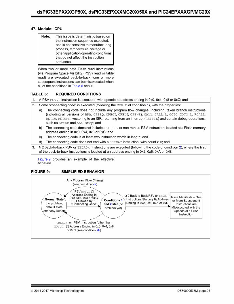
Figure 9 provides an example of the effective behavior.
FIGURE 9: SIMPLIFIED BEHAVIOR
Note: This issue is deterministic based on the instruction sequence executed, and is not sensitive to manufacturing process, temperature, voltage or other application operating conditions that do not affect the instruction sequence.
TABLE 6: REQUIRED CONDITIONS
1. A PSV MOV.D instruction is executed, with opcode at address ending in 0x0, 0x4, 0x8 or 0xC; and
2. Some “connecting code” is executed (following the MOV.D of condition 1), with the properties:
a) The connecting code does not include any program flow changes, including: taken branch instructions (including all versions of BRA, CPBEQ, CPBGT, CPBLT, CPBNE), CALL, CALL.L, GOTO, GOTO.L, RCALL, RETLW, RETURN, vectoring to an ISR, returning from an interrupt (RETFIE) and certain debug operations,such as break and one-step; and
b) The connecting code does not include a TBLRDx or non-MOV.D PSV instruction, located at a Flash memory address ending in 0x0, 0x4, 0x8 or 0xC; and
c) The connecting code is at least two instruction words in length; and
d) The connecting code does not end with a REPEAT instruction, with count > 0; and
3. ≥ 2 back-to-back PSV or TBLRDx instructions are executed (following the code of condition 2), where the first of the back-to-back instructions is located at an address ending in 0x2, 0x6, 0xA or 0xE.
Normal State(no problem, default state
after any Reset)
Conditions 1 and 2 Met (no problem yet)
Issue Manifests – Oneor More Subsequent
Instructions areMisexecuted with the
Opcode of a Prior Instruction
PSV MOV.D @Address Ending in
≥ 2 Back-to-Back PSV or TBLRDxInstructions Starting @ AddressEnding in 0x2, 0x6, 0xA or 0xE
Any Program Flow Change(see condition 2a)
0x0, 0x4, 0x8 or 0xC,
TBLRDx or PSV Instruction (other than MOV.D) @ Address Ending in 0x0, 0x4, 0x8
or 0xC (see condition 2b)
Followed by“Connecting Code”
2011-2017 Microchip Technology Inc. DS80000533M-page 25
dsPIC33EPXXXGP50X, dsPIC33EPXXXMC20X/50X and PIC24EPXXXGP/MC20X
Work around
The issue can be avoided by ensuring any one or more of the requirements are not met. For example:
1. All instances of PSV MOV.D can be replaced with two PSV MOV instructions instead. Non-PSV MOV.D instructions acting on RAM/SFRs do not need to be modified; or
2. If not already present, a program flow change instruction (such as BRA $+2) can be inserted above back-to-back data Flash read sequences; or
3. Back-to-back data Flash read instruction sequences can be broken up by inserting a non-Flash read instruction (such as a NOP) in between the Flash read instructions; or
4. The alignment of the code can be shifted to avoid the required opcode location addresses.
C code built with MPLAB® XC16 Compiler, Version 1.32, or later, implements the work around by default. However, if the application uses Assembly language routines, these should be manually modified to implement the work around. Additionally, if precompiled libraries are used, these should be built with XC16 Version 1.32 or later. For additional information, please visit: www.microchip.com/erratum_psrd_psrd.
Affected Silicon Revisions
dsPIC33/PIC24EP32 devices A3, A8
dsPIC33/PIC24EP64 devices A2, A3, A8
dsPIC33/PIC24EP128 devices A3, A8
dsPIC33/PIC24EP256 devices A3, A8, A9
dsPIC33/PIC24EP512 devices A7
DS80000533M-page 26 2011-2017 Microchip Technology Inc.

dsPIC33EPXXXGP50X, dsPIC33EPXXXMC20X/50X and PIC24EPXXXGP/MC20X
Data Sheet Clarifications
The following typographic corrections and clarifications are to be noted for the latest version of the device data sheet (DS70000657H):
1. Module: Electrical Characteristics
Table 30-53 states incorrect values for some of the parameters. The corrected values are shown in bold below.
Note: Corrections are shown in bold. Where possible, the original bold text formatting has been removed for clarity.
TABLE 30-53: OP AMP/COMPARATOR SPECIFICATIONS
DC CHARACTERISTICS
Standard Operating Conditions: 3.0V to 3.6V(unless otherwise stated)(1)
Operating temperature -40°C TA +85°C for Industrial-40°C TA +125°C for Extended
Param No.
Symbol Characteristic Min. Typ.(2) Max. Units Conditions
Comparator AC Characteristics
CM10 TRESP Response Time(3) — 19 — ns V+ input step of 100 mV,V- input held at VDD/2
CM11 TMC2OV Comparator Mode Change to Output Valid
— — 10 µs
Comparator DC Characteristics
CM30 VOFFSET Comparator Offset Voltage
— ±10 ±15(7) mV
CM31 VHYST Input Hysteresis Voltage(3)
— 30 65(7) mV
CM32 TRISE/TFALL Comparator Output Rise/Fall Time(3)
— 20 — ns 1 pF load capacitance on input
CM34 VICM Input Voltage Range AVSS — AVDD V
Op Amp AC Characteristics
CM20 SR Slew Rate 3.7 7.5 16 V/µs 10 pF load
CM21a PM Phase Margin (Configuration A)(3,4)
— 55 — Degree G = 4V/V; 10 pF load
CM21b PM Phase Margin (Configuration B)(3,5)
— 40 — Degree G = 4V/V; 10 pF load
CM22 GM Gain Margin(3) — 20 — db G = 100V/V; 10 pF load
Note 1: Device is functional at VBORMIN < VDD < VDDMIN, but will have degraded performance. Device functionality is tested, but not characterized. Analog modules (ADC, op amp/comparator and comparator voltage reference) may have degraded performance. Refer to Parameter BO10 in Table 30-13 for the minimum and maximum BOR values.
2: Data in “Typ” column is at 3.3V, +25°C unless otherwise stated.
3: Parameter is characterized but not tested in manufacturing.
4: See Figure 25-6 for configuration information.
5: See Figure 25-7 for configuration information.
6: Resistances can vary by ±10% between op amps.
7: These parameters have a combined effect on the actual performance of the comparator.
2011-2017 Microchip Technology Inc. DS80000533M-page 27
dsPIC33EPXXXGP50X, dsPIC33EPXXXMC20X/50X and PIC24EPXXXGP/MC20X
2. Module: DC and AC Device Characteristics Graphs
The typical LPRC frequency plot over temperature at VDD = 3.3V has been corrected, as shown in Figure 32-10 below.
FIGURE 32-10: TYPICAL LPRC FREQUENCY @ VDD = 3.3V
3. Module: Electrical Characteristics
Table 30-11 had incorrect information in Note 5 and Note 6. The corrected Note 5 and Note 6 are shown below:
5. VIH source > (VDD + 0.3) for non-5V tolerant pins only.
6. Digital 5V tolerant pins do not have an internal high-side diode to VDD, and therefore, cannot tolerate any “positive” input injection current.
4. Module: Electrical Characteristics
Page Erase Time (TPE) Parameters D137a-D137b and Word Write Cycle Time (TWW) Parameters D138a-D138b were incorrectly specified in Table 30-14. The corrected values are shown in bold below.
-40C 25C 125C 150Cmin 25.2 30.8 30 29.6
mean 28.9 32 31.2 30.8max 32.8 34.8 34 33.6
24252627282930313233343536
LPRC Frequency (KHx)
min
mean
max)
LP
RC
Fre
qu
ency
(k
Hz)
TABLE 30-14: DC CHARACTERISTICS: PROGRAM MEMORY
DC CHARACTERISTICS
Standard Operating Conditions: 3.0V to 3.6V(unless otherwise stated)Operating temperature -40°C TA +85°C for Industrial
-40°C TA +125°C for Extended
ParamNo.
Symbol Characteristic Min. Typ.(1) Max. Units Conditions
Program Flash Memory
D130 EP Cell Endurance 10,000 — — E/W -40C to +125C
D131 VPR VDD for Read 3.0 — 3.6 V
D132b VPEW VDD for Self-Timed Write 3.0 — 3.6 V
D134 TRETD Characteristic Retention 20 — — Year Provided no other specifications are violated, -40C to +125C
D135 IDDP Supply Current during Programming(2)
— 10 — mA
D136 IPEAK Instantaneous Peak Current During Start-up
— — 150 mA
D137a TPE Page Erase Time — 146893 — FRCCycles
TA = +85°C
D137b TPE Page Erase Time — 146893 — FRCCycles
TA = +125°C
D138a TWW Word Write Cycle Time — 346 — FRCCycles
TA = +85°C
D138b TWW Word Write Cycle Time — 346 — FRCCycles
TA = +125°C
Note 1: Data in “Typical” column is at 3.3V, +25°C unless otherwise stated.
2: Parameter characterized but not tested in manufacturing.
DS80000533M-page 28 2011-2017 Microchip Technology Inc.

dsPIC33EPXXXGP50X, dsPIC33EPXXXMC20X/50X and PIC24EPXXXGP/MC20X
5. Module: Electrical Characteristics
In Table 30-53, the Feedback Resistance Value parameter (CM48, RFEEDBACK) was missing a note describing the minimum input resistance (R1) requirement and the resulting limitation on the minimum gain. The updated information is shown in bold below.
TABLE 30-53: OP AMP/COMPARATOR SPECIFICATIONS
DC CHARACTERISTICS
Standard Operating Conditions: 3.0V to 3.6V(unless otherwise stated)(1)
Operating temperature -40°C TA +85°C for Industrial-40°C TA +125°C for Extended
Param No.
Symbol Characteristic Min. Typ.(2) Max. Units Conditions
Op Amp DC Characteristics
CM40 VCMR Common-Mode Input Voltage Range
AVSS — AVDD V
CM41 CMRR Common-Mode Rejection Ratio(3)
— 40 — db VCM = AVDD/2
CM42 VOFFSET Op Amp Offset Voltage(3)
— ±5 — mV
CM43 VGAIN Open-Loop Voltage Gain(3)
— 90 — db
CM44 IOS Input Offset Current — — — — See pad leakage currents in Table 30-11
CM45 IB Input Bias Current — — — — See pad leakage currents in Table 30-11
CM46 IOUT Output Current — — 420 µA With minimum value of RFEEDBACK (CM48)
CM48 RFEEDBACK(7) Feedback Resistance Value
8 — — k
CM49a VOADC Output Voltage Measured at OAx Using ADC(3,4)
AVSS + 0.077AVSS + 0.037AVSS + 0.018
———
AVDD – 0.077AVDD – 0.037AVDD – 0.018
VVV
IOUT = 420 µAIOUT = 200 µAIOUT = 100 µA
Note 1: Device is functional at VBORMIN < VDD < VDDMIN, but will have degraded performance. Device functionality is tested, but not characterized. Analog modules (ADC, op amp/comparator and comparator voltage reference) may have degraded performance. Refer to Parameter BO10 in Table 30-13 for the minimum and maximum BOR values.
2: Data in “Typ” column is at 3.3V, +25°C unless otherwise stated.
3: Parameter is characterized but not tested in manufacturing.
4: See Figure 25-6 for configuration information.
5: See Figure 25-7 for configuration information.
6: Resistances can vary by ±10% between op amps.
7: Input resistance (R1) must be less than or equal to 2 kΩ. The resulting minimum gain of the op amp circuit is equal to 4.
2011-2017 Microchip Technology Inc. DS80000533M-page 29

dsPIC33EPXXXGP50X, dsPIC33EPXXXMC20X/50X and PIC24EPXXXGP/MC20X
6. Module: High-Temperature Electrical Characteristics
The High-Temperature Electrical Characteristics section did not include information regarding the FRC accuracy at an operating temperature of +125°C > TA > +150°C. Table 7 provides this missing information.
7. Module: I/O Ports
The first paragraph of Section 11.2 “Configuring Analog and Digital Port Pins” is amended with the following text:
“When ANSEL = 1 (the port is selected as analog) and TRIS = 1 (digital I/O is enabled), the digital input value read by the port is always ‘0’.”
8. Module: 10/12-Bit Analog-to-Digital Converter (ADC)
Note 2 of Register 23-8 (AD1CSSL) is amended with the following text:
“The outputs for Op Amps 1, 2 and 3 can be scanned by selecting analog inputs AN3, AN0 and AN6, respectively.”
9. Module: Comparator/Op Amp
The following text is amended to the end of Section 25.1 “Op Amp Application Considerations”:
“When the op amp output is to be made available on the corresponding OAxOUT pin, set both the pin’s TRISx bit and the corresponding ANSELx bit to ‘1’.”
10. Module: Comparator/Op Amp
Figure 25-1 (shown below) is corrected to show that the op amp in these modules obtains its inverting and non-inverting inputs directly from the CxIN1-/1+ pins. The operation of the actual module is unchanged. (Footnotes in the original are unchanged, but are removed here for clarity.)
FIGURE 25-1: OP AMP/COMPARATOR x MODULE BLOCK DIAGRAM (MODULES 1, 2 AND 3)
TABLE 7: INTERNAL FRC ACCURACY
AC CHARACTERISTICSStandard Operating Conditions: 3.0V to 3.6V (unless otherwise stated)Operating temperature +125°C TA +150°C for High Temperature
ParamNo.
Characteristic Min Typ Max Units Conditions
Internal FRC Accuracy @ FRC Frequency = 7.37 MHz(1)
Hxx FRC -3 -2 +3 % +125°C TA +150°C VDD = 3.0-3.6V
Note 1: Frequency is calibrated at +25°C and 3.3V.
BlankingFunction
DigitalFilter
CxOUT(1)
(see Figure 25-4) (see Figure 25-5) PTG TriggerInput
0
1
00
01
CxIN1+
CVREFIN(1)
CxIN1-
CXIN2-(1)
CMPx
–
+
VIN-
VIN+
CCH<1:0> (CMxCON<1:0>)
CREF (CMxCON<4>)
Op Amp/Comparator(2)
Op Ampx–
+
OAx/ANx(3)
OAxOUT/ANx
OPMODE (CMxCON<10>)
(to ADC)
RINT1
DS80000533M-page 30 2011-2017 Microchip Technology Inc.
dsPIC33EPXXXGP50X, dsPIC33EPXXXMC20X/50X and PIC24EPXXXGP/MC20X
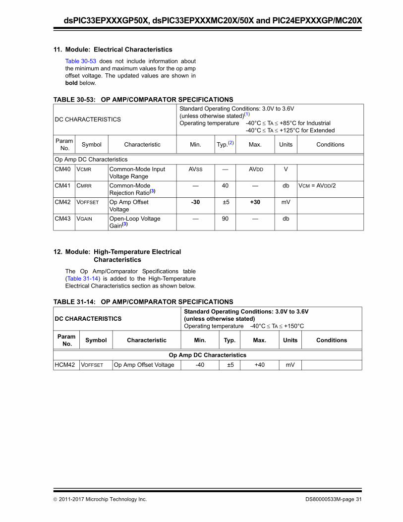
11. Module: Electrical Characteristics
Table 30-53 does not include information about the minimum and maximum values for the op amp offset voltage. The updated values are shown in bold below.
12. Module: High-Temperature Electrical Characteristics
The Op Amp/Comparator Specifications table (Table 31-14) is added to the High-Temperature Electrical Characteristics section as shown below.
TABLE 30-53: OP AMP/COMPARATOR SPECIFICATIONS
DC CHARACTERISTICS
Standard Operating Conditions: 3.0V to 3.6V(unless otherwise stated)(1)
Operating temperature -40°C TA +85°C for Industrial-40°C TA +125°C for Extended
Param No.
Symbol Characteristic Min. Typ.(2) Max. Units Conditions
Op Amp DC Characteristics
CM40 VCMR Common-Mode Input Voltage Range
AVSS — AVDD V
CM41 CMRR Common-Mode Rejection Ratio(3)
— 40 — db VCM = AVDD/2
CM42 VOFFSET Op Amp Offset Voltage
-30 ±5 +30 mV
CM43 VGAIN Open-Loop Voltage Gain(3)
— 90 — db
TABLE 31-14: OP AMP/COMPARATOR SPECIFICATIONS
DC CHARACTERISTICSStandard Operating Conditions: 3.0V to 3.6V(unless otherwise stated)Operating temperature -40°C TA +150°C
Param No.
Symbol Characteristic Min. Typ. Max. Units Conditions
Op Amp DC Characteristics
HCM42 VOFFSET Op Amp Offset Voltage -40 ±5 +40 mV
2011-2017 Microchip Technology Inc. DS80000533M-page 31

dsPIC33EPXXXGP50X, dsPIC33EPXXXMC20X/50X and PIC24EPXXXGP/MC20X
13. Module: Power-Saving Features
In Section 10.0 “Power-Saving Features”, there are two changes included.
Change 1: Example 10-1 is modified to show a condition and a note. The changes are shown below in bold.
EXAMPLE 10-1: PWRSAV INSTRUCTION SYNTAX
Change 2: The fourth paragraph ofSection 10.2.1 “Sleep Mode” is modified to include the condition where the Flash voltage reg-ulator is placed in Standby mode. An additional example is added to show how to implement the SLEEP instruction in a 4-instruction word-aligned function. The modified text is added as follows:
For optimal power savings, the internal regulator and the Flash regulator can be configured to go into standby when Sleep mode is entered by clearing the VREGS (RCON<8>) and VREGSF (RCON<11>) bits (default configuration). However, putting the Flash Voltage Regulator in Standby Mode (VREGSF = 0) when in Sleep has the effect of corrupting the prefetched instructions placed in the instruction queue. When the part wakes up, these instructions may cause undefined behavior. To remove this prob-lem, the instruction queue must be flushed after the part wakes up. A way to flush the instruction queue is to perform a branch. Therefore, it is required to implement the SLEEP instruction in a function with 4-instruction word alignment. The 4-instruction word alignment will assure that the SLEEP instruction is always placed on the correct address to make sure the flushing will be effective. Example 10-2 shows how this is performed.
EXAMPLE 10-2: SLEEP MODE PWRSAV INSTRUCTION SYNTAX (WITH FLASH VOLTAGE REGULATOR SET TO STANDBY MODE)
PWRSAV #IDLE_MODE ; Put the device into Idle modePWRSAV #SLEEP_MODE ; Put the device into Sleep mode(1)
Note 1: The use of PWRSV #SLEEP_MODE has limitations when the Flash Voltage Regulator bit, VREGSF (RCON<11>), is set to Standby mode. Refer to Section 10.2.1 “Sleep Mode” for more information.
.global _GoToSleep
.section .text
.align 4 _GoToSleep: PWRSAV #SLEEP_MODE BRA TO_FLUSH_QUEUE_LABELTO_FLUSH_QUEUE_LABEL:RETURN
DS80000533M-page 32 2011-2017 Microchip Technology Inc.
dsPIC33EPXXXGP50X, dsPIC33EPXXXMC20X/50X and PIC24EPXXXGP/MC20X
APPENDIX A: REVISION HISTORY
Rev A Document (11/2011)
Initial release of this document; issued for revision A2 silicon.
Includes silicon issues 1 (CPU), 2, (CPU) 3 (SPI), 4 (SPI), 5 (UART), 6 (Power System), 7 (ADC), 8 (PTG), 9 (Op Amp), 10 (Op Amp), 11 (PWM), 12 (Flash), 13 (QEI), 14 (QEI) and 15 (PWM).
Rev B Document (4/2012)
Updated silicon issues 9 (Op Amp), 10 (Op Amp), and 12 (Flash).
Added silicon issues 16 (ADC), 17 (ADC), 18 (Output Compare), and 19 (CAN).
Rev C Document (6/2012)
Updated document to include all related device families (program memory sizes of 32, 128, 256 and 512 Kbytes) in this superfamily. In the process, revised the document format to accommodate the different silicon revision levels across the different families.
Added silicon issues 20, 21 and 22 (PWM), and 23 (CPU) to all device families.
Added data sheet clarification 1 (Packaging).
Rev D Document (8/2012)
Updated Table 1 to include both A2 and A3 silicon revision device IDs and removedPIC24EP512/dsPIC32EP512 (A4). Updated all Affected Families and Silicon Revisions tables.
Added silicon issues 24 (PWM) and 25 (PWM).
Added data sheet clarification 2 (High-Speed PWM Module).
Rev E Document (3/2013)
Adds silicon revision A2 for all 64 Kbyte devices to all existing silicon issues, except 9 and 10 (Op Amp).
Revises issue 24 (PWM) with a figure to illustrate the timing of the issue.
Revises issue 25 (PWM) to clarify conditions, and add work around options.
Added new silicon issues 26 (PWM), 27 (CTMU), 28 (Input Capture), 29 (JTAG), 30 (I/O), 31 (JTAG) and 32 (QEI) to silicon revision A3 for all device families, and revision A2 for 64 Kbyte device families only.
Updates data sheet revision level to “G”. Removes previous data sheet clarifications, which have been addressed in the new revision; adds new data sheet clarification 1 (Revision History).
Rev F Document (6/2013)
Updates document to include 512 Kbytes memory. Adds silicon issues 33 (QEI), 34 (QEI), 35 (PWM), 36 (PWM) and 37 (Op Amp/Comparator). Revises silicon issue 15 (PWM) description. Revises silicon issue 20 (PWM)with new figure and text. Revises issue 25 (PWM). Removes data sheet clarification 1 (Pin Diagrams) since this is now addressed in the current data sheet revision.
Rev G Document (9/2013)
Updates document to include revision A8 silicon.
Adds silicon issues 38-40 (PWM).
Modifies the Affected Families and Silicon Revisions table for issue 25 (PWM) with respect to the dsPIC33/PIC24EP512 devices. Updated Figure 1, relevant to issue 20 (PWM).
Rev H Document (02/2014)
Updates document to include silicon revision A8 for 128-Kbyte devices. All references to “ECAN” in this document are now changed to “CAN”.
Added silicon issue 41 (CAN).
Updated Table 2, relevant to issue 41 (CAN). Modifies the Affected Families and Silicon Revisions table for issue 26 (PWM) and issue 36 (PWM).
Rev J Document (3/2014)
Updates document to include silicon revision A8 for 32-Kbyte devices.
Adds data sheet clarifications 1 (Electrical Characteristics), 2 (DC and AC Device Characteristics Graphs), 3 (Electrical Characteristics), 4 (Electrical Characteristics), 5 (Electrical Characteristics) and 6 (High-Temperature Electrical Characteristics).
Rev K Document (7/2014)
Updates document to add silicon revision A8 to all 256 Kbyte devices. Adds all existing silicon issues affecting silicon revision A8 for 64 Kbyte devices to revision A8 for 256 Kbyte devices.
Adds new silicon issues 42, 43 and 44 (PWM).
Amends silicon issue 4 (SPI) by correcting the state of the SPIFSD bit to ‘0’. (The text of the issue is otherwise unaffected and the issue is unchanged.)
Amends silicon issue 8 (PTG) by correcting the base prefix of the affected commands to ‘0b’ instead of ‘0h’. (The text of the issue is otherwise unaffected and the issue is unchanged.)
Amends Table 5 in the work around for silicon issue 36 (PWM) by deleting the row corresponding to PCLKDIV<2:0> = 111, since this is a reserved setting. The basic issue is unchanged.
Amends silicon issue 38 (PWM) by adding additional text to the first paragraph to clarify the nature of the observed glitch. The basic issue is unchanged.
Adds data sheet clarifications 7 (I/O Ports), 8 (10/12-Bit Analog-to-Digital Converter (ADC)) and 9-10 (Comparator/Op Amp).
Rev L Document (12/2014)
Adds silicon revision A9 to dsPIC33EP256MC506. Adds silicon issues 45 (PWM) and 46 (PWM). Adds data sheet clarification 11 (Electrical Characteristics), 12 (High-Temperature Electrical Characteristics) and 13 (Power-Saving Features).
Rev M Document (8/2017)
Updates silicon issue 2 (CPU).
Adds silicon issue 47 (CPU).
2011-2017 Microchip Technology Inc. DS80000533M-page 33

dsPIC33EPXXXGP50X, dsPIC33EPXXXMC20X/50X and PIC24EPXXXGP/MC20X
NOTES:
DS80000533M-page 34 2011-2017 Microchip Technology Inc.

Note the following details of the code protection feature on Microchip devices:
• Microchip products meet the specification contained in their particular Microchip Data Sheet.
• Microchip believes that its family of products is one of the most secure families of its kind on the market today, when used in the intended manner and under normal conditions.
• There are dishonest and possibly illegal methods used to breach the code protection feature. All of these methods, to our knowledge, require using the Microchip products in a manner outside the operating specifications contained in Microchip’s Data Sheets. Most likely, the person doing so is engaged in theft of intellectual property.
• Microchip is willing to work with the customer who is concerned about the integrity of their code.
• Neither Microchip nor any other semiconductor manufacturer can guarantee the security of their code. Code protection does not mean that we are guaranteeing the product as “unbreakable.”
Code protection is constantly evolving. We at Microchip are committed to continuously improving the code protection features of ourproducts. Attempts to break Microchip’s code protection feature may be a violation of the Digital Millennium Copyright Act. If such actsallow unauthorized access to your software or other copyrighted work, you may have a right to sue for relief under that Act.
Information contained in this publication regarding deviceapplications and the like is provided only for your convenienceand may be superseded by updates. It is your responsibility toensure that your application meets with your specifications.MICROCHIP MAKES NO REPRESENTATIONS ORWARRANTIES OF ANY KIND WHETHER EXPRESS ORIMPLIED, WRITTEN OR ORAL, STATUTORY OROTHERWISE, RELATED TO THE INFORMATION,INCLUDING BUT NOT LIMITED TO ITS CONDITION,QUALITY, PERFORMANCE, MERCHANTABILITY ORFITNESS FOR PURPOSE. Microchip disclaims all liabilityarising from this information and its use. Use of Microchipdevices in life support and/or safety applications is entirely atthe buyer’s risk, and the buyer agrees to defend, indemnify andhold harmless Microchip from any and all damages, claims,suits, or expenses resulting from such use. No licenses areconveyed, implicitly or otherwise, under any Microchipintellectual property rights unless otherwise stated.
2011-2017 Microchip Technology Inc.
Microchip received ISO/TS-16949:2009 certification for its worldwide headquarters, design and wafer fabrication facilities in Chandler and Tempe, Arizona; Gresham, Oregon and design centers in California and India. The Company’s quality system processes and procedures are for its PIC® MCUs and dsPIC® DSCs, KEELOQ® code hopping devices, Serial EEPROMs, microperipherals, nonvolatile memory and analog products. In addition, Microchip’s quality system for the design and manufacture of development systems is ISO 9001:2000 certified.
QUALITY MANAGEMENT SYSTEM CERTIFIED BY DNV
== ISO/TS 16949 ==
Trademarks
The Microchip name and logo, the Microchip logo, AnyRate, AVR, AVR logo, AVR Freaks, BeaconThings, BitCloud, CryptoMemory, CryptoRF, dsPIC, FlashFlex, flexPWR, Heldo, JukeBlox, KEELOQ, KEELOQ logo, Kleer, LANCheck, LINK MD, maXStylus, maXTouch, MediaLB, megaAVR, MOST, MOST logo, MPLAB, OptoLyzer, PIC, picoPower, PICSTART, PIC32 logo, Prochip Designer, QTouch, RightTouch, SAM-BA, SpyNIC, SST, SST Logo, SuperFlash, tinyAVR, UNI/O, and XMEGA are registered trademarks of Microchip Technology Incorporated in the U.S.A. and other countries.
ClockWorks, The Embedded Control Solutions Company, EtherSynch, Hyper Speed Control, HyperLight Load, IntelliMOS, mTouch, Precision Edge, and Quiet-Wire are registered trademarks of Microchip Technology Incorporated in the U.S.A.
Adjacent Key Suppression, AKS, Analog-for-the-Digital Age, Any Capacitor, AnyIn, AnyOut, BodyCom, chipKIT, chipKIT logo, CodeGuard, CryptoAuthentication, CryptoCompanion, CryptoController, dsPICDEM, dsPICDEM.net, Dynamic Average Matching, DAM, ECAN, EtherGREEN, In-Circuit Serial Programming, ICSP, Inter-Chip Connectivity, JitterBlocker, KleerNet, KleerNet logo, Mindi, MiWi, motorBench, MPASM, MPF, MPLAB Certified logo, MPLIB, MPLINK, MultiTRAK, NetDetach, Omniscient Code Generation, PICDEM, PICDEM.net, PICkit, PICtail, PureSilicon, QMatrix, RightTouch logo, REAL ICE, Ripple Blocker, SAM-ICE, Serial Quad I/O, SMART-I.S., SQI, SuperSwitcher, SuperSwitcher II, Total Endurance, TSHARC, USBCheck, VariSense, ViewSpan, WiperLock, Wireless DNA, and ZENA are trademarks of Microchip Technology Incorporated in the U.S.A. and other countries.
SQTP is a service mark of Microchip Technology Incorporated in the U.S.A.
Silicon Storage Technology is a registered trademark of Microchip Technology Inc. in other countries.
GestIC is a registered trademark of Microchip Technology Germany II GmbH & Co. KG, a subsidiary of Microchip Technology Inc., in other countries.
All other trademarks mentioned herein are property of their respective companies.
© 2011-2017, Microchip Technology Incorporated, All Rights Reserved.
ISBN: 978-1-5224-2095-8
DS80000533M-page 35

DS80000533M-page 36 2011-2017 Microchip Technology Inc.
AMERICASCorporate Office2355 West Chandler Blvd.Chandler, AZ 85224-6199Tel: 480-792-7200 Fax: 480-792-7277Technical Support: http://www.microchip.com/supportWeb Address: www.microchip.com
AtlantaDuluth, GA Tel: 678-957-9614 Fax: 678-957-1455
Austin, TXTel: 512-257-3370
BostonWestborough, MA Tel: 774-760-0087 Fax: 774-760-0088
ChicagoItasca, IL Tel: 630-285-0071 Fax: 630-285-0075
DallasAddison, TX Tel: 972-818-7423 Fax: 972-818-2924
DetroitNovi, MI Tel: 248-848-4000
Houston, TX Tel: 281-894-5983
IndianapolisNoblesville, IN Tel: 317-773-8323Fax: 317-773-5453Tel: 317-536-2380
Los AngelesMission Viejo, CA Tel: 949-462-9523Fax: 949-462-9608Tel: 951-273-7800
Raleigh, NC Tel: 919-844-7510
New York, NY Tel: 631-435-6000
San Jose, CA Tel: 408-735-9110Tel: 408-436-4270
Canada - TorontoTel: 905-695-1980 Fax: 905-695-2078
ASIA/PACIFICAsia Pacific OfficeSuites 3707-14, 37th FloorTower 6, The GatewayHarbour City, Kowloon
Hong KongTel: 852-2943-5100Fax: 852-2401-3431
Australia - SydneyTel: 61-2-9868-6733Fax: 61-2-9868-6755
China - BeijingTel: 86-10-8569-7000 Fax: 86-10-8528-2104
China - ChengduTel: 86-28-8665-5511Fax: 86-28-8665-7889
China - ChongqingTel: 86-23-8980-9588Fax: 86-23-8980-9500
China - DongguanTel: 86-769-8702-9880
China - GuangzhouTel: 86-20-8755-8029
China - HangzhouTel: 86-571-8792-8115 Fax: 86-571-8792-8116
China - Hong Kong SARTel: 852-2943-5100 Fax: 852-2401-3431
China - NanjingTel: 86-25-8473-2460Fax: 86-25-8473-2470
China - QingdaoTel: 86-532-8502-7355Fax: 86-532-8502-7205
China - ShanghaiTel: 86-21-3326-8000 Fax: 86-21-3326-8021
China - ShenyangTel: 86-24-2334-2829Fax: 86-24-2334-2393
China - ShenzhenTel: 86-755-8864-2200 Fax: 86-755-8203-1760
China - WuhanTel: 86-27-5980-5300Fax: 86-27-5980-5118
China - XianTel: 86-29-8833-7252Fax: 86-29-8833-7256
ASIA/PACIFICChina - XiamenTel: 86-592-2388138 Fax: 86-592-2388130
China - ZhuhaiTel: 86-756-3210040 Fax: 86-756-3210049
India - BangaloreTel: 91-80-3090-4444 Fax: 91-80-3090-4123
India - New DelhiTel: 91-11-4160-8631Fax: 91-11-4160-8632
India - PuneTel: 91-20-3019-1500
Japan - OsakaTel: 81-6-6152-7160 Fax: 81-6-6152-9310
Japan - TokyoTel: 81-3-6880- 3770 Fax: 81-3-6880-3771
Korea - DaeguTel: 82-53-744-4301Fax: 82-53-744-4302
Korea - SeoulTel: 82-2-554-7200Fax: 82-2-558-5932 or 82-2-558-5934
Malaysia - Kuala LumpurTel: 60-3-6201-9857Fax: 60-3-6201-9859
Malaysia - PenangTel: 60-4-227-8870Fax: 60-4-227-4068
Philippines - ManilaTel: 63-2-634-9065Fax: 63-2-634-9069
SingaporeTel: 65-6334-8870Fax: 65-6334-8850
Taiwan - Hsin ChuTel: 886-3-5778-366Fax: 886-3-5770-955
Taiwan - KaohsiungTel: 886-7-213-7830
Taiwan - TaipeiTel: 886-2-2508-8600 Fax: 886-2-2508-0102
Thailand - BangkokTel: 66-2-694-1351Fax: 66-2-694-1350
EUROPEAustria - WelsTel: 43-7242-2244-39Fax: 43-7242-2244-393
Denmark - CopenhagenTel: 45-4450-2828 Fax: 45-4485-2829
Finland - EspooTel: 358-9-4520-820
France - ParisTel: 33-1-69-53-63-20 Fax: 33-1-69-30-90-79
France - Saint CloudTel: 33-1-30-60-70-00
Germany - GarchingTel: 49-8931-9700Germany - HaanTel: 49-2129-3766400
Germany - HeilbronnTel: 49-7131-67-3636
Germany - KarlsruheTel: 49-721-625370
Germany - MunichTel: 49-89-627-144-0 Fax: 49-89-627-144-44
Germany - RosenheimTel: 49-8031-354-560
Israel - Ra’anana Tel: 972-9-744-7705
Italy - Milan Tel: 39-0331-742611 Fax: 39-0331-466781
Italy - PadovaTel: 39-049-7625286
Netherlands - DrunenTel: 31-416-690399 Fax: 31-416-690340
Norway - TrondheimTel: 47-7289-7561
Poland - WarsawTel: 48-22-3325737
Romania - BucharestTel: 40-21-407-87-50
Spain - MadridTel: 34-91-708-08-90Fax: 34-91-708-08-91
Sweden - GothenbergTel: 46-31-704-60-40
Sweden - StockholmTel: 46-8-5090-4654
UK - WokinghamTel: 44-118-921-5800Fax: 44-118-921-5820
Worldwide Sales and Service
11/07/16